EP4152611B1 - Kristalloszillator und verfahren zu seiner herstellung - Google Patents
Kristalloszillator und verfahren zu seiner herstellung Download PDFInfo
- Publication number
- EP4152611B1 EP4152611B1 EP22191660.4A EP22191660A EP4152611B1 EP 4152611 B1 EP4152611 B1 EP 4152611B1 EP 22191660 A EP22191660 A EP 22191660A EP 4152611 B1 EP4152611 B1 EP 4152611B1
- Authority
- EP
- European Patent Office
- Prior art keywords
- electrode portion
- extending
- substrate
- support frame
- electrode
- Prior art date
- Legal status (The legal status is an assumption and is not a legal conclusion. Google has not performed a legal analysis and makes no representation as to the accuracy of the status listed.)
- Active
Links
Images



Classifications
-
- H—ELECTRICITY
- H03—ELECTRONIC CIRCUITRY
- H03H—IMPEDANCE NETWORKS, e.g. RESONANT CIRCUITS; RESONATORS
- H03H9/00—Networks comprising electromechanical or electro-acoustic elements; Electromechanical resonators
- H03H9/15—Constructional features of resonators consisting of piezoelectric or electrostrictive material
- H03H9/17—Constructional features of resonators consisting of piezoelectric or electrostrictive material having a single resonator
- H03H9/19—Constructional features of resonators consisting of piezoelectric or electrostrictive material having a single resonator consisting of quartz
-
- H—ELECTRICITY
- H03—ELECTRONIC CIRCUITRY
- H03H—IMPEDANCE NETWORKS, e.g. RESONANT CIRCUITS; RESONATORS
- H03H3/00—Apparatus or processes specially adapted for the manufacture of impedance networks, resonating circuits, resonators
- H03H3/007—Apparatus or processes specially adapted for the manufacture of impedance networks, resonating circuits, resonators for the manufacture of electromechanical resonators or networks
- H03H3/02—Apparatus or processes specially adapted for the manufacture of impedance networks, resonating circuits, resonators for the manufacture of electromechanical resonators or networks for the manufacture of piezoelectric or electrostrictive resonators or networks
-
- H—ELECTRICITY
- H03—ELECTRONIC CIRCUITRY
- H03B—GENERATION OF OSCILLATIONS, DIRECTLY OR BY FREQUENCY-CHANGING, BY CIRCUITS EMPLOYING ACTIVE ELEMENTS WHICH OPERATE IN A NON-SWITCHING MANNER; GENERATION OF NOISE BY SUCH CIRCUITS
- H03B5/00—Generation of oscillations using amplifier with regenerative feedback from output to input
- H03B5/30—Generation of oscillations using amplifier with regenerative feedback from output to input with frequency-determining element being electromechanical resonator
- H03B5/32—Generation of oscillations using amplifier with regenerative feedback from output to input with frequency-determining element being electromechanical resonator being a piezoelectric resonator
- H03B5/36—Generation of oscillations using amplifier with regenerative feedback from output to input with frequency-determining element being electromechanical resonator being a piezoelectric resonator active element in amplifier being semiconductor device
- H03B5/366—Generation of oscillations using amplifier with regenerative feedback from output to input with frequency-determining element being electromechanical resonator being a piezoelectric resonator active element in amplifier being semiconductor device and comprising means for varying the frequency by a variable voltage or current
-
- H—ELECTRICITY
- H03—ELECTRONIC CIRCUITRY
- H03H—IMPEDANCE NETWORKS, e.g. RESONANT CIRCUITS; RESONATORS
- H03H9/00—Networks comprising electromechanical or electro-acoustic elements; Electromechanical resonators
- H03H9/02—Details
- H03H9/02007—Details of bulk acoustic wave devices
- H03H9/02015—Characteristics of piezoelectric layers, e.g. cutting angles
- H03H9/02023—Characteristics of piezoelectric layers, e.g. cutting angles consisting of quartz
-
- H—ELECTRICITY
- H03—ELECTRONIC CIRCUITRY
- H03H—IMPEDANCE NETWORKS, e.g. RESONANT CIRCUITS; RESONATORS
- H03H9/00—Networks comprising electromechanical or electro-acoustic elements; Electromechanical resonators
- H03H9/02—Details
- H03H9/02007—Details of bulk acoustic wave devices
- H03H9/02086—Means for compensation or elimination of undesirable effects
- H03H9/02125—Means for compensation or elimination of undesirable effects of parasitic elements
-
- H—ELECTRICITY
- H03—ELECTRONIC CIRCUITRY
- H03H—IMPEDANCE NETWORKS, e.g. RESONANT CIRCUITS; RESONATORS
- H03H9/00—Networks comprising electromechanical or electro-acoustic elements; Electromechanical resonators
- H03H9/02—Details
- H03H9/05—Holders or supports
- H03H9/0538—Constructional combinations of supports or holders with electromechanical or other electronic elements
- H03H9/0547—Constructional combinations of supports or holders with electromechanical or other electronic elements consisting of a vertical arrangement
- H03H9/0561—Constructional combinations of supports or holders with electromechanical or other electronic elements consisting of a vertical arrangement consisting of a multilayered structure
-
- H—ELECTRICITY
- H10—SEMICONDUCTOR DEVICES; ELECTRIC SOLID-STATE DEVICES NOT OTHERWISE PROVIDED FOR
- H10N—ELECTRIC SOLID-STATE DEVICES NOT OTHERWISE PROVIDED FOR
- H10N30/00—Piezoelectric or electrostrictive devices
- H10N30/80—Constructional details
- H10N30/85—Piezoelectric or electrostrictive active materials
-
- H—ELECTRICITY
- H10—SEMICONDUCTOR DEVICES; ELECTRIC SOLID-STATE DEVICES NOT OTHERWISE PROVIDED FOR
- H10N—ELECTRIC SOLID-STATE DEVICES NOT OTHERWISE PROVIDED FOR
- H10N30/00—Piezoelectric or electrostrictive devices
- H10N30/80—Constructional details
- H10N30/87—Electrodes or interconnections, e.g. leads or terminals
-
- H—ELECTRICITY
- H03—ELECTRONIC CIRCUITRY
- H03H—IMPEDANCE NETWORKS, e.g. RESONANT CIRCUITS; RESONATORS
- H03H3/00—Apparatus or processes specially adapted for the manufacture of impedance networks, resonating circuits, resonators
- H03H3/007—Apparatus or processes specially adapted for the manufacture of impedance networks, resonating circuits, resonators for the manufacture of electromechanical resonators or networks
- H03H3/02—Apparatus or processes specially adapted for the manufacture of impedance networks, resonating circuits, resonators for the manufacture of electromechanical resonators or networks for the manufacture of piezoelectric or electrostrictive resonators or networks
- H03H2003/023—Apparatus or processes specially adapted for the manufacture of impedance networks, resonating circuits, resonators for the manufacture of electromechanical resonators or networks for the manufacture of piezoelectric or electrostrictive resonators or networks the resonators or networks being of the membrane type
-
- H—ELECTRICITY
- H03—ELECTRONIC CIRCUITRY
- H03H—IMPEDANCE NETWORKS, e.g. RESONANT CIRCUITS; RESONATORS
- H03H3/00—Apparatus or processes specially adapted for the manufacture of impedance networks, resonating circuits, resonators
- H03H3/007—Apparatus or processes specially adapted for the manufacture of impedance networks, resonating circuits, resonators for the manufacture of electromechanical resonators or networks
- H03H3/02—Apparatus or processes specially adapted for the manufacture of impedance networks, resonating circuits, resonators for the manufacture of electromechanical resonators or networks for the manufacture of piezoelectric or electrostrictive resonators or networks
- H03H3/04—Apparatus or processes specially adapted for the manufacture of impedance networks, resonating circuits, resonators for the manufacture of electromechanical resonators or networks for the manufacture of piezoelectric or electrostrictive resonators or networks for obtaining desired frequency or temperature coefficient
- H03H2003/0414—Resonance frequency
- H03H2003/0421—Modification of the thickness of an element
- H03H2003/0435—Modification of the thickness of an element of a piezoelectric layer
-
- H—ELECTRICITY
- H03—ELECTRONIC CIRCUITRY
- H03H—IMPEDANCE NETWORKS, e.g. RESONANT CIRCUITS; RESONATORS
- H03H9/00—Networks comprising electromechanical or electro-acoustic elements; Electromechanical resonators
- H03H9/02—Details
- H03H9/05—Holders or supports
- H03H9/10—Mounting in enclosures
- H03H9/1007—Mounting in enclosures for bulk acoustic wave [BAW] devices
- H03H9/1014—Mounting in enclosures for bulk acoustic wave [BAW] devices the enclosure being defined by a frame built on a substrate and a cap, the frame having no mechanical contact with the BAW device
-
- H—ELECTRICITY
- H03—ELECTRONIC CIRCUITRY
- H03H—IMPEDANCE NETWORKS, e.g. RESONANT CIRCUITS; RESONATORS
- H03H9/00—Networks comprising electromechanical or electro-acoustic elements; Electromechanical resonators
- H03H9/02—Details
- H03H9/05—Holders or supports
- H03H9/10—Mounting in enclosures
- H03H9/1007—Mounting in enclosures for bulk acoustic wave [BAW] devices
- H03H9/1035—Mounting in enclosures for bulk acoustic wave [BAW] devices the enclosure being defined by two sealing substrates sandwiching the piezoelectric layer of the BAW device
Definitions
- the disclosure relates to an oscillator and a method for making the same, and more particularly to a crystal oscillator having a high oscillation frequency, and a method for making the same.
- a quartz crystal is a ceramic piezoelectric material, and is often used to make crystal oscillators with high oscillation frequencies, so that the quartz crystal is capable of being applied to various electronic products.
- the conventional crystal oscillator generally includes an oscillation plate made of quartz crystal, and two electrodes that are respectively formed on two opposite surfaces of the oscillation plate and that are used for external electrical connection.
- the oscillation plate is partially thinned, and after that, a thick frame that is made of a material that is the same as that of the oscillation plate, is formed and surrounds the thinned oscillation plate to increase the mechanical support of the thinned oscillation plate.
- a frame can be used as a pick-up portion, or can act as a connection region to connect to other electronic devices.
- Japanese Invention Patent Application Publication No. JP2014154994A discloses an oscillation device in which a substrate of the oscillation device includes a flat oscillation portion, and a thick portion (e.g., a frame) that is integrally formed with the flat oscillation portion and that is used to increase the support of the oscillation device. By controlling the overall thickness of the substrate of the oscillation device, a predetermined oscillation frequency of the oscillation device can be attained.
- the crystal oscillator includes a thick frame
- electrodes of the crystal oscillator are formed across the frame during the manufacturing process, resulting in a poor yield of the electrodes and adversely affecting the production quality of the crystal oscillator.
- JP2015080007A discloses a crystal oscillator comprising an electrode portion on a side surface of the oscillating portion extending to outside of a support frame.
- An object of the disclosure is to provide a crystal oscillator, and a method for making the same, which can alleviate or overcome the aforesaid shortcomings of the prior art.
- a method for making a crystal oscillator includes the steps of:
- a crystal oscillator includes an oscillating substrate, a first electrode, a second electrode, and a support frame.
- the oscillating substrate has a first surface, a second surface opposite to the first surface, and a side surface interconnecting the first surface and the second surface.
- the first electrode includes a first electrode portion disposed on the first surface of the oscillating substrate, and a first extending electrode portion extending from the first electrode portion on the first surface along the side surface to the second surface.
- the second electrode is disposed on the second surface of the oscillating substrate, and includes a second electrode portion and a second extending electrode portion extending from the second electrode portion toward the first extending electrode portion on the second surface.
- a projection of the second electrode portion on the second surface of the oscillating substrate partially overlaps a projection of the first electrode portion on the second surface of the oscillating substrate.
- the second extending electrode portion and the first extending electrode portion are located at a same side of the oscillating substrate.
- the support frame is made of a photoresist material, and is disposed on the second surface of the oscillating substrate.
- the support frame 5 surrounds the second electrode portion. At least a portion of the second extending electrode portion is located outside the support frame.
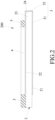
- an embodiment of a crystal oscillator 200 includes an oscillating substrate 2, a first electrode 3, a second electrode 4, and a support frame 5.
- the oscillating substrate 2 has a first surface 21, a second surface 22 opposite to the first surface 21, and a side surface 24 interconnecting the first surface 21 and the second surface 22.
- the oscillating substrate 2 is made of quartz crystal, and has a thickness that is not greater than 50 um. In certain embodiments, the thickness of the oscillating substrate 2 is not greater than 10 um.
- the first electrode 3 includes a first electrode portion 31 disposed on the first surface 21 of the oscillating substrate 2, and a first extending electrode portion 32 extending from the first electrode portion 31 on the first surface 21 along the side surface 24 to the second surface 22.
- the second electrode 4 is disposed on the second surface 22 of the oscillating substrate 2, and includes a second electrode portion 41 and a second extending electrode portion 42 extending from the second electrode portion 41 toward the first extending electrode portion 32 (not shown) on the second surface 22.
- a projection of the second electrode portion 41 on the second surface 22 of the oscillating substrate 2 partially overlaps a projection of the first electrode portion 31 on the second surface 22 of the oscillating substrate 2.
- the second extending electrode portion 42 and the first extending electrode portion 32 are spaced apart from each other and are located at a same side of the oscillating substrate 2.
- Each of the first electrode 3 and the second electrode 4 is independently made from gold, silver, aluminum, or combinations thereof.
- the first electrode 3 and the second electrode 4 may be made of the same or different materials.
- the support frame 5 is made of a photoresist material, and is disposed on the second surface 22 of the oscillating substrate 2.
- the photoresist material may be one of a positive photoresist and a negative photoresist.
- the support frame 5 may have a thickness ranging from 10 um to 100 um.
- the support frame 5 surrounds the second electrode portion 41, and at least a portion of the second extending electrode portion 42 is located outside the support frame 5.
- the second surface 22 of the oscillating substrate 2 includes at least one peripheral area 23 that is located outside and exposed from the support frame 5 (see FIG. 2 ).
- the first extending electrode portion 32 and the second extending electrode portion 42 are located on the at least one peripheral area 23.
- the second extending electrode portion 42 extends from the second electrode portion 41, passes through a region defined between the support frame 5 and the oscillating substrate 2 and terminates at the at least one peripheral area 23, and the first extending electrode portion 32 extends from the first electrode portion 31 on the first surface 21 onto the at least one peripheral area 23.
- the first extending electrode portion 32 and the second extending electrode portion 42 are formed on the second surface 22, which is conducive for external electrical connection, and which facilitates the disposing of the crystal oscillator 200 in electronic products in subsequent applications.
- the support frame 5 is formed as a ring structure.
- the support frame 5 may include at least two strip structures which are located at two sides (e.g., two opposite sides) of the oscillating substrate 2.
- the support frame 5 may be formed as an interrupted ring structure.
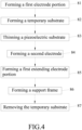
- this disclosure also provides a method for making the embodiment of the crystal oscillator 200, which includes the following steps S81 to S88.
- the first electrode portion 31 is formed on a surface of a piezoelectric substrate 20 made of quartz, so as to obtain a semi-finished product 300.
- the first electrode portion 31 is formed by depositing or printing a conductive material on the surface of the piezoelectric substrate 20.
- step S82 the semi-finished product 300 is attached to a temporary substrate 6 with the first electrode portion 31 facing the temporary substrate 6.
- the temporary substrate 6 may be made of glass, acrylic or ceramic, and is used to support the piezoelectric substrate 20, so as to prevent the piezoelectric substrate 20 from breaking due to poor mechanical strength in the subsequent process (e.g., step S83) .
- step S83 the piezoelectric substrate 20 of the semi-finished product 300 is thinned by a polishing process or chemical etching process, so as to obtain the oscillating substrate 2 having the first surface 21 on which the first electrode portion 31 is formed.
- the thickness of the oscillating substrate 2 may vary depending on the desired oscillation frequency, and the oscillating substrate 2 may have a uniform thickness. In certain embodiments, the thickness of the oscillating substrate 2 is not larger than 50 um. In certain embodiments, when the crystal oscillator 200 is a high frequency oscillator, the thickness of the oscillating substrate 2 may not be larger than 10 um.
- the second electrode 4 is formed on the second surface 22 of the oscillating substrate 2.
- the second electrode 4 includes the second electrode portion 41 in positional correspondence with the first electrode portion 31, and the second extending electrode portion 42 (see FIGS. 1 and 3 ) extending outwardly from the second electrode portion 41 and disposed on a periphery area of the oscillating substrate 2.
- the second electrode 4 is formed by depositing or printing a conductive material on the second surface 22 of the oscillating substrate 2.
- the first extending electrode portion 32 extends from the first electrode portion 31 along the side surface 24 of the oscillating substrate 2 to the second surface 22 of the oscillating substrate 2.
- the first electrode portion 31 and the first extending electrode portion 32 cooperates to form the first electrode 3.
- the first extending electrode portion 32 is formed by printing or depositing a conductive material on the side surface 24 and the second surface 22 of the oscillating substrate 2.
- the first extending electrode portion 32 and the second extending electrode portion 42 are disposed on the second surface 22 of the oscillating substrate 2.
- step S85 may be conducted by forming a portion of the first extending electrode portion 32 on the second surface 22 of the oscillating substrate 2, followed by forming a conductive material (e.g., a silver paste) on the side surface 24 to interconnect the first electrode portion 31 and the portion of the first extending electrode portion 32 on the second surface 22 of the oscillating substrate 2.
- a conductive material e.g., a silver paste
- the conductive material and the portion of the first extending electrode portion 32 constitute the first extending electrode portion 32.
- step S85 may be conducted after step S83 and before step S84.
- step S86 the support frame 5 is formed on the second surface 22 of the oscillating substrate 2.
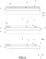
- Step S86 may include (i) coating a photoresist layer 7 (e.g., a positive photoresist or a negative photoresist) having a predetermined thickness on the second surface 22 (see FIG. 6 ), and then (ii) removing a portion of the photoresist layer 7 by photolithography process, so as to form the support frame 5 into a predetermined shape on the second surface 22 of the oscillating substrate 2.
- a photoresist layer 7 e.g., a positive photoresist or a negative photoresist
- the thickness, width, shape, and location of the support frame 5 can be precisely controlled to meet the design requirements.
- the details and parameters of the coating and photolithography processes e.g., the thickness of the photoresist layer 7, exposure wavelength, exposure intensity, or exposure time
- a method for forming the patterned mask may vary depending on the material for the photoresist layer 7).
- the coating and photolithography processes are known to those skilled in the art, and therefore are omitted for the sake of brevity.
- step S87 the temporary substrate 6 is removed from the first electrode portion 31 on the first surface 21 of the oscillating substrate 2.
- Procedure for implementing step S87 may be chosen according to the procedure for attaching the temporary substrate 6 on the first electrode portion 31 in step S82.
- step S87 may be conducted using light radiation or heat application so as to decompose the photosensitive adhesive or the thermo-sensitive adhesive, thereby removing the temporary substrate 6 from the first electrode portion 31.
- the thickness, width, shape, and location of the support frame 5 can be precisely controlled through adjusting the parameters of the coating process and the patterned mask of the photolithography process, so that the thickness of the crystal oscillator 200 (i.e., the thickness of the oscillating substrate 2 and the thickness of the support frame 5) can be further controlled, which enables the crystal oscillator 200 to have the expected oscillation frequency.
Landscapes
- Physics & Mathematics (AREA)
- Acoustics & Sound (AREA)
- Engineering & Computer Science (AREA)
- Manufacturing & Machinery (AREA)
- Piezo-Electric Or Mechanical Vibrators, Or Delay Or Filter Circuits (AREA)
Claims (12)
- Verfahren zur Herstellung eines Kristalloszillators (200), das die folgenden Schritte aufweist:a) Bilden eines ersten Elektrodenteils (31) auf einer Oberfläche eines piezoelektrischen Substrats (20), um ein Halbzeug (300) zu erhalten;b) Ausdünnen des piezoelektrischen Substrats (20) des Halbzeugs (300), um ein schwingendes Substrat (2) zu erhalten, wobei das schwingende Substrat eine erste Oberfläche (21) aufweist, auf der das erste Elektrodenteil (31) gebildet ist;c) Bilden einer zweiten Elektrode (4) auf einer zweiten Oberfläche (22) des schwingenden Substrats (2), die der ersten Oberfläche (21) entgegengesetzt ist, wobei die zweite Elektrode (4) einen zweiten Elektrodenteil (41) in positioneller Übereinstimmung mit dem ersten Elektrodenteil (31) und einen zweiten sich erstreckenden Elektrodenteil (42), der sich auswärts des zweiten Elektrodenteils (41) erstreckt und an einem Randbereich des schwingenden Substrats (2) angeordnet ist, beinhaltet;d) Bilden eines ersten sich erstreckenden Elektrodenteils (32), der sich von dem ersten Elektrodenteil (31) an einer Seitenfläche (24) des schwingenden Substrats (2) entlang zur zweiten Oberfläche (22) des schwingenden Substrats (2) erstreckt, wobei der erste Elektrodenteil (31) und der erste sich erstreckende Elektrodenteil (32) zusammenwirkend eine erste Elektrode bilden; gekennzeichnet durche) Bilden eines tragenden Rahmens (5) auf der zweiten Oberfläche (22) des schwingenden Substrats (2), wobei der tragende Rahmen (5) aus einem Fotolackmaterial hergestellt ist und den zweiten Elektrodenteil (41) umgibt, wobei wenigstens ein Teil des zweiten sich erstreckenden Elektrodenteils (42) außerhalb des tragenden Rahmens (5) liegt.
- Verfahren nach Anspruch 1, ferner gekennzeichnet durch, nach Schritt a) und vor Schritt b), Anbringen des Halbzeugs (300) auf einem provisorischen Substrat (6), wobei der erste Elektrodenteil (31) dem provisorischen Substrat (6) gegenüberliegt.
- Verfahren nach Anspruch 2, das ferner gekennzeichnet ist durch, nach Schritt e), Entfernen des provisorischen Substrats (6) von dem ersten Elektrodenteil (31) auf der ersten Oberfläche (21) des schwingenden Substrats (2).
- Verfahren nach einem der Ansprüche 1 bis 3, dadurch gekennzeichnet, dass das Fotolackmaterial einer von einem Positivfotolack und einem Negativfotolack ist.
- Verfahren nach einem der Ansprüche 1 bis 4, dadurch gekennzeichnet, dass der erste Elektrodenteil (31) und die zweite Elektrode (4) jeweils aus einem leitfähigen Material hergestellt werden und die Schritte a) und c) von einem von dem Aufbringungsprozess und dem Druckprozess durchgeführt werden.
- Verfahren nach einem der Ansprüche 1 bis 5, dadurch gekennzeichnet, dass der erste sich erstreckende Elektrodenteil (32) aus einem leitfähigen Material hergestellt ist und Schritt d) von einem von dem Druckprozess und dem Aufbringungsprozess durchgeführt wird.
- Verfahren nach einem der Ansprüche 1 bis 6, dadurch gekennzeichnet, dass der erste Elektrodenteil (31), der erste sich erstreckende Elektrodenteil (32) und die zweite Elektrode (4) jeweils unabhängig aus Gold, Silber, Aluminium oder Kombinationen davon hergestellt sind.
- Verfahren nach einem der Ansprüche 1 bis 7, dadurch gekennzeichnet, dass der erste Elektrodenteil (31), der erste sich erstreckende Elektrodenteil (32) und die zweite Elektrode (4) aus verschiedenen Materialien hergestellt werden.
- Kristalloszillator (200), der Folgendes aufweist:ein schwingendes Substrat (2), das eine erste Oberfläche (21), eine zweite Oberfläche (22), die der genannten ersten Oberfläche (21) entgegengesetzt ist, und eine Seitenfläche (24), die die genannte erste Oberfläche (21) und die genannte zweite Oberfläche (22) miteinander verbindet, aufweist;eine erste Elektrode (3), die einen ersten Elektrodenteil (31), der auf der genannten ersten Oberfläche (21) des genannten schwingenden Substrats (2) angeordnet ist, und einen ersten sich erstreckenden Elektrodenteil (32), der sich von dem genannten ersten Elektrodenteil (31) auf der genannten ersten Oberfläche (21) an der genannten Seitenfläche (24) entlang zu der genannten zweiten Oberfläche (22) erstreckt, beinhaltet;eine zweite Elektrode (4), die auf der genannten zweiten Oberfläche (22) des genannten schwingenden Substrats (2) angeordnet ist und einen zweiten Elektrodenteil (41) und einen zweiten sich erstreckenden Elektrodenteil (42), der sich von dem genannten zweiten Elektrodenteil (41) in Richtung auf den genannten ersten sich erstreckenden Elektrodenteil (32) auf der genannten zweiten Oberfläche (22) erstreckt, beinhaltet, wobei ein Vorsprung des genannten zweiten Elektrodenteils (41) auf der genannten zweiten Oberfläche (22) des genannten schwingenden Substrats (2) einen Vorsprung des genannten ersten Elektrodenteils (31) auf der genannten zweiten Oberfläche (22) des genannten schwingenden Substrats (2) teilweise überlappt, wobei der genannten zweite sich erstreckende Elektrodenteil (42) und der genannte erste sich erstreckende Elektrodenteil (32) auf der gleichen Seite des genannten schwingenden Substrats (2) liegen, gekennzeichnet durcheinen tragenden Rahmen (5), der aus einem Fotolackmaterial hergestellt ist und auf der genannten zweiten Oberfläche (22) des genannten schwingenden Substrats (2) angeordnet ist, wobei der genannte tragende Rahmen (5) den genannten zweiten Elektrodenteil (41) umgibt, wobei zumindest ein Teil des genannten zweiten sich erstreckenden Elektrodenteils (42) außerhalb des genannten tragenden Rahmens (5) liegt.
- Kristalloszillator (200) nach Anspruch 9, dadurch gekennzeichnet, dass der genannte tragende Rahmen (5) eine von 10 µm bis 100 µm reichende Dicke hat.
- Kristalloszillator (200) nach Anspruch 9 oder 10, dadurch gekennzeichnet, dass die genannte zweite Oberfläche (22) des genannten schwingenden Substrats (2) wenigstens einen Randbereich (23) beinhaltet, der außerhalb des genannten tragenden Rahmens (5) liegt und von ihm freigelegt ist, wobei der genannte erste sich erstreckende Elektrodenteil (32) und der genannte zweite sich erstreckende Elektrodenteil (42) auf dem genannten wenigstens einen Randbereich (23) liegen.
- Kristalloszillator (200) nach einem der Ansprüche 9 bis 11, dadurch gekennzeichnet, dass der genannte tragende Rahmen (5) als Ringstruktur gebildet ist, wobei der genannte zweite sich erstreckende Elektrodenteil (42) sich von dem genannten zweiten Elektrodenteil (41) erstreckt, durch eine zwischen dem genannten Rahmen (5) und dem genannten schwingenden Substrat (2) definierte Region verläuft und an dem genannten wenigstens einen Randbereich (23) endet.
Applications Claiming Priority (1)
| Application Number | Priority Date | Filing Date | Title |
|---|---|---|---|
| TW110132309A TWI759245B (zh) | 2021-08-31 | 2021-08-31 | 晶體振盪器及其製作方法 |
Publications (3)
| Publication Number | Publication Date |
|---|---|
| EP4152611A1 EP4152611A1 (de) | 2023-03-22 |
| EP4152611B1 true EP4152611B1 (de) | 2024-04-10 |
| EP4152611B8 EP4152611B8 (de) | 2024-07-17 |
Family
ID=81711074
Family Applications (1)
| Application Number | Title | Priority Date | Filing Date |
|---|---|---|---|
| EP22191660.4A Active EP4152611B8 (de) | 2021-08-31 | 2022-08-23 | Kristalloszillator und verfahren zu seiner herstellung |
Country Status (5)
| Country | Link |
|---|---|
| US (1) | US20230064715A1 (de) |
| EP (1) | EP4152611B8 (de) |
| JP (1) | JP7344490B2 (de) |
| CN (1) | CN115733455A (de) |
| TW (1) | TWI759245B (de) |
Families Citing this family (1)
| Publication number | Priority date | Publication date | Assignee | Title |
|---|---|---|---|---|
| TWI806637B (zh) * | 2022-05-31 | 2023-06-21 | 安碁科技股份有限公司 | 石英振盪器及其製作方法 |
Family Cites Families (12)
| Publication number | Priority date | Publication date | Assignee | Title |
|---|---|---|---|---|
| JPH06164292A (ja) * | 1992-11-25 | 1994-06-10 | Tdk Corp | 圧電部品及びその製造方法 |
| DE102007058951B4 (de) * | 2007-12-07 | 2020-03-26 | Snaptrack, Inc. | MEMS Package |
| JP2012034086A (ja) * | 2010-07-29 | 2012-02-16 | Nippon Dempa Kogyo Co Ltd | 圧電デバイスの製造方法及び圧電デバイス |
| US9000656B2 (en) * | 2011-03-15 | 2015-04-07 | Qualcomm Mems Technologies, Inc. | Microelectromechanical system device including a metal proof mass and a piezoelectric component |
| JP5773418B2 (ja) * | 2011-05-06 | 2015-09-02 | 日本電波工業株式会社 | 圧電振動片、圧電振動片を有する圧電デバイス及び圧電デバイスの製造方法 |
| JP2013098814A (ja) * | 2011-11-02 | 2013-05-20 | Nippon Dempa Kogyo Co Ltd | 圧電振動片及び圧電デバイス |
| JP6079280B2 (ja) | 2013-02-07 | 2017-02-15 | セイコーエプソン株式会社 | 振動素子、振動子、電子デバイス、電子機器、及び移動体 |
| CN103367591B (zh) * | 2012-04-09 | 2016-02-10 | 展晶科技(深圳)有限公司 | 发光二极管芯片 |
| JP6245928B2 (ja) * | 2013-10-15 | 2017-12-13 | 日本電波工業株式会社 | 水晶デバイス |
| EP3252950B1 (de) * | 2015-01-29 | 2019-02-20 | Daishinku Corporation | Kristalloszillationsplatte und kristalloszillationsvorrichtung |
| WO2021075124A1 (ja) * | 2019-10-16 | 2021-04-22 | 株式会社大真空 | 圧電振動デバイス及びその製造方法 |
| JP2022038151A (ja) * | 2020-08-26 | 2022-03-10 | 株式会社大真空 | 圧電振動デバイス及びその製造方法 |
-
2021
- 2021-08-31 TW TW110132309A patent/TWI759245B/zh active
-
2022
- 2022-04-20 JP JP2022069634A patent/JP7344490B2/ja active Active
- 2022-08-22 CN CN202211006925.8A patent/CN115733455A/zh active Pending
- 2022-08-23 EP EP22191660.4A patent/EP4152611B8/de active Active
- 2022-08-30 US US17/898,770 patent/US20230064715A1/en active Pending
Also Published As
| Publication number | Publication date |
|---|---|
| CN115733455A (zh) | 2023-03-03 |
| JP2023035805A (ja) | 2023-03-13 |
| US20230064715A1 (en) | 2023-03-02 |
| TW202312668A (zh) | 2023-03-16 |
| EP4152611A1 (de) | 2023-03-22 |
| EP4152611B8 (de) | 2024-07-17 |
| JP7344490B2 (ja) | 2023-09-14 |
| TWI759245B (zh) | 2022-03-21 |
Similar Documents
| Publication | Publication Date | Title |
|---|---|---|
| EP4152611A1 (de) | Kristalloszillator und verfahren zu seiner herstellung | |
| EP4152610A1 (de) | Kristalloszillator und verfahren zu seiner herstellung | |
| JP3189719B2 (ja) | 弾性表面波装置の製造方法 | |
| TWI821100B (zh) | 石英振盪器及其製作方法 | |
| US4252839A (en) | Tuning fork-type quartz crystal vibrator and method of forming the same | |
| WO2017121085A1 (zh) | 触摸基板及其制造方法、触摸面板以及显示装置 | |
| US12249974B2 (en) | Crystal oscillator and method of making the same | |
| TWI763298B (zh) | 石英振盪器的製作方法與結構 | |
| US20250379553A1 (en) | Oscillator master board, oscillators and method for making the same | |
| JP3734127B2 (ja) | 圧電振動子及び圧電発振器とこれに用いる圧電振動素子の製造方法 | |
| JP2007096369A (ja) | メタルマスク、及び圧電振動素子の分割方法 | |
| JP2005223396A (ja) | 圧電デバイスの電極形成方法とそれを用いたmcf | |
| JP2010010955A (ja) | 圧電振動子の製造方法及び圧電振動子 | |
| CN121396125A (zh) | 一种高基频石英晶振晶片及其制备方法 | |
| JP5285495B2 (ja) | 水晶振動子の製造方法 | |
| JP6435629B2 (ja) | 基板のドライエッチング方法 | |
| JPS62199107A (ja) | 圧電振動子 | |
| JPH0147931B2 (de) |
Legal Events
| Date | Code | Title | Description |
|---|---|---|---|
| PUAI | Public reference made under article 153(3) epc to a published international application that has entered the european phase |
Free format text: ORIGINAL CODE: 0009012 |
|
| STAA | Information on the status of an ep patent application or granted ep patent |
Free format text: STATUS: THE APPLICATION HAS BEEN PUBLISHED |
|
| STAA | Information on the status of an ep patent application or granted ep patent |
Free format text: STATUS: REQUEST FOR EXAMINATION WAS MADE |
|
| AK | Designated contracting states |
Kind code of ref document: A1 Designated state(s): AL AT BE BG CH CY CZ DE DK EE ES FI FR GB GR HR HU IE IS IT LI LT LU LV MC MK MT NL NO PL PT RO RS SE SI SK SM TR |
|
| 17P | Request for examination filed |
Effective date: 20230316 |
|
| RBV | Designated contracting states (corrected) |
Designated state(s): AL AT BE BG CH CY CZ DE DK EE ES FI FR GB GR HR HU IE IS IT LI LT LU LV MC MK MT NL NO PL PT RO RS SE SI SK SM TR |
|
| GRAP | Despatch of communication of intention to grant a patent |
Free format text: ORIGINAL CODE: EPIDOSNIGR1 |
|
| RIC1 | Information provided on ipc code assigned before grant |
Ipc: H03H 3/04 20060101ALN20230925BHEP Ipc: H03H 9/10 20060101ALN20230925BHEP Ipc: H03H 9/05 20060101ALI20230925BHEP Ipc: H03H 9/02 20060101ALI20230925BHEP Ipc: H03H 3/02 20060101AFI20230925BHEP |
|
| STAA | Information on the status of an ep patent application or granted ep patent |
Free format text: STATUS: GRANT OF PATENT IS INTENDED |
|
| INTG | Intention to grant announced |
Effective date: 20231102 |
|
| GRAS | Grant fee paid |
Free format text: ORIGINAL CODE: EPIDOSNIGR3 |
|
| GRAA | (expected) grant |
Free format text: ORIGINAL CODE: 0009210 |
|
| STAA | Information on the status of an ep patent application or granted ep patent |
Free format text: STATUS: THE PATENT HAS BEEN GRANTED |
|
| P01 | Opt-out of the competence of the unified patent court (upc) registered |
Effective date: 20240214 |
|
| AK | Designated contracting states |
Kind code of ref document: B1 Designated state(s): AL AT BE BG CH CY CZ DE DK EE ES FI FR GB GR HR HU IE IS IT LI LT LU LV MC MK MT NL NO PL PT RO RS SE SI SK SM TR |
|
| REG | Reference to a national code |
Ref country code: GB Ref legal event code: FG4D |
|
| REG | Reference to a national code |
Ref country code: CH Ref legal event code: EP |
|
| REG | Reference to a national code |
Ref country code: DE Ref legal event code: R096 Ref document number: 602022002805 Country of ref document: DE |
|
| REG | Reference to a national code |
Ref country code: IE Ref legal event code: FG4D |
|
| GRAT | Correction requested after decision to grant or after decision to maintain patent in amended form |
Free format text: ORIGINAL CODE: EPIDOSNCDEC |
|
| REG | Reference to a national code |
Ref country code: DE Ref legal event code: R081 Ref document number: 602022002805 Country of ref document: DE Owner name: NATIONAL YANG MING CHIAO TUNG UNIVERSITY, TW Free format text: FORMER OWNERS: AKER TECHNOOLOGY CO., LTD., TAICHUNG CITY, TW; NATIONAL YANG MING CHIAO TUNG UNIVERSITY, HSINCHU, TW Ref country code: DE Ref legal event code: R081 Ref document number: 602022002805 Country of ref document: DE Owner name: AKER TECHNOLOGY CO., LTD., TW Free format text: FORMER OWNERS: AKER TECHNOOLOGY CO., LTD., TAICHUNG CITY, TW; NATIONAL YANG MING CHIAO TUNG UNIVERSITY, HSINCHU, TW |
|
| REG | Reference to a national code |
Ref country code: CH Ref legal event code: PK Free format text: BERICHTIGUNG B8 |
|
| RAP4 | Party data changed (patent owner data changed or rights of a patent transferred) |
Owner name: AKER TECHNOLOGY CO., LTD. Owner name: NATIONAL YANG MING CHIAO TUNG UNIVERSITY |
|
| REG | Reference to a national code |
Ref country code: LT Ref legal event code: MG9D |
|
| REG | Reference to a national code |
Ref country code: NL Ref legal event code: MP Effective date: 20240410 |
|
| REG | Reference to a national code |
Ref country code: AT Ref legal event code: MK05 Ref document number: 1675955 Country of ref document: AT Kind code of ref document: T Effective date: 20240410 |
|
| PG25 | Lapsed in a contracting state [announced via postgrant information from national office to epo] |
Ref country code: NL Free format text: LAPSE BECAUSE OF FAILURE TO SUBMIT A TRANSLATION OF THE DESCRIPTION OR TO PAY THE FEE WITHIN THE PRESCRIBED TIME-LIMIT Effective date: 20240410 |
|
| PG25 | Lapsed in a contracting state [announced via postgrant information from national office to epo] |
Ref country code: NL Free format text: LAPSE BECAUSE OF FAILURE TO SUBMIT A TRANSLATION OF THE DESCRIPTION OR TO PAY THE FEE WITHIN THE PRESCRIBED TIME-LIMIT Effective date: 20240410 |
|
| PG25 | Lapsed in a contracting state [announced via postgrant information from national office to epo] |
Ref country code: IS Free format text: LAPSE BECAUSE OF FAILURE TO SUBMIT A TRANSLATION OF THE DESCRIPTION OR TO PAY THE FEE WITHIN THE PRESCRIBED TIME-LIMIT Effective date: 20240810 |
|
| PG25 | Lapsed in a contracting state [announced via postgrant information from national office to epo] |
Ref country code: BG Free format text: LAPSE BECAUSE OF FAILURE TO SUBMIT A TRANSLATION OF THE DESCRIPTION OR TO PAY THE FEE WITHIN THE PRESCRIBED TIME-LIMIT Effective date: 20240410 |
|
| PG25 | Lapsed in a contracting state [announced via postgrant information from national office to epo] |
Ref country code: FI Free format text: LAPSE BECAUSE OF FAILURE TO SUBMIT A TRANSLATION OF THE DESCRIPTION OR TO PAY THE FEE WITHIN THE PRESCRIBED TIME-LIMIT Effective date: 20240410 Ref country code: HR Free format text: LAPSE BECAUSE OF FAILURE TO SUBMIT A TRANSLATION OF THE DESCRIPTION OR TO PAY THE FEE WITHIN THE PRESCRIBED TIME-LIMIT Effective date: 20240410 |
|
| PG25 | Lapsed in a contracting state [announced via postgrant information from national office to epo] |
Ref country code: GR Free format text: LAPSE BECAUSE OF FAILURE TO SUBMIT A TRANSLATION OF THE DESCRIPTION OR TO PAY THE FEE WITHIN THE PRESCRIBED TIME-LIMIT Effective date: 20240711 |
|
| PG25 | Lapsed in a contracting state [announced via postgrant information from national office to epo] |
Ref country code: PT Free format text: LAPSE BECAUSE OF FAILURE TO SUBMIT A TRANSLATION OF THE DESCRIPTION OR TO PAY THE FEE WITHIN THE PRESCRIBED TIME-LIMIT Effective date: 20240812 |
|
| PG25 | Lapsed in a contracting state [announced via postgrant information from national office to epo] |
Ref country code: ES Free format text: LAPSE BECAUSE OF FAILURE TO SUBMIT A TRANSLATION OF THE DESCRIPTION OR TO PAY THE FEE WITHIN THE PRESCRIBED TIME-LIMIT Effective date: 20240410 |
|
| PG25 | Lapsed in a contracting state [announced via postgrant information from national office to epo] |
Ref country code: AT Free format text: LAPSE BECAUSE OF FAILURE TO SUBMIT A TRANSLATION OF THE DESCRIPTION OR TO PAY THE FEE WITHIN THE PRESCRIBED TIME-LIMIT Effective date: 20240410 |
|
| PG25 | Lapsed in a contracting state [announced via postgrant information from national office to epo] |
Ref country code: PL Free format text: LAPSE BECAUSE OF FAILURE TO SUBMIT A TRANSLATION OF THE DESCRIPTION OR TO PAY THE FEE WITHIN THE PRESCRIBED TIME-LIMIT Effective date: 20240410 |
|
| PG25 | Lapsed in a contracting state [announced via postgrant information from national office to epo] |
Ref country code: LV Free format text: LAPSE BECAUSE OF FAILURE TO SUBMIT A TRANSLATION OF THE DESCRIPTION OR TO PAY THE FEE WITHIN THE PRESCRIBED TIME-LIMIT Effective date: 20240410 |
|
| PG25 | Lapsed in a contracting state [announced via postgrant information from national office to epo] |
Ref country code: PT Free format text: LAPSE BECAUSE OF FAILURE TO SUBMIT A TRANSLATION OF THE DESCRIPTION OR TO PAY THE FEE WITHIN THE PRESCRIBED TIME-LIMIT Effective date: 20240812 Ref country code: PL Free format text: LAPSE BECAUSE OF FAILURE TO SUBMIT A TRANSLATION OF THE DESCRIPTION OR TO PAY THE FEE WITHIN THE PRESCRIBED TIME-LIMIT Effective date: 20240410 Ref country code: NO Free format text: LAPSE BECAUSE OF FAILURE TO SUBMIT A TRANSLATION OF THE DESCRIPTION OR TO PAY THE FEE WITHIN THE PRESCRIBED TIME-LIMIT Effective date: 20240710 Ref country code: LV Free format text: LAPSE BECAUSE OF FAILURE TO SUBMIT A TRANSLATION OF THE DESCRIPTION OR TO PAY THE FEE WITHIN THE PRESCRIBED TIME-LIMIT Effective date: 20240410 Ref country code: IS Free format text: LAPSE BECAUSE OF FAILURE TO SUBMIT A TRANSLATION OF THE DESCRIPTION OR TO PAY THE FEE WITHIN THE PRESCRIBED TIME-LIMIT Effective date: 20240810 Ref country code: HR Free format text: LAPSE BECAUSE OF FAILURE TO SUBMIT A TRANSLATION OF THE DESCRIPTION OR TO PAY THE FEE WITHIN THE PRESCRIBED TIME-LIMIT Effective date: 20240410 Ref country code: GR Free format text: LAPSE BECAUSE OF FAILURE TO SUBMIT A TRANSLATION OF THE DESCRIPTION OR TO PAY THE FEE WITHIN THE PRESCRIBED TIME-LIMIT Effective date: 20240711 Ref country code: FI Free format text: LAPSE BECAUSE OF FAILURE TO SUBMIT A TRANSLATION OF THE DESCRIPTION OR TO PAY THE FEE WITHIN THE PRESCRIBED TIME-LIMIT Effective date: 20240410 Ref country code: ES Free format text: LAPSE BECAUSE OF FAILURE TO SUBMIT A TRANSLATION OF THE DESCRIPTION OR TO PAY THE FEE WITHIN THE PRESCRIBED TIME-LIMIT Effective date: 20240410 Ref country code: BG Free format text: LAPSE BECAUSE OF FAILURE TO SUBMIT A TRANSLATION OF THE DESCRIPTION OR TO PAY THE FEE WITHIN THE PRESCRIBED TIME-LIMIT Effective date: 20240410 Ref country code: AT Free format text: LAPSE BECAUSE OF FAILURE TO SUBMIT A TRANSLATION OF THE DESCRIPTION OR TO PAY THE FEE WITHIN THE PRESCRIBED TIME-LIMIT Effective date: 20240410 Ref country code: RS Free format text: LAPSE BECAUSE OF FAILURE TO SUBMIT A TRANSLATION OF THE DESCRIPTION OR TO PAY THE FEE WITHIN THE PRESCRIBED TIME-LIMIT Effective date: 20240710 |
|
| REG | Reference to a national code |
Ref country code: DE Ref legal event code: R097 Ref document number: 602022002805 Country of ref document: DE |
|
| PG25 | Lapsed in a contracting state [announced via postgrant information from national office to epo] |
Ref country code: DK Free format text: LAPSE BECAUSE OF FAILURE TO SUBMIT A TRANSLATION OF THE DESCRIPTION OR TO PAY THE FEE WITHIN THE PRESCRIBED TIME-LIMIT Effective date: 20240410 |
|
| PG25 | Lapsed in a contracting state [announced via postgrant information from national office to epo] |
Ref country code: EE Free format text: LAPSE BECAUSE OF FAILURE TO SUBMIT A TRANSLATION OF THE DESCRIPTION OR TO PAY THE FEE WITHIN THE PRESCRIBED TIME-LIMIT Effective date: 20240410 |
|
| PG25 | Lapsed in a contracting state [announced via postgrant information from national office to epo] |
Ref country code: CZ Free format text: LAPSE BECAUSE OF FAILURE TO SUBMIT A TRANSLATION OF THE DESCRIPTION OR TO PAY THE FEE WITHIN THE PRESCRIBED TIME-LIMIT Effective date: 20240410 |
|
| PG25 | Lapsed in a contracting state [announced via postgrant information from national office to epo] |
Ref country code: SK Free format text: LAPSE BECAUSE OF FAILURE TO SUBMIT A TRANSLATION OF THE DESCRIPTION OR TO PAY THE FEE WITHIN THE PRESCRIBED TIME-LIMIT Effective date: 20240410 Ref country code: RO Free format text: LAPSE BECAUSE OF FAILURE TO SUBMIT A TRANSLATION OF THE DESCRIPTION OR TO PAY THE FEE WITHIN THE PRESCRIBED TIME-LIMIT Effective date: 20240410 |
|
| PG25 | Lapsed in a contracting state [announced via postgrant information from national office to epo] |
Ref country code: SM Free format text: LAPSE BECAUSE OF FAILURE TO SUBMIT A TRANSLATION OF THE DESCRIPTION OR TO PAY THE FEE WITHIN THE PRESCRIBED TIME-LIMIT Effective date: 20240410 |
|
| PG25 | Lapsed in a contracting state [announced via postgrant information from national office to epo] |
Ref country code: SM Free format text: LAPSE BECAUSE OF FAILURE TO SUBMIT A TRANSLATION OF THE DESCRIPTION OR TO PAY THE FEE WITHIN THE PRESCRIBED TIME-LIMIT Effective date: 20240410 Ref country code: SK Free format text: LAPSE BECAUSE OF FAILURE TO SUBMIT A TRANSLATION OF THE DESCRIPTION OR TO PAY THE FEE WITHIN THE PRESCRIBED TIME-LIMIT Effective date: 20240410 Ref country code: RO Free format text: LAPSE BECAUSE OF FAILURE TO SUBMIT A TRANSLATION OF THE DESCRIPTION OR TO PAY THE FEE WITHIN THE PRESCRIBED TIME-LIMIT Effective date: 20240410 Ref country code: EE Free format text: LAPSE BECAUSE OF FAILURE TO SUBMIT A TRANSLATION OF THE DESCRIPTION OR TO PAY THE FEE WITHIN THE PRESCRIBED TIME-LIMIT Effective date: 20240410 Ref country code: DK Free format text: LAPSE BECAUSE OF FAILURE TO SUBMIT A TRANSLATION OF THE DESCRIPTION OR TO PAY THE FEE WITHIN THE PRESCRIBED TIME-LIMIT Effective date: 20240410 Ref country code: CZ Free format text: LAPSE BECAUSE OF FAILURE TO SUBMIT A TRANSLATION OF THE DESCRIPTION OR TO PAY THE FEE WITHIN THE PRESCRIBED TIME-LIMIT Effective date: 20240410 |
|
| PG25 | Lapsed in a contracting state [announced via postgrant information from national office to epo] |
Ref country code: IT Free format text: LAPSE BECAUSE OF FAILURE TO SUBMIT A TRANSLATION OF THE DESCRIPTION OR TO PAY THE FEE WITHIN THE PRESCRIBED TIME-LIMIT Effective date: 20240410 |
|
| PLBE | No opposition filed within time limit |
Free format text: ORIGINAL CODE: 0009261 |
|
| STAA | Information on the status of an ep patent application or granted ep patent |
Free format text: STATUS: NO OPPOSITION FILED WITHIN TIME LIMIT |
|
| 26N | No opposition filed |
Effective date: 20250113 |
|
| PG25 | Lapsed in a contracting state [announced via postgrant information from national office to epo] |
Ref country code: LU Free format text: LAPSE BECAUSE OF NON-PAYMENT OF DUE FEES Effective date: 20240823 |
|
| PG25 | Lapsed in a contracting state [announced via postgrant information from national office to epo] |
Ref country code: SI Free format text: LAPSE BECAUSE OF FAILURE TO SUBMIT A TRANSLATION OF THE DESCRIPTION OR TO PAY THE FEE WITHIN THE PRESCRIBED TIME-LIMIT Effective date: 20240410 Ref country code: MC Free format text: LAPSE BECAUSE OF FAILURE TO SUBMIT A TRANSLATION OF THE DESCRIPTION OR TO PAY THE FEE WITHIN THE PRESCRIBED TIME-LIMIT Effective date: 20240410 |
|
| REG | Reference to a national code |
Ref country code: BE Ref legal event code: MM Effective date: 20240831 |
|
| PG25 | Lapsed in a contracting state [announced via postgrant information from national office to epo] |
Ref country code: BE Free format text: LAPSE BECAUSE OF NON-PAYMENT OF DUE FEES Effective date: 20240831 |
|
| PG25 | Lapsed in a contracting state [announced via postgrant information from national office to epo] |
Ref country code: FR Free format text: LAPSE BECAUSE OF NON-PAYMENT OF DUE FEES Effective date: 20240831 |
|
| PG25 | Lapsed in a contracting state [announced via postgrant information from national office to epo] |
Ref country code: IE Free format text: LAPSE BECAUSE OF NON-PAYMENT OF DUE FEES Effective date: 20240823 |
|
| PG25 | Lapsed in a contracting state [announced via postgrant information from national office to epo] |
Ref country code: SE Free format text: LAPSE BECAUSE OF FAILURE TO SUBMIT A TRANSLATION OF THE DESCRIPTION OR TO PAY THE FEE WITHIN THE PRESCRIBED TIME-LIMIT Effective date: 20240410 |
|
| PGFP | Annual fee paid to national office [announced via postgrant information from national office to epo] |
Ref country code: DE Payment date: 20250515 Year of fee payment: 4 |
|
| PG25 | Lapsed in a contracting state [announced via postgrant information from national office to epo] |
Ref country code: CY Free format text: LAPSE BECAUSE OF FAILURE TO SUBMIT A TRANSLATION OF THE DESCRIPTION OR TO PAY THE FEE WITHIN THE PRESCRIBED TIME-LIMIT; INVALID AB INITIO Effective date: 20220823 |
|
| PG25 | Lapsed in a contracting state [announced via postgrant information from national office to epo] |
Ref country code: HU Free format text: LAPSE BECAUSE OF FAILURE TO SUBMIT A TRANSLATION OF THE DESCRIPTION OR TO PAY THE FEE WITHIN THE PRESCRIBED TIME-LIMIT; INVALID AB INITIO Effective date: 20220823 |
|
| REG | Reference to a national code |
Ref country code: CH Ref legal event code: H13 Free format text: ST27 STATUS EVENT CODE: U-0-0-H10-H13 (AS PROVIDED BY THE NATIONAL OFFICE) Effective date: 20260324 |
|
| PG25 | Lapsed in a contracting state [announced via postgrant information from national office to epo] |
Ref country code: CH Free format text: LAPSE BECAUSE OF NON-PAYMENT OF DUE FEES Effective date: 20250831 |