EP4128359B1 - Leistungshalbleiterbauelement mit einem thyristor and einem bipolartransistor - Google Patents
Leistungshalbleiterbauelement mit einem thyristor and einem bipolartransistor Download PDFInfo
- Publication number
- EP4128359B1 EP4128359B1 EP21709708.8A EP21709708A EP4128359B1 EP 4128359 B1 EP4128359 B1 EP 4128359B1 EP 21709708 A EP21709708 A EP 21709708A EP 4128359 B1 EP4128359 B1 EP 4128359B1
- Authority
- EP
- European Patent Office
- Prior art keywords
- layer
- base layer
- thyristor
- base
- emitter
- Prior art date
- Legal status (The legal status is an assumption and is not a legal conclusion. Google has not performed a legal analysis and makes no representation as to the accuracy of the status listed.)
- Active
Links
Images







Classifications
-
- H—ELECTRICITY
- H10—SEMICONDUCTOR DEVICES; ELECTRIC SOLID-STATE DEVICES NOT OTHERWISE PROVIDED FOR
- H10D—INORGANIC ELECTRIC SEMICONDUCTOR DEVICES
- H10D84/00—Integrated devices formed in or on semiconductor substrates that comprise only semiconducting layers, e.g. on Si wafers or on GaAs-on-Si wafers
- H10D84/101—Integrated devices comprising main components and built-in components, e.g. IGBT having built-in freewheel diode
- H10D84/131—Thyristors having built-in components
-
- H—ELECTRICITY
- H10—SEMICONDUCTOR DEVICES; ELECTRIC SOLID-STATE DEVICES NOT OTHERWISE PROVIDED FOR
- H10D—INORGANIC ELECTRIC SEMICONDUCTOR DEVICES
- H10D18/00—Thyristors
- H10D18/60—Gate-turn-off devices
- H10D18/65—Gate-turn-off devices with turn-off by field effect
-
- H—ELECTRICITY
- H10—SEMICONDUCTOR DEVICES; ELECTRIC SOLID-STATE DEVICES NOT OTHERWISE PROVIDED FOR
- H10D—INORGANIC ELECTRIC SEMICONDUCTOR DEVICES
- H10D62/00—Semiconductor bodies, or regions thereof, of devices having potential barriers
- H10D62/10—Shapes, relative sizes or dispositions of the regions of the semiconductor bodies; Shapes of the semiconductor bodies
- H10D62/124—Shapes, relative sizes or dispositions of the regions of semiconductor bodies or of junctions between the regions
- H10D62/126—Top-view geometrical layouts of the regions or the junctions
- H10D62/127—Top-view geometrical layouts of the regions or the junctions of cellular field-effect devices, e.g. multicellular DMOS transistors or IGBTs
-
- H—ELECTRICITY
- H10—SEMICONDUCTOR DEVICES; ELECTRIC SOLID-STATE DEVICES NOT OTHERWISE PROVIDED FOR
- H10D—INORGANIC ELECTRIC SEMICONDUCTOR DEVICES
- H10D84/00—Integrated devices formed in or on semiconductor substrates that comprise only semiconducting layers, e.g. on Si wafers or on GaAs-on-Si wafers
- H10D84/101—Integrated devices comprising main components and built-in components, e.g. IGBT having built-in freewheel diode
- H10D84/131—Thyristors having built-in components
- H10D84/135—Thyristors having built-in components the built-in components being diodes
- H10D84/136—Thyristors having built-in components the built-in components being diodes in anti-parallel configurations, e.g. reverse current thyristor [RCT]
-
- H—ELECTRICITY
- H10—SEMICONDUCTOR DEVICES; ELECTRIC SOLID-STATE DEVICES NOT OTHERWISE PROVIDED FOR
- H10D—INORGANIC ELECTRIC SEMICONDUCTOR DEVICES
- H10D84/00—Integrated devices formed in or on semiconductor substrates that comprise only semiconducting layers, e.g. on Si wafers or on GaAs-on-Si wafers
- H10D84/60—Integrated devices formed in or on semiconductor substrates that comprise only semiconducting layers, e.g. on Si wafers or on GaAs-on-Si wafers characterised by the integration of at least one component covered by groups H10D10/00 or H10D18/00, e.g. integration of BJTs
- H10D84/611—Combinations of BJTs and one or more of diodes, resistors or capacitors
- H10D84/613—Combinations of vertical BJTs and one or more of diodes, resistors or capacitors
- H10D84/617—Combinations of vertical BJTs and only diodes
-
- H—ELECTRICITY
- H10—SEMICONDUCTOR DEVICES; ELECTRIC SOLID-STATE DEVICES NOT OTHERWISE PROVIDED FOR
- H10D—INORGANIC ELECTRIC SEMICONDUCTOR DEVICES
- H10D10/00—Bipolar junction transistors [BJT]
- H10D10/40—Vertical BJTs
-
- H—ELECTRICITY
- H10—SEMICONDUCTOR DEVICES; ELECTRIC SOLID-STATE DEVICES NOT OTHERWISE PROVIDED FOR
- H10D—INORGANIC ELECTRIC SEMICONDUCTOR DEVICES
- H10D10/00—Bipolar junction transistors [BJT]
- H10D10/40—Vertical BJTs
- H10D10/461—Inverted vertical BJTs
Definitions
- the present invention relates to power semiconductor device according to the preamble of claim 1.
- turn-off power semiconductor devices such as a gate turn-off thyristor (GTO), and a gate commutated thyristor (GCT), in particular an integrated gate commutated thyristor (IGCT).
- GTO gate turn-off thyristor
- GCT gate commutated thyristor
- IGCT integrated gate commutated thyristor
- RC reverse conducting IGCT
- a freewheeling diode may be integrated in the device wafer.
- Such a circuit includes a PNPN device and junction bipolar transistor in which a further doped region of the same conductivity type as the transistor collector region and more heavily doped than the collector region prevents the devices affecting each other.
- the junction bipolar transistor has a current gain of at least 10 and base-collector and base-emitter junctions with reverse breakdown voltages of at least 50 volts.
- a PN diode can also be used in the circuit.
- a semiconductor device comprising a half-bridge circuit, one of the two arms or elements of which is a thyristor, and the other is a bipolar transistor. It is structured vertically as a single semiconductor chip with a primary conductor type cathode area of the thyristor and a primary conductor type collector area of the bipolar transistor shared as common areas. A first isolation area is formed between an intermediate layer of the thyristor and the above described common area. A second isolation area is formed in the first isolation area provided between the intermediate layer of the thyristor and the base area of the bipolar transistor. Because the upper and lower arms of the half-bridge are vertically structured, the circuit provides for excellent area efficiency, current amplification factor, and current capacity. No specific isolation layers are required to isolate the upper arm from the lower arm. The first and second isolation areas suppress leakage current generated by the formation of incidental npn and pnp structures.
- a reverse-conducting power semiconductor device with a wafer having a first main side and a second main side parallel to the first main side.
- the device includes a plurality of diode cells and a plurality of IGCT cells, each IGCT cell including between the first and second main side: a first anode electrode, a first anode layer of a first conductivity type on the first anode electrode, a buffer layer of a second conductivity type on the first anode layer, a drift layer of the second conductivity type on the buffer layer, a base layer of the first conductivity type on the drift layer, a first cathode layer of a second conductivity type on the base layer, and a cathode electrode on the first cathode layer.
- a mixed part includes the second anode layers of the diode cells alternating with the first cathode layers of the IGCT cells.
- a semiconductor device comprising a first emitter region, a first inhibit base region adj acent to the first emitter region, a second main base region and a second emitter region.
- the first emitter region is divided into several primary regions which are electrically connected together through cathode contacts.
- the first base region is divided into several regions connected electrically together by inhibit gate contacts. The latter contacts are connected to the cathode contacts through a switch enabling a short circuit between the inhibit gate and the cathode to be created so as to inhibit the self-firing capability of the thyristor.
- the thickness and doping of the base and emitter regions are chosen so that the thyristor is self-firing at normal ambient temperatures through the capacitive current alone when the alternating supply voltage falls to zero.
- a prior art RC-IGCT 1 is shown in Figures 1A and 1B .
- Such RC-IGCT is described for example in WO 2012/041958 A2 .
- Fig. 1A illustrates a portion of the known RC-IGCT 1 in cross section and
- Fig. 1B shows the layout of the device in top view.
- the RC-IGCT 1 comprises a plurality of thyristor cells 2 and an integrated free-wheeling diode 3.
- All thyristor cells 2 and the integrated free-wheeling diode 3 are formed in one single wafer 10 having a first main side 11, which is the cathode side of the RC-IGCT 1, and a second main side 12, which is the anode side of the RC-IGCT 1.
- each thyristor cell 2 comprises from the first main side 11 to the second main side 12 of the wafer 10 a first cathode electrode 21, an n + -doped cathode semiconductor layer portion 22, a p-doped base semiconductor layer 23, an n - -doped drift semiconductor layer 24, an n-doped buffer semiconductor layer 25, a p + -doped first anode semiconductor layer 26 and a first anode electrode 27.
- the cathode semiconductor layer portions 22 of the plurality of thyristor cells 2 form a first cathode semiconductor layer.
- the buffer semiconductor layer 25 has a rising doping concentration towards the second main side 12, whereas the drift semiconductor layer 24 has typically a constant doping concentration.
- each thyristor cell 2 has a gate electrode 20 which is arranged on the first main side 11 of the wafer 10 lateral to the cathode semiconductor layer portion 22 and contacting the base semiconductor layer 23, but separated from the first cathode electrode 21 and the cathode semiconductor layer portion 22.
- lateral relates to the position in a lateral direction which is a direction parallel to the first main side 11.
- the free-wheeling diode 3 comprises from the first main side 11 to the second main side 12 of the wafer 10 a second anode electrode 31, a p-doped second anode semiconductor layer 32, an n + -doped second cathode semiconductor layer 33, which is separated from the p-doped second anode semiconductor layer 32 by the n - -doped drift semiconductor layer 24, and a second cathode electrode 34.
- Fig. 1B shows a top view onto the first main side 11 of the wafer.
- the cathode semiconductor layer portions 22 of the RC-IGCT 1 are formed in the shape of strips with its longitudinal direction aligned in a radial direction which is a direction extending from a lateral center of the circular wafer 10 and being parallel to the first main side 11 of the wafer 10. Further, strips shall be understood as layers, which have in one direction, which is their longitudinal direction, a longer extension than in the other directions by having two longer sides, which are typically arranged parallel to each other.
- the plurality of strip-shaped cathode semiconductor layer portions 22 are arranged in concentric rings around the center of the device.
- a common gate contact 40 to which all gate electrodes 20 of the plurality of thyristor cells 2 are electrically connected.
- the gate electrodes 20 of the thyristor cells 2, the common gate contact 40 and the connections there between are implemented as a gate metallization layer surrounding all the cathode semiconductor layer portions 22.
- a short control gate current pulse is supplied through the common gate contact 40 to the gate electrodes 20 of the plurality of thyristor cells 2.
- IGCTs latch into the on-state, which means that they do not actively control the anode voltage at turn-on. While this is advantageous in terms of its own losses, it is problematic for free-wheeling diodes. With high reverse voltage and reverse current at the same time in the freewheeling diode, the losses in the freewheeling diode during reverse recovery are relatively high.
- a dI/dt limiting inductor a choke
- the choke causes problems with over-voltage, requiring another protective circuit - the overvoltage clamp - when using IGCTs.
- the clamp circuit consists of a clamp capacitor, a diode and a resistor.
- the object of the invention to provide a power semiconductor device comprising a thyristor structure which can avoid the above disadvantages of the IGCT.
- the power semiconductor device comprises a semiconductor wafer having a first main side and a second main side opposite to the first main side, a thyristor structure and a bipolar junction transistor arranged lateral to the thyristor structure.
- the thyristor structure comprises in an order from the first main side to the second main side:
- the thyristor structure further comprises:
- the bipolar junction transistor comprises a base electrode electrically separated from the gate electrode, a third main electrode arranged on the first main side and a fourth main electrode arranged on the second main side.
- the base electrode corresponds to a base terminal of the bipolar junction transistor.
- the third main electrode corresponds to one of a collector terminal and an emitter terminal of the bipolar junction transistor, and the fourth main electrode corresponds to the other one of the collector terminal and the emitter terminal of the bipolar junction transistor.
- the first main electrode is electrically connected to the third main electrode, and the second main electrode is electrically connected to the fourth main electrode.
- a lateral direction shall be understood as a direction parallel to the second main side.
- a lateral direction parallel to the second main side is to be understood as a direction parallel to a reference plane for which the arithmetic mean value of a distance between the second main side and the reference plane is minimal (compared to all other planes), wherein the arithmetic mean value is calculated from the distance values of all points on the second main side.
- the term lateral shall refer to such defined lateral direction. Exemplarily, if one element is described to be arranged lateral to another element, then it is arranged at a position which is shifted from the position of the other element in the lateral direction as defined above.
- the bipolar junction transistor integrated in the semiconductor wafer allows to control and modulate a voltage between third main electrode and the fourth main electrode by controlling a voltage applied to the base electrode. This allows to turn-on first the bipolar junction transistor and subsequently the thyristor structure in a controlled manner without need for the usual protection circuits (choke and clamp) as described below in more detail.
- a modulation of the voltage between third main electrode and the fourth main electrode is efficiently coupled to a voltage between the first main electrode and the second main electrode to thereby allow to modulate the voltage between the first main electrode and the second main electrode by control of the bipolar junction transistor.
- the semiconductor wafer comprises a separation region of the first conductivity type, wherein the separation region is arranged laterally between the bipolar junction transistor and the thyristor structure to separate the bipolar junction transistor from the thyristor structure by at least the separation region.
- the separation region electrically decouples the bipolar junction transistor from the thyristor structure. This allows independent control of the bipolar junction transistor and of the thyristor structure.
- the semiconductor wafer comprises a freewheeling diode arranged lateral to the thyristor structure and arranged lateral to the bipolar junction transistor, the freewheeling diode comprising in an order from the first main side to the second main side a first diode layer of the second conductivity type and a second diode layer of the first conductivity type forming a fourth p-n junction with the first diode layer.
- the power semiconductor device is a reverse conducting (RC) power semiconductor device.
- the bipolar junction transistor allows to reduce losses during reverse of the freewheeling diode when the thyristor structure is turned on.
- the second base layer comprises a relatively low doped thyristor drift layer portion and a thyristor buffer layer portion having a doping concentration higher than that of the thyristor drift layer portion, wherein the thyristor buffer layer portion separates the thyristor drift layer portion from the second emitter layer.
- the thyristor structure comprises a gate commutated thyristor (GCT) device comprising a plurality of thyristor cells, wherein each thyristor cell comprises:
- the thyristor structure further comprises
- the portion of the first emitter layer (154) of each thyristor cell may be laterally separated from the portion of the first emitter layer of each other thyristor cell.
- IGCT integrated gate commutated thyristor
- the bipolar junction transistor comprises in an order from the first main side to the second main side:
- the transistor buffer layer portion has a doping concentration higher than that of the transistor drift layer portion.
- the transistor buffer layer portion may have a rising doping concentration towards the second main side, whereas the transistor drift layer portion may have a constant doping concentration.
- the doping concentration of the buffer layer portion may be lower than that of the collector layer.
- the third main electrode forms an ohmic contact with the third emitter layer
- the fourth main electrode forms an ohmic contact with the collector layer
- the base electrode is arranged lateral to the third emitter layer and forms an ohmic contact with the third base layer.
- This specific configuration of the bipolar junction transistor allows to use only the existing profiles and to have the gate electrode and the base electrode on the same side of the device, namely on the first main side.
- a depth of the first base layer, to which depth the first base layer extends from the first main side may be the same as a depth of the third base layer, to which depth the third base layer extends from the first main side.
- the first base layer may have, at a first lateral position at which a lateral gradient of a doping concentration of the first base layer is zero for all vertical positions, the same vertical doping concentration profile as the third base layer at a second lateral position at which a lateral gradient of a doping concentration of the third base layer is zero for all vertical positions.
- Such similar depth and/or doping profile allows to form the first base layer and the third base layer in the same manufacturing step to thereby facilitate manufacture of the power semiconductor device.
- a ratio between a bipolar junction transistor area and a thyristor area is in a range between 0.1 and 0.3, or in a range between 0.15 and 0.25, where the thyristor area is defined as an area occupied by the first base layer of the thyristor structure in a horizontal projection onto a plane parallel to the second main side and wherein the bipolar junction transistor area is defined as an area occupied by the third base layer in the horizontal projection onto the plane parallel to the second main side.
- Such ratio between the bipolar junction transistor area and the thyristor area results in improved thermal management and best thermal properties of the power semiconductor device during both, during thyristor structure action and during bipolar junction transistor action of the power semiconductor device.
- the bipolar junction transistor comprises:
- the collector layer is connected to the transistor drift layer portion through a fourth p-n junction
- the third base layer is either in direct contact with the transistor drift layer or is connected to the transistor drift layer portion through a transistor buffer layer portion of the first conductivity type
- the third base layer is connected to the third emitter layer through a fifth p-n junction
- the third main electrode forms an ohmic contact with the collector layer
- the fourth main electrode forms an ohmic contact with the third emitter layer
- the base electrode is arranged lateral to the fourth main electrode and forms an ohmic contact with the third base layer.
- the transistor buffer layer portion has a doping concentration higher than that of the transistor drift layer portion.
- the transistor buffer layer portion may have a rising doping concentration towards the second main side
- the transistor drift layer portion may have a constant doping concentration.
- the doping concentration of the transistor buffer layer portion may be lower than that of the collector layer.
- the bipolar junction transistor has a very wide base, with poor current amplification as a result. This is advantageous since the goal is to moderate the voltage which is facilitated with low current amplification.
- a depth of the first base layer to which the first base layer extends from the first main side may be the same as a depth of the collector layer to which the collector layer extends from the first main side.
- the first base layer and the collector layer may be manufactured simultaneously facilitating manufacturing of the power semiconductor device.
- a depth of the second emitter layer to which the second emitter layer extends from the second main side may be the same as a depth of the third emitter layer to which the third emitter layer extends from the second main side.
- the second emitter layer and the third emitter layer may be manufactured simultaneously facilitating manufacturing of the power semiconductor device.
- the power semiconductor device comprises a first control unit electrically connected to the gate electrode and configured to control a voltage and/or current applied to the gate electrode; and a second control unit electrically configured to control a current and/or voltage applied to the base electrode.
- the first control unit and the second control unit are configured to first turn on the bipolar junction transistor in a state in which the thyristor structure is in a forward blocking state, to thereafter turn on the thyristor structure from the forward blocking state into the forward conducting state, and to thereafter turn off the bipolar junction transistor while maintaining the thyristor structure in the forward conducting state.
- the individual control of the voltage and/or current applied to the gate electrode and to the base electrode facilitates turn-on of the thyristor structure without need for additional protection circuit.
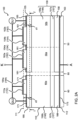
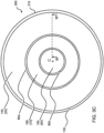
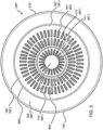
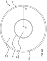
- Fig. 2A illustrates the power semiconductor device 100 in vertical cross-section along a line II-II' in Fig. 2B , which shows the power semiconductor 100 in top view, and along a line III-III' in Fig. 2C , which shows a horizontal cross-section of the power semiconductor device 100 along a line I-I' in Fig. 2A .
- the power semiconductor device 100 comprises a semiconductor wafer 110 having a first main side 111 and a second main side 112 opposite to the first main side 111.
- a thyristor structure 50 and a bipolar junction transistor (BJT) 60 are laterally separated from each other by an n-type separation region 80.
- first main side 111 and the second main side 112 of the semiconductor wafer 110 shall respectively be understood as a plane including the outermost flat surface portions of the semiconductor wafer 110 on two opposite sides.
- the thyristor structure 50 comprises in an order from the first main side 111 to the second main side 112 an n-type first emitter layer 154, a p-type first base layer 155, a n-type second base layer 159 and a p-type second emitter layer 158.
- the first emitter layer 154 is in direct contact with the first base layer 155 to form a first p-n junction between the first base layer 155 and the first emitter layer154
- the first base layer 155 is in direct contact with the second base layer 159 to form a second p-n junction between the first base layer 155 and the second base layer 159
- the second base layer 159 is in direct contact with the second emitter layer 158 to form a third p-n junction between the second base layer 159 and the second emitter layer 158.
- the second emitter layer 158 is separated from the first base layer 155 by the second base layer 159.
- the second base layer 159 comprises in an order from the first base layer 155 to the second emitter layer 158 a thyristor drift layer portion 156a and a thyristor buffer layer portion 157a.
- the thyristor drift layer portion 156a is in direct contact with the first base layer 155 and the thyristor buffer layer portion 157a is in direct contact with the second emitter layer 158.
- the thyristor buffer layer portion 157a is vertically separated from the first base layer 155 by the thyristor drift layer portion 156a.
- the thyristor structure 50 further comprises a gate electrode 161, a first main electrode 162 and a second main electrode 163.
- the gate electrode 161 is arranged lateral to the first emitter layer 154 and forms an ohmic contact with the first base layer 155
- the first main electrode 162 is arranged on the first main side 111 and forms an ohmic contact with the first emitter layer 154
- a second main electrode 163 is arranged on the second main side 112 and forms an ohmic contact with the second emitter layer 158.
- the BJT 60 is arranged lateral to the thyristor structure 50. It comprises a base electrode 171 electrically separated from the gate electrode 161, a third main electrode 172 arranged on the first main side 111 and a fourth main electrode 173 arranged on the second main side 112.
- the base electrode 171 corresponds to a base terminal of the BJT 60
- the third main electrode 172 corresponds to one of a collector terminal and an emitter terminal of the BJT 60
- the fourth main electrode 173 corresponds to the other one of the collector terminal and the emitter terminal of the BJT 60.
- the BJT 60 comprises in an order from the first main side 111 to the second main side 112 an n-type third emitter layer 184, a p-type third base layer 185, an n-type transistor drift layer portion 156b, an n-type transistor buffer layer portion 157b and an n-type collector layer 188.
- the third base layer 185 is connected to the third emitter layer 184 to form a fourth p-n junction
- the transistor drift layer portion 156b is connected to the third base layer 185 to form a fifth p-n junction
- the collector layer 188 is separated in a vertical direction (which is a direction extending from the first main side towards the second main side) from the transistor drift layer portion 156b by the transistor buffer layer portion 157b, i.e. the collector layer 188 is connected to the transistor drift layer 156b through the transistor buffer layer portion 157b.
- a drift layer 156 and a buffer layer 157 extend in the power semiconductor device 100 laterally throughout the whole semiconductor wafer 110. Accordingly, the drift layer 156 and the buffer layer 157 are shared by the thyristor structure 50, the BJT 60 and the separation region 80.
- the thyristor drift layer portion 156a is a first portion of the drift layer 156
- the transistor drift layer portion 156b is a second portion of the drift layer 156.
- the thyristor buffer layer portion 157a is a first portion of the buffer layer 157
- the transistor buffer layer portion 157b is a second portion of the buffer layer 157.
- a third portion of the drift layer 156 forms part of the separation region 80 and separates the thyristor drift layer portion 156a from the transistor drift layer portion 156b in a lateral direction.
- a third portion of the buffer layer forms part of the separation region 80 and separates the thyristor buffer layer portion 157a from the transistor buffer layer portion 157b in a lateral direction.
- the collector layer 188 and the buffer layer 157 both have a higher doping concentration than the drift layer 156.
- the buffer layer 157 may have a rising doping concentration towards the second main side 112, whereas the drift layer 156 has typically a constant doping concentration lower than that of the buffer layer 157.
- doping concentration refers to the net doping concentration.
- the doping concentration of a layer refers to a local doping concentration in case that a doping profile of this layer is described. If no doping profile is described, the doping concentration of a layer refers to the maximum doping concentration in this layer unless indicated otherwise.
- the third main electrode 172 forms an ohmic contact with the third emitter layer 184
- the fourth main electrode 173 forms an ohmic contact with the collector layer 188
- the base electrode 171 is arranged lateral to the third emitter layer 184 and forms an ohmic contact with the third base layer 185.
- the thyristor structure 50 comprises a gate commutated thyristor (GCT) device comprising a plurality of thyristor cells 50a and 50b.
- each thyristor cell 50a, 50b comprises a portion 154a, 154b of the first emitter layer 154, a portion of the first base layer 155, wherein the portion 154a, 154b of the first emitter layer 154 is in direct contact with the portion of the first base layer 155 to form a portion of the first p-n junction between the first base layer 155 and the first emitter layer 154, a portion of the second base layer 159, wherein the portion of the first base layer 155 is in direct contact with the portion of the second base layer 159 to form a portion of the second p-n junction between the first base layer 155 and the second base layer 159, and a portion of the second emitter layer 158 vertically separated from the portion of the first base layer 155 by the portion of the second base layer 159, where
- the thyristor structure 50 further comprises a portion of the gate electrode 161 which is arranged lateral to the portion 154a, 154b of the first emitter layer 154 and forms an ohmic contact with the portion of the first base layer 155, a portion 162a, 162b of the first main electrode 162 which forms an ohmic contact with the portion 154a, 154b of the first emitter layer 154, and a portion of the second main electrode 163 which forms an ohmic contact with the portion of the second emitter layer 158.
- the portion 154a, 154b of the first emitter layer 154 of each thyristor cell 50a, 50b is laterally separated from the portion 154a, 154b of the first emitter layer 154 of each other thyristor cell 50a, 50b.
- the portions 154a, 154b of the first emitter layer 154 are strip-shaped and arranged in two rings around a lateral center C of the circular semiconductor wafer 110.
- a longitudinal main axis of each strip-shaped portion 154a, 154b of the first emitter layer 154 is aligned along a radial direction extending from the lateral center C towards a circumferential edge region 130 of the semiconductor wafer 110.
- each strip-shaped portion 154a, 154b of the first emitter layer 154 is defined as an axis extending in the direction in which the strip-shaped portion 154a, 154b has its largest width.
- each strip-shaped portion 154a, 154b of the first emitter layer 154 and a corresponding strip-shaped portion 162a, 162b on top of the strip-shaped portion 154a, 154b is laterally surrounded by the gate electrode 161 implemented as continuous metallization layer.
- the gate electrode 161 On a lateral outer edge of the thyristor structure 50 the gate electrode 161 comprises a ring-shaped first common gate contact area 165 for connecting the gate electrode 161 to a later described first control unit GU1 as schematically shown in Fig. 2A .
- the BJT 60 has a cell structure with a plurality of BJT cells 60a wherein all of the plurality of BJT cells 60a have a same basic structure.
- Fig. 2A shows one of the plurality of BJT cells 60a in cross-section. In Fig. 2B this BJT cell 60a is indicated by a dashed line.
- each BJT cell 60a comprises a portion of the base electrode 171, a strip-shaped portion 172a of the third main electrode 172 and a portion of the fourth main electrode 173.
- the portion of the base electrode 171 corresponds to a base terminal of the BJT cell 60a
- the portion 172a of the third main electrode 172 corresponds to one of a collector terminal and an emitter terminal of the BJT cell 60a
- the portion of the fourth main electrode 173 corresponds to the other one of the collector terminal and the emitter terminal of the BJT cell 60a.
- the BJT cell 60a further comprises in an order from the first main side 111 to the second main side 112 a strip-shaped portion 184a of the third emitter layer 184, a portion of the third base layer 185, a portion of the transistor drift layer portion 156b, a portion of the transistor buffer layer portion 157b and a portion of the collector layer 188.
- the portion of the third base layer 185 is connected to the portion of the third emitter layer 184 to form a portion of the fourth p-n junction
- the portion of the transistor drift layer portion 156b is connected to the portion of the third base layer 185 to form a portion of the fifth p-n junction
- the portion of the collector layer 188 is separated in a vertical direction (which is a direction extending from the first main side towards the second main side) from the portion of the transistor drift layer portion 156b by the portion of the transistor buffer layer portion 157b, i.e. the portion of the collector layer 188 is connected to the portion of the transistor drift layer portion 156b through the portion of the transistor buffer layer portion 157b.
- the base electrode 162 comprises a circular shaped second common gate contact area 175 for connecting the base electrode 171 to a later described second control unit GU1 as schematically shown in Fig. 2A .
- a depth d1 of the first base layer 155, to which depth d1 the first base layer 155 extends from the first main side 111 is the same as a depth d2 of the third base layer 185, to which depth d2 the third base layer 185 extends from the first main side 111 (i.e. the depth d2 of the third base layer 185 is to be understood as a maximum distance between the first main side 111 and a point within the third base layer 185).
- the first base layer 155 may have, at a first lateral position at which a lateral gradient of a doping concentration of the first base layer 155 is zero for all vertical positions, the same vertical doping concentration profile as the third base layer 185 at a second lateral position at which a lateral gradient of a doping concentration of the third base layer 185 is zero for all vertical positions.
- a ratio between a BJT area and a thyristor area may be in a range between 0.1 and 0.3, or in a range between 0.15 and 0.25, wherein the thyristor area is defined as an area occupied by the first base layers 155 of the thyristor structure 50 in a horizontal projection onto a plane parallel to the second main side 112 and wherein the BJT area is defined as an area occupied by the third base layer 185 in the horizontal projection onto the plane parallel to the second main side 112.
- the first main electrode 162 is electrically connected to the third main electrode 172 and the second main electrode 163 is electrically connected to the fourth main electrode 173.
- the first main electrode 162 and the second main electrode 163 are both electrically connected to a cathode terminal K of the power semiconductor device 100
- the second main electrode 163 and the fourth main electrode 173 are both electrically connected to an anode terminal A of the power semiconductor device 100.
- the first control unit GU1 which is electrically connected to the gate electrode 161, is configured to control a voltage and/or current applied to the gate electrode 161, while the second control unit GU2, which is electrically connected to the base electrode 171, is electrically configured to control a current and/or voltage applied to the base electrode 171.
- the first control unit GU1 and the second control unit GU2 are configured to first turn on the BJT 60 in a state in which the thyristor structure 50 is in a forward blocking state, to thereafter turn on the thyristor structure 50 from the forward blocking state into the forward conducting state, and to thereafter turn off the bipolar junction transistor 60 while maintaining the thyristor structure 50 in the forward conducting state.
- control of the thyristor structure 50 and of the BJT 60 turn-on of the thyristor structure 50 can be performed in a safe manner without using additional protection circuits.
- Fig. 3A illustrates the power semiconductor device 100 in vertical cross-section along a line II-II' in Fig. 3B , which shows the power semiconductor 100 in top view, and along a line III-III' in Fig. 2C , which shows a horizontal cross-section of the power semiconductor device 100 along a line I-I' in Fig. 3A .
- a description of the power semiconductor device 200 will focus on differences whereas it is referred to the above description of the first embodiment with regard to all remaining features.
- elements having the same reference signs in the Figs. 2A-2C and Figs. 3A to 3C shall have the same features if not indicated otherwise.
- the power semiconductor device 200 according to the second embodiment differs from the power semiconductor device 100 according to the first embodiment in that it comprises in a semiconductor wafer 210 having a first main side 211 and a second main side 212 in addition to the thyristor structure 50 and the BJT 60 a freewheeling diode structure 90 integrated in the semiconductor wafer 210.
- the freewheeling diode structure 90 comprises in an order from the first main side 211 to the second main side a p-type first diode layer 191, an n-type diode drift layer portion 156c, an n-type diode buffer layer portion 157c and an n-type diode cathode layer 192a.
- the n-type diode drift layer portion 156c, the n-type diode buffer layer portion 157c and the n-type diode cathode layer 192a form an n-type second diode layer.
- a p-n junction is formed between the n-type drift layer portion 156c and the first diode layer 191, i.e. between the first diode layer 191 and the second diode layer 192.
- the freewheeling diode structure 90 is ring-shaped and arranged laterally between the thyristor structure 50 and the BJT 60.
- a separation region 80 is arranged between the thyristor structure 50 and the BJT 60
- a first separation region 80a is laterally interposed between the freewheeling diode structure 90 and the thyristor structure 50
- a second separation region 80b is laterally interposed between the freewheeling diode structure 90 and the BJT 60.
- the first separation region 80a and the second separation region 80b separate the thyristor structure 50 from the BJT 60.
- Each of the first separation region 80a and the second separation region 80b may have a similar structure as the separation region 80 in the first embodiment.
- Each one of the first separation region 80a and the second separation region 80b is a separation region as defined in the claims.
- the drift layer 156 and the buffer layer 157 extend laterally through the whole semiconductor wafer 210 as in the first embodiment.
- the thyristor drift layer portion 156a is a first portion of the drift layer 156 and the transistor drift layer portion 156b is a second portion of the drift layer 156.
- the diode drift layer portion 156c is a third portion of the drift layer 156, and the first separation region 80a and the second separation region 80b include a fourth and fifth portion of the drift layer 156, respectively.
- the thyristor buffer layer portion 157a is a first portion of the buffer layer 157
- the transistor buffer layer portion 157b is a second portion of the buffer layer 157.
- the diode buffer layer portion 157c is a third portion of the buffer layer 157, and the first separation region 80a and the second separation region 80b include a fourth and fifth portion of the buffer layer 157, respectively.
- a power semiconductor device 200' according to a third embodiment is described with reference to Fig. 4 , which shows a top view of the power semiconductor device 200'. Due to many similarities between the power semiconductor device 200 according to the second embodiment and the power semiconductor device 200' according to the third embodiment, a description of the power semiconductor device 200' will focus on differences, whereas it is referred to the above description of the second embodiment with regard to all remaining features. In particular, elements having having reference signs with the same reference numerals in Figs. 3A to 3C and Fig. 4 shall have the same features and characteristics if not indicated otherwise.
- the power semiconductor device 200' differs from power semiconductor device 200 only in a different arrangement of the freewheeling diode structure 90' relative to the thyristor structure 50' and the BJT 60' in a semiconductor wafer 210'.
- the thyristor structure 50', the BJT 60' and the freewheeling diode structure 90' look respectively the same as the thyristor structure 50, the BJT 60 and the freewheeling diode structure 90 in the second embodiment described above.
- the freewheeling diode structure 90 is arranged laterally between the outer thyristor structure 50' and the central BJT 60', the freewheeling diode 90' in the power semiconductor device 200' is arranged in the lateral center region of the semiconductor wafer 210', and the BJT 60' is laterally arranged between the thyristor structure 50' adjacent to an circumferential edge region 130' of the semiconductor wafer 210' and the central freewheeling diode structure 90'.
- the second common gate contact area 165 is laterally arranged in a central region of the BJT 60
- a second common gate contact area 165' is laterally arranged at an outer circumferential edge of the BJT 60'.
- a first separation region 80a' is interposed between the central freewheeling diode structure 90' and the BJT 60', and a second separation region 80b' is interposed between the BJT 60 and the outer thyristor structure 50'.
- the first separation region 80a' and the second separation region 80b' have in cross-section the same structure than the first separation region 80a and the second separation region 80b in the second embodiment but are interposed between different entities.
- the second separation region 80b' is a separation region as defined in the claims.
- a power semiconductor device 200" according to a fourth embodiment is described with reference to Fig. 5 , which shows a top view of the power semiconductor device 200". Due to many similarities between the power semiconductor device 200 according to the second embodiment and the power semiconductor device 200" according to the fourth embodiment, a description of the power semiconductor device 200" will focus on differences, whereas it is referred to the above description of the second embodiment with regard to all remaining features. In particular, elements having reference signs with the same reference numerals in Figs. 3A to 3C and Fig. 5 shall have the same features and characteristics if not indicated otherwise.
- the power semiconductor device 200" differs from power semiconductor device 200 only in a different arrangement of the freewheeling diode structure 90" relative to the thyristor structure 50" and the BJT 60" in a semiconductor wafer 210".
- the thyristor structure 50", the BJT 60" and the freewheeling diode structure 90" look respectively substantially the same as the thyristor structure 50, the BJT 60 and the freewheeling diode structure 90 in the second embodiment described above.
- the freewheeling diode structure 90 is arranged laterally between the outer thyristor structure 50 and the central BJT 60
- the freewheeling diode 90' in the power semiconductor device 200' is arranged adjacent to the circumferential edge region 130" of the semiconductor wafer 210" to surround both the BJT 60" and the thyristor structure 50".
- the BJT 60" is laterally arranged between the outer freewheeling diode structure 90" and the thyristor structure 50" in the lateral center region of the semiconductor wafer 210".
- a first separation region 80a" is laterally interposed between the central BJT 60" and the thyristor structure 50", and a second separation region 80b" is laterally interposed between the thyristor structure 50" and the freewheeling diode structure 90".
- the first separation region 80a" and the second separation region 80b" have in cross-section the same structure than the first separation region 80a and the second separation region 80b in the second embodiment but are interposed between different entities.
- the first separation region 80a" is a separation region as defined in the claims.
- Fig. 6A illustrates the power semiconductor device 300 in vertical cross-section along a line II-II' in Fig. 6B , which shows the power semiconductor 300 in top view.
- the cross-section shown in Fig. 6A is also a cross-section along a line III-III' in Fig. 6C , which shows a horizontal cross-section of the power semiconductor device 100 along a line I-I' in Fig. 6A , and is a cross-section along a line IV-IV' in Fig. 6D , which shows a horizontal cross-section of the power semiconductor device 300 along a line V-V' in Fig. 6A .
- the power semiconductor device 300 comprises a semiconductor wafer 310 having a first main side 311 and a second main side 312. It comprises a thyristor structure 50, a BJT 360 and a separation region 80 laterally interposed between the thyristor structure 50 and the BJT 360.
- the power semiconductor device 300 differs from the power semiconductor device 100 in that the BJT 360 has a different structure than the BJT 60 in the first embodiment.
- the BJT 360 comprises a base electrode 371 electrically separated from the gate electrode 171, a third main electrode 372 arranged on the first main side 311and a fourth main electrode 373 arranged on the second main side 312.
- the base electrode 371 corresponds to a base terminal of the bipolar junction transistor 360
- the third main electrode 372 corresponds to a collector terminal of the bipolar junction transistor 360
- the fourth main electrode 373 corresponds to an emitter terminal of the bipolar junction transistor 360.
- the BJT 360 comprises in the semiconductor wafer 310 a p-type collector layer 388 arranged adjacent to the first main side 311, an n-type third base layer 385 arranged adjacent to the second main side 312, a p-type third emitter layer 384 arranged adjacent to the second main side 312 lateral to the third base layer 385, an n-type transistor drift layer portion 156b, and an n-type transistor buffer layer portion 157b.
- the transistor drift layer portion 156b and the transistor buffer layer portion 157b are both arranged between the collector layer 388 and each one of the third base layer 384 and the third emitter layer 385, wherein the collector layer 388 is connected to the drift layer 156 through a fourth p-n junction, the third base layer 385 is connected to the drift layer 156 through the buffer layer 157, and the third base layer 385 is connected to the third emitter layer through a fifth p-n junction.
- the third main electrode 372 forms an ohmic contact with the collector layer 388
- the fourth main electrode 371 forms an ohmic contact with the third emitter layer 384
- the base electrode 371 is arranged lateral to the fourth main electrode 373 and forms an ohmic contact with the third base layer 385.
- the collector layer 188 comprises in an order from the first main side 311 towards the second main side 312 a first collector layer portion 88a and a second collector layer portion 88b, wherein the second collector layer portion 88b has along a vertical direction a similar doping profile than the first base layer 155 along a vertical direction.
- a depth d1 of the first base layer 155 to which the first base layer 155 extends from the first main side 311 may be the same as a depth d3 of the collector layer 388 to which the second collector layer portion 88b of the collector layer 388 extends from the first main side 311.
- a depth d4 of the second emitter layer 158 to which the second emitter layer 158 extends from the second main side 312 is the same as a depth d5 of the third emitter layer 384 to which the third emitter layer 384 extends from the second main side 312.
- the thyristor structure 50, 50', 50", of the BJT 60, 60', 60", 360 and the freewheeling diode 90, 90', 90" have been described. However, other lateral arrangements are possible. Also, the invention is not limited to a specific cell structure of the thyristor structure 50, 50', 50" and of the BJT 60, 60', 60", 360. Moreover, while the freewheeling diode 90, 90', 90" was described with a single continuous first diode layer 291 and a single continuous second diode layer 292, the freewheeling diode may have any other segmented cell structure.
- the semiconductor wafer of the power semiconductor device of the invention may be made of silicon (Si) or any other appropriate semiconductor material.
- first control unit (GU1) and the second control unit (GU2) may be implemented in one single control unit, which has the functionality of both control units GU1 and GU2.
Landscapes
- Thyristors (AREA)
- Bipolar Transistors (AREA)
- Metal-Oxide And Bipolar Metal-Oxide Semiconductor Integrated Circuits (AREA)
Claims (12)
- Leistungshalbleiterbauelement, Folgendes umfassend:einen Halbleiter-Wafer (110; 210; 210'; 210"; 310) mit einer ersten Hauptseite (111; 211; 311) und einer zweiten Hauptseite (112; 212; 312), die der ersten Hauptseite (111; 211; 311) entgegengesetzt ist; undeine Thyristorstruktur (50; 50'; 50"), die in einer Reihenfolge von der ersten Hauptseite (111; 211; 311) zu der zweiten Hauptseite (112; 212; 312) Folgendes umfasst:• eine erste Emitterschicht (154) eines ersten Leitfähigkeitstyps;• eine erste Basisschicht (155) eines zweiten Leitfähigkeitstyps, der von dem ersten Leitfähigkeitstyp verschieden ist, wobei die erste Emitterschicht (154) in unmittelbarem Kontakt mit der ersten Basisschicht (155) steht, um einen ersten p-n-Übergang zwischen der ersten Basisschicht (155) und der ersten Emitterschicht (154) auszubilden;• eine zweite Basisschicht (159) des ersten Leitfähigkeitstyps, wobei die erste Basisschicht (155) in unmittelbarem Kontakt mit der zweiten Basisschicht (159) steht, um einen zweiten p-n-Übergang zwischen der ersten Basisschicht (155) und der zweiten Basisschicht (159) auszubilden; und• eine zweite Emitterschicht (158) des zweiten Leitfähigkeitstyps, die durch die zweite Basisschicht (159) von der ersten Basisschicht (155) separiert ist, wobei die zweite Basisschicht (159) in unmittelbarem Kontakt mit der zweiten Emitterschicht (158) steht, um einen dritten p-n-Übergang zwischen der zweiten Basisschicht (159) und der zweiten Emitterschicht (158) auszubilden,wobei die Thyristorstruktur (50; 50'; 50") weiterhin Folgendes umfasst:• eine Gate-Elektrode (161), die lateral zu der ersten Emitterschicht (154) angeordnet ist und mit der ersten Basisschicht (155) einen ohmschen Kontakt ausbildet;• eine erste Hauptelektrode (162), die auf der ersten Hauptseite (111; 211; 311) angeordnet ist und mit der ersten Emitterschicht (154) einen ohmschen Kontakt ausbildet; und• eine zweite Hauptelektrode (163), die auf der zweiten Hauptseite (112; 212; 312) angeordnet ist und mit der zweiten Emitterschicht (158) einen ohmschen Kontakt ausbildet,wobei das Leistungshalbleiterbauelement weiterhin einen Bipolartransistor (60; 60'; 60"; 360) umfasst, der lateral zu der Thyristorstruktur (50; 50'; 50") angeordnet ist,wobei der Bipolartransistor (60; 60'; 60"; 360) eine Basiselektrode (171; 171'; 171"; 371), die elektrisch von der Gate-Elektrode (161) separiert ist, eine dritte Hauptelektrode (172; 172'; 172"; 372), die auf der ersten Hauptseite (111; 211; 311) angeordnet ist, und eine vierte Hauptelektrode (173; 373) umfasst, die auf der zweiten Hauptseite (112; 212; 312) angeordnet ist,wobei die Basiselektrode (171; 171'; 171"; 371) einem Basisanschluss des Bipolartransistors (60; 60'; 60"; 360) entspricht, undwobei die dritte Hauptelektrode (172; 172'; 172"; 372) einem von einem Kollektoranschluss und einem Emitteranschluss des Bipolartransistors (60; 60'; 60"; 360) entspricht und die vierte Hauptelektrode (173; 373) dem anderen des Kollektoranschlusses und des Emitteranschlusses des Bipolartransistors (60; 60'; 60"; 360) entspricht,dadurch gekennzeichnet, dass die erste Hauptelektrode (162; 162'; 162") elektrisch mit der dritten Hauptelektrode (172; 172'; 172"; 372) verbunden ist und die zweite Hauptelektrode (163) elektrisch mit der vierten Hauptelektrode (173; 373) verbunden ist,wobei die Thyristorstruktur (50; 50'; 50") ein Gatekommutiertes Thyristor-(GCT)-Bauelement umfasst, das mehrere Thyristorzellen (50a, 50b) umfasst,wobei jede Thyristorzelle (50a, 50b) Folgendes umfasst• einen Abschnitt (154a, 154b) der ersten Emitterschicht (154);• einen Abschnitt der ersten Basisschicht (155), wobei der Abschnitt (154a, 154b) der ersten Emitterschicht (154) in unmittelbarem Kontakt mit dem Abschnitt der ersten Basisschicht (155) steht, um einen Abschnitt des ersten p-n-Übergangs zwischen der ersten Basisschicht (155) und der ersten Emitterschicht (154) auszubilden;• einen Abschnitt der zweiten Basisschicht (159), wobei der erste Abschnitt der ersten Basisschicht (155) in unmittelbarem Kontakt mit dem Abschnitt der zweiten Basisschicht (159) steht, um einen Abschnitt des zweiten p-n-Übergangs zwischen der ersten Basisschicht (155) und der zweiten Basisschicht (159) auszubilden; und• einen Abschnitt der zweiten Emitterschicht (158), der durch die zweite Basisschicht (159) von dem Abschnitt der ersten Basisschicht (155) separiert ist, wobei der Abschnitt der zweiten Basisschicht (159) in unmittelbarem Kontakt mit dem Abschnitt der zweiten Emitterschicht (158) steht, um einen Abschnitt des dritten p-n-Übergangs zwischen der zweiten Basisschicht (159) und der zweiten Emitterschicht (158) auszubilden,wobei die Thyristorstruktur (50; 50'; 50") weiterhin Folgendes umfasst:• einen Abschnitt der Gate-Elektrode (161), die lateral zu dem Abschnitt (154a, 154b) der ersten Emitterschicht (154) angeordnet ist und mit dem Abschnitt der ersten Basisschicht (155) einen ohmschen Kontakt ausbildet;• einen Abschnitt (162a, 162b) der ersten Hauptelektrode (162), die mit dem Abschnitt (154a, 154b) der ersten Emitterschicht (154) einen ohmschen Kontakt ausbildet; und• einen Abschnitt der zweiten Hauptelektrode (163), die mit dem Abschnitt der zweiten Emitterschicht (158) einen ohmschen Kontakt ausbildet, undwobei der Abschnitt (154a, 154b) der ersten Emitterschicht (154) jeder Thyristorzelle (50a, 50b) lateral von dem Abschnitt (154a, 154b) der ersten Emitterschicht (154) jeder anderen Thyristorzelle (50a, 50b) separiert ist.
- Leistungshalbleiterbauelement nach Anspruch 1, wobei der Halbleiter-Wafer (110; 210; 210'; 210"; 310) einen Separierungsbereich (80; 80a, 80b; 80b'; 80a") des ersten Leitfähigkeitstyps umfasst, wobei der Separierungsbereich (80; 80a, 80b; 80b'; 80a") lateral zwischen dem Bipolartransistor (60; 60'; 60"; 360) und der Thyristorstruktur (50; 50'; 50") angeordnet ist, um den Bipolartransistor (60; 60'; 60"; 360) durch mindestens den Separierungsbereich (80; 80a, 80b) von der Thyristorstruktur (50; 50'; 50") zu separieren.
- Leistungshalbleiterbauelement nach einem der vorhergehenden Ansprüche, wobei der Halbleiter-Wafer (210; 210; 210") eine Freilaufdiode (90; 90'; 90") umfasst, die lateral zu der Thyristorstruktur (50; 50'; 50") angeordnet ist und lateral zu dem Bipolartransistor (60; 60'; 60") angeordnet ist, wobei die Freilaufdiode (90; 90'; 90") in einer Reihenfolge von der ersten Hauptseite (211) zu der zweiten Hauptseite (212) eine erste Diodenschicht (191) des zweiten Leitfähigkeitstyps und eine zweite Diodenschicht (192) des ersten Leitfähigkeitstyps umfasst, die einen vierten p-n-Übergang mit der ersten Diodenschicht (191) ausbildet.
- Leistungshalbleiterbauelement nach einem der vorhergehenden Ansprüche, wobei die zweite Basisschicht (159) einen relativ gering dotierten Thyristordriftschichtabschnitt (156a) und einen Thyristorpufferschichtabschnitt (157a) umfasst, der eine höhere Dotierungskonzentration als die des Thyristordriftschichtabschnitts (156a) aufweist, wobei der Thyristorpufferschichtabschnitt (157a) den Thyristordriftschichtabschnitt (156a) von der zweiten Emitterschicht (158) separiert.
- Leistungshalbleiterbauelement nach einem der vorhergehenden Ansprüche, wobei der Bipolartransistor (60; 60'; 60") in einer Reihenfolge von der ersten Hauptseite (111; 211) zu der zweiten Hauptseite (112; 212) Folgendes umfasst:• eine dritte Emitterschicht (184) des ersten Leitfähigkeitstyps;• eine dritte Basisschicht (185) des zweiten Leitfähigkeitstyps, die durch einen vierten p-n-Übergang mit der dritten Emitterschicht (184) verbunden ist;• einen Transistordriftschichtabschnitt (156b) des ersten Leitfähigkeitstyps, der durch einen fünften p-n-Übergang mit der dritten Basisschicht (185) verbunden ist; und• eine Kollektorschicht (188) des ersten Leitfähigkeitstyps, die eine höhere Dotierungskonzentration als der Transistordriftschichtabschnitt (156b) aufweist und entweder in unmittelbarem Kontakt mit dem Transistordriftschichtabschnitt (156b) steht oder durch einen Transistorpufferschichtabschnitt (157b) des ersten Leitfähigkeitstyps mit dem Transistordriftschichtabschnitt (156b) verbunden ist, wobei der Transistorpufferschichtabschnitt (157b) eine höhere Dotierungskonzentration als die des Transistordriftschichtabschnitts (156b) aufweist,wobei die dritte Hauptelektrode (172; 172'; 172") mit der dritten Emitterschicht (184) einen ohmschen Kontakt ausbildet,wobei die vierte Hauptelektrode (173) mit der Kollektorschicht (188) einen ohmschen Kontakt ausbildet undwobei die Basiselektrode (171; 171'; 171") lateral zu der dritten Emitterschicht (184) angeordnet ist und mit der dritten Basisschicht (185) einen ohmschen Kontakt ausbildet.
- Leistungshalbleiterbauelement nach Anspruch 5, wobei eine Tiefe (d1) der ersten Basisschicht (155), auf die sich die erste Basisschicht (155) von der ersten Hauptseite (111; 211) erstreckt, die gleiche ist wie eine Tiefe (d2) der dritten Basisschicht (185), auf die sich die dritte Basisschicht (185) von der ersten Hauptseite (111; 211) erstreckt.
- Leistungshalbleiterbauelement nach Anspruch 6, wobei die erste Basisschicht (155) an einer ersten lateralen Position, an der ein lateraler Gradient einer Dotierungskonzentration der ersten Basisschicht (155) für alle vertikalen Positionen null ist, das gleiche vertikale Dotierungskonzentrationsprofil wie die dritte Basisschicht (185) an einer zweiten lateralen Position aufweist, an der ein lateraler Gradient einer Dotierungskonzentration der dritten Basisschicht (185) für alle vertikalen Positionen null ist.
- Leistungshalbleiterbauelement nach einem der Ansprüche 5 bis 7, wobei ein Verhältnis zwischen einer Bipolartransistorfläche und einer Thyristorfläche in einem Bereich zwischen 0,1 und 0,3 oder in einem Bereich zwischen 0,15 und 0,25 ist, wobei die Thyristorfläche als eine Fläche definiert ist, die von den ersten Basisschichten (155) der Thyristorstruktur (50; 50'; 50") in einer horizontalen Projektion auf eine Ebene parallel zu der zweiten Hauptseite (112; 212) belegt ist, und wobei die Bipolartransistorfläche als eine Fläche definiert ist, die von der dritten Basisschicht (185) in der horizontalen Projektion auf die Ebene parallel zu der zweiten Hauptseite (112; 212) belegt ist.
- Leistungshalbleiterbauelement nach einem der Ansprüche 1 bis 4, wobei der Bipolartransistor (360) Folgendes umfasst:• eine Kollektorschicht (388) des zweiten Leitfähigkeitstyps, die der ersten Hauptseite (311) benachbart angeordnet ist;• eine dritte Basisschicht (385) des ersten Leitfähigkeitstyps, die der zweiten Hauptseite (312) benachbart angeordnet ist;• eine dritte Emitterschicht (384) des zweiten Leitfähigkeitstyps, die der zweiten Hauptseite (312) benachbart lateral zu der dritten Basisschicht (385) angeordnet ist; und• einen Transistordriftschichtabschnitt (156b), der zwischen der Kollektorschicht (388) und jeweils einer der dritten Basisschicht (384) und der dritten Emitterschicht (385) angeordnet ist,wobei die Kollektorschicht (388) durch einen vierten p-n-Übergang mit dem Transistordriftschichtabschnitt (156b) verbunden ist,wobei die dritte Basisschicht (385) entweder in unmittelbarem Kontakt mit dem Transistordriftschichtabschnitt (156b) steht oder durch einen Transistorpufferschichtabschnitt (157b) des ersten Leitfähigkeitstyps mit dem Transistordriftschichtabschnitt (156b) verbunden ist, wobei der Transistorpufferschichtabschnitt (157b) eine höhere Dotierungskonzentration aufweist als die des Transistordriftschichtabschnitts (156b),wobei die dritte Basisschicht (385) durch einen fünften p-n-Übergang mit der dritten Emitterschicht (384) verbunden ist,wobei die dritte Hauptelektrode (372) mit der Kollektorschicht (388) einen ohmschen Kontakt ausbildet,wobei die vierte Hauptelektrode (371) mit der dritten Emitterschicht (384) einen ohmschen Kontakt ausbildet undwobei die Basiselektrode (371) lateral zu der vierten Hauptelektrode (373) angeordnet ist und mit der dritten Basisschicht (385) einen ohmschen Kontakt ausbildet.
- Leistungshalbleiterbauelement nach Anspruch 9, wobei eine Tiefe (d1) der ersten Basisschicht (155), auf die sich die erste Basisschicht (155) von der ersten Hauptseite (311) erstreckt, die gleiche ist wie eine Tiefe (d3) der Kollektorschicht (388), auf die sich die Kollektorschicht (388) von der ersten Hauptseite (311) erstreckt.
- Leistungshalbleiterbauelement nach Anspruch 9 oder 10, wobei eine Tiefe (d4) der zweiten Emitterschicht (158), auf die sich die zweiten Emitterschicht (158) von der zweiten Hauptseite (312) erstreckt, die gleiche ist wie eine Tiefe (d5) der dritten Emitterschicht (384), auf die sich die dritte Emitterschicht (384) von der zweiten Hauptseite (312) erstreckt.
- Leistungshalbleiterbauelement nach einem der Ansprüche 1 bis 11, Folgendes umfassend:eine erste Steuerungseinheit (GU1), die elektrisch mit der Gate-Elektrode (161; 161'; 161") verbunden ist und eingerichtet ist, um eine Spannung und/oder einen Strom zu steuern, die an die Gate-Elektrode (161; 161'; 161") angelegt werden; undeine zweite Steuerungseinheit (GU2), die elektrisch eingerichtet ist, um einen Strom und/oder eine Spannung zu steuern, die an die Basiselektrode (171; 171'; 171"; 371) angelegt werden,wobei die erste Steuerungseinheit (GU1) und die zweite Steuerungseinheit (GU2) eingerichtet sind, um zuerst den Bipolartransistor (60; 60'; 60"; 360) in einem Zustand einzuschalten, in dem die Thyristorstruktur (50; 50'; 50") in einem Sperrzustand in Vorwärtsrichtung ist, um danach die Thyristorstruktur (50; 50'; 50") aus dem Sperrzustand in Vorwärtsrichtung in den Durchlasszustand in Vorwärtsrichtung einzuschalten, und um danach den Bipolartransistor (60; 60'; 60"; 360) auszuschalten, während die Thyristorstruktur (50; 50'; 50") in dem Durchlasszustand in Vorwärtsrichtung gehalten wird.
Applications Claiming Priority (2)
| Application Number | Priority Date | Filing Date | Title |
|---|---|---|---|
| EP20167336 | 2020-03-31 | ||
| PCT/EP2021/055919 WO2021197774A1 (en) | 2020-03-31 | 2021-03-09 | Power semiconductor device comprising a thyristor and a bipolar junction transistor |
Publications (3)
| Publication Number | Publication Date |
|---|---|
| EP4128359A1 EP4128359A1 (de) | 2023-02-08 |
| EP4128359B1 true EP4128359B1 (de) | 2023-11-08 |
| EP4128359B8 EP4128359B8 (de) | 2023-12-20 |
Family
ID=70110216
Family Applications (1)
| Application Number | Title | Priority Date | Filing Date |
|---|---|---|---|
| EP21709708.8A Active EP4128359B8 (de) | 2020-03-31 | 2021-03-09 | Leistungshalbleiterbauelement mit einem thyristor and einem bipolartransistor |
Country Status (5)
| Country | Link |
|---|---|
| US (1) | US12148818B2 (de) |
| EP (1) | EP4128359B8 (de) |
| JP (1) | JP7432098B2 (de) |
| CN (1) | CN115380388A (de) |
| WO (1) | WO2021197774A1 (de) |
Families Citing this family (1)
| Publication number | Priority date | Publication date | Assignee | Title |
|---|---|---|---|---|
| WO2024217675A1 (en) | 2023-04-19 | 2024-10-24 | Hitachi Energy Ltd | Fully controllable, power semiconductor switching assembly, power semiconductor device, snubber-less power converter and method for manufacturing |
Family Cites Families (11)
| Publication number | Priority date | Publication date | Assignee | Title |
|---|---|---|---|---|
| US3265909A (en) | 1963-09-03 | 1966-08-09 | Gen Electric | Semiconductor switch comprising a controlled rectifier supplying base drive to a transistor |
| FR2536909A1 (fr) | 1982-11-25 | 1984-06-01 | Centre Nat Rech Scient | Structure de thyristor a allumage intrinseque et son application a la realisation d'un dispositif bidirectionnel |
| FR2566963B1 (fr) * | 1984-06-29 | 1987-03-06 | Silicium Semiconducteur Ssc | Triac de protection sans gachette, realise a partir d'un substrat a haute resistivite |
| GB9127476D0 (en) | 1991-12-30 | 1992-02-19 | Texas Instruments Ltd | A semiconductor integrated circuit |
| KR0127282B1 (ko) | 1992-05-18 | 1998-04-02 | 도요다 요시또시 | 반도체 장치 |
| FR2726398B1 (fr) * | 1994-10-28 | 1997-01-17 | Sgs Thomson Microelectronics | Thyristor commandable par des niveaux logiques |
| EP1049175B1 (de) | 1998-11-11 | 2009-09-02 | Mitsubishi Denki Kabushiki Kaisha | Rückwärtsleitender thyristor, halbleiteranordnung mit mechanischem kontakt und halbleitersubstrat |
| EP2622639B1 (de) | 2010-09-29 | 2015-01-21 | ABB Technology AG | Rückwärtsleitendes hochleistungshalbleiterbauelement |
| WO2016096956A1 (en) | 2014-12-17 | 2016-06-23 | Abb Technology Ag | Bidirectional power semiconductor device |
| EP3073530B1 (de) | 2015-03-23 | 2017-05-03 | ABB Schweiz AG | Rückwärtsleitendes hochleistungshalbleiterbauelement |
| CN106847810A (zh) * | 2016-12-27 | 2017-06-13 | 湖南大学 | Bjt辅助的改进型gto结构、控制方法及制备方法 |
-
2021
- 2021-03-09 CN CN202180026333.XA patent/CN115380388A/zh active Pending
- 2021-03-09 JP JP2022559655A patent/JP7432098B2/ja active Active
- 2021-03-09 US US17/913,981 patent/US12148818B2/en active Active
- 2021-03-09 WO PCT/EP2021/055919 patent/WO2021197774A1/en not_active Ceased
- 2021-03-09 EP EP21709708.8A patent/EP4128359B8/de active Active
Also Published As
| Publication number | Publication date |
|---|---|
| JP7432098B2 (ja) | 2024-02-16 |
| CN115380388A (zh) | 2022-11-22 |
| JP2023519984A (ja) | 2023-05-15 |
| WO2021197774A1 (en) | 2021-10-07 |
| EP4128359A1 (de) | 2023-02-08 |
| EP4128359B8 (de) | 2023-12-20 |
| US20230118951A1 (en) | 2023-04-20 |
| US12148818B2 (en) | 2024-11-19 |
Similar Documents
| Publication | Publication Date | Title |
|---|---|---|
| US5702961A (en) | Methods of forming insulated gate bipolar transistors having built-in freewheeling diodes and transistors formed thereby | |
| US6724043B1 (en) | Bipolar MOSFET device | |
| JP3141769B2 (ja) | 絶縁ゲート型サイリスタ及びその製造方法 | |
| US8420454B2 (en) | Three-terminal power device with high switching speed and manufacturing process | |
| JP4185157B2 (ja) | 半導体素子及び電気機器 | |
| EP2622639B1 (de) | Rückwärtsleitendes hochleistungshalbleiterbauelement | |
| JP4167294B2 (ja) | 半導体素子及び電気機器 | |
| EP3235003B1 (de) | Bidirektionale leistungshalbleitervorrichtung | |
| EP3987661B1 (de) | Entwurf einer vorrichtung zum kurzschlussschutz von transistoren | |
| US12432988B2 (en) | Semiconductor device including substrate layer with floating base region and gate driver circuit | |
| EP3087607B1 (de) | Rückwärtsleitendes halbleiterbauelement | |
| US5936267A (en) | Insulated gate thyristor | |
| JP2002532885A (ja) | 出力半導体回路 | |
| US5757034A (en) | Emitter switched thyristor | |
| US12148818B2 (en) | Power semiconductor device comprising a thyristor and a bipolar junction transistor | |
| US5614738A (en) | Insulated gate thyristor having a polysilicon resistor connected to its base | |
| US20250220982A1 (en) | Monolithic bidirectional jfet switch | |
| US5296725A (en) | Integrated multicelled semiconductor switching device for high current applications | |
| US5684306A (en) | Insulated gate thyristor | |
| US4825270A (en) | Gate turn-off thyristor | |
| JP2777990B2 (ja) | 自己消弧形サイリスタ | |
| JPH098280A (ja) | 半導体装置及びそれを用いたインバータ装置 | |
| CN115336002A (zh) | 具有栅极流道的关断功率半导体装置 | |
| JPH08241980A (ja) | 絶縁ゲート型サイリスタ | |
| JP2000012832A (ja) | 静電誘導サイリスタ |
Legal Events
| Date | Code | Title | Description |
|---|---|---|---|
| STAA | Information on the status of an ep patent application or granted ep patent |
Free format text: STATUS: UNKNOWN |
|
| STAA | Information on the status of an ep patent application or granted ep patent |
Free format text: STATUS: THE INTERNATIONAL PUBLICATION HAS BEEN MADE |
|
| PUAI | Public reference made under article 153(3) epc to a published international application that has entered the european phase |
Free format text: ORIGINAL CODE: 0009012 |
|
| STAA | Information on the status of an ep patent application or granted ep patent |
Free format text: STATUS: REQUEST FOR EXAMINATION WAS MADE |
|
| 17P | Request for examination filed |
Effective date: 20220930 |
|
| AK | Designated contracting states |
Kind code of ref document: A1 Designated state(s): AL AT BE BG CH CY CZ DE DK EE ES FI FR GB GR HR HU IE IS IT LI LT LU LV MC MK MT NL NO PL PT RO RS SE SI SK SM TR |
|
| GRAP | Despatch of communication of intention to grant a patent |
Free format text: ORIGINAL CODE: EPIDOSNIGR1 |
|
| STAA | Information on the status of an ep patent application or granted ep patent |
Free format text: STATUS: GRANT OF PATENT IS INTENDED |
|
| DAV | Request for validation of the european patent (deleted) | ||
| DAX | Request for extension of the european patent (deleted) | ||
| INTG | Intention to grant announced |
Effective date: 20230609 |
|
| P01 | Opt-out of the competence of the unified patent court (upc) registered |
Effective date: 20230527 |
|
| GRAS | Grant fee paid |
Free format text: ORIGINAL CODE: EPIDOSNIGR3 |
|
| GRAA | (expected) grant |
Free format text: ORIGINAL CODE: 0009210 |
|
| STAA | Information on the status of an ep patent application or granted ep patent |
Free format text: STATUS: THE PATENT HAS BEEN GRANTED |
|
| REG | Reference to a national code |
Ref country code: DE Ref legal event code: R081 Ref document number: 602021006678 Country of ref document: DE Owner name: HITACHI ENERGY LTD, CH Free format text: FORMER OWNER: HITACHI ENERGY SWITZERLAND AG, BADEN, CH |
|
| AK | Designated contracting states |
Kind code of ref document: B1 Designated state(s): AL AT BE BG CH CY CZ DE DK EE ES FI FR GB GR HR HU IE IS IT LI LT LU LV MC MK MT NL NO PL PT RO RS SE SI SK SM TR |
|
| REG | Reference to a national code |
Ref country code: GB Ref legal event code: FG4D |
|
| REG | Reference to a national code |
Ref country code: CH Ref legal event code: EP |
|
| REG | Reference to a national code |
Ref country code: DE Ref legal event code: R096 Ref document number: 602021006678 Country of ref document: DE |
|
| RAP2 | Party data changed (patent owner data changed or rights of a patent transferred) |
Owner name: HITACHI ENERGY LTD |
|
| REG | Reference to a national code |
Ref country code: CH Ref legal event code: PK Free format text: BERICHTIGUNG B8 |
|
| REG | Reference to a national code |
Ref country code: IE Ref legal event code: FG4D |
|
| REG | Reference to a national code |
Ref country code: LT Ref legal event code: MG9D |
|
| REG | Reference to a national code |
Ref country code: NL Ref legal event code: MP Effective date: 20231108 |
|
| PG25 | Lapsed in a contracting state [announced via postgrant information from national office to epo] |
Ref country code: GR Free format text: LAPSE BECAUSE OF FAILURE TO SUBMIT A TRANSLATION OF THE DESCRIPTION OR TO PAY THE FEE WITHIN THE PRESCRIBED TIME-LIMIT Effective date: 20240209 |
|
| PG25 | Lapsed in a contracting state [announced via postgrant information from national office to epo] |
Ref country code: IS Free format text: LAPSE BECAUSE OF FAILURE TO SUBMIT A TRANSLATION OF THE DESCRIPTION OR TO PAY THE FEE WITHIN THE PRESCRIBED TIME-LIMIT Effective date: 20240308 |
|
| PG25 | Lapsed in a contracting state [announced via postgrant information from national office to epo] |
Ref country code: LT Free format text: LAPSE BECAUSE OF FAILURE TO SUBMIT A TRANSLATION OF THE DESCRIPTION OR TO PAY THE FEE WITHIN THE PRESCRIBED TIME-LIMIT Effective date: 20231108 |
|
| REG | Reference to a national code |
Ref country code: AT Ref legal event code: MK05 Ref document number: 1630453 Country of ref document: AT Kind code of ref document: T Effective date: 20231108 |
|
| PG25 | Lapsed in a contracting state [announced via postgrant information from national office to epo] |
Ref country code: NL Free format text: LAPSE BECAUSE OF FAILURE TO SUBMIT A TRANSLATION OF THE DESCRIPTION OR TO PAY THE FEE WITHIN THE PRESCRIBED TIME-LIMIT Effective date: 20231108 |
|
| PG25 | Lapsed in a contracting state [announced via postgrant information from national office to epo] |
Ref country code: AT Free format text: LAPSE BECAUSE OF FAILURE TO SUBMIT A TRANSLATION OF THE DESCRIPTION OR TO PAY THE FEE WITHIN THE PRESCRIBED TIME-LIMIT Effective date: 20231108 |
|
| PG25 | Lapsed in a contracting state [announced via postgrant information from national office to epo] |
Ref country code: ES Free format text: LAPSE BECAUSE OF FAILURE TO SUBMIT A TRANSLATION OF THE DESCRIPTION OR TO PAY THE FEE WITHIN THE PRESCRIBED TIME-LIMIT Effective date: 20231108 |
|
| PG25 | Lapsed in a contracting state [announced via postgrant information from national office to epo] |
Ref country code: NL Free format text: LAPSE BECAUSE OF FAILURE TO SUBMIT A TRANSLATION OF THE DESCRIPTION OR TO PAY THE FEE WITHIN THE PRESCRIBED TIME-LIMIT Effective date: 20231108 Ref country code: LT Free format text: LAPSE BECAUSE OF FAILURE TO SUBMIT A TRANSLATION OF THE DESCRIPTION OR TO PAY THE FEE WITHIN THE PRESCRIBED TIME-LIMIT Effective date: 20231108 Ref country code: IS Free format text: LAPSE BECAUSE OF FAILURE TO SUBMIT A TRANSLATION OF THE DESCRIPTION OR TO PAY THE FEE WITHIN THE PRESCRIBED TIME-LIMIT Effective date: 20240308 Ref country code: GR Free format text: LAPSE BECAUSE OF FAILURE TO SUBMIT A TRANSLATION OF THE DESCRIPTION OR TO PAY THE FEE WITHIN THE PRESCRIBED TIME-LIMIT Effective date: 20240209 Ref country code: ES Free format text: LAPSE BECAUSE OF FAILURE TO SUBMIT A TRANSLATION OF THE DESCRIPTION OR TO PAY THE FEE WITHIN THE PRESCRIBED TIME-LIMIT Effective date: 20231108 Ref country code: BG Free format text: LAPSE BECAUSE OF FAILURE TO SUBMIT A TRANSLATION OF THE DESCRIPTION OR TO PAY THE FEE WITHIN THE PRESCRIBED TIME-LIMIT Effective date: 20240208 Ref country code: AT Free format text: LAPSE BECAUSE OF FAILURE TO SUBMIT A TRANSLATION OF THE DESCRIPTION OR TO PAY THE FEE WITHIN THE PRESCRIBED TIME-LIMIT Effective date: 20231108 Ref country code: PT Free format text: LAPSE BECAUSE OF FAILURE TO SUBMIT A TRANSLATION OF THE DESCRIPTION OR TO PAY THE FEE WITHIN THE PRESCRIBED TIME-LIMIT Effective date: 20240308 |
|
| PG25 | Lapsed in a contracting state [announced via postgrant information from national office to epo] |
Ref country code: SE Free format text: LAPSE BECAUSE OF FAILURE TO SUBMIT A TRANSLATION OF THE DESCRIPTION OR TO PAY THE FEE WITHIN THE PRESCRIBED TIME-LIMIT Effective date: 20231108 Ref country code: RS Free format text: LAPSE BECAUSE OF FAILURE TO SUBMIT A TRANSLATION OF THE DESCRIPTION OR TO PAY THE FEE WITHIN THE PRESCRIBED TIME-LIMIT Effective date: 20231108 Ref country code: PL Free format text: LAPSE BECAUSE OF FAILURE TO SUBMIT A TRANSLATION OF THE DESCRIPTION OR TO PAY THE FEE WITHIN THE PRESCRIBED TIME-LIMIT Effective date: 20231108 Ref country code: NO Free format text: LAPSE BECAUSE OF FAILURE TO SUBMIT A TRANSLATION OF THE DESCRIPTION OR TO PAY THE FEE WITHIN THE PRESCRIBED TIME-LIMIT Effective date: 20240208 Ref country code: LV Free format text: LAPSE BECAUSE OF FAILURE TO SUBMIT A TRANSLATION OF THE DESCRIPTION OR TO PAY THE FEE WITHIN THE PRESCRIBED TIME-LIMIT Effective date: 20231108 Ref country code: HR Free format text: LAPSE BECAUSE OF FAILURE TO SUBMIT A TRANSLATION OF THE DESCRIPTION OR TO PAY THE FEE WITHIN THE PRESCRIBED TIME-LIMIT Effective date: 20231108 |
|
| PG25 | Lapsed in a contracting state [announced via postgrant information from national office to epo] |
Ref country code: DK Free format text: LAPSE BECAUSE OF FAILURE TO SUBMIT A TRANSLATION OF THE DESCRIPTION OR TO PAY THE FEE WITHIN THE PRESCRIBED TIME-LIMIT Effective date: 20231108 |
|
| PG25 | Lapsed in a contracting state [announced via postgrant information from national office to epo] |
Ref country code: CZ Free format text: LAPSE BECAUSE OF FAILURE TO SUBMIT A TRANSLATION OF THE DESCRIPTION OR TO PAY THE FEE WITHIN THE PRESCRIBED TIME-LIMIT Effective date: 20231108 |
|
| PG25 | Lapsed in a contracting state [announced via postgrant information from national office to epo] |
Ref country code: SK Free format text: LAPSE BECAUSE OF FAILURE TO SUBMIT A TRANSLATION OF THE DESCRIPTION OR TO PAY THE FEE WITHIN THE PRESCRIBED TIME-LIMIT Effective date: 20231108 |
|
| PG25 | Lapsed in a contracting state [announced via postgrant information from national office to epo] |
Ref country code: SM Free format text: LAPSE BECAUSE OF FAILURE TO SUBMIT A TRANSLATION OF THE DESCRIPTION OR TO PAY THE FEE WITHIN THE PRESCRIBED TIME-LIMIT Effective date: 20231108 Ref country code: SK Free format text: LAPSE BECAUSE OF FAILURE TO SUBMIT A TRANSLATION OF THE DESCRIPTION OR TO PAY THE FEE WITHIN THE PRESCRIBED TIME-LIMIT Effective date: 20231108 Ref country code: RO Free format text: LAPSE BECAUSE OF FAILURE TO SUBMIT A TRANSLATION OF THE DESCRIPTION OR TO PAY THE FEE WITHIN THE PRESCRIBED TIME-LIMIT Effective date: 20231108 Ref country code: IT Free format text: LAPSE BECAUSE OF FAILURE TO SUBMIT A TRANSLATION OF THE DESCRIPTION OR TO PAY THE FEE WITHIN THE PRESCRIBED TIME-LIMIT Effective date: 20231108 Ref country code: EE Free format text: LAPSE BECAUSE OF FAILURE TO SUBMIT A TRANSLATION OF THE DESCRIPTION OR TO PAY THE FEE WITHIN THE PRESCRIBED TIME-LIMIT Effective date: 20231108 Ref country code: DK Free format text: LAPSE BECAUSE OF FAILURE TO SUBMIT A TRANSLATION OF THE DESCRIPTION OR TO PAY THE FEE WITHIN THE PRESCRIBED TIME-LIMIT Effective date: 20231108 Ref country code: CZ Free format text: LAPSE BECAUSE OF FAILURE TO SUBMIT A TRANSLATION OF THE DESCRIPTION OR TO PAY THE FEE WITHIN THE PRESCRIBED TIME-LIMIT Effective date: 20231108 |
|
| REG | Reference to a national code |
Ref country code: DE Ref legal event code: R097 Ref document number: 602021006678 Country of ref document: DE |
|
| PLBE | No opposition filed within time limit |
Free format text: ORIGINAL CODE: 0009261 |
|
| STAA | Information on the status of an ep patent application or granted ep patent |
Free format text: STATUS: NO OPPOSITION FILED WITHIN TIME LIMIT |
|
| 26N | No opposition filed |
Effective date: 20240809 |
|
| PG25 | Lapsed in a contracting state [announced via postgrant information from national office to epo] |
Ref country code: SI Free format text: LAPSE BECAUSE OF FAILURE TO SUBMIT A TRANSLATION OF THE DESCRIPTION OR TO PAY THE FEE WITHIN THE PRESCRIBED TIME-LIMIT Effective date: 20231108 |
|
| PG25 | Lapsed in a contracting state [announced via postgrant information from national office to epo] |
Ref country code: SI Free format text: LAPSE BECAUSE OF FAILURE TO SUBMIT A TRANSLATION OF THE DESCRIPTION OR TO PAY THE FEE WITHIN THE PRESCRIBED TIME-LIMIT Effective date: 20231108 |
|
| REG | Reference to a national code |
Ref country code: CH Ref legal event code: PL |
|
| PG25 | Lapsed in a contracting state [announced via postgrant information from national office to epo] |
Ref country code: LU Free format text: LAPSE BECAUSE OF NON-PAYMENT OF DUE FEES Effective date: 20240309 |
|
| PG25 | Lapsed in a contracting state [announced via postgrant information from national office to epo] |
Ref country code: MC Free format text: LAPSE BECAUSE OF FAILURE TO SUBMIT A TRANSLATION OF THE DESCRIPTION OR TO PAY THE FEE WITHIN THE PRESCRIBED TIME-LIMIT Effective date: 20231108 |
|
| REG | Reference to a national code |
Ref country code: DE Ref legal event code: R079 Ref document number: 602021006678 Country of ref document: DE Free format text: PREVIOUS MAIN CLASS: H01L0029060000 Ipc: H10D0062100000 |
|
| PG25 | Lapsed in a contracting state [announced via postgrant information from national office to epo] |
Ref country code: MC Free format text: LAPSE BECAUSE OF FAILURE TO SUBMIT A TRANSLATION OF THE DESCRIPTION OR TO PAY THE FEE WITHIN THE PRESCRIBED TIME-LIMIT Effective date: 20231108 Ref country code: LU Free format text: LAPSE BECAUSE OF NON-PAYMENT OF DUE FEES Effective date: 20240309 |
|
| REG | Reference to a national code |
Ref country code: BE Ref legal event code: MM Effective date: 20240331 |
|
| PG25 | Lapsed in a contracting state [announced via postgrant information from national office to epo] |
Ref country code: BE Free format text: LAPSE BECAUSE OF NON-PAYMENT OF DUE FEES Effective date: 20240331 |
|
| PG25 | Lapsed in a contracting state [announced via postgrant information from national office to epo] |
Ref country code: FR Free format text: LAPSE BECAUSE OF NON-PAYMENT OF DUE FEES Effective date: 20240331 |
|
| PG25 | Lapsed in a contracting state [announced via postgrant information from national office to epo] |
Ref country code: IE Free format text: LAPSE BECAUSE OF NON-PAYMENT OF DUE FEES Effective date: 20240309 |
|
| PG25 | Lapsed in a contracting state [announced via postgrant information from national office to epo] |
Ref country code: IE Free format text: LAPSE BECAUSE OF NON-PAYMENT OF DUE FEES Effective date: 20240309 Ref country code: FR Free format text: LAPSE BECAUSE OF NON-PAYMENT OF DUE FEES Effective date: 20240331 Ref country code: BE Free format text: LAPSE BECAUSE OF NON-PAYMENT OF DUE FEES Effective date: 20240331 Ref country code: CH Free format text: LAPSE BECAUSE OF NON-PAYMENT OF DUE FEES Effective date: 20240331 |
|
| PG25 | Lapsed in a contracting state [announced via postgrant information from national office to epo] |
Ref country code: CY Free format text: LAPSE BECAUSE OF FAILURE TO SUBMIT A TRANSLATION OF THE DESCRIPTION OR TO PAY THE FEE WITHIN THE PRESCRIBED TIME-LIMIT; INVALID AB INITIO Effective date: 20210309 |
|
| PG25 | Lapsed in a contracting state [announced via postgrant information from national office to epo] |
Ref country code: HU Free format text: LAPSE BECAUSE OF FAILURE TO SUBMIT A TRANSLATION OF THE DESCRIPTION OR TO PAY THE FEE WITHIN THE PRESCRIBED TIME-LIMIT; INVALID AB INITIO Effective date: 20210309 |
|
| PG25 | Lapsed in a contracting state [announced via postgrant information from national office to epo] |
Ref country code: FI Free format text: LAPSE BECAUSE OF FAILURE TO SUBMIT A TRANSLATION OF THE DESCRIPTION OR TO PAY THE FEE WITHIN THE PRESCRIBED TIME-LIMIT Effective date: 20231108 |
|
| PG25 | Lapsed in a contracting state [announced via postgrant information from national office to epo] |
Ref country code: TR Free format text: LAPSE BECAUSE OF FAILURE TO SUBMIT A TRANSLATION OF THE DESCRIPTION OR TO PAY THE FEE WITHIN THE PRESCRIBED TIME-LIMIT Effective date: 20231108 |
|
| PGFP | Annual fee paid to national office [announced via postgrant information from national office to epo] |
Ref country code: GB Payment date: 20260324 Year of fee payment: 6 |
|
| PGFP | Annual fee paid to national office [announced via postgrant information from national office to epo] |
Ref country code: DE Payment date: 20260319 Year of fee payment: 6 |