EP4123897B1 - Vertical thermoelectric conversion element and device with thermoelectric power generation application or heat flow sensor using same - Google Patents
Vertical thermoelectric conversion element and device with thermoelectric power generation application or heat flow sensor using same Download PDFInfo
- Publication number
- EP4123897B1 EP4123897B1 EP21770787.6A EP21770787A EP4123897B1 EP 4123897 B1 EP4123897 B1 EP 4123897B1 EP 21770787 A EP21770787 A EP 21770787A EP 4123897 B1 EP4123897 B1 EP 4123897B1
- Authority
- EP
- European Patent Office
- Prior art keywords
- thermoelectric
- layer
- temperature
- magnetic body
- conversion element
- Prior art date
- Legal status (The legal status is an assumption and is not a legal conclusion. Google has not performed a legal analysis and makes no representation as to the accuracy of the status listed.)
- Active
Links
Images



Classifications
-
- H—ELECTRICITY
- H10—SEMICONDUCTOR DEVICES; ELECTRIC SOLID-STATE DEVICES NOT OTHERWISE PROVIDED FOR
- H10N—ELECTRIC SOLID-STATE DEVICES NOT OTHERWISE PROVIDED FOR
- H10N10/00—Thermoelectric devices comprising a junction of dissimilar materials, i.e. devices exhibiting Seebeck or Peltier effects
- H10N10/10—Thermoelectric devices comprising a junction of dissimilar materials, i.e. devices exhibiting Seebeck or Peltier effects operating with only the Peltier or Seebeck effects
- H10N10/17—Thermoelectric devices comprising a junction of dissimilar materials, i.e. devices exhibiting Seebeck or Peltier effects operating with only the Peltier or Seebeck effects characterised by the structure or configuration of the cell or thermocouple forming the device
-
- H—ELECTRICITY
- H10—SEMICONDUCTOR DEVICES; ELECTRIC SOLID-STATE DEVICES NOT OTHERWISE PROVIDED FOR
- H10N—ELECTRIC SOLID-STATE DEVICES NOT OTHERWISE PROVIDED FOR
- H10N10/00—Thermoelectric devices comprising a junction of dissimilar materials, i.e. devices exhibiting Seebeck or Peltier effects
- H10N10/80—Constructional details
- H10N10/85—Thermoelectric active materials
- H10N10/851—Thermoelectric active materials comprising inorganic compositions
-
- H—ELECTRICITY
- H10—SEMICONDUCTOR DEVICES; ELECTRIC SOLID-STATE DEVICES NOT OTHERWISE PROVIDED FOR
- H10N—ELECTRIC SOLID-STATE DEVICES NOT OTHERWISE PROVIDED FOR
- H10N15/00—Thermoelectric devices without a junction of dissimilar materials; Thermomagnetic devices, e.g. using the Nernst-Ettingshausen effect
-
- H—ELECTRICITY
- H10—SEMICONDUCTOR DEVICES; ELECTRIC SOLID-STATE DEVICES NOT OTHERWISE PROVIDED FOR
- H10N—ELECTRIC SOLID-STATE DEVICES NOT OTHERWISE PROVIDED FOR
- H10N52/00—Hall-effect devices
- H10N52/80—Constructional details
Definitions
- the present invention relates to a vertical thermoelectric conversion element, and a device with thermoelectric power generation application or a heat flow sensor using the same.
- the anomalous Nernst effect in a magnetic body is a phenomenon that generates an electric field in vector product direction ( ⁇ T ⁇ M) of magnetization M and temperature gradient ⁇ T.
- thermoelectric materials are comprehensively described in Non-Patent Literatures 5 and 6, for example.
- Non-Patent Literature 4 For the above application, development of a magnetic material having high thermopower by the Nernst effect is required, and realization of 20 ⁇ V/K is required in Non-Patent Literature 4.
- thermoelectric power generation applications and heat flow sensor applications it has been conventionally aimed to realize thermopower due to the high anomalous Nernst effect as an essential characteristic of a magnetic material alone.
- thermopower achieved at the present time remains at about 6 ⁇ V/K at the maximum.
- the present inventors propose a structure of a novel vertical thermoelectric conversion element capable of enhancing thermopower exhibiting symmetry similar to the anomalous Nernst effect without essentially improving thermoelectric conversion characteristics of a magnetic material.
- thermoelectric conversion element of the present invention in the magnetic material forming the magnetic body layer, in addition to the anomalous Nernst effect generated by the magnetic material alone, the anomalous Hall effect generated with respect to the Seebeck current is superimposed, and a net anomalous Nernst thermoelectromotive force increasing effect is generated, so that high thermopower can be obtained.
- the thermoelectromotive force exhibiting symmetry similar to that of the anomalous Nernst effect is generated by assistance of the Seebeck effect and the anomalous Hall effect, and a vertical thermoelectric conversion element exhibiting high thermopower is obtained.
- FIG. 1 is a configuration perspective view of a vertical thermoelectric conversion element showing one embodiment of the present invention.
- the vertical thermoelectric conversion element of the present invention has a three-layer structure of thermoelectric layer 10, magnetic body layer 20, and electrically insulating layer 30, and includes high-temperature-side conductor part 42, low-temperature-side conductor part 44, and output terminals 26a and 26b.
- E ANE indicates the anomalous Nernst effect voltage
- E SE indicates the Seebeck effect voltage
- M indicates the magnetization direction
- ⁇ T indicates the direction of the temperature gradient from the low temperature side to the high temperature side.
- Thermoelectric layer 10 is composed of a thermoelectric material having a Seebeck effect, one end portion of thermoelectric layer 10 is low-temperature-side end portion 12, and the other end portion opposed to low-temperature-side end portion 12 is high-temperature-side end portion 14.
- the thermoelectric material having the Seebeck effect is selected from Bi 2 Te 3 , PbTe, Si, Ge, an FeSi alloy, a CrSi alloy, an MgSi alloy, a CoSb 3 alloy, an Fe 2 VAl-based Heusler's alloy, and SrTiO 3 .
- Known thermoelectric materials are exhaustively listed in Non-Patent Literatures 5 and 6.
- high-temperature-side end portion 14 for example, electrothermal heating, exhaust heat steam of a boiler device, or high-temperature drainage can be used.
- cooling low-temperature-side end portion 12 for example, air cooling or water cooling may be used, and a solid heat dissipation member may be attached.
- Magnetic body layer 20 is magnetic body layer 20 stacked on thermoelectric layer 10 and has conductivity and generates a potential in the vector product direction of temperature gradient direction ⁇ T and magnetization direction M of magnetic layer 20 when magnetization or an external magnetic field is applied in the film thickness direction of magnetic body layer 20.
- Magnetic body layer 20 is preferably to include a magnetic material that is a magnetic body having conductivity and having an anomalous Hall angle of 1% or more. In the case of a magnetic body, both the anomalous Nernst effect and the anomalous Hall effect are exhibited, but in order to obtain a large assist effect, it is preferable to select a magnetic material exhibiting a large anomalous Hall effect (anomalous Hall angle).
- the anomalous Hall angle is a parameter indicating how much the current is bent in the lateral direction when the current flows through the magnetic body.
- the anomalous Hall angle is less than 1%, the potential generated in the vector product direction of temperature gradient direction ⁇ T and magnetization direction M of magnetic body layer 20 is low, which is not preferable for the vertical thermoelectric conversion element.
- spontaneous magnetization up to 100 °C or more.
- the magnetic material having an anomalous Hall angle of 1% or more and spontaneous magnetization up to 100 °C or more
- the L1 0 -type ordered alloy includes FePt, CoPt, FePd, CoPd, FeNi, MnAl, and MnGa.
- the Heusler's alloy includes Co 2 MnGa and Co 2 MnAl.
- the D0 22 -type ordered alloy includes Mn 3 Ga, Mn 2 FeGa, Mn 2 CoGa, and Mn 2 RuGa.
- the binary disordered alloy includes FeCr, FeAl, FeGa, FeSi, FeTa, FeIr, FePt, FeSn, FeSm, FeTb, CoFeB, CoTb, and NiPt.
- the permanent magnet material includes an SmCo 5 magnet, an Sm 2 Co 17 magnet, and an Nd 2 Fe 14 B magnet.
- the multilayer film magnetic material includes Co/Pt and Co/Pd.
- the perovskite-type nitride material includes Mn 4 N and Fe 4 N.
- the D0 19 -type ordered alloy includes Mn 3 Ga, Mn 3 Ge, and Mn 3 Sn.
- Output terminals 26a and 26b are output terminals provided at both end portions in the vector product direction of magnetic body layer 20, which is the vector product direction of temperature gradient direction ⁇ T of thermoelectric layer 10 and magnetization direction M of magnetic body layer 20, for extracting a potential generated in the vector product direction.
- Electrically insulating layer 30 is an electrically insulating layer having thermal conductivity provided between thermoelectric layer 10 and magnetic body layer 20 in the stacking direction.
- the electrically insulating layer for example, a layer containing one kind or two or more kinds of oxides such as SiO 2 and Al 2 O 3 or nitrides such as AlN and BN can be used.
- High-temperature-side conductor part 42 connects high-temperature-side end portion 14 of the thermoelectric layer 10 and high-temperature-side end portion 24 of the magnetic body layer 20, and for example, a conductor wire made of metal having low electric resistance such as a copper wire can be used.
- Low-temperature-side conductor part 44 connects low-temperature-side end portion 12 of thermoelectric layer 10 and low-temperature-side end portion 22 of magnetic body layer 20, and for example, a conductor wire made of metal having low electric resistance such as a copper wire can be used.
- thermoelectric layer 10 has substantially the same conductivity as an insulator such as an oxide
- electrically insulating layer 30 may be omitted.
- insulating layer 30 is not placed on the high temperature side and the low temperature side, high-temperature-side conductor part 42 and low-temperature-side conductor part 44 are unnecessary.
- thermoelectric layer 10 and magnetic body layer 20 are stacked via electrically insulating layer 30, and Seebeck thermoelectromotive force E SE due to thermoelectric material forming thermoelectric layer 10 is generated by temperature gradient ⁇ T of low-temperature-side end portion 12 and high-temperature-side end portion 14 of thermoelectric layer 10. Since magnetic body layer 20 is in thermal contact with thermoelectric layer 10 via electrically insulating layer 30, temperature gradient ⁇ T occurs between low-temperature-side end portion 22 and high-temperature-side end portion 24 of magnetic body layer 20.
- thermoelectric layer 10 and magnetic body layer 20 high-temperature-side end portion 14 of thermoelectric layer 10 and high-temperature side end 24 of magnetic body layer 20 are connected by high-temperature-side conductor part 42, and low-temperature-side end portion 12 of thermoelectric layer 10 and low-temperature side end 22 of magnetic body layer 20 are connected by low-temperature-side conductor part 44, so that an electrical closed circuit is formed.
- a Seebeck current flows in the magnetic material of magnetic body layer 20 due to a large thermoelectromotive force of the Seebeck thermoelectric material.
- the anomalous Hall effect is driven by the Seebeck current.
- thermoelectric material forming the magnetic body layer in addition to the anomalous Nernst effect generated by the magnetic material alone, the anomalous Hall effect generated with respect to the Seebeck current is superimposed, so that thermoelectromotive force is generated in the same direction as the anomalous Nernst thermoelectromotive force. Therefore, high thermopower can be obtained by the sum of these contributions.
- thermopower by the vertical thermoelectric conversion element of the present invention is calculated.
- FIG. 2 is a model diagram of a Nernst voltage by a Seebeck assist effect.
- Low-temperature-side end portion 12 (T L ) and high-temperature-side end portion 14 (T H ) are located at both ends of thermoelectric layer 10.
- L x S is a length (width) in the x-axis direction (width direction) of Seebeck thermoelectric material S.
- L z S is a length in the z-axis direction (longitudinal direction/Seebeck effect voltage direction) of Seebeck thermoelectric material S.
- L y S is a length (thickness) in the y-axis direction (film thickness direction) of Seebeck thermoelectric material S.
- Low-temperature-side end portion 22 (T L ) and high-temperature-side end portion 24 (T H ) are located at both ends of the member of magnetic body layer 20 in the direction parallel to thermoelectric layer 10.
- l x N is the length (width) in the x-axis direction (width direction) of the member of magnetic material N in the direction parallel to thermoelectric layer 10.
- L z N is the length in the z-axis direction (longitudinal direction) of the member of magnetic material N in the direction parallel to thermoelectric layer 10.
- L y N is the length (thickness) in the y-axis direction (film thickness direction/magnetization direction) of magnetic material N.
- Voltage output terminals 26a and 26b are located at both ends of the member of magnetic body layer 20 in the direction orthogonal to thermoelectric layer 10.
- L x N is the length (width) in the x-axis direction (width direction/anomalous Nernst effect voltage direction) of the member of magnetic material N in the direction orthogonal to thermoelectric layer 10.
- l z N is the length in the z-axis direction (longitudinal direction) of the member of magnetic material N in the direction orthogonal to thermoelectric layer 10.
- thermopower by the vertical thermoelectric conversion element of the present invention, the following formula can be formulated corresponding to the model illustrated in FIG. 2 .
- E ⁇ j + S ⁇ T + ⁇ AHE m ⁇ j ⁇ S ANE m ⁇ ⁇ T
- R H is a normal Hall coefficient
- R AHE is an anomalous Hall coefficient
- Anomalous Hall coefficient R AHE is about 10 to 1000 times larger than normal Hall coefficient R H .
- S S is the Seebeck coefficient of Seebeck thermoelectric material S
- S N is the Seebeck coefficient of magnetic material N
- S ANE is the anomalous Nernst coefficient
- ⁇ AHE is the anomalous Hall effect coefficient
- ⁇ s is the electrical resistivity of Seebeck thermoelectric material S
- ⁇ N is the electrical resistivity of magnetic material N.
- E x N is electric field E in the x-axis direction (film thickness direction/magnetization direction) of magnetic material N.
- the second term on the right side of the above equation is a Nernst (Hall) voltage by Seebeck assist, and the larger the absolute value of the second term on the right side is, the larger the assist effect is.
- Anomalous Hall resistivity ⁇ AHE in the second term on the right side indicates that the assist effect is large when anomalous Hall resistivity ⁇ ARE is large.
- L y N L y S ⁇ S indicates that when the electrical resistivity of Seebeck thermoelectric material S is small and the film thickness ratio with respect to magnetic material N is large, the assist effect is large.
- S S in the second term on the right side indicates that the assist effect is large when the absolute value of S S is large.
- S S and S N are the same sign, when the absolute value of S S is larger than twice the absolute value of S N , it indicates that the assist effect is large when the absolute value of S S is large.
- FIG. 3 illustrates a calculation result obtained by substituting each physical property parameter in this model when Co 2 MnGa is used as the magnetic material and an n-type Si substrate is used as the thermoelectric material.
- the assist effect increases, and a Nernst electromotive force of 90 ⁇ V/K at the maximum is realized, as shown by the phenological calculation.
- a Heusler's alloy magnetic thin film Co 2 MnGa was formed on three substrates of n-type doped, p-type doped, and non-doped, and a verification experiment was conducted.
- a thermally oxidized SiO insulating film having a thickness of 100 nm was formed on the surfaces of all the substrates.
- the Co 2 MnGa thin film and the Si substrate are electrically insulated.
- insulating films near both left and right ends of the Co 2 MnGa thin film were removed by a laser, metal electrodes were attached to the portions, and the Co 2 MnGa thin film and the Si substrate were electrically connected at both ends to form a closed circuit.
- the Seebeck effect was measured, it was confirmed that in the sample electrically connected to Si, the Seebeck voltage of the Co 2 MnGa thin film changed due to the influence of the Seebeck effect of the substrate.
- the voltage is about -20 ⁇ V/K without removal of the insulating film by laser, but when a closed circuit was formed, a Seebeck effect of -160 ⁇ V/K appeared.
- thermoelectromotive force was about + 2.4 ⁇ V/K in the case of the magnetic film alone, but the thermoelectromotive force was increased 3 times or more to + 7.9 ⁇ V/K in the case of being electrically connected to the Si substrate.
- This output increase is smaller than the prediction + 23.7 ⁇ V/K by the above model calculation, but is an experimental result demonstrating the effect of the present invention.
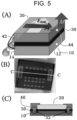
- FIG. 6 is a configuration perspective view illustrating an example of an application element to a thermoelectric power generation application or a heat flow sensor using the vertical thermoelectric conversion element of the present invention.
- thermopile structure As illustrated in FIG. 6 , a series voltage can be amplified by a simple in-plane connection type thermopile structure.
- thermoelectric layer a case where a Si substrate was stacked as a thermoelectric layer, a Co 2 MnGa thin film was stacked as a magnetic body layer, and a thermally oxidized SiO insulating film was stacked as an insulating layer is described, but the present invention is not limited thereto, and a thermoelectric material having a Seebeck effect can be used for the thermoelectric layer, a conductive ferromagnetic material can be used for the magnetic body layer, and an electrically insulating material having thermal conductivity can be used for the insulating layer.
- thermoelectric material having the Seebeck effect is selected from Bi 2 Te 3 , PbTe, Si, Ge, an FeSi alloy, a CrSi alloy, an MgSi alloy, a CoSb 3 alloy, an Fe 2 VAl-based Heusler's alloy, and SrTiO 3 .
- the vertical thermoelectric conversion element of the present invention can be used for a device with thermoelectric power generation application or a heat flow sensor.
Landscapes
- Chemical & Material Sciences (AREA)
- Inorganic Chemistry (AREA)
- Hall/Mr Elements (AREA)
Applications Claiming Priority (2)
| Application Number | Priority Date | Filing Date | Title |
|---|---|---|---|
| JP2020049595 | 2020-03-19 | ||
| PCT/JP2021/009982 WO2021187347A1 (ja) | 2020-03-19 | 2021-03-12 | 垂直型熱電変換素子、並びにこれを用いた熱電発電応用機器又は熱流センサー |
Publications (3)
| Publication Number | Publication Date |
|---|---|
| EP4123897A1 EP4123897A1 (en) | 2023-01-25 |
| EP4123897A4 EP4123897A4 (en) | 2024-05-15 |
| EP4123897B1 true EP4123897B1 (en) | 2024-12-11 |
Family
ID=77772110
Family Applications (1)
| Application Number | Title | Priority Date | Filing Date |
|---|---|---|---|
| EP21770787.6A Active EP4123897B1 (en) | 2020-03-19 | 2021-03-12 | Vertical thermoelectric conversion element and device with thermoelectric power generation application or heat flow sensor using same |
Country Status (4)
| Country | Link |
|---|---|
| US (1) | US11889762B2 (https=) |
| EP (1) | EP4123897B1 (https=) |
| JP (1) | JP7371980B2 (https=) |
| WO (1) | WO2021187347A1 (https=) |
Families Citing this family (7)
| Publication number | Priority date | Publication date | Assignee | Title |
|---|---|---|---|---|
| JP7669069B2 (ja) * | 2021-09-30 | 2025-04-28 | 国立研究開発法人物質・材料研究機構 | 熱電体、熱電発電素子、多層熱電体、多層熱電発電素子、熱電発電機、及び熱流センサ |
| JP7759024B2 (ja) * | 2021-11-30 | 2025-10-23 | 日産自動車株式会社 | 熱流束センサ、該熱流束センサを有する半導体装置、及び熱流束センサの製造方法 |
| JP7768606B2 (ja) * | 2022-05-16 | 2025-11-12 | 国立研究開発法人物質・材料研究機構 | 熱流センサ付きペルチェ素子 |
| JP2024087754A (ja) * | 2022-12-19 | 2024-07-01 | 国立大学法人 東京大学 | 非線形熱電効果測定装置、非線形熱電効果測定方法、非線形熱電効果測定プログラム、記録媒体、温度揺らぎ環境発電素子および温度揺らぎセンサー |
| CN115963437B (zh) * | 2022-12-21 | 2023-10-20 | 南方电网数字电网研究院有限公司 | 多量程磁传感器、磁场测量方法及导体制备方法 |
| WO2025047581A1 (ja) * | 2023-09-01 | 2025-03-06 | 国立研究開発法人物質・材料研究機構 | 熱電装置 |
| TR2024005002A2 (tr) * | 2024-04-26 | 2024-05-21 | Erguer Yusuf Furkan | Endüstri̇yel bacalardan atik isi geri̇ kazanimi i̇çi̇n bi̇r si̇stem |
Family Cites Families (11)
| Publication number | Priority date | Publication date | Assignee | Title |
|---|---|---|---|---|
| JP2001168403A (ja) * | 1999-12-13 | 2001-06-22 | Sumitomo Special Metals Co Ltd | 熱電変換素子 |
| JP2003060244A (ja) * | 2001-08-10 | 2003-02-28 | Sumitomo Special Metals Co Ltd | 冷却素子と熱電変換材料 |
| JP2008147304A (ja) * | 2006-12-07 | 2008-06-26 | Toyoda Gosei Co Ltd | 熱電変換素子 |
| JP5267967B2 (ja) | 2007-11-22 | 2013-08-21 | 国立大学法人東北大学 | スピン流熱変換素子及び熱電変換素子 |
| WO2010058464A1 (ja) * | 2008-11-20 | 2010-05-27 | 株式会社村田製作所 | 熱電変換モジュール |
| JP6079995B2 (ja) | 2012-09-28 | 2017-02-15 | 国立大学法人東北大学 | 熱電発電デバイス |
| WO2014147967A1 (ja) * | 2013-03-18 | 2014-09-25 | パナソニック株式会社 | テラヘルツ電磁波発生装置、テラヘルツ分光装置、およびテラヘルツ電磁波の発生方法 |
| JP6231467B2 (ja) * | 2014-11-27 | 2017-11-15 | トヨタ自動車株式会社 | 熱電体 |
| JPWO2018146713A1 (ja) * | 2017-02-07 | 2019-12-19 | 日本電気株式会社 | 熱電変換素子およびその製造方法 |
| WO2019009308A1 (ja) * | 2017-07-03 | 2019-01-10 | 国立大学法人東京大学 | 熱電変換素子及び熱電変換デバイス |
| JP7316579B2 (ja) * | 2018-12-18 | 2023-07-28 | 国立大学法人茨城大学 | 熱電変換装置 |
-
2021
- 2021-03-12 WO PCT/JP2021/009982 patent/WO2021187347A1/ja not_active Ceased
- 2021-03-12 JP JP2022508305A patent/JP7371980B2/ja active Active
- 2021-03-12 EP EP21770787.6A patent/EP4123897B1/en active Active
- 2021-03-12 US US17/801,061 patent/US11889762B2/en active Active
Also Published As
| Publication number | Publication date |
|---|---|
| EP4123897A1 (en) | 2023-01-25 |
| US20230102920A1 (en) | 2023-03-30 |
| EP4123897A4 (en) | 2024-05-15 |
| JP7371980B2 (ja) | 2023-10-31 |
| WO2021187347A1 (ja) | 2021-09-23 |
| US11889762B2 (en) | 2024-01-30 |
| JPWO2021187347A1 (https=) | 2021-09-23 |
Similar Documents
| Publication | Publication Date | Title |
|---|---|---|
| EP4123897B1 (en) | Vertical thermoelectric conversion element and device with thermoelectric power generation application or heat flow sensor using same | |
| JP5585314B2 (ja) | 熱電変換素子及び熱電変換装置 | |
| Uchida et al. | Thermoelectric generation based on spin Seebeck effects | |
| JP6079995B2 (ja) | 熱電発電デバイス | |
| JP5267967B2 (ja) | スピン流熱変換素子及び熱電変換素子 | |
| CN113728447A (zh) | 热电转换元件以及热电转换装置 | |
| Chen et al. | Topological Heusler Magnets‐Driven High‐Performance Transverse Nernst Thermoelectric Generators | |
| US20240284798A1 (en) | Thermoelectric body, thermoelectric generation element, multilayer thermoelectric body, multilayer thermoelectric generation element, thermoelectric generator, and heat flow sensor | |
| US20140224293A1 (en) | Thermoelectric conversion element | |
| Adachi et al. | Fundamentals and advances in transverse thermoelectrics | |
| US20180331273A1 (en) | Electromotive film for thermoelectric conversion element, and thermoelectric conversion element | |
| Shiomi et al. | Effect of scattering on intrinsic anomalous Hall effect investigated by Lorenz ratio | |
| JPWO2013035148A1 (ja) | 熱電変換素子及びそれを用いた熱電変換モジュール | |
| JP6565689B2 (ja) | 熱電変換素子、熱電変換素子モジュールおよび熱電変換素子の製造方法 | |
| US20240276881A1 (en) | Thermoelectric power generation device | |
| WO2025047008A1 (ja) | ハイブリッド横型熱電温度変調素子およびこれを用いた温度変調方法 | |
| JP7815834B2 (ja) | 熱電変換素子 | |
| Murata et al. | Measurements of Thermoelectric Properties of Identical Bi-Sb Sample in Magnetic Fields and Influence of Sample Geometry | |
| JPWO2025009336A5 (https=) | ||
| JP2003060244A (ja) | 冷却素子と熱電変換材料 | |
| JP7768606B2 (ja) | 熱流センサ付きペルチェ素子 | |
| WO2025009336A1 (ja) | 横熱電効果を用いた垂直型熱電変換素子、及び垂直型熱電変換素子の評価方法 | |
| Yamashita et al. | Effect of metal electrode on thermoelectric power in bismuth telluride compounds | |
| Fletcher | The Nernst-Ettinghausen coefficient and the Kondo effect in copper and gold | |
| WO2002017406A1 (fr) | Matiere de conversion thermoelectrique du groupe bi et element de conversion thermoelectrique |
Legal Events
| Date | Code | Title | Description |
|---|---|---|---|
| STAA | Information on the status of an ep patent application or granted ep patent |
Free format text: STATUS: THE INTERNATIONAL PUBLICATION HAS BEEN MADE |
|
| PUAI | Public reference made under article 153(3) epc to a published international application that has entered the european phase |
Free format text: ORIGINAL CODE: 0009012 |
|
| STAA | Information on the status of an ep patent application or granted ep patent |
Free format text: STATUS: REQUEST FOR EXAMINATION WAS MADE |
|
| 17P | Request for examination filed |
Effective date: 20220819 |
|
| AK | Designated contracting states |
Kind code of ref document: A1 Designated state(s): AL AT BE BG CH CY CZ DE DK EE ES FI FR GB GR HR HU IE IS IT LI LT LU LV MC MK MT NL NO PL PT RO RS SE SI SK SM TR |
|
| DAV | Request for validation of the european patent (deleted) | ||
| DAX | Request for extension of the european patent (deleted) | ||
| A4 | Supplementary search report drawn up and despatched |
Effective date: 20240412 |
|
| RIC1 | Information provided on ipc code assigned before grant |
Ipc: H10N 15/00 20230101ALI20240408BHEP Ipc: H10N 10/851 20230101ALI20240408BHEP Ipc: H10N 10/17 20230101ALI20240408BHEP Ipc: H02N 11/00 20060101AFI20240408BHEP |
|
| GRAP | Despatch of communication of intention to grant a patent |
Free format text: ORIGINAL CODE: EPIDOSNIGR1 |
|
| STAA | Information on the status of an ep patent application or granted ep patent |
Free format text: STATUS: GRANT OF PATENT IS INTENDED |
|
| INTG | Intention to grant announced |
Effective date: 20240923 |
|
| GRAS | Grant fee paid |
Free format text: ORIGINAL CODE: EPIDOSNIGR3 |
|
| GRAA | (expected) grant |
Free format text: ORIGINAL CODE: 0009210 |
|
| STAA | Information on the status of an ep patent application or granted ep patent |
Free format text: STATUS: THE PATENT HAS BEEN GRANTED |
|
| AK | Designated contracting states |
Kind code of ref document: B1 Designated state(s): AL AT BE BG CH CY CZ DE DK EE ES FI FR GB GR HR HU IE IS IT LI LT LU LV MC MK MT NL NO PL PT RO RS SE SI SK SM TR |
|
| REG | Reference to a national code |
Ref country code: GB Ref legal event code: FG4D |
|
| REG | Reference to a national code |
Ref country code: CH Ref legal event code: EP |
|
| REG | Reference to a national code |
Ref country code: DE Ref legal event code: R096 Ref document number: 602021023313 Country of ref document: DE |
|
| REG | Reference to a national code |
Ref country code: IE Ref legal event code: FG4D |
|
| REG | Reference to a national code |
Ref country code: LT Ref legal event code: MG9D |
|
| PG25 | Lapsed in a contracting state [announced via postgrant information from national office to epo] |
Ref country code: HR Free format text: LAPSE BECAUSE OF FAILURE TO SUBMIT A TRANSLATION OF THE DESCRIPTION OR TO PAY THE FEE WITHIN THE PRESCRIBED TIME-LIMIT Effective date: 20241211 |
|
| PG25 | Lapsed in a contracting state [announced via postgrant information from national office to epo] |
Ref country code: FI Free format text: LAPSE BECAUSE OF FAILURE TO SUBMIT A TRANSLATION OF THE DESCRIPTION OR TO PAY THE FEE WITHIN THE PRESCRIBED TIME-LIMIT Effective date: 20241211 |
|
| PG25 | Lapsed in a contracting state [announced via postgrant information from national office to epo] |
Ref country code: BG Free format text: LAPSE BECAUSE OF FAILURE TO SUBMIT A TRANSLATION OF THE DESCRIPTION OR TO PAY THE FEE WITHIN THE PRESCRIBED TIME-LIMIT Effective date: 20241211 |
|
| REG | Reference to a national code |
Ref country code: NL Ref legal event code: MP Effective date: 20241211 |
|
| PG25 | Lapsed in a contracting state [announced via postgrant information from national office to epo] |
Ref country code: ES Free format text: LAPSE BECAUSE OF FAILURE TO SUBMIT A TRANSLATION OF THE DESCRIPTION OR TO PAY THE FEE WITHIN THE PRESCRIBED TIME-LIMIT Effective date: 20241211 |
|
| PG25 | Lapsed in a contracting state [announced via postgrant information from national office to epo] |
Ref country code: NO Free format text: LAPSE BECAUSE OF FAILURE TO SUBMIT A TRANSLATION OF THE DESCRIPTION OR TO PAY THE FEE WITHIN THE PRESCRIBED TIME-LIMIT Effective date: 20250311 |
|
| PG25 | Lapsed in a contracting state [announced via postgrant information from national office to epo] |
Ref country code: GR Free format text: LAPSE BECAUSE OF FAILURE TO SUBMIT A TRANSLATION OF THE DESCRIPTION OR TO PAY THE FEE WITHIN THE PRESCRIBED TIME-LIMIT Effective date: 20250312 Ref country code: LV Free format text: LAPSE BECAUSE OF FAILURE TO SUBMIT A TRANSLATION OF THE DESCRIPTION OR TO PAY THE FEE WITHIN THE PRESCRIBED TIME-LIMIT Effective date: 20241211 |
|
| PG25 | Lapsed in a contracting state [announced via postgrant information from national office to epo] |
Ref country code: RS Free format text: LAPSE BECAUSE OF FAILURE TO SUBMIT A TRANSLATION OF THE DESCRIPTION OR TO PAY THE FEE WITHIN THE PRESCRIBED TIME-LIMIT Effective date: 20250311 |
|
| PG25 | Lapsed in a contracting state [announced via postgrant information from national office to epo] |
Ref country code: NL Free format text: LAPSE BECAUSE OF FAILURE TO SUBMIT A TRANSLATION OF THE DESCRIPTION OR TO PAY THE FEE WITHIN THE PRESCRIBED TIME-LIMIT Effective date: 20241211 |
|
| REG | Reference to a national code |
Ref country code: AT Ref legal event code: MK05 Ref document number: 1751161 Country of ref document: AT Kind code of ref document: T Effective date: 20241211 |
|
| PG25 | Lapsed in a contracting state [announced via postgrant information from national office to epo] |
Ref country code: SM Free format text: LAPSE BECAUSE OF FAILURE TO SUBMIT A TRANSLATION OF THE DESCRIPTION OR TO PAY THE FEE WITHIN THE PRESCRIBED TIME-LIMIT Effective date: 20241211 |
|
| PG25 | Lapsed in a contracting state [announced via postgrant information from national office to epo] |
Ref country code: PL Free format text: LAPSE BECAUSE OF FAILURE TO SUBMIT A TRANSLATION OF THE DESCRIPTION OR TO PAY THE FEE WITHIN THE PRESCRIBED TIME-LIMIT Effective date: 20241211 |
|
| PG25 | Lapsed in a contracting state [announced via postgrant information from national office to epo] |
Ref country code: IS Free format text: LAPSE BECAUSE OF FAILURE TO SUBMIT A TRANSLATION OF THE DESCRIPTION OR TO PAY THE FEE WITHIN THE PRESCRIBED TIME-LIMIT Effective date: 20250411 |
|
| PG25 | Lapsed in a contracting state [announced via postgrant information from national office to epo] |
Ref country code: PT Free format text: LAPSE BECAUSE OF FAILURE TO SUBMIT A TRANSLATION OF THE DESCRIPTION OR TO PAY THE FEE WITHIN THE PRESCRIBED TIME-LIMIT Effective date: 20250411 |
|
| PG25 | Lapsed in a contracting state [announced via postgrant information from national office to epo] |
Ref country code: EE Free format text: LAPSE BECAUSE OF FAILURE TO SUBMIT A TRANSLATION OF THE DESCRIPTION OR TO PAY THE FEE WITHIN THE PRESCRIBED TIME-LIMIT Effective date: 20241211 |
|
| PG25 | Lapsed in a contracting state [announced via postgrant information from national office to epo] |
Ref country code: AT Free format text: LAPSE BECAUSE OF FAILURE TO SUBMIT A TRANSLATION OF THE DESCRIPTION OR TO PAY THE FEE WITHIN THE PRESCRIBED TIME-LIMIT Effective date: 20241211 Ref country code: RO Free format text: LAPSE BECAUSE OF FAILURE TO SUBMIT A TRANSLATION OF THE DESCRIPTION OR TO PAY THE FEE WITHIN THE PRESCRIBED TIME-LIMIT Effective date: 20241211 |
|
| PG25 | Lapsed in a contracting state [announced via postgrant information from national office to epo] |
Ref country code: SK Free format text: LAPSE BECAUSE OF FAILURE TO SUBMIT A TRANSLATION OF THE DESCRIPTION OR TO PAY THE FEE WITHIN THE PRESCRIBED TIME-LIMIT Effective date: 20241211 |
|
| PG25 | Lapsed in a contracting state [announced via postgrant information from national office to epo] |
Ref country code: CZ Free format text: LAPSE BECAUSE OF FAILURE TO SUBMIT A TRANSLATION OF THE DESCRIPTION OR TO PAY THE FEE WITHIN THE PRESCRIBED TIME-LIMIT Effective date: 20241211 |
|
| PG25 | Lapsed in a contracting state [announced via postgrant information from national office to epo] |
Ref country code: IT Free format text: LAPSE BECAUSE OF FAILURE TO SUBMIT A TRANSLATION OF THE DESCRIPTION OR TO PAY THE FEE WITHIN THE PRESCRIBED TIME-LIMIT Effective date: 20241211 |
|
| PG25 | Lapsed in a contracting state [announced via postgrant information from national office to epo] |
Ref country code: SE Free format text: LAPSE BECAUSE OF FAILURE TO SUBMIT A TRANSLATION OF THE DESCRIPTION OR TO PAY THE FEE WITHIN THE PRESCRIBED TIME-LIMIT Effective date: 20241211 |
|
| REG | Reference to a national code |
Ref country code: DE Ref legal event code: R097 Ref document number: 602021023313 Country of ref document: DE |
|
| PG25 | Lapsed in a contracting state [announced via postgrant information from national office to epo] |
Ref country code: DK Free format text: LAPSE BECAUSE OF FAILURE TO SUBMIT A TRANSLATION OF THE DESCRIPTION OR TO PAY THE FEE WITHIN THE PRESCRIBED TIME-LIMIT Effective date: 20241211 |
|
| PG25 | Lapsed in a contracting state [announced via postgrant information from national office to epo] |
Ref country code: MC Free format text: LAPSE BECAUSE OF FAILURE TO SUBMIT A TRANSLATION OF THE DESCRIPTION OR TO PAY THE FEE WITHIN THE PRESCRIBED TIME-LIMIT Effective date: 20241211 |
|
| PLBE | No opposition filed within time limit |
Free format text: ORIGINAL CODE: 0009261 |
|
| STAA | Information on the status of an ep patent application or granted ep patent |
Free format text: STATUS: NO OPPOSITION FILED WITHIN TIME LIMIT |
|
| REG | Reference to a national code |
Ref country code: CH Ref legal event code: L10 Free format text: ST27 STATUS EVENT CODE: U-0-0-L10-L00 (AS PROVIDED BY THE NATIONAL OFFICE) Effective date: 20251022 |
|
| REG | Reference to a national code |
Ref country code: CH Ref legal event code: H13 Free format text: ST27 STATUS EVENT CODE: U-0-0-H10-H13 (AS PROVIDED BY THE NATIONAL OFFICE) Effective date: 20251023 |
|
| PG25 | Lapsed in a contracting state [announced via postgrant information from national office to epo] |
Ref country code: LU Free format text: LAPSE BECAUSE OF NON-PAYMENT OF DUE FEES Effective date: 20250312 |
|
| 26N | No opposition filed |
Effective date: 20250912 |
|
| GBPC | Gb: european patent ceased through non-payment of renewal fee |
Effective date: 20250312 |
|
| REG | Reference to a national code |
Ref country code: BE Ref legal event code: MM Effective date: 20250331 |
|
| PG25 | Lapsed in a contracting state [announced via postgrant information from national office to epo] |
Ref country code: GB Free format text: LAPSE BECAUSE OF NON-PAYMENT OF DUE FEES Effective date: 20250312 |
|
| PG25 | Lapsed in a contracting state [announced via postgrant information from national office to epo] |
Ref country code: FR Free format text: LAPSE BECAUSE OF NON-PAYMENT OF DUE FEES Effective date: 20250331 |
|
| PG25 | Lapsed in a contracting state [announced via postgrant information from national office to epo] |
Ref country code: BE Free format text: LAPSE BECAUSE OF NON-PAYMENT OF DUE FEES Effective date: 20250331 |
|
| PG25 | Lapsed in a contracting state [announced via postgrant information from national office to epo] |
Ref country code: CH Free format text: LAPSE BECAUSE OF NON-PAYMENT OF DUE FEES Effective date: 20250331 |
|
| PG25 | Lapsed in a contracting state [announced via postgrant information from national office to epo] |
Ref country code: IE Free format text: LAPSE BECAUSE OF NON-PAYMENT OF DUE FEES Effective date: 20250312 |
|
| PGFP | Annual fee paid to national office [announced via postgrant information from national office to epo] |
Ref country code: DE Payment date: 20260114 Year of fee payment: 6 |