EP4120366A1 - Rückseitenkontaktierter solarzellenstrang und herstellungsverfahren dafür - Google Patents
Rückseitenkontaktierter solarzellenstrang und herstellungsverfahren dafür Download PDFInfo
- Publication number
- EP4120366A1 EP4120366A1 EP21000332.3A EP21000332A EP4120366A1 EP 4120366 A1 EP4120366 A1 EP 4120366A1 EP 21000332 A EP21000332 A EP 21000332A EP 4120366 A1 EP4120366 A1 EP 4120366A1
- Authority
- EP
- European Patent Office
- Prior art keywords
- electrode regions
- positive electrode
- negative electrode
- insulation layers
- bus bar
- Prior art date
- Legal status (The legal status is an assumption and is not a legal conclusion. Google has not performed a legal analysis and makes no representation as to the accuracy of the status listed.)
- Pending
Links
Images


Classifications
-
- H—ELECTRICITY
- H10—SEMICONDUCTOR DEVICES; ELECTRIC SOLID-STATE DEVICES NOT OTHERWISE PROVIDED FOR
- H10F—INORGANIC SEMICONDUCTOR DEVICES SENSITIVE TO INFRARED RADIATION, LIGHT, ELECTROMAGNETIC RADIATION OF SHORTER WAVELENGTH OR CORPUSCULAR RADIATION
- H10F77/00—Constructional details of devices covered by this subclass
- H10F77/93—Interconnections
- H10F77/933—Interconnections for devices having potential barriers
- H10F77/935—Interconnections for devices having potential barriers for photovoltaic devices or modules
- H10F77/937—Busbar structures for modules
-
- H—ELECTRICITY
- H10—SEMICONDUCTOR DEVICES; ELECTRIC SOLID-STATE DEVICES NOT OTHERWISE PROVIDED FOR
- H10F—INORGANIC SEMICONDUCTOR DEVICES SENSITIVE TO INFRARED RADIATION, LIGHT, ELECTROMAGNETIC RADIATION OF SHORTER WAVELENGTH OR CORPUSCULAR RADIATION
- H10F10/00—Individual photovoltaic cells, e.g. solar cells
- H10F10/10—Individual photovoltaic cells, e.g. solar cells having potential barriers
- H10F10/14—Photovoltaic cells having only PN homojunction potential barriers
- H10F10/146—Back-junction photovoltaic cells, e.g. having interdigitated base-emitter regions on the back side
-
- H—ELECTRICITY
- H10—SEMICONDUCTOR DEVICES; ELECTRIC SOLID-STATE DEVICES NOT OTHERWISE PROVIDED FOR
- H10F—INORGANIC SEMICONDUCTOR DEVICES SENSITIVE TO INFRARED RADIATION, LIGHT, ELECTROMAGNETIC RADIATION OF SHORTER WAVELENGTH OR CORPUSCULAR RADIATION
- H10F19/00—Integrated devices, or assemblies of multiple devices, comprising at least one photovoltaic cell covered by group H10F10/00, e.g. photovoltaic modules
- H10F19/90—Structures for connecting between photovoltaic cells, e.g. interconnections or insulating spacers
- H10F19/902—Structures for connecting between photovoltaic cells, e.g. interconnections or insulating spacers for series or parallel connection of photovoltaic cells
- H10F19/908—Structures for connecting between photovoltaic cells, e.g. interconnections or insulating spacers for series or parallel connection of photovoltaic cells for back-contact photovoltaic cells
-
- H—ELECTRICITY
- H10—SEMICONDUCTOR DEVICES; ELECTRIC SOLID-STATE DEVICES NOT OTHERWISE PROVIDED FOR
- H10F—INORGANIC SEMICONDUCTOR DEVICES SENSITIVE TO INFRARED RADIATION, LIGHT, ELECTROMAGNETIC RADIATION OF SHORTER WAVELENGTH OR CORPUSCULAR RADIATION
- H10F71/00—Manufacture or treatment of devices covered by this subclass
-
- H—ELECTRICITY
- H10—SEMICONDUCTOR DEVICES; ELECTRIC SOLID-STATE DEVICES NOT OTHERWISE PROVIDED FOR
- H10F—INORGANIC SEMICONDUCTOR DEVICES SENSITIVE TO INFRARED RADIATION, LIGHT, ELECTROMAGNETIC RADIATION OF SHORTER WAVELENGTH OR CORPUSCULAR RADIATION
- H10F77/00—Constructional details of devices covered by this subclass
- H10F77/20—Electrodes
- H10F77/206—Electrodes for devices having potential barriers
- H10F77/211—Electrodes for devices having potential barriers for photovoltaic cells
- H10F77/219—Arrangements for electrodes of back-contact photovoltaic cells
-
- H—ELECTRICITY
- H10—SEMICONDUCTOR DEVICES; ELECTRIC SOLID-STATE DEVICES NOT OTHERWISE PROVIDED FOR
- H10F—INORGANIC SEMICONDUCTOR DEVICES SENSITIVE TO INFRARED RADIATION, LIGHT, ELECTROMAGNETIC RADIATION OF SHORTER WAVELENGTH OR CORPUSCULAR RADIATION
- H10F77/00—Constructional details of devices covered by this subclass
- H10F77/30—Coatings
- H10F77/306—Coatings for devices having potential barriers
- H10F77/311—Coatings for devices having potential barriers for photovoltaic cells
-
- H—ELECTRICITY
- H10—SEMICONDUCTOR DEVICES; ELECTRIC SOLID-STATE DEVICES NOT OTHERWISE PROVIDED FOR
- H10F—INORGANIC SEMICONDUCTOR DEVICES SENSITIVE TO INFRARED RADIATION, LIGHT, ELECTROMAGNETIC RADIATION OF SHORTER WAVELENGTH OR CORPUSCULAR RADIATION
- H10F77/00—Constructional details of devices covered by this subclass
- H10F77/40—Optical elements or arrangements
- H10F77/42—Optical elements or arrangements directly associated or integrated with photovoltaic cells, e.g. light-reflecting means or light-concentrating means
- H10F77/488—Reflecting light-concentrating means, e.g. parabolic mirrors or concentrators using total internal reflection
-
- H—ELECTRICITY
- H10—SEMICONDUCTOR DEVICES; ELECTRIC SOLID-STATE DEVICES NOT OTHERWISE PROVIDED FOR
- H10F—INORGANIC SEMICONDUCTOR DEVICES SENSITIVE TO INFRARED RADIATION, LIGHT, ELECTROMAGNETIC RADIATION OF SHORTER WAVELENGTH OR CORPUSCULAR RADIATION
- H10F77/00—Constructional details of devices covered by this subclass
- H10F77/70—Surface textures, e.g. pyramid structures
- H10F77/703—Surface textures, e.g. pyramid structures of the semiconductor bodies, e.g. textured active layers
-
- Y—GENERAL TAGGING OF NEW TECHNOLOGICAL DEVELOPMENTS; GENERAL TAGGING OF CROSS-SECTIONAL TECHNOLOGIES SPANNING OVER SEVERAL SECTIONS OF THE IPC; TECHNICAL SUBJECTS COVERED BY FORMER USPC CROSS-REFERENCE ART COLLECTIONS [XRACs] AND DIGESTS
- Y02—TECHNOLOGIES OR APPLICATIONS FOR MITIGATION OR ADAPTATION AGAINST CLIMATE CHANGE
- Y02E—REDUCTION OF GREENHOUSE GAS [GHG] EMISSIONS, RELATED TO ENERGY GENERATION, TRANSMISSION OR DISTRIBUTION
- Y02E10/00—Energy generation through renewable energy sources
- Y02E10/50—Photovoltaic [PV] energy
- Y02E10/52—PV systems with concentrators
-
- Y—GENERAL TAGGING OF NEW TECHNOLOGICAL DEVELOPMENTS; GENERAL TAGGING OF CROSS-SECTIONAL TECHNOLOGIES SPANNING OVER SEVERAL SECTIONS OF THE IPC; TECHNICAL SUBJECTS COVERED BY FORMER USPC CROSS-REFERENCE ART COLLECTIONS [XRACs] AND DIGESTS
- Y02—TECHNOLOGIES OR APPLICATIONS FOR MITIGATION OR ADAPTATION AGAINST CLIMATE CHANGE
- Y02E—REDUCTION OF GREENHOUSE GAS [GHG] EMISSIONS, RELATED TO ENERGY GENERATION, TRANSMISSION OR DISTRIBUTION
- Y02E10/00—Energy generation through renewable energy sources
- Y02E10/50—Photovoltaic [PV] energy
- Y02E10/547—Monocrystalline silicon PV cells
Definitions
- the disclosure relates to the field of solar cells, and in particular, to a back contact solar cell string and a preparation method therefor, a module, and a system.
- a solar cell is a semiconductor device capable of converting light energy to electric energy.
- the solar cell industry pursues low production costs and high energy conversion efficiency.
- an emitter contact electrode and a base contact electrode thereof are respectively located on two opposite sides of a cell piece.
- the front side of the cell is a light-receiving surface.
- the front metal electrode of a common crystalline silicon solar cell is covered by about 7% in area.
- the energy conversion efficiency of the cell may be directly enhanced by reducing the covering of the front metal electrode.
- a back contact solar cell is a cell in which contact electrodes of emitter and base are both disposed on a back side (a non-light-receiving surface) of the cell.
- the front surface without metal electrode of back contact cells increases the light-receiving area, effectively increasing the short-circuit current of a cell piece.
- a relatively wide metal grid line is allowed to exist on the back side of back contact cells to reduce the serial resistance, thereby increasing the fill factors.
- the cell without front shielding not only has high conversion efficiency, but also has a more pleasing appearance.
- a module having electrodes all disposed on a back side is easy to assemble.
- the technical problem to be resolved in the disclosure is to provide a back contact solar cell string, to resolve the problems such as the requirement for accurate cell alignment and the complexity of the process during the manufacturing of a conventional cell string.
- the back contact solar cell string comprises:
- solder joints are disposed in the positive electrode regions and the negative electrode regions on the cell pieces that are electrically connected to the first bus bar.
- conductive adhesives or solder pastes are disposed at connection portions between the first bus bar and the positive electrode regions and the negative electrode regions on the cell pieces.
- the conductive adhesives or the solder pastes are disposed on the first bus bar.
- the first bus bar comprises a main body portion and extending portions each extending from the main body portion and connected to the positive electrode regions and the negative electrode regions.
- a reflection structure is disposed on the main body portion.
- the reflection structure is a roughly textured structure, a reflective layer coated on the main body portion, or a reflective film attached to the main body portion.
- the reflective film is an aluminum film.
- the reflection structure is located in a gap between the two adjacent cell pieces.
- the insulation layers comprise insulation pastes.
- the first bus bar is a pressure-sensitive conductive adhesive tape or a ribbon.
- the cell string further comprises second bus bars located on end portions of the solar cell string, and the second bus bars are electrically connected to the positive electrode regions and the negative electrode regions in the cell pieces located on the end portions that are not covered by the insulation layers.
- a quantity of the solder joints is in a range of 2-20.
- the disclosure further provides a cell module.
- the cell module comprises the back contact solar cell string described above.
- the disclosure further provides a photovoltaic system.
- the photovoltaic system comprises the cell module described above.
- the disclosure further provides a method for preparing a back contact solar cell string.
- the method comprises:
- connecting the first bus bar to the positive electrode regions and the negative electrode regions in the two adjacent cell pieces that are not covered by the insulation layers comprises:
- connecting the first bus bar to the positive electrode regions and the negative electrode regions in the two adjacent cell pieces that are not covered by the insulation layers comprises:
- connecting the first bus bar to the positive electrode regions and the negative electrode regions in the two adjacent cell pieces that are not covered by the insulation layers comprises:
- the method further comprises: connecting second bus bars to the positive electrode regions or the negative electrode regions in the cell pieces located on end portions that are not covered by the insulation layers.
- the positive electrode regions and the negative electrode regions on the cell pieces that are not required to be electrically connected are covered by using the insulation layers, and the first bus bars can be directly connected to all of the positive electrode regions and the negative electrode regions on the cell pieces.
- the insulation layers are disposed, so that the positive electrode regions and the negative electrode regions not required to be electrically connected are insulated from the first bus bars by using the insulation layers, and the positive electrode regions and the negative electrode regions required to be electrically connected are directly electrically connected to the first bus bars.
- the reflection structures are disposed on the first bus bars, so that light can be reflected back to glass in a manufactured cell module, and then reflected to an adjacent cell piece through the glass, and the adjacent cell piece can absorb the light irradiated on the first bus bars. In this way, secondary reflection and utilization of the light irradiated on the cell module can be increased, thereby enhancing the power.
- connection may be a fixed connection, a detachable connection, or an integral connection; or the connection may be a mechanical connection or an electrical connection; or the connection may be a direct connection, an indirect connection through an intermediary, or internal communication between two components.
- positive electrode regions and negative electrode regions on cell pieces that are not required to be electrically connected are covered by using insulation layers, and first bus bars can be directly connected to all of the positive electrode regions and the negative electrode regions on the cell pieces.
- the insulation layers are disposed, so that the positive electrode regions and the negative electrode regions not required to be electrically connected are insulated from the first bus bars by using the insulation layers, and the positive electrode regions and the negative electrode regions required to be electrically connected are directly electrically connected to the first bus bars.
- the reflection structures are disposed on the first bus bars, so that light can be reflected back to glass in a manufactured cell module, and then reflected to an adjacent cell piece through the glass, and the adjacent cell piece can absorb the light irradiated on the first bus bars. In this way, secondary reflection and utilization of the light irradiated on the cell module can be increased, thereby enhancing the power.
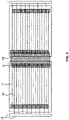
- FIG. 1 is a schematic structural diagram of a back contact solar cell string according to an embodiment of the disclosure. For ease of description, only parts related to this embodiment of the disclosure are shown.
- the back contact solar cell string provided in this embodiment of the disclosure comprises:
- the back contact solar cell string is a cell string formed by serially connecting at least two cell pieces (that is, back contact solar cells) together using the first bus bar 14 disposed between each two cell pieces.
- the cell string may comprise two cell pieces, three cell pieces, or other quantities of cell pieces that are serially connected to each other.
- FIG. 1 , FIG. 3 , FIG. 4 , and FIG. 5 show a cell string formed by two cell pieces serially connected to each other. In this case, only one first bus bar 14 is required to be connected to the two adjacent cell pieces.
- FIG. 2 shows a cell string comprising three cell pieces serially connected to each other. In this case, two first bus bar 14 are required to be respectively connected to the two adjacent cell pieces.
- the cell string may also comprise other quantities of cell pieces serially connected to each other according to actual use requirements, which is not completely shown in the figure.
- the cell string is designed according to actual requirements.
- the cell pieces at two end portions of the cell string are defined as end cell pieces.
- the cell pieces serially connected between the two end cell pieces are defined as internal cell pieces.
- the cell pieces each comprise a front passivation and anti-reflection layer, a silicon substrate, a back tunneling layer, N-type doped regions and P-type doped regions alternately disposed, a back passivation layer, and a cell electrode from top to bottom.
- the N-type doped regions and the P-type doped regions are alternately disposed on a lower surface of the back tunneling layer.
- the cell electrode comprises positive electrode thin grid lines and negative electrode thin grid lines.
- the positive electrode thin grid lines are electrically connected to the P-type doped region to form the positive electrode regions 11.
- the negative electrode thin grid lines are electrically connected to the N-type doped region to form the negative electrode regions 12.
- a structure of the cell piece may also be designed differently, which is not limited herein.
- the positive electrode thin grid lines are disposed in the P-type doped region to form the positive electrode regions 11
- the negative electrode thin grid lines are disposed in the N-type doped region to form the negative electrode regions 12
- the positive electrode regions 11 and the negative electrode regions 12 are all disposed on a back side of the cell piece.
- the positive electrode thin grid lines and the negative electrode thin grid lines may extend to end portions of the cell piece. Altematively, a specific distance may be designed between ends of the positive electrode thin grid lines and the negative electrode thin grid lines and the end portions of the cell piece.
- FIG. 1 is a back view of the cell string.
- the cell string comprises a plurality of positive electrode regions 11 and negative electrode regions 12 that are alternately disposed. All of the positive electrode regions 11 and the negative electrode regions 12 are substantially parallel to an edge of the cell piece and are alternately disposed.
- the cell pieces are substantially in rectangular shapes.
- the expression "the cell pieces are substantially rectangular cell pieces” means that, for example, the cell pieces may be in square shapes, or may be in another rectangular shape, and may have standard corners, cut corners, or rounded corner.
- the cell pieces are designed according to actual production requirements, which are not specifically limited herein. Quantities of the positive electrode regions 11 and the negative electrode regions 12 are determined according to actual sizes of the cell pieces and widths of the positive electrode thin grid lines and the negative electrode thin grid lines and distances therebetween, which are not specifically limited herein.
- the positive electrode regions 11 on one side of each cell piece are covered by the insulation layers 13, and the negative electrode regions 12 on another side of each cell piece are also covered by the insulation layers 13.
- the insulation layers 13 may be insulation pastes, or may be non-conductive adhesive tapes or insulation films, or may be other proper non-conductive shields or covers.
- the insulation layers 13 may comprise materials such as polypropylene, polyethylene, or polyimide, and may further comprise acrylic bonding layers.
- the insulation layers 13 may be in circular shapes, square shapes, triangular shapes, or other shapes.
- the shapes and materials of the insulation layers 13 may be designed according to actual use requirements, provided that the insulation layers can realize insulation between the positive electrode regions 11 or the negative electrode regions 12 that are covered and the outside, which are not specifically limited herein.
- the insulation layers 13 may be preferably spread outward by using ends of the positive electrode regions 11 or the negative electrode regions 12 that are required to be covered as centers.
- the insulation layers 13 may be coated from the ends of the positive electrode regions 11 to the end portions of the cell pieces.
- one region (the positive electrode region 11 or the negative electrode region 12) on one side of the cell piece is covered by the insulation layers 13, and another region is not covered by the insulation layers 13, so that the region not covered by the insulation layers 13 may be connected to the outside, and the region covered by the insulation layers 13 may be insulated from the outside.
- connection is established from a polarity of a cell piece to another polarity of a next adjacent cell piece by using the first bus bar 14, to achieve the connection between the cell pieces.
- the first bus bar 14 is electrically connected to the positive electrode regions 11 and the negative electrode regions 12 in the two adjacent cell pieces that are not covered by the insulation layers 13. That is to say, for example, on the two cell pieces, the positive electrode regions 11 on a left side are covered by the insulation layers 13 and the negative electrode regions 12 on a right side are covered by the insulation layers 13.
- the negative electrode regions 12 are insulated from the first bus bar 14 by means of the insulation layers 13 disposed on the right side of the end cell piece on a left side, and the positive electrode regions 11 not covered by the insulation layers 13 are electrically connected to the first bus bar 14.
- the positive electrode regions 11 are insulated from the first bus bar 14 by means of the insulation layers 13 disposed on the left side of the end cell piece on a right side, and the negative electrode regions 12 not covered by the insulation layers 13 are electrically connected to the first bus bar 14.
- the positive electrode regions 11 of the end cell piece on the left side are connected to the negative electrode regions 12 of the adjacent end cell piece on the right side by using the first bus bar 14.
- a connection range of the connection between the first bus bar 14 and the two adjacent cell pieces does not exceed a coverage of the insulation layers 13, so that the first bus bar 14 is insulated from the positive electrode regions 11 or the negative electrode regions 12 that are covered by the insulation layers 13.
- a current in the negative electrode regions 12 of the end cell piece on the left side flows from inside of the cell piece to the adjacent positive electrode regions 11.
- the positive electrode regions 11 are electrically connected to the first bus bar 14, so that a current in the positive electrode regions 11 of the end cell piece on the left side flows to the negative electrode regions 12 of the end cell piece on the right side by using the first bus bar 14, and further flows from the inside of the end cell piece on the right side to the adjacent positive electrode regions 11.
- the serial connection between cell pieces is realized. It is to be understood that, when there are 3 or other quantities of cell pieces, the cell pieces are correspondingly electrically connected to each other by using the first bus bars 14.
- the first bus bars 14 are respectively connected to the positive electrode regions 11 and the negative electrode regions 12 in the respective two adjacent cell pieces that are not covered by the insulation layers 13. Left sides of all of the first bus bars 14 are all electrically connected to the positive electrode regions 11, and right sides of the first bus bars are all electrically connected to the negative electrode regions 12. Therefore, the serial connection between cell pieces is realized. In this way, the current may flow from one cell piece to the next adjacent cell piece by using the first bus bars 14, and is finally exported.
- the positive electrode regions 11 and the negative electrode regions 12 on each cell piece that are not covered by the insulation layers 13 may be directly electrically connected to the first bus bar 14.
- Conductive adhesives or solder pastes 15 are disposed at connection portions between the first bus bar 14 and the positive electrode regions 11 and the negative electrode regions 12 on the cell piece.
- the conductive adhesives or the solder pastes 15 are directly coated in the positive electrode regions 11 and the negative electrode regions 12 on the cell piece that are not covered by the insulation layers 13.
- the first bus bar 14 can directly come into contact with the conductive adhesives or the solder pastes 15 during connection to the cell piece, so that more desirable electrical connection and physical connection with the positive electrode regions 11 and the negative electrode regions 12 that are required to be connected are realized.
- the conductive adhesives or the solder pastes 15 are required to be successively disposed in each positive electrode region 11 and each negative electrode region 12 that are not covered by the insulation layers 13, which is relatively cumbersome.
- the conductive adhesives or the solder pastes 15 are required to be coated accurately enough. As shown in FIG.
- the conductive adhesives or the solder pastes 15 are coated on the first bus bar 14, that is, the conductive adhesives or the solder pastes 15 are disposed on the first bus bar 14.
- the conductive adhesives or the solder pastes 15 disposed on the first bus bar 14 are merely required to be controlled not to exceed the coverage of the insulation layers 13.
- the conductive adhesives or the solder pastes 15 may be directly completely and continuously disposed on a periphery of the first bus bar 14.
- the first bus bar 14 can be electrically connected to each positive electrode region 11 and each negative electrode region 12 that are not covered by the insulation layers 13 more desirably by using the conductive adhesives or the solder pastes 15.
- the first bus bar is still prevented from being electrically connected to the negative electrode regions 12 or the positive electrode regions 11 that are covered by the insulation layers 13.
- the negative electrode regions 12 or the positive electrode regions 11 that are covered by the insulation layers 13 are successively covered by the insulation layers 13, the conductive adhesives or the solder pastes 15, and the first bus bar 14. Therefore, coating the conductive adhesives or the solder pastes 15 on the first bus bar 14 is a convenient and rapid process operation.
- busbars or wires 16 connected to each positive electrode region 11 or each negative electrode region 12 that is not covered by the insulation layers 13 are further disposed on each cell piece.
- the negative electrode regions 12 not covered by the insulation layers 13 may be connected to the busbars or the wires 16.
- the first bus bar 14 is electrically connected to the positive electrode regions 11 and the negative electrode regions 12 in the two adjacent cell pieces that are not covered by the insulation layers 13 mainly by using the busbars or the wires 16.
- each positive electrode region 11 or each negative electrode region 12 that is covered by the insulation layers 13 is prevented from being connected to the first bus bar 14.
- the conductive adhesives or the solder pastes 15 are disposed on the connection portions between the first bus bar 14 and the positive electrode regions 11 and the negative electrode regions 12 on the cell pieces.
- the conductive adhesives or the solder pastes 15 may be coated on the busbars or the wires 16.
- the conductive adhesives or the solder pastes 15 may be directly coated on the first bus bar 14. Further, in an embodiment of the disclosure, as shown in FIG.
- the positive electrode regions 11 having a same polarity may all be disposed close to one side, and the negative electrode regions 12 are all disposed close to an other side.
- the positive electrode regions 11 on the left side on the cell piece are coated with the insulation layers 13, and the negative electrode regions 12 on the right side are coated with the insulation layers 13.
- the negative electrode regions 12 are disposed close to the left side, and the positive electrode regions 11 are disposed close to the right side. Therefore, the negative electrode regions 12 on the left side may be caused to protrude out of the positive electrode regions 11 coated with the insulation layers 13, so that the negative electrode regions 12 on the left side do not come into contact with the positive electrode regions 11 during connection to the busbars or the wires 16.
- the positive electrode regions 11 not only realizes insulation from the outside by using the insulation layers 13 covered thereon, but also do not come into contact with the busbars or the wires 16 by means of an offset position.
- the positive electrode regions 11 and the negative electrode regions 12 are all regularly and alternately disposed on a back side of the cell piece. In this case, the insulation layers 13 are required to be coated first, and then the busbars or the wires 16 are disposed.
- solder joints 17 may be further disposed on the busbars or the wires 16. That is to say, the solder joints 17 are disposed in the positive electrode regions 11 and the negative electrode regions 12 of the cell piece that are electrically connected to the first bus bar 14. A plurality of solder joints 17 are disposed on the busbars or the wires 16, so as to achieve more desirable electrical connection and physical connection to the first bus bar 14 by using the solder joints 17. A quantity of the solder joints 17 is in a range of 2-20.
- the solder joints 17 may be disposed in part of the positive electrode regions 11 or the negative electrode regions 12.
- the rest of the positive electrode regions 11 or the negative electrode regions 12 are directly connected to the busbars or the wires 16.
- the first bus bar 14 is electrically connected to the positive electrode regions 11 and the negative electrode regions 12 in the two adjacent cell pieces that are not covered by the insulation layers 13 respectively by using the solder joints 17 and the busbars or the wires 16.
- the conductive adhesives or the solder pastes 15 are disposed on the connection portions between the first bus bar 14 and the positive electrode regions 11 and the negative electrode regions 12 on the cell pieces. Specifically, the conductive adhesives or the solder pastes 15 may be coated on the solder joints 17. Alternatively, the conductive adhesives or the solder pastes 15 may be directly coated on the first bus bar 14.
- the first bus bar 14 is a pressure-sensitive conductive adhesive tape or a ribbon.
- the first bus bar 14 comprises a main body portion 141 and extending portions 142 each extending from the main body portion 141 and connected to the positive electrode regions 11 and the negative electrode regions 12.
- the extending portions 142 extend from the main body portion 141 to form a finger-like shape or a comb-like shape.
- solder joints 17 are alternately disposed, so that the solder joints 17 disposed in the positive electrode regions 11 in a cell piece that are required to be electrically connected correspond to the solder joints 17 disposed in the negative electrode regions 12 in an adjacent cell piece that are required to be electrically connected, thereby achieving corresponding connection between the first bus bar 14 and the solder joints 17.
- each extending portion 142 is connected to only each positive electrode region 11 or each negative electrode region 12 on the cell piece that is not covered by the insulation layers 13, and is not connected to each adjacent negative electrode region 12 or each adjacent positive electrode region 11 that is covered by the insulation layers 13, physical disconnection between the first bus bar 14 and the negative electrode regions 12 or the positive electrode regions 11 that are covered by the insulation layers 13 can be realized on the basis of the insulation layers 13. In this way, the short circuit caused by the connection between the negative electrode regions 12 or the positive electrode regions 11 that are not completely covered by the insulation layers 13 and the first bus bar 14 is avoided.
- the extending portions may also extend to be fused into a whole.
- the first bus bar 14 may comprise the main body portion and two extending portions extending from two ends of the main body portion.
- the extending portions are connected to the corresponding positive electrode regions 11 or negative electrode regions 12 that are not covered by the insulation layers.
- the positive electrode regions 11 or the negative electrode regions 12 that are covered by the insulation layers 13 are prevented from being connected to the first bus bar 14.
- a reflection structure 143 is disposed on the main body portion 141.
- the reflection structure 143 is located in a gap between two adjacent cell pieces. Specifically, during assembling of the cell pieces into a cell module, the two adjacent cell pieces are not completely tightly attached to each other. Instead, a specific gap exists therebetween.
- the reflection structure 143 is disposed on the main body portion 141, and the reflection structure 143 is located in the gap between the two adjacent cell pieces.
- the extending portions 142 on the two ends of the main body portion 141 are electrically connected to the positive electrode regions 11 and the negative electrode regions 12 in the two adjacent cell pieces that are not covered by the insulation layers 13, and the reflection structure 143 on the main body portion 141 is accommodated in the gap between the two adjacent cell pieces.
- the light can be reflected back to the glass by the reflection structure 143, and then reflected to the adjacent cell pieces by the glass, so that the adjacent cell pieces can absorb the light irradiated on the first bus bar 14.
- secondary reflection and utilization of the light irradiated on the cell module can be increased, thereby enhancing the power.
- the reflection structure 143 is a roughly textured structure, a reflective layer coated on the main body portion 141, or a reflective film attached to the main body portion.
- the reflective film is an aluminum film, a glass bead reflective film, or a microprism reflective film.
- the roughly textured structure comprises but is not limited to a mechanically polished surface, a random pyramid shape, an inverted pyramid shape, a spherical cap shape, a V-shaped groove, and a shape ranging among the above structures.
- the reflective layer and the reflective film may comprise a retroreflection material capable of realizing a reflection effect.
- the reflective layer and the reflective film are designed according to actual use requirements, which are not specifically limited herein.
- the cell string further comprises second bus bars 18 located on end portions of the solar cell string.
- the second bus bars 18 are electrically connected to the positive electrode regions 11 and the negative electrode regions 12 in the cell pieces located on the end portions that are not covered by the insulation layers 13.
- a quantity of the second bus bars 18 is two.
- the two second bus bars are respectively located on two ends of the two end cell pieces, and are used as two electrodes of the entire cell string. That is to say, a current guided in each positive electrode region 11 and each negative electrode region 12 on each cell piece is serially connected and converged to the two second bus bars 18 on the end portions by using each first bus bar 14.
- the second bus bars 18 may be electrically connected to the positive electrode regions 11 or the negative electrode regions 12 that are not covered by the insulation layers 13 by using wires, and definitely, may also be in contact with the conductive adhesives or the solder pastes 15 disposed on the first bus bar 14 to be directly connected to the cell pieces, so as to form electrical connection between the second bus bars 18 and the positive electrode regions 11 and the negative electrode regions 12 in the cell pieces located on the end portions that are not covered by the insulation layers 13.
- the positive electrode regions and the negative electrode regions on the cell pieces that are not required to be electrically connected are covered by using the insulation layers, and the first bus bars can be directly connected to all of the positive electrode regions and the negative electrode regions on the cell pieces.
- the insulation layers are disposed, so that the positive electrode regions and the negative electrode regions not required to be electrically connected are insulated from the first bus bars by using the insulation layers, and the positive electrode regions and the negative electrode regions required to be electrically connected are directly electrically connected to the first bus bars.
- the reflection structures are disposed on the first bus bars, so that light can be reflected back to glass in a manufactured cell module, and then reflected to an adjacent cell piece through the glass, and the adjacent cell piece can absorb the light irradiated on the first bus bars. In this way, secondary reflection and utilization of the light irradiated on the cell module can be increased, thereby enhancing the power.
- FIG. 7 is a flowchart of a method for preparing a back contact solar cell string according to a second embodiment of the disclosure. For ease of description, only parts related to this embodiment of the disclosure are shown.
- the preparation method is used for preparing the back contact solar cell string described in the above embodiments. Specifically, the comprises the following steps.
- Step S11 Respectively dispose an insulation layer in each positive electrode region on one side of each cell piece and in each negative electrode region on another side of each cell piece.
- the positive electrode regions and the negative electrode regions are alternately disposed on a back side of the cell piece.
- the positive electrode regions comprise P-type doped regions and positive electrode thin grid lines disposed in the P-type doped regions.
- the negative electrode regions comprise N-type doped regions and negative electrode thin grid lines disposed in the N-type doped regions.
- insulation layers are disposed on the cell pieces to insulate the positive electrode regions or the negative electrode regions not required to be electrically connected from the outside.
- the insulation layers are uniformly coated to the positive electrode regions on the right side of the cell piece.
- the insulation layers may comprise insulation materials such as polypropylene, polyethylene, or polyimide.
- the insulation layers may be coated by using a printing process, to ensure the accuracy and the quality of the coating.
- the coated insulation layers may be in circular shapes, square shapes, triangular shapes, or other shapes.
- the insulation layers are configured to realize insulation between the positive electrode regions or negative electrode regions that are covered by the insulation layers and the outside, which are not specifically limited herein.
- Step S21 Connect a first bus bar to the positive electrode regions and the negative electrode regions in two adjacent cell pieces that are not covered by the insulation layers.
- the first bus bar is connected to the positive electrode regions and the negative electrode regions in the two adjacent cell pieces that are not covered by the insulation layers. In this way, the adjacent two cell pieces are electrically connected by using the first bus bar, so as to realize serial connection.
- connecting the first bus bar to the positive electrode regions and the negative electrode regions in the two adjacent cell pieces that are not covered by the insulation layers may be implemented in the following manners.
- Manner I disposing a conductive adhesive or a solder paste in the positive electrode regions and the negative electrode regions on the cell piece that are not covered by the insulation layers;
- Manner II disposing a conductive adhesive or a solder paste on the first bus bar
- the conductive adhesives or the solder pastes are respectively coated on the positive electrode regions and the negative electrode regions on the cell pieces that are not covered by the insulation layers, and then the first bus bar is connected to the two adjacent cell pieces.
- the conductive adhesives or the solder pastes are melted by means of heating and welding such as hot melt welding, laser welding, infrared welding, or electromagnetic welding, and then cured, so that the first bus bar is electrically connected and physically connected to the positive electrode regions and the negative electrode regions in the two adjacent cell pieces that are not covered by the insulation layers.
- Manner II is substantially the same as Manner I, except that the conductive adhesives or the solder pastes are directly disposed on the first bus bar. In this case, the conductive adhesives or the solder pastes disposed on the first bus bar are merely required to be controlled not to exceed a coverage of the insulation layers.
- Manner II the conductive adhesives or the solder pastes are required to be successively disposed in the positive electrode regions and the negative electrode regions that are not covered by the insulation layers, which is relatively cumbersome.
- the conductive adhesives or the solder pastes are required to be coated accurately enough.
- Manner II only the conductive adhesives or the solder pastes are required to be disposed on the first bus bar, so that a process is more convenient and rapid.
- Manner II is preferably selected to connect the first bus bar to the positive electrode regions and the negative electrode regions in the two adjacent cell pieces that are not covered by the insulation layers.
- connecting the first bus bar to the positive electrode regions and the negative electrode regions in the two adjacent cell pieces that are not covered by the insulation layers further comprises:
- the busbars or the wires capable of converging a current are disposed in the positive electrode regions and the negative electrode regions that are not covered by the insulation layers, so that the current in each positive electrode region or each negative electrode region that is not covered by the insulation layers can be converged to the busbars or the wires.
- the first bus bar is connected to the busbars or the wires in the two adjacent cell pieces.
- the positive electrode regions and the negative electrode regions that are covered by the insulation layers are prevented from being connected to the first bus bar, thereby realizing serial connection between the adjacent cell pieces.
- the connection may be implemented in the above Manner II.
- connecting the first bus bar to the positive electrode regions and the negative electrode regions in the two adjacent cell pieces that are not covered by the insulation layers further comprises:
- Solder joints may also be disposed on the busbars or the wires on each cell piece.
- the first bus bar is connected to each solder joint, so that connection between the first bus bar and the positive electrode regions and the negative electrode regions in the two adjacent cell pieces that are not covered by the insulation layers can be realized.
- the connection may be implemented in the above Manner II.
- Step S31 Connect second bus bars to the positive electrode regions or the negative electrode regions in the cell pieces located on end portions that are not covered by the insulation layers.
- the positive electrode regions or the negative electrode regions in the end cell pieces of the cell string that are not covered by the insulation layers are connected to the second bus bars, to converge the current collected from each cell piece to the second bus bars, so as to form the cell string.
- the step may be specifically electrically connecting the second bus bars to the positive electrode regions or the negative electrode regions that are not covered by the insulation layers by using the wires, or may conform to the connection manner of the first bus bar. Details are not described herein again.
- a third embodiment of the disclosure further provides a cell module.
- the cell module comprises the back contact solar cell string described in the above embodiments.
- an assembling process of the cell module comprises the following.
- Classification of cells since a production line of solar cell pieces is pretty random, the performance of produced cells is not exactly the same. In order to effectively combine cell pieces having same or similar performance together, the cell pieces are required to be classified according to performance parameters measured by means of a cell test, so as to improve the utilization of the cell pieces, thereby manufacturing a qualified cell module.
- the cell test is to test values of output parameters (currents and voltages) of the cells.
- Serial connection the cell pieces are prepared according to the preparation method described in the above method embodiments, so as to form the cell string described in the above device embodiments by means of serial connection.
- Stacking after back sides are serially connected and pass quality inspection, glass, a cut EVA film/POE film, the cell string, an EVA film/POE film, glass fiber, and a back panel/glass are stacked in sequence from bottom to top, where relative positions of the cell string and materials such as the glass are guaranteed during the stacking, and a distance between the cell pieces is adjusted.
- Lamination of module the stacked cell pieces are put into a laminator, the module is vacuumized, then EVA is heated to melt so as to bond the cells, the glass, and the back panel together, and finally, the module is cooled and then taken out.
- the EVA extends outward due to a pressure after being melted and cures, forming rough edges, and therefore the rough edges are required to be cut off after completion of the lamination.
- an aluminum frame is assembled to the module to enhance the strength of the module, so as to further seal the cell module and prolong the service lift of the cell. Gaps between frame and the glass assembly is filled with silicone resin, and the frames are connected to each other by using key joints.
- Bonding of junction box a box is bonded to a wire on a back side of the module, so as to facilitate connection between the cell and other devices or other cells.
- Test of module an output power of the cell is tested and calibrated, and output characteristics thereof are tested, to determine a quality level of the module.
- High voltage test a specific voltage is applied between the frame of the module and the electrode wire, to test a withstand voltage and insulation strength of the module, thereby ensuring that the module is free of damage in daunting natural conditions (such as a lightning stroke).
- a fourth embodiment of the disclosure further provides a photovoltaic system.
- the photovoltaic system comprises the cell module described in the above embodiments.
Landscapes
- Engineering & Computer Science (AREA)
- Life Sciences & Earth Sciences (AREA)
- Sustainable Development (AREA)
- Sustainable Energy (AREA)
- Photovoltaic Devices (AREA)
- Connection Of Batteries Or Terminals (AREA)
- Manufacturing & Machinery (AREA)
Applications Claiming Priority (1)
| Application Number | Priority Date | Filing Date | Title |
|---|---|---|---|
| CN202110799134.4A CN113327997B (zh) | 2021-07-15 | 2021-07-15 | 一种背接触太阳能电池串及制备方法、组件及系统 |
Publications (1)
| Publication Number | Publication Date |
|---|---|
| EP4120366A1 true EP4120366A1 (de) | 2023-01-18 |
Family
ID=77426294
Family Applications (1)
| Application Number | Title | Priority Date | Filing Date |
|---|---|---|---|
| EP21000332.3A Pending EP4120366A1 (de) | 2021-07-15 | 2021-11-16 | Rückseitenkontaktierter solarzellenstrang und herstellungsverfahren dafür |
Country Status (4)
| Country | Link |
|---|---|
| US (1) | US11728442B2 (de) |
| EP (1) | EP4120366A1 (de) |
| CN (1) | CN113327997B (de) |
| WO (1) | WO2023284100A1 (de) |
Cited By (1)
| Publication number | Priority date | Publication date | Assignee | Title |
|---|---|---|---|---|
| CN118116991A (zh) * | 2024-04-28 | 2024-05-31 | 浙江晶科能源有限公司 | 光伏组件及其制造方法 |
Families Citing this family (17)
| Publication number | Priority date | Publication date | Assignee | Title |
|---|---|---|---|---|
| TWI860363B (zh) * | 2019-05-23 | 2024-11-01 | 美商阿爾發金屬化工公司 | 包含互連光伏(pv)電池的太陽能模組及其製造方法 |
| CN113327997B (zh) * | 2021-07-15 | 2025-10-03 | 浙江爱旭太阳能科技有限公司 | 一种背接触太阳能电池串及制备方法、组件及系统 |
| CN114373817B (zh) * | 2021-12-28 | 2022-12-16 | 北京博瑞原子空间能源科技有限公司 | 太阳阵用标准模块及其制备方法及具有其的太阳阵 |
| CN114122179B (zh) * | 2022-01-25 | 2022-09-16 | 浙江爱旭太阳能科技有限公司 | 叉指背接触电池串、叉指背接触电池组件以及系统 |
| CN114242810B (zh) * | 2022-02-24 | 2022-04-29 | 广东爱旭科技有限公司 | 背接触电池的电极结构、电池、组件以及电池系统 |
| CN114649443B (zh) * | 2022-03-03 | 2024-04-16 | 浙江爱旭太阳能科技有限公司 | 背接触太阳能电池串及其制备方法、电池组件及光伏系统 |
| CN115172499B (zh) * | 2022-06-07 | 2024-03-29 | 深圳赛能数字能源技术有限公司 | 一种背接触电池及其制作方法、电池组件和光伏系统 |
| CN115172494A (zh) * | 2022-07-01 | 2022-10-11 | 浙江爱旭太阳能科技有限公司 | 一种ibc电池组件封装工艺及ibc电池组件 |
| CN115312613B (zh) * | 2022-08-29 | 2025-03-25 | 晶澳(扬州)太阳能科技有限公司 | 互联带、太阳能电池组件及太阳能电池组件的制备方法 |
| AU2024277097A1 (en) * | 2023-05-22 | 2025-12-04 | Guangdong Aiko Solar Energy Technology Co., Ltd. | Back contact battery, battery assembly, and photovoltaic system |
| WO2024240137A1 (zh) * | 2023-05-22 | 2024-11-28 | 珠海富山爱旭太阳能科技有限公司 | 一种无主栅背接触电池、电池组件和光伏系统 |
| CN116995135B (zh) * | 2023-08-03 | 2024-03-08 | 南京晓庄学院 | 一种基于太阳能光伏发电的光伏模块背板封装方法 |
| CN116936683B (zh) * | 2023-09-05 | 2025-10-21 | 浙江爱旭太阳能科技有限公司 | 一种背接触电池组件及其制作方法、光伏系统 |
| CN117878163A (zh) * | 2024-02-28 | 2024-04-12 | 福建金石能源有限公司 | 一种xbc太阳能电池片隐藏式汇流连接结构和光伏组件及其制作方法 |
| CN118039521B (zh) * | 2024-04-11 | 2024-07-02 | 滁州捷泰新能源科技有限公司 | 一种电池片细栅绝缘性测试装置、方法及背接触组件制备方法 |
| CN120358809B (zh) * | 2025-06-23 | 2025-11-04 | 晶科能源(海宁)有限公司 | 一种背接触光伏组件、印胶网版及背接触太阳能叠层组件 |
| CN121001461B (zh) * | 2025-10-22 | 2026-01-09 | 天津爱旭太阳能科技有限公司 | 一种背接触电池组件及光伏系统 |
Citations (5)
| Publication number | Priority date | Publication date | Assignee | Title |
|---|---|---|---|---|
| US20090183759A1 (en) * | 2008-01-21 | 2009-07-23 | Sanyo Electric Co., Ltd. | Solar cell module |
| EP2575184A2 (de) * | 2011-09-29 | 2013-04-03 | LG Electronics Inc. | Solarzellenmodul |
| EP2958152A1 (de) * | 2014-06-18 | 2015-12-23 | LG Electronics Inc. | Solarzellenmodul |
| CN106098831A (zh) * | 2016-08-02 | 2016-11-09 | 泰州中来光电科技有限公司 | 一种背接触太阳能电池串及其制备方法和组件、系统 |
| EP3608974A1 (de) * | 2017-04-01 | 2020-02-12 | Jolywood (Taizhou) Solar Technology Co., Ltd. | Durch verbindung von ibc-solarzellen vom n-typ in spleissflächenweise gebildeter zellenstrang, herstellungsverfahren dafür, anordnung und system |
Family Cites Families (17)
| Publication number | Priority date | Publication date | Assignee | Title |
|---|---|---|---|---|
| US20080216887A1 (en) * | 2006-12-22 | 2008-09-11 | Advent Solar, Inc. | Interconnect Technologies for Back Contact Solar Cells and Modules |
| EP2184787A1 (de) * | 2007-08-23 | 2010-05-12 | Sharp Kabushiki Kaisha | Solarzelle des rückoberflächenbondtyps, solarzelle des rückoberflächenbondtyps mit einer leiterplatte, solarzellenkette und solarzellenmodul |
| EP2068369A1 (de) * | 2007-12-03 | 2009-06-10 | Interuniversitair Microelektronica Centrum (IMEC) | Photovoltaikzellen mit Metal-Wrap-Through und verbesserter Passivierung |
| JP5410050B2 (ja) * | 2008-08-08 | 2014-02-05 | 三洋電機株式会社 | 太陽電池モジュール |
| WO2013168612A1 (ja) * | 2012-05-09 | 2013-11-14 | 三洋電機株式会社 | 太陽電池モジュール |
| CN103928555A (zh) * | 2014-05-05 | 2014-07-16 | 友达光电股份有限公司 | 一种太阳能电池模块 |
| CN105226110B (zh) * | 2014-06-26 | 2017-02-15 | 英稳达科技股份有限公司 | 一种太阳能电池元件 |
| US20160380120A1 (en) * | 2015-06-26 | 2016-12-29 | Akira Terao | Metallization and stringing for back-contact solar cells |
| CN105826407B (zh) * | 2016-03-21 | 2017-10-17 | 无锡携创新能源科技有限公司 | 一种背接触工艺电池组件及其制作方法 |
| KR20180055161A (ko) * | 2016-11-16 | 2018-05-25 | 엘지전자 주식회사 | 태양 전지 모듈 |
| CN209344099U (zh) * | 2018-12-12 | 2019-09-03 | 广东汉能薄膜太阳能有限公司 | 一种薄膜太阳能电池组件 |
| CN211507658U (zh) * | 2019-12-30 | 2020-09-15 | 常州亚玛顿股份有限公司 | 一种新型光伏组件 |
| CN113113505A (zh) * | 2020-01-09 | 2021-07-13 | 南通美能得新能源科技股份有限公司 | 一种切片太阳能组件 |
| CN111446322B (zh) * | 2020-03-25 | 2024-07-26 | 常州亚玛顿股份有限公司 | 一种高功率无热斑效应组件 |
| CN111599885A (zh) * | 2020-06-10 | 2020-08-28 | 晶澳(扬州)太阳能科技有限公司 | 太阳能电池组件及制备方法 |
| CN214753809U (zh) * | 2021-07-15 | 2021-11-16 | 浙江爱旭太阳能科技有限公司 | 一种背接触太阳能电池串、组件及系统 |
| CN113327997B (zh) * | 2021-07-15 | 2025-10-03 | 浙江爱旭太阳能科技有限公司 | 一种背接触太阳能电池串及制备方法、组件及系统 |
-
2021
- 2021-07-15 CN CN202110799134.4A patent/CN113327997B/zh active Active
- 2021-09-09 WO PCT/CN2021/117487 patent/WO2023284100A1/zh not_active Ceased
- 2021-11-15 US US17/527,090 patent/US11728442B2/en active Active
- 2021-11-16 EP EP21000332.3A patent/EP4120366A1/de active Pending
Patent Citations (5)
| Publication number | Priority date | Publication date | Assignee | Title |
|---|---|---|---|---|
| US20090183759A1 (en) * | 2008-01-21 | 2009-07-23 | Sanyo Electric Co., Ltd. | Solar cell module |
| EP2575184A2 (de) * | 2011-09-29 | 2013-04-03 | LG Electronics Inc. | Solarzellenmodul |
| EP2958152A1 (de) * | 2014-06-18 | 2015-12-23 | LG Electronics Inc. | Solarzellenmodul |
| CN106098831A (zh) * | 2016-08-02 | 2016-11-09 | 泰州中来光电科技有限公司 | 一种背接触太阳能电池串及其制备方法和组件、系统 |
| EP3608974A1 (de) * | 2017-04-01 | 2020-02-12 | Jolywood (Taizhou) Solar Technology Co., Ltd. | Durch verbindung von ibc-solarzellen vom n-typ in spleissflächenweise gebildeter zellenstrang, herstellungsverfahren dafür, anordnung und system |
Cited By (1)
| Publication number | Priority date | Publication date | Assignee | Title |
|---|---|---|---|---|
| CN118116991A (zh) * | 2024-04-28 | 2024-05-31 | 浙江晶科能源有限公司 | 光伏组件及其制造方法 |
Also Published As
| Publication number | Publication date |
|---|---|
| US11728442B2 (en) | 2023-08-15 |
| CN113327997B (zh) | 2025-10-03 |
| CN113327997A (zh) | 2021-08-31 |
| US20230021066A1 (en) | 2023-01-19 |
| WO2023284100A1 (zh) | 2023-01-19 |
Similar Documents
| Publication | Publication Date | Title |
|---|---|---|
| US11728442B2 (en) | Back contact solar cell string and preparation method therefor, module, and system | |
| US11482632B1 (en) | Back contact solar cell string and preparation method therefor, module, and sytsem | |
| EP4557378A1 (de) | Fotovoltaische zelleneinheit und herstellungsverfahren dafür | |
| CN106549072B (zh) | 空间静电防护太阳电池阵互连封装结构及方法 | |
| CN102959723A (zh) | 太阳能电池模块及其制造方法 | |
| CN214753809U (zh) | 一种背接触太阳能电池串、组件及系统 | |
| WO2012162900A1 (zh) | 太阳电池组件及其制造方法 | |
| CN118156332A (zh) | 一种背接触电池组件及其制作方法和光伏发电系统 | |
| TWI669828B (zh) | Solar battery module, solar battery module manufacturing method and wire | |
| WO2012002422A1 (ja) | 太陽電池モジュールの製造方法、及びその製造方法で製造された太陽電池モジュール | |
| CN120152397A (zh) | 一种光伏组件 | |
| CN111200031B (zh) | 具有集成电子器件的薄膜光伏模块及其制造方法 | |
| CN111106194B (zh) | 一种双面太阳能电池片及光伏组件 | |
| CN214898458U (zh) | 一种背接触太阳能电池串、组件及系统 | |
| CN108110080A (zh) | 一种太阳能电极结构及使用该电极结构的太阳能电池 | |
| CN118841468A (zh) | 一种背接触电池组件和光伏系统 | |
| US20190035963A1 (en) | Solar cell module | |
| EP4682961A1 (de) | Verfahren zur herstellung eines fotovoltaischen moduls und fotovoltaisches modul | |
| US11791431B2 (en) | Back contact solar cell string and preparation method therefor, module, and system | |
| EP4167298A1 (de) | Solarzelle und photovoltaisches modul | |
| CN223053370U (zh) | 一种背接触电池组件和光伏系统 | |
| CN119050187B (zh) | 一种背接触电池组件和光伏系统 | |
| US20110017260A1 (en) | Solar cell module | |
| CN223488662U (zh) | 背接触电池组件及光伏系统 | |
| JP2020107766A (ja) | 第1太陽電池モジュールおよび太陽電池システム |
Legal Events
| Date | Code | Title | Description |
|---|---|---|---|
| PUAI | Public reference made under article 153(3) epc to a published international application that has entered the european phase |
Free format text: ORIGINAL CODE: 0009012 |
|
| STAA | Information on the status of an ep patent application or granted ep patent |
Free format text: STATUS: REQUEST FOR EXAMINATION WAS MADE |
|
| 17P | Request for examination filed |
Effective date: 20211203 |
|
| AK | Designated contracting states |
Kind code of ref document: A1 Designated state(s): AL AT BE BG CH CY CZ DE DK EE ES FI FR GB GR HR HU IE IS IT LI LT LU LV MC MK MT NL NO PL PT RO RS SE SI SK SM TR |
|
| STAA | Information on the status of an ep patent application or granted ep patent |
Free format text: STATUS: EXAMINATION IS IN PROGRESS |
|
| 17Q | First examination report despatched |
Effective date: 20240620 |