US11728442B2 - Back contact solar cell string and preparation method therefor, module, and system - Google Patents
Back contact solar cell string and preparation method therefor, module, and system Download PDFInfo
- Publication number
- US11728442B2 US11728442B2 US17/527,090 US202117527090A US11728442B2 US 11728442 B2 US11728442 B2 US 11728442B2 US 202117527090 A US202117527090 A US 202117527090A US 11728442 B2 US11728442 B2 US 11728442B2
- Authority
- US
- United States
- Prior art keywords
- electrode regions
- positive electrode
- negative electrode
- insulation layers
- cell
- Prior art date
- Legal status (The legal status is an assumption and is not a legal conclusion. Google has not performed a legal analysis and makes no representation as to the accuracy of the status listed.)
- Active
Links
- 238000002360 preparation method Methods 0.000 title description 5
- 238000009413 insulation Methods 0.000 claims abstract description 137
- 229910000679 solder Inorganic materials 0.000 claims description 62
- 239000000853 adhesive Substances 0.000 claims description 35
- 230000001070 adhesive effect Effects 0.000 claims description 35
- 238000000034 method Methods 0.000 claims description 22
- 239000002390 adhesive tape Substances 0.000 claims description 4
- 229910052782 aluminium Inorganic materials 0.000 claims description 4
- XAGFODPZIPBFFR-UHFFFAOYSA-N aluminium Chemical compound [Al] XAGFODPZIPBFFR-UHFFFAOYSA-N 0.000 claims description 4
- 239000011521 glass Substances 0.000 description 15
- 238000004519 manufacturing process Methods 0.000 description 12
- 238000010586 diagram Methods 0.000 description 7
- 230000001965 increasing effect Effects 0.000 description 6
- 229910052751 metal Inorganic materials 0.000 description 6
- 239000002184 metal Substances 0.000 description 6
- 239000011248 coating agent Substances 0.000 description 4
- 238000000576 coating method Methods 0.000 description 4
- 230000002708 enhancing effect Effects 0.000 description 4
- 239000000463 material Substances 0.000 description 4
- -1 polypropylene Polymers 0.000 description 4
- 238000006243 chemical reaction Methods 0.000 description 3
- 238000003475 lamination Methods 0.000 description 3
- 238000003466 welding Methods 0.000 description 3
- 239000004698 Polyethylene Substances 0.000 description 2
- 239000004642 Polyimide Substances 0.000 description 2
- 239000004743 Polypropylene Substances 0.000 description 2
- 238000012986 modification Methods 0.000 description 2
- 230000004048 modification Effects 0.000 description 2
- 238000002161 passivation Methods 0.000 description 2
- 229920000573 polyethylene Polymers 0.000 description 2
- 229920001721 polyimide Polymers 0.000 description 2
- 229920001155 polypropylene Polymers 0.000 description 2
- 230000005641 tunneling Effects 0.000 description 2
- 208000025274 Lightning injury Diseases 0.000 description 1
- XUIMIQQOPSSXEZ-UHFFFAOYSA-N Silicon Chemical compound [Si] XUIMIQQOPSSXEZ-UHFFFAOYSA-N 0.000 description 1
- 239000011324 bead Substances 0.000 description 1
- 230000009286 beneficial effect Effects 0.000 description 1
- 238000004891 communication Methods 0.000 description 1
- 229910021419 crystalline silicon Inorganic materials 0.000 description 1
- 230000000694 effects Effects 0.000 description 1
- 238000009432 framing Methods 0.000 description 1
- 239000003365 glass fiber Substances 0.000 description 1
- 238000007689 inspection Methods 0.000 description 1
- 239000012774 insulation material Substances 0.000 description 1
- 230000003287 optical effect Effects 0.000 description 1
- 238000011112 process operation Methods 0.000 description 1
- 239000004065 semiconductor Substances 0.000 description 1
- 229910052710 silicon Inorganic materials 0.000 description 1
- 239000010703 silicon Substances 0.000 description 1
- 229920002050 silicone resin Polymers 0.000 description 1
- 239000000758 substrate Substances 0.000 description 1
- 238000009966 trimming Methods 0.000 description 1
Images


Classifications
-
- H—ELECTRICITY
- H01—ELECTRIC ELEMENTS
- H01L—SEMICONDUCTOR DEVICES NOT COVERED BY CLASS H10
- H01L31/00—Semiconductor devices sensitive to infrared radiation, light, electromagnetic radiation of shorter wavelength or corpuscular radiation and specially adapted either for the conversion of the energy of such radiation into electrical energy or for the control of electrical energy by such radiation; Processes or apparatus specially adapted for the manufacture or treatment thereof or of parts thereof; Details thereof
- H01L31/04—Semiconductor devices sensitive to infrared radiation, light, electromagnetic radiation of shorter wavelength or corpuscular radiation and specially adapted either for the conversion of the energy of such radiation into electrical energy or for the control of electrical energy by such radiation; Processes or apparatus specially adapted for the manufacture or treatment thereof or of parts thereof; Details thereof adapted as photovoltaic [PV] conversion devices
- H01L31/042—PV modules or arrays of single PV cells
- H01L31/05—Electrical interconnection means between PV cells inside the PV module, e.g. series connection of PV cells
- H01L31/0504—Electrical interconnection means between PV cells inside the PV module, e.g. series connection of PV cells specially adapted for series or parallel connection of solar cells in a module
- H01L31/0516—Electrical interconnection means between PV cells inside the PV module, e.g. series connection of PV cells specially adapted for series or parallel connection of solar cells in a module specially adapted for interconnection of back-contact solar cells
-
- H—ELECTRICITY
- H01—ELECTRIC ELEMENTS
- H01L—SEMICONDUCTOR DEVICES NOT COVERED BY CLASS H10
- H01L31/00—Semiconductor devices sensitive to infrared radiation, light, electromagnetic radiation of shorter wavelength or corpuscular radiation and specially adapted either for the conversion of the energy of such radiation into electrical energy or for the control of electrical energy by such radiation; Processes or apparatus specially adapted for the manufacture or treatment thereof or of parts thereof; Details thereof
- H01L31/02—Details
- H01L31/02002—Arrangements for conducting electric current to or from the device in operations
- H01L31/02005—Arrangements for conducting electric current to or from the device in operations for device characterised by at least one potential jump barrier or surface barrier
- H01L31/02008—Arrangements for conducting electric current to or from the device in operations for device characterised by at least one potential jump barrier or surface barrier for solar cells or solar cell modules
- H01L31/0201—Arrangements for conducting electric current to or from the device in operations for device characterised by at least one potential jump barrier or surface barrier for solar cells or solar cell modules comprising specially adapted module bus-bar structures
-
- H—ELECTRICITY
- H01—ELECTRIC ELEMENTS
- H01L—SEMICONDUCTOR DEVICES NOT COVERED BY CLASS H10
- H01L31/00—Semiconductor devices sensitive to infrared radiation, light, electromagnetic radiation of shorter wavelength or corpuscular radiation and specially adapted either for the conversion of the energy of such radiation into electrical energy or for the control of electrical energy by such radiation; Processes or apparatus specially adapted for the manufacture or treatment thereof or of parts thereof; Details thereof
- H01L31/02—Details
- H01L31/0216—Coatings
- H01L31/02161—Coatings for devices characterised by at least one potential jump barrier or surface barrier
- H01L31/02167—Coatings for devices characterised by at least one potential jump barrier or surface barrier for solar cells
-
- H—ELECTRICITY
- H01—ELECTRIC ELEMENTS
- H01L—SEMICONDUCTOR DEVICES NOT COVERED BY CLASS H10
- H01L31/00—Semiconductor devices sensitive to infrared radiation, light, electromagnetic radiation of shorter wavelength or corpuscular radiation and specially adapted either for the conversion of the energy of such radiation into electrical energy or for the control of electrical energy by such radiation; Processes or apparatus specially adapted for the manufacture or treatment thereof or of parts thereof; Details thereof
- H01L31/02—Details
- H01L31/0224—Electrodes
- H01L31/022408—Electrodes for devices characterised by at least one potential jump barrier or surface barrier
- H01L31/022425—Electrodes for devices characterised by at least one potential jump barrier or surface barrier for solar cells
- H01L31/022441—Electrode arrangements specially adapted for back-contact solar cells
-
- H—ELECTRICITY
- H01—ELECTRIC ELEMENTS
- H01L—SEMICONDUCTOR DEVICES NOT COVERED BY CLASS H10
- H01L31/00—Semiconductor devices sensitive to infrared radiation, light, electromagnetic radiation of shorter wavelength or corpuscular radiation and specially adapted either for the conversion of the energy of such radiation into electrical energy or for the control of electrical energy by such radiation; Processes or apparatus specially adapted for the manufacture or treatment thereof or of parts thereof; Details thereof
- H01L31/02—Details
- H01L31/0236—Special surface textures
- H01L31/02363—Special surface textures of the semiconductor body itself, e.g. textured active layers
-
- H—ELECTRICITY
- H01—ELECTRIC ELEMENTS
- H01L—SEMICONDUCTOR DEVICES NOT COVERED BY CLASS H10
- H01L31/00—Semiconductor devices sensitive to infrared radiation, light, electromagnetic radiation of shorter wavelength or corpuscular radiation and specially adapted either for the conversion of the energy of such radiation into electrical energy or for the control of electrical energy by such radiation; Processes or apparatus specially adapted for the manufacture or treatment thereof or of parts thereof; Details thereof
- H01L31/04—Semiconductor devices sensitive to infrared radiation, light, electromagnetic radiation of shorter wavelength or corpuscular radiation and specially adapted either for the conversion of the energy of such radiation into electrical energy or for the control of electrical energy by such radiation; Processes or apparatus specially adapted for the manufacture or treatment thereof or of parts thereof; Details thereof adapted as photovoltaic [PV] conversion devices
- H01L31/042—PV modules or arrays of single PV cells
- H01L31/05—Electrical interconnection means between PV cells inside the PV module, e.g. series connection of PV cells
- H01L31/0504—Electrical interconnection means between PV cells inside the PV module, e.g. series connection of PV cells specially adapted for series or parallel connection of solar cells in a module
-
- H—ELECTRICITY
- H01—ELECTRIC ELEMENTS
- H01L—SEMICONDUCTOR DEVICES NOT COVERED BY CLASS H10
- H01L31/00—Semiconductor devices sensitive to infrared radiation, light, electromagnetic radiation of shorter wavelength or corpuscular radiation and specially adapted either for the conversion of the energy of such radiation into electrical energy or for the control of electrical energy by such radiation; Processes or apparatus specially adapted for the manufacture or treatment thereof or of parts thereof; Details thereof
- H01L31/04—Semiconductor devices sensitive to infrared radiation, light, electromagnetic radiation of shorter wavelength or corpuscular radiation and specially adapted either for the conversion of the energy of such radiation into electrical energy or for the control of electrical energy by such radiation; Processes or apparatus specially adapted for the manufacture or treatment thereof or of parts thereof; Details thereof adapted as photovoltaic [PV] conversion devices
- H01L31/054—Optical elements directly associated or integrated with the PV cell, e.g. light-reflecting means or light-concentrating means
- H01L31/0547—Optical elements directly associated or integrated with the PV cell, e.g. light-reflecting means or light-concentrating means comprising light concentrating means of the reflecting type, e.g. parabolic mirrors, concentrators using total internal reflection
-
- H—ELECTRICITY
- H01—ELECTRIC ELEMENTS
- H01L—SEMICONDUCTOR DEVICES NOT COVERED BY CLASS H10
- H01L31/00—Semiconductor devices sensitive to infrared radiation, light, electromagnetic radiation of shorter wavelength or corpuscular radiation and specially adapted either for the conversion of the energy of such radiation into electrical energy or for the control of electrical energy by such radiation; Processes or apparatus specially adapted for the manufacture or treatment thereof or of parts thereof; Details thereof
- H01L31/04—Semiconductor devices sensitive to infrared radiation, light, electromagnetic radiation of shorter wavelength or corpuscular radiation and specially adapted either for the conversion of the energy of such radiation into electrical energy or for the control of electrical energy by such radiation; Processes or apparatus specially adapted for the manufacture or treatment thereof or of parts thereof; Details thereof adapted as photovoltaic [PV] conversion devices
- H01L31/06—Semiconductor devices sensitive to infrared radiation, light, electromagnetic radiation of shorter wavelength or corpuscular radiation and specially adapted either for the conversion of the energy of such radiation into electrical energy or for the control of electrical energy by such radiation; Processes or apparatus specially adapted for the manufacture or treatment thereof or of parts thereof; Details thereof adapted as photovoltaic [PV] conversion devices characterised by potential barriers
- H01L31/068—Semiconductor devices sensitive to infrared radiation, light, electromagnetic radiation of shorter wavelength or corpuscular radiation and specially adapted either for the conversion of the energy of such radiation into electrical energy or for the control of electrical energy by such radiation; Processes or apparatus specially adapted for the manufacture or treatment thereof or of parts thereof; Details thereof adapted as photovoltaic [PV] conversion devices characterised by potential barriers the potential barriers being only of the PN homojunction type, e.g. bulk silicon PN homojunction solar cells or thin film polycrystalline silicon PN homojunction solar cells
- H01L31/0682—Semiconductor devices sensitive to infrared radiation, light, electromagnetic radiation of shorter wavelength or corpuscular radiation and specially adapted either for the conversion of the energy of such radiation into electrical energy or for the control of electrical energy by such radiation; Processes or apparatus specially adapted for the manufacture or treatment thereof or of parts thereof; Details thereof adapted as photovoltaic [PV] conversion devices characterised by potential barriers the potential barriers being only of the PN homojunction type, e.g. bulk silicon PN homojunction solar cells or thin film polycrystalline silicon PN homojunction solar cells back-junction, i.e. rearside emitter, solar cells, e.g. interdigitated base-emitter regions back-junction cells
-
- H—ELECTRICITY
- H01—ELECTRIC ELEMENTS
- H01L—SEMICONDUCTOR DEVICES NOT COVERED BY CLASS H10
- H01L31/00—Semiconductor devices sensitive to infrared radiation, light, electromagnetic radiation of shorter wavelength or corpuscular radiation and specially adapted either for the conversion of the energy of such radiation into electrical energy or for the control of electrical energy by such radiation; Processes or apparatus specially adapted for the manufacture or treatment thereof or of parts thereof; Details thereof
- H01L31/18—Processes or apparatus specially adapted for the manufacture or treatment of these devices or of parts thereof
-
- Y—GENERAL TAGGING OF NEW TECHNOLOGICAL DEVELOPMENTS; GENERAL TAGGING OF CROSS-SECTIONAL TECHNOLOGIES SPANNING OVER SEVERAL SECTIONS OF THE IPC; TECHNICAL SUBJECTS COVERED BY FORMER USPC CROSS-REFERENCE ART COLLECTIONS [XRACs] AND DIGESTS
- Y02—TECHNOLOGIES OR APPLICATIONS FOR MITIGATION OR ADAPTATION AGAINST CLIMATE CHANGE
- Y02E—REDUCTION OF GREENHOUSE GAS [GHG] EMISSIONS, RELATED TO ENERGY GENERATION, TRANSMISSION OR DISTRIBUTION
- Y02E10/00—Energy generation through renewable energy sources
- Y02E10/50—Photovoltaic [PV] energy
- Y02E10/52—PV systems with concentrators
-
- Y—GENERAL TAGGING OF NEW TECHNOLOGICAL DEVELOPMENTS; GENERAL TAGGING OF CROSS-SECTIONAL TECHNOLOGIES SPANNING OVER SEVERAL SECTIONS OF THE IPC; TECHNICAL SUBJECTS COVERED BY FORMER USPC CROSS-REFERENCE ART COLLECTIONS [XRACs] AND DIGESTS
- Y02—TECHNOLOGIES OR APPLICATIONS FOR MITIGATION OR ADAPTATION AGAINST CLIMATE CHANGE
- Y02E—REDUCTION OF GREENHOUSE GAS [GHG] EMISSIONS, RELATED TO ENERGY GENERATION, TRANSMISSION OR DISTRIBUTION
- Y02E10/00—Energy generation through renewable energy sources
- Y02E10/50—Photovoltaic [PV] energy
- Y02E10/547—Monocrystalline silicon PV cells
Definitions
- the disclosure relates to the field of solar cells, and in particular, to a back contact solar cell string and a preparation method therefor, a module, and a system.
- a solar cell is a semiconductor device capable of converting light energy to electric energy.
- the solar cell industry pursues low production costs and high energy conversion efficiency.
- an emitter contact electrode and a base contact electrode thereof are respectively located on two opposite sides of a cell piece.
- the front side of the cell is a light-receiving surface.
- the front metal electrode of a common crystalline silicon solar cell is covered by about 7% in area.
- the energy conversion efficiency of the cell may be directly enhanced by reducing the covering of the front metal electrode.
- a back contact solar cell is a cell in which contact electrodes of emitter and base are both disposed on a back side (a non-light-receiving surface) of the cell.
- the front surface without metal electrode of back contact cells increases the light-receiving area, effectively increasing the short-circuit current of a cell piece.
- a relatively wide metal grid line is allowed to exist on the back side of back contact cells to reduce the serial resistance, thereby increasing the fill factors.
- the cell without front shielding not only has high conversion efficiency, but also has a more pleasing appearance.
- a module having electrodes all disposed on a back side is easy to assemble.
- the technical problem to be resolved in the disclosure is to provide a back contact solar cell string, to resolve the problems such as the requirement for accurate cell alignment and the complexity of the process during the manufacturing of a conventional cell string.
- the back contact solar cell string comprises:
- each cell piece comprises positive electrode regions and negative electrode regions alternately disposed with each other;
- insulation layers covering the positive electrode regions on one side of the cell piece and the negative electrode regions on another side of the cell piece;
- a first bus bar connected to two adjacent cell pieces and electrically connected to the positive electrode regions and the negative electrode regions in the two adjacent cell pieces that are not covered by the insulation layers.
- conductive adhesives or solder pastes are disposed at connection portions between the first bus bar and the positive electrode regions and the negative electrode regions on the cell pieces.
- the conductive adhesives or the solder pastes are disposed on the first bus bar.
- the reflection structure is a roughly textured structure, a reflective layer coated on the main body portion, or a reflective film attached to the main body portion.
- the reflective film is an aluminum film.
- the reflection structure is located in a gap between the two adjacent cell pieces.
- the insulation layers comprise insulation pastes.
- the first bus bar is a pressure-sensitive conductive adhesive tape or a ribbon.
- the cell string further comprises second bus bars located on end portions of the solar cell string, and the second bus bars are electrically connected to the positive electrode regions and the negative electrode regions in the cell pieces located on the end portions that are not covered by the insulation layers.
- a quantity of the solder joints is in a range of 2-20.
- the disclosure further provides a cell module.
- the cell module comprises the back contact solar cell string described above.
- the disclosure further provides a photovoltaic system.
- the photovoltaic system comprises the cell module described above.
- the disclosure further provides a method for preparing a back contact solar cell string.
- the method comprises:
- connecting the first bus bar to the positive electrode regions and the negative electrode regions in the two adjacent cell pieces that are not covered by the insulation layers comprises:
- connecting the first bus bar to the positive electrode regions and the negative electrode regions in the two adjacent cell pieces that are not covered by the insulation layers comprises:
- connecting the first bus bar to the positive electrode regions and the negative electrode regions in the two adjacent cell pieces that are not covered by the insulation layers comprises:
- the method further comprises:
- the positive electrode regions and the negative electrode regions on the cell pieces that are not required to be electrically connected are covered by using the insulation layers, and the first bus bars can be directly connected to all of the positive electrode regions and the negative electrode regions on the cell pieces.
- the insulation layers are disposed, so that the positive electrode regions and the negative electrode regions not required to be electrically connected are insulated from the first bus bars by using the insulation layers, and the positive electrode regions and the negative electrode regions required to be electrically connected are directly electrically connected to the first bus bars.
- the reflection structures are disposed on the first bus bars, so that light can be reflected back to glass in a manufactured cell module, and then reflected to an adjacent cell piece through the glass, and the adjacent cell piece can absorb the light irradiated on the first bus bars. In this way, secondary reflection and utilization of the light irradiated on the cell module can be increased, thereby enhancing the power.
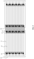
- FIG. 1 is a schematic structural diagram of a back contact solar cell string according to an embodiment of the disclosure.
- FIG. 2 is a schematic structural diagram of a back contact solar cell string according to another embodiment of the disclosure.
- FIG. 3 is a schematic structural diagram of a back contact solar cell string according to still another embodiment of the disclosure.
- FIG. 4 is a schematic structural diagram of a back contact solar cell string according to yet another embodiment of the disclosure.
- FIG. 5 is a schematic structural diagram of a back contact solar cell string according to yet another embodiment of the disclosure.
- FIG. 6 is a schematic structural diagram related to a first bus bar in a back contact solar cell string according to an embodiment of the disclosure.
- FIG. 7 is a flowchart of a method for preparing a back contact solar cell string according to another embodiment of the disclosure.
- connection may be a fixed connection, a detachable connection, or an integral connection; or the connection may be a mechanical connection or an electrical connection; or the connection may be a direct connection, an indirect connection through an intermediary, or internal communication between two components.
- positive electrode regions and negative electrode regions on cell pieces that are not required to be electrically connected are covered by using insulation layers, and first bus bars can be directly connected to all of the positive electrode regions and the negative electrode regions on the cell pieces.
- the insulation layers are disposed, so that the positive electrode regions and the negative electrode regions not required to be electrically connected are insulated from the first bus bars by using the insulation layers, and the positive electrode regions and the negative electrode regions required to be electrically connected are directly electrically connected to the first bus bars.
- the reflection structures are disposed on the first bus bars, so that light can be reflected back to glass in a manufactured cell module, and then reflected to an adjacent cell piece through the glass, and the adjacent cell piece can absorb the light irradiated on the first bus bars. In this way, secondary reflection and utilization of the light irradiated on the cell module can be increased, thereby enhancing the power.
- FIG. 1 is a schematic structural diagram of a back contact solar cell string according to an embodiment of the disclosure. For ease of description, only parts related to this embodiment of the disclosure are shown.
- the back contact solar cell string provided in this embodiment of the disclosure comprises:
- each cell piece comprises positive electrode regions 11 and negative electrode regions 12 alternately disposed;
- insulation layers 13 covering the positive electrode regions 11 on one side of the cell piece and the negative electrode regions 12 on an other side of the cell piece;
- first bus bars 14 connected to two adjacent cell pieces and electrically connected to the positive electrode regions 11 and the negative electrode regions 12 in the two adjacent cell pieces that are not covered by the insulation layers 13 .
- the back contact solar cell string is a cell string formed by serially connecting at least two cell pieces (that is, back contact solar cells) together using the first bus bar 14 disposed between each two cell pieces.
- the cell string may comprise two cell pieces, three cell pieces, or other quantities of cell pieces that are serially connected to each other.
- FIG. 1 , FIG. 3 , FIG. 4 , and FIG. 5 show a cell string formed by two cell pieces serially connected to each other. In this case, only one first bus bar 14 is required to be connected to the two adjacent cell pieces.
- FIG. 2 shows a cell string comprising three cell pieces serially connected to each other. In this case, two first bus bar 14 are required to be respectively connected to the two adjacent cell pieces.
- the cell string may also comprise other quantities of cell pieces serially connected to each other according to actual use requirements, which is not completely shown in the figure.
- the cell string is designed according to actual requirements.
- the cell pieces at two end portions of the cell string are defined as end cell pieces.
- the cell pieces serially connected between the two end cell pieces are defined as internal cell pieces.
- the cell pieces each comprise a front passivation and anti-reflection layer, a silicon substrate, a back tunneling layer, N-type doped regions and P-type doped regions alternately disposed, a back passivation layer, and a cell electrode from top to bottom.
- the N-type doped regions and the P-type doped regions are alternately disposed on a lower surface of the back tunneling layer.
- the cell electrode comprises positive electrode thin grid lines and negative electrode thin grid lines.
- the positive electrode thin grid lines are electrically connected to the P-type doped region to form the positive electrode regions 11 .
- the negative electrode thin grid lines are electrically connected to the N-type doped region to form the negative electrode regions 12 .
- a structure of the cell piece may also be designed differently, which is not limited herein.
- the positive electrode thin grid lines are disposed in the P-type doped region to form the positive electrode regions 11
- the negative electrode thin grid lines are disposed in the N-type doped region to form the negative electrode regions 12
- the positive electrode regions 11 and the negative electrode regions 12 are all disposed on a back side of the cell piece.
- the positive electrode thin grid lines and the negative electrode thin grid lines may extend to end portions of the cell piece.
- a specific distance may be designed between ends of the positive electrode thin grid lines and the negative electrode thin grid lines and the end portions of the cell piece.
- FIG. 1 is a back view of the cell string.
- the cell string comprises a plurality of positive electrode regions 11 and negative electrode regions 12 that are alternately disposed. All of the positive electrode regions 11 and the negative electrode regions 12 are substantially parallel to an edge of the cell piece and are alternately disposed.
- the cell pieces are substantially in rectangular shapes.
- the expression “the cell pieces are substantially rectangular cell pieces” means that, for example, the cell pieces may be in square shapes, or may be in another rectangular shape, and may have standard corners, cut corners, or rounded corner.
- the cell pieces are designed according to actual production requirements, which are not specifically limited herein. Quantities of the positive electrode regions 11 and the negative electrode regions 12 are determined according to actual sizes of the cell pieces and widths of the positive electrode thin grid lines and the negative electrode thin grid lines and distances therebetween, which are not specifically limited herein.
- the positive electrode regions 11 on one side of each cell piece are covered by the insulation layers 13
- the negative electrode regions 12 on another side of each cell piece are also covered by the insulation layers 13 .
- the insulation layers 13 may be insulation pastes, or may be non-conductive adhesive tapes or insulation films, or may be other proper non-conductive shields or covers.
- the insulation layers 13 may comprise materials such as polypropylene, polyethylene, or polyimide, and may further comprise acrylic bonding layers.
- the insulation layers 13 may be in circular shapes, square shapes, triangular shapes, or other shapes.
- the shapes and materials of the insulation layers 13 may be designed according to actual use requirements, provided that the insulation layers can realize insulation between the positive electrode regions 11 or the negative electrode regions 12 that are covered and the outside, which are not specifically limited herein.
- the insulation layers 13 may be preferably spread outward by using ends of the positive electrode regions 11 or the negative electrode regions 12 that are required to be covered as centers.
- the insulation layers 13 may be coated from the ends of the positive electrode regions 11 to the end portions of the cell pieces.
- one region (the positive electrode region 11 or the negative electrode region 12 ) on one side of the cell piece is covered by the insulation layers 13 , and another region is not covered by the insulation layers 13 , so that the region not covered by the insulation layers 13 may be connected to the outside, and the region covered by the insulation layers 13 may be insulated from the outside.
- connection is established from a polarity of a cell piece to another polarity of a next adjacent cell piece by using the first bus bar 14 , to achieve the connection between the cell pieces.
- the first bus bar 14 is electrically connected to the positive electrode regions 11 and the negative electrode regions 12 in the two adjacent cell pieces that are not covered by the insulation layers 13 . That is to say, for example, on the two cell pieces, the positive electrode regions 11 on a left side are covered by the insulation layers 13 and the negative electrode regions 12 on a right side are covered by the insulation layers 13 .
- the negative electrode regions 12 are insulated from the first bus bar 14 by means of the insulation layers 13 disposed on the right side of the end cell piece on a left side, and the positive electrode regions 11 not covered by the insulation layers 13 are electrically connected to the first bus bar 14 .
- the positive electrode regions 11 are insulated from the first bus bar 14 by means of the insulation layers 13 disposed on the left side of the end cell piece on a right side, and the negative electrode regions 12 not covered by the insulation layers 13 are electrically connected to the first bus bar 14 .
- the positive electrode regions 11 of the end cell piece on the left side are connected to the negative electrode regions 12 of the adjacent end cell piece on the right side by using the first bus bar 14 .
- a connection range of the connection between the first bus bar 14 and the two adjacent cell pieces does not exceed a coverage of the insulation layers 13 , so that the first bus bar 14 is insulated from the positive electrode regions 11 or the negative electrode regions 12 that are covered by the insulation layers 13 .
- a current in the negative electrode regions 12 of the end cell piece on the left side flows from inside of the cell piece to the adjacent positive electrode regions 11 .
- the positive electrode regions 11 are electrically connected to the first bus bar 14 , so that a current in the positive electrode regions 11 of the end cell piece on the left side flows to the negative electrode regions 12 of the end cell piece on the right side by using the first bus bar 14 , and further flows from the inside of the end cell piece on the right side to the adjacent positive electrode regions 11 . Therefore, the serial connection between cell pieces is realized. It is to be understood that, when there are 3 or other quantities of cell pieces, the cell pieces are correspondingly electrically connected to each other by using the first bus bars 14 .
- the first bus bars 14 are respectively connected to the positive electrode regions 11 and the negative electrode regions 12 in the respective two adjacent cell pieces that are not covered by the insulation layers 13 .
- first bus bars 14 Left sides of all of the first bus bars 14 are all electrically connected to the positive electrode regions 11 , and right sides of the first bus bars are all electrically connected to the negative electrode regions 12 . Therefore, the serial connection between cell pieces is realized. In this way, the current may flow from one cell piece to the next adjacent cell piece by using the first bus bars 14 , and is finally exported.
- the positive electrode regions 11 and the negative electrode regions 12 on each cell piece that are not covered by the insulation layers 13 may be directly electrically connected to the first bus bar 14 .
- Conductive adhesives or solder pastes 15 are disposed at connection portions between the first bus bar 14 and the positive electrode regions 11 and the negative electrode regions 12 on the cell piece.
- the conductive adhesives or the solder pastes 15 are directly coated in the positive electrode regions 11 and the negative electrode regions 12 on the cell piece that are not covered by the insulation layers 13 .
- the first bus bar 14 can directly come into contact with the conductive adhesives or the solder pastes 15 during connection to the cell piece, so that more desirable electrical connection and physical connection with the positive electrode regions 11 and the negative electrode regions 12 that are required to be connected are realized.
- the conductive adhesives or the solder pastes 15 are required to be successively disposed in each positive electrode region 11 and each negative electrode region 12 that are not covered by the insulation layers 13 , which is relatively cumbersome.
- the conductive adhesives or the solder pastes 15 are required to be coated accurately enough. As shown in FIG.
- the conductive adhesives or the solder pastes 15 are coated on the first bus bar 14 , that is, the conductive adhesives or the solder pastes 15 are disposed on the first bus bar 14 .
- the conductive adhesives or the solder pastes 15 disposed on the first bus bar 14 are merely required to be controlled not to exceed the coverage of the insulation layers 13 .
- the conductive adhesives or the solder pastes 15 may be directly completely and continuously disposed on a periphery of the first bus bar 14 .
- the first bus bar 14 can be electrically connected to each positive electrode region 11 and each negative electrode region 12 that are not covered by the insulation layers 13 more desirably by using the conductive adhesives or the solder pastes 15 .
- the insulation layers 13 even if the conductive adhesives or the solder pastes 15 disposed on the first bus bar 14 cover the insulation layers 13 , the first bus bar is still prevented from being electrically connected to the negative electrode regions 12 or the positive electrode regions 11 that are covered by the insulation layers 13 .
- the negative electrode regions 12 or the positive electrode regions 11 that are covered by the insulation layers 13 are successively covered by the insulation layers 13 , the conductive adhesives or the solder pastes 15 , and the first bus bar 14 . Therefore, coating the conductive adhesives or the solder pastes 15 on the first bus bar 14 is a convenient and rapid process operation.
- busbars or wires 16 connected to each positive electrode region 11 or each negative electrode region 12 that is not covered by the insulation layers 13 are further disposed on each cell piece.
- the negative electrode regions 12 not covered by the insulation layers 13 may be connected to the busbars or the wires 16 . In this way, a current in each negative electrode region 12 may be converged to the busbars or the wires 16 .
- the first bus bar 14 is electrically connected to the positive electrode regions 11 and the negative electrode regions 12 in the two adjacent cell pieces that are not covered by the insulation layers 13 mainly by using the busbars or the wires 16 .
- each positive electrode region 11 or each negative electrode region 12 that is covered by the insulation layers 13 is prevented from being connected to the first bus bar 14 .
- the conductive adhesives or the solder pastes 15 are disposed on the connection portions between the first bus bar 14 and the positive electrode regions 11 and the negative electrode regions 12 on the cell pieces.
- the conductive adhesives or the solder pastes 15 may be coated on the busbars or the wires 16 .
- the conductive adhesives or the solder pastes 15 may be directly coated on the first bus bar 14 .
- the positive electrode regions 11 having a same polarity may all be disposed close to one side, and the negative electrode regions 12 are all disposed close to an other side.
- the positive electrode regions 11 on the left side on the cell piece are coated with the insulation layers 13
- the negative electrode regions 12 on the right side are coated with the insulation layers 13 .
- the negative electrode regions 12 are disposed close to the left side
- the positive electrode regions 11 are disposed close to the right side.
- the negative electrode regions 12 on the left side may be caused to protrude out of the positive electrode regions 11 coated with the insulation layers 13 , so that the negative electrode regions 12 on the left side do not come into contact with the positive electrode regions 11 during connection to the busbars or the wires 16 . Therefore, the positive electrode regions 11 not only realizes insulation from the outside by using the insulation layers 13 covered thereon, but also do not come into contact with the busbars or the wires 16 by means of an offset position.
- the positive electrode regions 11 and the negative electrode regions 12 are all regularly and alternately disposed on a back side of the cell piece. In this case, the insulation layers 13 are required to be coated first, and then the busbars or the wires 16 are disposed.
- solder joints 17 may be further disposed on the busbars or the wires 16 . That is to say, the solder joints 17 are disposed in the positive electrode regions 11 and the negative electrode regions 12 of the cell piece that are electrically connected to the first bus bar 14 .
- a plurality of solder joints 17 are disposed on the busbars or the wires 16 , so as to achieve more desirable electrical connection and physical connection to the first bus bar 14 by using the solder joints 17 .
- a quantity of the solder joints 17 is in a range of 2-20.
- the solder joints 17 may be disposed in part of the positive electrode regions 11 or the negative electrode regions 12 .
- the rest of the positive electrode regions 11 or the negative electrode regions 12 are directly connected to the busbars or the wires 16 .
- the first bus bar 14 is electrically connected to the positive electrode regions 11 and the negative electrode regions 12 in the two adjacent cell pieces that are not covered by the insulation layers 13 respectively by using the solder joints 17 and the busbars or the wires 16 .
- each positive electrode region 11 or each negative electrode region 12 that is covered by the insulation layers 13 is prevented from being connected to the first bus bar 14 .
- the conductive adhesives or the solder pastes 15 are disposed on the connection portions between the first bus bar 14 and the positive electrode regions 11 and the negative electrode regions 12 on the cell pieces.
- the conductive adhesives or the solder pastes 15 may be coated on the solder joints 17 .
- the conductive adhesives or the solder pastes 15 may be directly coated on the first bus bar 14 .
- the first bus bar 14 is a pressure-sensitive conductive adhesive tape or a ribbon.
- the first bus bar 14 comprises a main body portion 141 and extending portions 142 each extending from the main body portion 141 and connected to the positive electrode regions 11 and the negative electrode regions 12 .
- the extending portions 142 extend from the main body portion 141 to form a finger-like shape or a comb-like shape.
- solder joints 17 are alternately disposed, so that the solder joints 17 disposed in the positive electrode regions 11 in a cell piece that are required to be electrically connected correspond to the solder joints 17 disposed in the negative electrode regions 12 in an adjacent cell piece that are required to be electrically connected, thereby achieving corresponding connection between the first bus bar 14 and the solder joints 17 .
- each extending portion 142 is connected to only each positive electrode region 11 or each negative electrode region 12 on the cell piece that is not covered by the insulation layers 13 , and is not connected to each adjacent negative electrode region 12 or each adjacent positive electrode region 11 that is covered by the insulation layers 13 , physical disconnection between the first bus bar 14 and the negative electrode regions 12 or the positive electrode regions 11 that are covered by the insulation layers 13 can be realized on the basis of the insulation layers 13 . In this way, the short circuit caused by the connection between the negative electrode regions 12 or the positive electrode regions 11 that are not completely covered by the insulation layers 13 and the first bus bar 14 is avoided.
- the extending portions may also extend to be fused into a whole.
- the first bus bar 14 may comprise the main body portion and two extending portions extending from two ends of the main body portion.
- the extending portions are connected to the corresponding positive electrode regions 11 or negative electrode regions 12 that are not covered by the insulation layers.
- the positive electrode regions 11 or the negative electrode regions 12 that are covered by the insulation layers 13 are prevented from being connected to the first bus bar 14 .
- a reflection structure 143 is disposed on the main body portion 141 .
- the reflection structure 143 is located in a gap between two adjacent cell pieces. Specifically, during assembling of the cell pieces into a cell module, the two adjacent cell pieces are not completely tightly attached to each other. Instead, a specific gap exists therebetween.
- the reflection structure 143 is disposed on the main body portion 141 , and the reflection structure 143 is located in the gap between the two adjacent cell pieces.
- the extending portions 142 on the two ends of the main body portion 141 are electrically connected to the positive electrode regions 11 and the negative electrode regions 12 in the two adjacent cell pieces that are not covered by the insulation layers 13 , and the reflection structure 143 on the main body portion 141 is accommodated in the gap between the two adjacent cell pieces.
- the reflection structure 143 on the main body portion 141 is accommodated in the gap between the two adjacent cell pieces.
- the reflection structure 143 is a roughly textured structure, a reflective layer coated on the main body portion 141 , or a reflective film attached to the main body portion.
- the reflective film is an aluminum film, a glass bead reflective film, or a microprism reflective film.
- the roughly textured structure comprises but is not limited to a mechanically polished surface, a random pyramid shape, an inverted pyramid shape, a spherical cap shape, a V-shaped groove, and a shape ranging among the above structures.
- the reflective layer and the reflective film may comprise a retroreflection material capable of realizing a reflection effect.
- the reflective layer and the reflective film are designed according to actual use requirements, which are not specifically limited herein.
- the cell string further comprises second bus bars 18 located on end portions of the solar cell string.
- the second bus bars 18 are electrically connected to the positive electrode regions 11 and the negative electrode regions 12 in the cell pieces located on the end portions that are not covered by the insulation layers 13 .
- a quantity of the second bus bars 18 is two.
- the two second bus bars are respectively located on two ends of the two end cell pieces, and are used as two electrodes of the entire cell string. That is to say, a current guided in each positive electrode region 11 and each negative electrode region 12 on each cell piece is serially connected and converged to the two second bus bars 18 on the end portions by using each first bus bar 14 .
- the second bus bars 18 may be electrically connected to the positive electrode regions 11 or the negative electrode regions 12 that are not covered by the insulation layers 13 by using wires, and definitely, may also be in contact with the conductive adhesives or the solder pastes 15 disposed on the first bus bar 14 to be directly connected to the cell pieces, so as to form electrical connection between the second bus bars 18 and the positive electrode regions 11 and the negative electrode regions 12 in the cell pieces located on the end portions that are not covered by the insulation layers 13 .
- the first bus bar 14 and the adjacent cell pieces and the details are not described herein again.
- the positive electrode regions and the negative electrode regions on the cell pieces that are not required to be electrically connected are covered by using the insulation layers, and the first bus bars can be directly connected to all of the positive electrode regions and the negative electrode regions on the cell pieces.
- the insulation layers are disposed, so that the positive electrode regions and the negative electrode regions not required to be electrically connected are insulated from the first bus bars by using the insulation layers, and the positive electrode regions and the negative electrode regions required to be electrically connected are directly electrically connected to the first bus bars.
- the reflection structures are disposed on the first bus bars, so that light can be reflected back to glass in a manufactured cell module, and then reflected to an adjacent cell piece through the glass, and the adjacent cell piece can absorb the light irradiated on the first bus bars. In this way, secondary reflection and utilization of the light irradiated on the cell module can be increased, thereby enhancing the power.
- FIG. 7 is a flowchart of a method for preparing a back contact solar cell string according to a second embodiment of the disclosure. For ease of description, only parts related to this embodiment of the disclosure are shown.
- the preparation method is used for preparing the back contact solar cell string described in the above embodiments. Specifically, the comprises the following steps.
- Step S 11 Respectively dispose an insulation layer in each positive electrode region on one side of each cell piece and in each negative electrode region on another side of each cell piece.
- the positive electrode regions and the negative electrode regions are alternately disposed on a back side of the cell piece.
- the positive electrode regions comprise P-type doped regions and positive electrode thin grid lines disposed in the P-type doped regions.
- the negative electrode regions comprise N-type doped regions and negative electrode thin grid lines disposed in the N-type doped regions.
- insulation layers are disposed on the cell pieces to insulate the positive electrode regions or the negative electrode regions not required to be electrically connected from the outside.
- the insulation layers are uniformly coated to the positive electrode regions on the right side of the cell piece.
- the insulation layers may comprise insulation materials such as polypropylene, polyethylene, or polyimide.
- the insulation layers may be coated by using a printing process, to ensure the accuracy and the quality of the coating.
- the coated insulation layers may be in circular shapes, square shapes, triangular shapes, or other shapes.
- the insulation layers are configured to realize insulation between the positive electrode regions or negative electrode regions that are covered by the insulation layers and the outside, which are not specifically limited herein.
- Step S 21 Connect a first bus bar to the positive electrode regions and the negative electrode regions in two adjacent cell pieces that are not covered by the insulation layers.
- the first bus bar is connected to the positive electrode regions and the negative electrode regions in the two adjacent cell pieces that are not covered by the insulation layers. In this way, the adjacent two cell pieces are electrically connected by using the first bus bar, so as to realize serial connection.
- connecting the first bus bar to the positive electrode regions and the negative electrode regions in the two adjacent cell pieces that are not covered by the insulation layers may be implemented in the following manners.
- Manner I disposing a conductive adhesive or a solder paste in the positive electrode regions and the negative electrode regions on the cell piece that are not covered by the insulation layers;
- Manner II disposing a conductive adhesive or a solder paste on the first bus bar
- the conductive adhesives or the solder pastes are respectively coated on the positive electrode regions and the negative electrode regions on the cell pieces that are not covered by the insulation layers, and then the first bus bar is connected to the two adjacent cell pieces.
- the conductive adhesives or the solder pastes are melted by means of heating and welding such as hot melt welding, laser welding, infrared welding, or electromagnetic welding, and then cured, so that the first bus bar is electrically connected and physically connected to the positive electrode regions and the negative electrode regions in the two adjacent cell pieces that are not covered by the insulation layers.
- Manner II is substantially the same as Manner I, except that the conductive adhesives or the solder pastes are directly disposed on the first bus bar. In this case, the conductive adhesives or the solder pastes disposed on the first bus bar are merely required to be controlled not to exceed a coverage of the insulation layers.
- Manner II the conductive adhesives or the solder pastes are required to be successively disposed in the positive electrode regions and the negative electrode regions that are not covered by the insulation layers, which is relatively cumbersome.
- the conductive adhesives or the solder pastes are required to be coated accurately enough.
- Manner II only the conductive adhesives or the solder pastes are required to be disposed on the first bus bar, so that a process is more convenient and rapid.
- Manner II is preferably selected to connect the first bus bar to the positive electrode regions and the negative electrode regions in the two adjacent cell pieces that are not covered by the insulation layers.
- connecting the first bus bar to the positive electrode regions and the negative electrode regions in the two adjacent cell pieces that are not covered by the insulation layers further comprises:
- the busbars or the wires capable of converging a current are disposed in the positive electrode regions and the negative electrode regions that are not covered by the insulation layers, so that the current in each positive electrode region or each negative electrode region that is not covered by the insulation layers can be converged to the busbars or the wires.
- the first bus bar is connected to the busbars or the wires in the two adjacent cell pieces.
- the positive electrode regions and the negative electrode regions that are covered by the insulation layers are prevented from being connected to the first bus bar, thereby realizing serial connection between the adjacent cell pieces.
- the connection may be implemented in the above Manner II.
- connecting the first bus bar to the positive electrode regions and the negative electrode regions in the two adjacent cell pieces that are not covered by the insulation layers further comprises:
- Solder joints may also be disposed on the busbars or the wires on each cell piece.
- the first bus bar is connected to each solder joint, so that connection between the first bus bar and the positive electrode regions and the negative electrode regions in the two adjacent cell pieces that are not covered by the insulation layers can be realized.
- the connection may be implemented in the above Manner II.
- Step S 31 Connect second bus bars to the positive electrode regions or the negative electrode regions in the cell pieces located on end portions that are not covered by the insulation layers.
- the positive electrode regions or the negative electrode regions in the end cell pieces of the cell string that are not covered by the insulation layers are connected to the second bus bars, to converge the current collected from each cell piece to the second bus bars, so as to form the cell string.
- the step may be specifically electrically connecting the second bus bars to the positive electrode regions or the negative electrode regions that are not covered by the insulation layers by using the wires, or may conform to the connection manner of the first bus bar. Details are not described herein again.
- a third embodiment of the disclosure further provides a cell module.
- the cell module comprises the back contact solar cell string described in the above embodiments.
- an assembling process of the cell module comprises the following.
- Classification of cells since a production line of solar cell pieces is pretty random, the performance of produced cells is not exactly the same. In order to effectively combine cell pieces having same or similar performance together, the cell pieces are required to be classified according to performance parameters measured by means of a cell test, so as to improve the utilization of the cell pieces, thereby manufacturing a qualified cell module.
- the cell test is to test values of output parameters (currents and voltages) of the cells.
- Serial connection the cell pieces are prepared according to the preparation method described in the above method embodiments, so as to form the cell string described in the above device embodiments by means of serial connection.
- Stacking after back sides are serially connected and pass quality inspection, glass, a cut EVA film/POE film, the cell string, an EVA film/POE film, glass fiber, and a back panel/glass are stacked in sequence from bottom to top, where relative positions of the cell string and materials such as the glass are guaranteed during the stacking, and a distance between the cell pieces is adjusted.
- Lamination of module the stacked cell pieces are put into a laminator, the module is vacuumized, then EVA is heated to melt so as to bond the cells, the glass, and the back panel together, and finally, the module is cooled and then taken out.
- the EVA extends outward due to a pressure after being melted and cures, forming rough edges, and therefore the rough edges are required to be cut off after completion of the lamination.
- an aluminum frame is assembled to the module to enhance the strength of the module, so as to further seal the cell module and prolong the service lift of the cell. Gaps between frame and the glass assembly is filled with silicone resin, and the frames are connected to each other by using key joints.
- Bonding of junction box a box is bonded to a wire on a back side of the module, so as to facilitate connection between the cell and other devices or other cells.
- Test of module an output power of the cell is tested and calibrated, and output characteristics thereof are tested, to determine a quality level of the module.
- High voltage test a specific voltage is applied between the frame of the module and the electrode wire, to test a withstand voltage and insulation strength of the module, thereby ensuring that the module is free of damage in daunting natural conditions (such as a lightning stroke).
- a fourth embodiment of the disclosure further provides a photovoltaic system.
- the photovoltaic system comprises the cell module described in the above embodiments.
Landscapes
- Engineering & Computer Science (AREA)
- Computer Hardware Design (AREA)
- Microelectronics & Electronic Packaging (AREA)
- Power Engineering (AREA)
- Physics & Mathematics (AREA)
- Condensed Matter Physics & Semiconductors (AREA)
- Electromagnetism (AREA)
- General Physics & Mathematics (AREA)
- Life Sciences & Earth Sciences (AREA)
- Sustainable Development (AREA)
- Sustainable Energy (AREA)
- Manufacturing & Machinery (AREA)
- Chemical & Material Sciences (AREA)
- Crystallography & Structural Chemistry (AREA)
- Photovoltaic Devices (AREA)
- Connection Of Batteries Or Terminals (AREA)
Abstract
Description
Claims (17)
Applications Claiming Priority (2)
| Application Number | Priority Date | Filing Date | Title |
|---|---|---|---|
| CN202110799134.4 | 2021-07-15 | ||
| CN202110799134.4A CN113327997A (en) | 2021-07-15 | 2021-07-15 | Back contact solar cell string, preparation method, assembly and system |
Publications (2)
| Publication Number | Publication Date |
|---|---|
| US20230021066A1 US20230021066A1 (en) | 2023-01-19 |
| US11728442B2 true US11728442B2 (en) | 2023-08-15 |
Family
ID=77426294
Family Applications (1)
| Application Number | Title | Priority Date | Filing Date |
|---|---|---|---|
| US17/527,090 Active US11728442B2 (en) | 2021-07-15 | 2021-11-15 | Back contact solar cell string and preparation method therefor, module, and system |
Country Status (4)
| Country | Link |
|---|---|
| US (1) | US11728442B2 (en) |
| EP (1) | EP4120366A1 (en) |
| CN (1) | CN113327997A (en) |
| WO (1) | WO2023284100A1 (en) |
Families Citing this family (12)
| Publication number | Priority date | Publication date | Assignee | Title |
|---|---|---|---|---|
| MX2021014279A (en) * | 2019-05-23 | 2022-02-03 | Alpha Assembly Solutions Inc | Solder paste for module fabrication of solar cells. |
| CN113327997A (en) * | 2021-07-15 | 2021-08-31 | 浙江爱旭太阳能科技有限公司 | Back contact solar cell string, preparation method, assembly and system |
| CN114373817B (en) * | 2021-12-28 | 2022-12-16 | 北京博瑞原子空间能源科技有限公司 | Standard module for solar array, preparation method thereof and solar array with standard module |
| CN114122179B (en) * | 2022-01-25 | 2022-09-16 | 浙江爱旭太阳能科技有限公司 | Interdigital back contact cell string, interdigital back contact cell assembly and system |
| CN114242810B (en) * | 2022-02-24 | 2022-04-29 | 广东爱旭科技有限公司 | Electrode structure of back contact battery, assembly and battery system |
| CN114649443B (en) * | 2022-03-03 | 2024-04-16 | 浙江爱旭太阳能科技有限公司 | Back contact solar cell string, preparation method thereof, cell assembly and photovoltaic system |
| CN115172499B (en) * | 2022-06-07 | 2024-03-29 | 深圳赛能数字能源技术有限公司 | Back contact battery, manufacturing method thereof, battery assembly and photovoltaic system |
| CN115172494A (en) * | 2022-07-01 | 2022-10-11 | 浙江爱旭太阳能科技有限公司 | IBC battery pack packaging process and IBC battery pack |
| CN115312613A (en) * | 2022-08-29 | 2022-11-08 | 晶澳(扬州)太阳能科技有限公司 | Interconnection belt, solar cell module and preparation method of solar cell module |
| CN116995135B (en) * | 2023-08-03 | 2024-03-08 | 南京晓庄学院 | Photovoltaic module backboard packaging method based on solar photovoltaic power generation |
| CN118039521B (en) * | 2024-04-11 | 2024-07-02 | 滁州捷泰新能源科技有限公司 | Device and method for testing insulation property of thin grid of battery piece and preparation method of back contact assembly |
| CN118116991B (en) * | 2024-04-28 | 2024-09-13 | 浙江晶科能源有限公司 | Photovoltaic module and method for manufacturing same |
Citations (11)
| Publication number | Priority date | Publication date | Assignee | Title |
|---|---|---|---|---|
| US20080216887A1 (en) * | 2006-12-22 | 2008-09-11 | Advent Solar, Inc. | Interconnect Technologies for Back Contact Solar Cells and Modules |
| US20090183759A1 (en) * | 2008-01-21 | 2009-07-23 | Sanyo Electric Co., Ltd. | Solar cell module |
| US20100031999A1 (en) * | 2008-08-08 | 2010-02-11 | Sanyo Electric Co., Ltd. | Solar cell module |
| US20110120530A1 (en) * | 2007-08-23 | 2011-05-26 | Takayuki Isaka | Back surface contact type solar cell, back surface contact type solar cell with wiring board, solar cell string, and solar cell module |
| EP2575184A2 (en) | 2011-09-29 | 2013-04-03 | LG Electronics Inc. | Solar cell module |
| CN103928555A (en) * | 2014-05-05 | 2014-07-16 | 友达光电股份有限公司 | Solar battery module |
| US20150059831A1 (en) * | 2012-05-09 | 2015-03-05 | Sanyo Electric Co., Ltd. | Solar cell module |
| EP2958152A1 (en) | 2014-06-18 | 2015-12-23 | LG Electronics Inc. | Solar cell module |
| CN106098831A (en) | 2016-08-02 | 2016-11-09 | 泰州中来光电科技有限公司 | A kind of back contact solar cell string and preparation method thereof and assembly, system |
| US20180204968A1 (en) * | 2016-03-21 | 2018-07-19 | SUZHOU COOP&INNO GREEN ENERGY TECHNOLOGY Co.,Ltd | Back-Contact Cell Module and Method of Manufacturing Same |
| EP3608974A1 (en) | 2017-04-01 | 2020-02-12 | Jolywood (Taizhou) Solar Technology Co., Ltd. | Cell string formed by connecting n-type ibc solar cells in spliced-sheet manner, preparation method therefor, assembly and system |
Family Cites Families (4)
| Publication number | Priority date | Publication date | Assignee | Title |
|---|---|---|---|---|
| EP2068369A1 (en) * | 2007-12-03 | 2009-06-10 | Interuniversitair Microelektronica Centrum (IMEC) | Photovoltaic cells having metal wrap through and improved passivation |
| CN209344099U (en) * | 2018-12-12 | 2019-09-03 | 广东汉能薄膜太阳能有限公司 | A kind of Thinfilm solar cell assembly |
| CN111599885A (en) * | 2020-06-10 | 2020-08-28 | 晶澳(扬州)太阳能科技有限公司 | Solar cell module and preparation method |
| CN113327997A (en) * | 2021-07-15 | 2021-08-31 | 浙江爱旭太阳能科技有限公司 | Back contact solar cell string, preparation method, assembly and system |
-
2021
- 2021-07-15 CN CN202110799134.4A patent/CN113327997A/en active Pending
- 2021-09-09 WO PCT/CN2021/117487 patent/WO2023284100A1/en active Application Filing
- 2021-11-15 US US17/527,090 patent/US11728442B2/en active Active
- 2021-11-16 EP EP21000332.3A patent/EP4120366A1/en active Pending
Patent Citations (11)
| Publication number | Priority date | Publication date | Assignee | Title |
|---|---|---|---|---|
| US20080216887A1 (en) * | 2006-12-22 | 2008-09-11 | Advent Solar, Inc. | Interconnect Technologies for Back Contact Solar Cells and Modules |
| US20110120530A1 (en) * | 2007-08-23 | 2011-05-26 | Takayuki Isaka | Back surface contact type solar cell, back surface contact type solar cell with wiring board, solar cell string, and solar cell module |
| US20090183759A1 (en) * | 2008-01-21 | 2009-07-23 | Sanyo Electric Co., Ltd. | Solar cell module |
| US20100031999A1 (en) * | 2008-08-08 | 2010-02-11 | Sanyo Electric Co., Ltd. | Solar cell module |
| EP2575184A2 (en) | 2011-09-29 | 2013-04-03 | LG Electronics Inc. | Solar cell module |
| US20150059831A1 (en) * | 2012-05-09 | 2015-03-05 | Sanyo Electric Co., Ltd. | Solar cell module |
| CN103928555A (en) * | 2014-05-05 | 2014-07-16 | 友达光电股份有限公司 | Solar battery module |
| EP2958152A1 (en) | 2014-06-18 | 2015-12-23 | LG Electronics Inc. | Solar cell module |
| US20180204968A1 (en) * | 2016-03-21 | 2018-07-19 | SUZHOU COOP&INNO GREEN ENERGY TECHNOLOGY Co.,Ltd | Back-Contact Cell Module and Method of Manufacturing Same |
| CN106098831A (en) | 2016-08-02 | 2016-11-09 | 泰州中来光电科技有限公司 | A kind of back contact solar cell string and preparation method thereof and assembly, system |
| EP3608974A1 (en) | 2017-04-01 | 2020-02-12 | Jolywood (Taizhou) Solar Technology Co., Ltd. | Cell string formed by connecting n-type ibc solar cells in spliced-sheet manner, preparation method therefor, assembly and system |
Also Published As
| Publication number | Publication date |
|---|---|
| US20230021066A1 (en) | 2023-01-19 |
| EP4120366A1 (en) | 2023-01-18 |
| WO2023284100A1 (en) | 2023-01-19 |
| CN113327997A (en) | 2021-08-31 |
Similar Documents
| Publication | Publication Date | Title |
|---|---|---|
| US11728442B2 (en) | Back contact solar cell string and preparation method therefor, module, and system | |
| US11482632B1 (en) | Back contact solar cell string and preparation method therefor, module, and sytsem | |
| US8927850B2 (en) | Photovoltaic module | |
| JP2019004155A (en) | High efficiency configuration for solar cell string | |
| WO2012001815A1 (en) | Solar cell module and method for manufacturing same | |
| US9202957B2 (en) | Photoelectric converter device and method for its manufacture | |
| US20120291850A1 (en) | Concentrating solar battery, concentrating solar battery module, concentrating solar battery system, method for manufacturing concentrating solar battery, and method for manufacturing concentrating solar battery module | |
| JP2004055596A (en) | Method of manufacturing solar cell module, and solar cell module panel using same | |
| WO2012002422A1 (en) | Method for manufacturing solar cell module, and solar cell module manufactured by the method | |
| US20180366606A1 (en) | Solar cell module | |
| WO2012162900A1 (en) | Solar cell module and manufacturing method thereof | |
| CN214753809U (en) | Back contact solar cell string, assembly and system | |
| US20170373210A1 (en) | Solar cell module | |
| US20120247529A1 (en) | Solar cell modules and methods of manufacturing the same | |
| WO2018176182A1 (en) | Cell string formed by connecting n-type ibc solar cells in spliced-sheet manner, preparation method therefor, assembly and system | |
| CN214898458U (en) | Back contact solar cell string, assembly and system | |
| CN118099240A (en) | Back contact battery assembly, manufacturing method thereof and photovoltaic power generation system | |
| TWI669828B (en) | Solar battery module, solar battery module manufacturing method and wire | |
| CN110718600A (en) | Heterojunction battery and subassembly packaging structure thereof | |
| CN113644145B (en) | Solar cell and photovoltaic module | |
| NL2033481A (en) | Photovoltaic module | |
| US11791431B2 (en) | Back contact solar cell string and preparation method therefor, module, and system | |
| CN221407333U (en) | Welding strip, battery string, battery assembly and photovoltaic system | |
| US20240243210A1 (en) | Photovoltaic module and method for manufacturing photovoltaic module | |
| CN118156332A (en) | Back contact battery assembly, manufacturing method thereof and photovoltaic power generation system |
Legal Events
| Date | Code | Title | Description |
|---|---|---|---|
| AS | Assignment |
Owner name: GUANGDONG AIKO SOLAR ENERGY TECHNOLOGY CO., LTD., CHINA Free format text: ASSIGNMENT OF ASSIGNORS INTEREST;ASSIGNORS:DAI, WEI;YANG, XINQIANG;CHEN, GANG;REEL/FRAME:058830/0622 Effective date: 20211108 Owner name: TIANJIN AIKO SOLAR ENERGY TECHNOLOGY CO., LTD., CHINA Free format text: ASSIGNMENT OF ASSIGNORS INTEREST;ASSIGNORS:DAI, WEI;YANG, XINQIANG;CHEN, GANG;REEL/FRAME:058830/0622 Effective date: 20211108 Owner name: ZHUHAI FUSHAN AIKO SOLAR ENERGY TECHNOLOGY CO., LTD., CHINA Free format text: ASSIGNMENT OF ASSIGNORS INTEREST;ASSIGNORS:DAI, WEI;YANG, XINQIANG;CHEN, GANG;REEL/FRAME:058830/0622 Effective date: 20211108 Owner name: ZHEJIANG AIKO SOLAR ENERGY TECHNOLOGY CO., LTD., CHINA Free format text: ASSIGNMENT OF ASSIGNORS INTEREST;ASSIGNORS:DAI, WEI;YANG, XINQIANG;CHEN, GANG;REEL/FRAME:058830/0622 Effective date: 20211108 |
|
| FEPP | Fee payment procedure |
Free format text: ENTITY STATUS SET TO UNDISCOUNTED (ORIGINAL EVENT CODE: BIG.); ENTITY STATUS OF PATENT OWNER: LARGE ENTITY |
|
| STPP | Information on status: patent application and granting procedure in general |
Free format text: NON FINAL ACTION MAILED |
|
| STPP | Information on status: patent application and granting procedure in general |
Free format text: PUBLICATIONS -- ISSUE FEE PAYMENT RECEIVED |
|
| STPP | Information on status: patent application and granting procedure in general |
Free format text: PUBLICATIONS -- ISSUE FEE PAYMENT VERIFIED |
|
| STCF | Information on status: patent grant |
Free format text: PATENTED CASE |