EP4099330A1 - Procédé de test de puce de mémoire, dispositif informatique et support - Google Patents
Procédé de test de puce de mémoire, dispositif informatique et support Download PDFInfo
- Publication number
- EP4099330A1 EP4099330A1 EP21876735.8A EP21876735A EP4099330A1 EP 4099330 A1 EP4099330 A1 EP 4099330A1 EP 21876735 A EP21876735 A EP 21876735A EP 4099330 A1 EP4099330 A1 EP 4099330A1
- Authority
- EP
- European Patent Office
- Prior art keywords
- data strobe
- state
- memory chip
- test
- resistance value
- Prior art date
- Legal status (The legal status is an assumption and is not a legal conclusion. Google has not performed a legal analysis and makes no representation as to the accuracy of the status listed.)
- Pending
Links
Images


Classifications
-
- G—PHYSICS
- G11—INFORMATION STORAGE
- G11C—STATIC STORES
- G11C29/00—Checking stores for correct operation ; Subsequent repair; Testing stores during standby or offline operation
- G11C29/02—Detection or location of defective auxiliary circuits, e.g. defective refresh counters
- G11C29/022—Detection or location of defective auxiliary circuits, e.g. defective refresh counters in I/O circuitry
-
- G—PHYSICS
- G11—INFORMATION STORAGE
- G11C—STATIC STORES
- G11C29/00—Checking stores for correct operation ; Subsequent repair; Testing stores during standby or offline operation
- G11C29/56—External testing equipment for static stores, e.g. automatic test equipment [ATE]; Interfaces therefor
- G11C29/56012—Timing aspects, clock generation, synchronisation
-
- G—PHYSICS
- G11—INFORMATION STORAGE
- G11C—STATIC STORES
- G11C29/00—Checking stores for correct operation ; Subsequent repair; Testing stores during standby or offline operation
- G11C29/04—Detection or location of defective memory elements, e.g. cell constructio details, timing of test signals
- G11C29/08—Functional testing, e.g. testing during refresh, power-on self testing [POST] or distributed testing
- G11C29/12—Built-in arrangements for testing, e.g. built-in self testing [BIST] or interconnection details
- G11C29/1201—Built-in arrangements for testing, e.g. built-in self testing [BIST] or interconnection details comprising I/O circuitry
-
- G—PHYSICS
- G11—INFORMATION STORAGE
- G11C—STATIC STORES
- G11C29/00—Checking stores for correct operation ; Subsequent repair; Testing stores during standby or offline operation
- G11C29/04—Detection or location of defective memory elements, e.g. cell constructio details, timing of test signals
- G11C29/50—Marginal testing, e.g. race, voltage or current testing
- G11C29/50008—Marginal testing, e.g. race, voltage or current testing of impedance
Definitions
- the disclosure relates to the field of chip test technologies, and specifically, to a method for testing a memory chip, a computer device, and a medium.
- the chip packages may generally be categorized into different types according to a packaging material of a chip package, a connection manner between a chip package and a Printed Circuit Board (PCB), and the appearance of a chip package. Different types of chip packages have different test methods and different test procedures.
- PCB Printed Circuit Board
- Common test terminals for a memory chip package generally include a data terminal, a power source terminal, a data strobe terminal, a complementary data strobe terminal, and the like. Restricted by structural properties and functional parameters of a memory chip, a current signal or a voltage signal acquired by the data strobe terminal or the complementary data strobe terminal of the memory chip is generally a pulse signal, and cannot be directly used to test electrical performance parameters of the memory chip. As a result, the data strobe terminal and the complementary data strobe terminal of the memory chip have test blind spots.
- An aspect of the disclosure provides a method for testing a memory chip, including:
- a memory chip is controlled to control, in response to a read command for the memory chip, a clock signal of the memory chip to be kept in a first state such as a high level state within a first preset time period and at the same time control a complementary clock signal of the memory chip to be kept in a second state such as a low level state within the first preset time period, the first state and the second state being opposite states.
- the memory chip is controlled to respond to the read command for the memory chip, to enable the memory chip to keep, in response to the clock signal kept in the first state and the complementary clock signal kept in the second state, a data strobe signal in the first state within a second preset time period and at the same time keep a complementary data strobe signal in the second state within the second preset time period, the data strobe signal being outputted by a data strobe terminal of the memory chip, the complementary data strobe signal being outputted by a complementary data strobe terminal of the memory chip, so that while the data strobe signal is kept in the first state and the complementary data strobe signal is kept in the second state, a first driving module connected to the data strobe terminal is controlled to operate and measure a first resistance value and a second driving module connected to the complementary data strobe terminal is controlled to operate and measure a second resistance value.
- a read command for the memory chip is sent to a memory chip, the memory chip is controlled to keep a clock signal in a first state within a first preset time period and keep a complementary clock signal in a second state within the first preset time period, and a data strobe signal is kept in the first state within a second preset time period and at the same time a complementary data strobe signal is kept in the second state within the second preset time period, so that a test current or a test voltage can be acquired by a data strobe terminal and a complementary data strobe terminal, a first driving module connected to the data strobe terminal operates and measures a first resistance value, and the second driving module connected to the complementary data strobe terminal operates and measures a second resistance value, to determine, according to the measured first resistance value and second resistance value, whether there is an anomaly in the memory chip.
- the test method in this embodiment is simple and has low costs and an adequate test effect.
- Another aspect of the disclosure provides a computer device, including a memory and a processor, the memory storing a computer program executable on the processor, the processor executing the computer program to implement the steps in the method for testing a memory chip in any embodiment of the disclosure.
- Still another aspect of the disclosure provides a computer-readable storage medium, storing a computer program, the computer program being executed by a processor to implement the steps in the method for testing a memory chip in any embodiment of the disclosure.
- a data strobe terminal and a complementary data strobe terminal of the semiconductor memory chip package may be configured to test electrical performance parameters of a semiconductor memory chip.
- a data strobe signal DQS acquired by the data strobe terminal and a complementary data strobe signal DQSn acquired by the complementary data strobe terminal are shown as pulse square wave signals in FIG. 1 , and as a result cannot be directly used for testing electrical performance parameters of a memory chip, and the data strobe terminal and the complementary data strobe terminal of the memory chip have test blind spots.
- a method for testing a memory chip including the following steps.
- step 22 in response to a read command for the memory chip, a clock signal is controlled to be kept in a first state within a first preset time period and at the same time a complementary clock signal is controlled to be kept in a second state within the first preset time period, the first state and the second state being opposite states.
- step 24 in response to the clock signal kept in the first state and the complementary clock signal kept in the second state, a data strobe signal is kept in the first state within a second preset time period and at the same time a complementary data strobe signal is kept in the second state within the second preset time period, the data strobe signal being outputted by a data strobe terminal of a memory chip, the complementary data strobe signal being outputted by a complementary data strobe terminal of the memory chip.
- step 26 when the data strobe signal is kept in the first state and the complementary data strobe signal is kept in the second state, a first driving module connected to the data strobe terminal is controlled to operate and measure a first resistance value and a second driving module connected to the complementary data strobe terminal is controlled to operate and measure a second resistance value.
- the clock signal of the memory chip is controlled to be kept in the first state such as a high level state within the first preset time period and at the same time the complementary clock signal of the memory chip is controlled to be kept in the second state such as a low level state within the first preset time period, the first state and the second state being opposite states.
- the clock signal is inputted into the memory chip through a clock terminal port of the memory chip, and the complementary clock signal is inputted into the memory chip through a complementary clock terminal port of the memory chip.
- the memory chip is controlled to respond to the read command for the memory chip, to enable the memory chip to keep, in response to the clock signal kept in the first state and the complementary clock signal kept in the second state, a data strobe signal in the first state within a second preset time period and at the same time keep a complementary data strobe signal in the second state within the second preset time period, the data strobe signal being outputted by a data strobe terminal of the memory chip, the complementary data strobe signal being outputted by a complementary data strobe terminal of the memory chip, so that while the data strobe signal is kept in the first state and the complementary data strobe signal is kept in the second state, the first driving module connected to the data strobe terminal is controlled to operate and measure the first resistance value and the second driving module connected to the complementary data strobe terminal is controlled to operate and measure the second resistance value.
- a read command for the memory chip is sent to a memory chip, the memory chip is controlled to keep a clock signal in a first state within a first preset time period and keep a complementary clock signal in a second state within the first preset time period, and a data strobe signal is kept in the first state within a second preset time period and at the same time a complementary data strobe signal is kept in the second state within the second preset time period, so that a test current or a test voltage can be acquired by a data strobe terminal and a complementary data strobe terminal, a first driving module connected to the data strobe terminal operates and measures a first resistance value, and a second driving module connected to the complementary data strobe terminal operates and measures a second resistance value, to determine, according to the measured first resistance value and second resistance value, whether there is an anomaly in the memory chip.
- the test method in this embodiment is simple and has low costs and an adequate test effect.
- the memory chip is controlled to respond to a read command for the memory chip Read CMD, and a clock signal CK of the memory chip is controlled to be kept in a high level state within the first preset time period and at the same time a complementary clock signal CKn of the memory chip is controlled to be kept in a low level state within the first preset time period.
- a clock signal CK of the memory chip is controlled to be kept in a high level state within the first preset time period and at the same time a complementary clock signal CKn of the memory chip is controlled to be kept in a low level state within the first preset time period.
- the first driving module connected to the data strobe terminal is controlled to operate and measure the first resistance value
- the second driving module connected to the complementary data strobe terminal is controlled to operate and measure the second resistance value
- the read command for the memory chip Read CMD is sent to the memory chip, the clock signal CK of the memory chip is controlled to be kept in a high level state within the first preset time period, and the complementary clock signal CKn is kept in a low level state within the first preset time period, to keep the data strobe signal in a high level state within the second preset time period and at the same time keep the complementary data strobe signal in a low level state within the second preset time period, so that a test current or a test voltage can be acquired by a data strobe terminal and a complementary data strobe terminal, the first driving module connected to the data strobe terminal operates and measures the first resistance value, and the second driving module connected to the complementary data strobe terminal operates and measures the second resistance value, to determine, according to the measured first resistance value and second resistance value, whether there is an anomaly in the memory chip.
- the test method in this embodiment is simple and has low costs and an adequate test effect.
- a time difference between a starting point t2 of the second preset time period and a starting point t1 of the first preset time period is an integer multiple of a value T of a clock period of the clock signal CK.
- a clock circuit such as a DLL circuit and/or a PLL circuit in the memory chip may enable a data strobe signal DQS to be kept in the first state and at the same time enable the complementary data strobe signal DQSn to be kept in the second state. That is, in the disclosure, inherent properties of a circuit inside the memory chip are used to implement the control of the data strobe signal DQS and the complementary data strobe signal DQSn, to enable a first driving circuit connected to the data strobe terminal to operate and measure the first resistance value and a second driving circuit connected to the complementary data strobe terminal to operate and measure the second resistance value.
- step 26 includes the following steps.
- step 261 when the data strobe signal is kept in the first state and the complementary data strobe signal is kept in the second state, the first driving module is controlled to act and provide a first test voltage to the data strobe terminal of the memory chip.
- step 262 the data strobe terminal acquires a first test current when the memory chip is jointly driven by a power source voltage and the first test voltage.
- the first resistance value is calculated according to the power source voltage, the first test voltage and the first test current.
- the first driving module may be controlled to act and provide a first test voltage to the data strobe terminal of the memory chip, and the data strobe terminal acquires the first test current when the memory chip is jointly driven by the power source voltage and the first test voltage.
- a method for testing a memory chip including the following steps.
- step 22 in response to a read command for the memory chip, a clock signal is controlled to be kept in a first state within a first preset time period and at the same time a complementary clock signal is controlled to be kept in a second state within the first preset time period, the first state and the second state being opposite states.
- step 24 in response to the clock signal kept in the first state and the complementary clock signal kept in the second state, a data strobe signal is kept in the first state within a second preset time period and at the same time a complementary data strobe signal is kept in the second state within the second preset time period, the data strobe signal being outputted by a data strobe terminal of a memory chip, the complementary data strobe signal being outputted by a complementary data strobe terminal of the memory chip.
- step 261 when the data strobe signal is kept in the first state and the complementary data strobe signal is kept in the second state, the first driving module is controlled to act and provide a first test voltage to the data strobe terminal of the memory chip.
- step 2621 a first sampled test current when the memory chip is jointly driven by the power source voltage and the first test voltage is acquired by the data strobe terminal.
- step 2622 an average of amplitudes of the first sampled test current within a first preset sampling time period is acquired, and it is determined whether the average is greater than or equal to a first preset current threshold.
- step 2623 if the average is greater than or equal to the first preset current threshold, the average of the amplitudes of the first sampled test current is outputted.
- the first resistance value is calculated according to the power source voltage, the first test voltage and the average of the amplitudes of the first sampled test current.
- the average of the amplitudes of the first sampled test current within the first preset sampling time period is acquired, and a first sampled test current with an average being greater than or equal to the first preset current threshold is acquired, to prevent excessive noise signals in the acquired first sampled test current, thereby avoiding affecting the accuracy of the first resistance value calculated according to the power source voltage, the first test voltage and the first test current.
- the calculating the first resistance value according to the power source voltage, the first test voltage and the average of the amplitudes of the first sampled test current includes:
- an output driving circuit when the memory chip is in a read data mode (an output driving mode) in response to the read command, an output driving circuit operates, a pull-up driving circuit operates, a pull-down driving circuit is turned off, and the pull-up driving circuit enables a data strobe terminal DQS to output a high level.
- the pull-up driving circuit is turned on, that is, the first driving module operates, and provides a first test voltage V Test1 to the data strobe terminal DQS, to measure equivalent resistance R pu of the pull-up driving circuit, that is, the first driving module according to Formula (1).
- step 24 differences between this embodiment of the disclosure and the embodiment shown in FIG. 5 lie in that, after step 24, the method further includes the following steps.
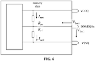
- step 264 when the data strobe signal is kept in the first state and the complementary data strobe signal is kept in the second state, the second driving module is controlled to act and provide a second test voltage to the complementary data strobe terminal of the memory chip.
- step 265 a second test current when the memory chip is driven by the second test voltage is acquired by the complementary data strobe terminal.
- step 266 the second resistance value is calculated according to the second test voltage and the second test current.
- the second driving module is controlled to act and provide the second test voltage to the complementary data strobe terminal of the memory chip, to calculate the second resistance value according to the second test voltage and the second test current.
- step 264 differences between this embodiment of the disclosure and the embodiment shown in FIG. 6 lie in that, after step 264, the method further includes the following steps.
- step 2651 a second sampled test current when the memory chip is driven by the second test voltage is acquired by the complementary data strobe terminal.
- step 2652 an average of amplitudes of the second sampled test current within a second preset sampling time period is acquired, and it is determined whether the average is greater than or equal to a second preset current threshold.
- step 2653 if the average is greater than or equal to the second preset current threshold, the average of the amplitudes of the second sampled test current is outputted.
- step 2661 the second resistance value is calculated according to the second test voltage and the average of the amplitudes of the second sampled test current.
- the obtained average of the amplitudes of the second sampled test current within the second preset sampling time period is acquired, and a second sampled test current with an average being greater than or equal to the second preset current threshold is acquired, to prevent excessive noise signals in the acquired second sampled test current, thereby avoiding affecting the accuracy of the second resistance value calculated according to the second test voltage and the second test current.
- the calculating the second resistance value according to the second test voltage and the average of the amplitudes of the second sampled test current includes:
- an output driving circuit when the memory chip is in a read data mode (an output driving mode) in response to the read command, an output driving circuit operates, a pull-down driving circuit operates, a pull-up driving circuit is turned off, and the pull-down driving circuit enables a complementary data strobe terminal DQSn to output a low level.
- the pull-down driving circuit is turned on, that is, the second driving module operates, and provides the second test voltage V Test2 to the complementary data strobe terminal DQSn, to measure the equivalent resistance R pd of the pull-down driving circuit, that is, a second driving circuit according to Formula (2).
- the method for testing a memory chip further includes the following step.
- step 267 when the clock signal is kept in the second state and the complementary clock signal is kept in the first state, a third driving module connected to the data strobe terminal is controlled to operate and measure a third resistance value, and a fourth driving module connected to the complementary data strobe terminal is controlled to operate and measure a fourth resistance value.
- the first driving module connected to the data strobe terminal may be controlled to operate and measure the first resistance value and the second driving module connected to the complementary data strobe terminal may be controlled to operate and measure the second resistance value.
- the third driving module connected to the data strobe terminal is controlled to operate and measure the third resistance value; and the fourth driving module connected to the complementary data strobe terminal is controlled to operate and measure the fourth resistance value.
- comprehensive test of the memory chip can be implemented by the data strobe terminal and the complementary data strobe terminal.
- the first resistance value and the fourth resistance value acquired in two test processes may be compared, and the second resistance value and the third resistance value are compared, to assist in determining whether there is an anomaly in the memory chip.
- the first resistance value and the fourth resistance value are both equivalent resistance values obtained by measuring the pull-up driving circuit, and the second resistance value and the third resistance value are both equivalent resistance values obtained by measuring the pull-down driving circuit.
- a computer device may be a terminal, and an internal structural diagram of the terminal may be shown in FIG. 10 .
- the computer device includes a processor, a memory, a network interface, a display screen and an input device that are connected by a system bus.
- the processor of the computer device is configured to provide a computing and control capability.
- the memory of the computer device includes a non-volatile storage medium and internal memory.
- the non-volatile storage medium stores an operating system and a computer program.
- the computer program is executed by the processor to implement a method for testing a memory chip.
- the display screen of the computer device may be a liquid crystal display screen or an e-ink display screen.
- the input device of the computer device may be a touch layer covering the display screen, or may be a button, a trackball or a touchpad disposed on a housing of the computer device, or may be an external keyboard, a touchpad or mouse or the like.
- FIG. 10 is only a block diagram of a partial structure related to the solution of the disclosure, but does not constitute a limitation to the computer device on which the solution of the disclosure is applied.
- the specific computer device may include more or fewer components than those shown in the drawings, or some components may be combined, or different component arrangements are used.
- a computer-readable storage medium storing a computer program, the computer program being executed by a processor to implement the steps in the method for testing a memory chip in any embodiment of the disclosure.
- the computer program may be stored in a non-volatile computer-readable storage medium.
- the computer program is executed to perform the procedures in the foregoing embodiments of the methods.
- Any usage of a memory, storage, a database or another medium in the embodiments of the disclosure may include non-volatile and/or volatile memories.
- the non-volatile memory may include a read-only memory (ROM), a programmable ROM (PROM), an electrically programmable ROM (EPROM), an electrically erasable programmable ROM (EEPROM) or a flash memory.
- the volatile memory may include a random access memory (RAM) or an external cache memory.
- the RAM may be in various forms, for example, a static RAM (SRAM), a dynamic RAM (DRAM), a synchronous DRAM (SDRAM), a double data rate SDRAM (DDRSDRAM), an enhanced SDRAM (ESDRAM), a Synchlink DRAM (SLDRAM), a Rambus direct RAM (RDRAM), a Direct Rambus Dynamic RAM (DRDRAM), and a memory bus dynamic RAM (RDRAM).
- SRAM static RAM
- DRAM dynamic RAM
- SDRAM synchronous DRAM
- DDRSDRAM double data rate SDRAM
- ESDRAM enhanced SDRAM
- SLDRAM Synchlink DRAM
- RDRAM Rambus direct RAM
- DRAM Direct Rambus Dynamic RAM
- RDRAM memory bus dynamic RAM
Landscapes
- Tests Of Electronic Circuits (AREA)
Applications Claiming Priority (2)
| Application Number | Priority Date | Filing Date | Title |
|---|---|---|---|
| CN202110441989.XA CN115240748A (zh) | 2021-04-23 | 2021-04-23 | 存储芯片测试方法、计算机设备及介质 |
| PCT/CN2021/112894 WO2022222327A1 (fr) | 2021-04-23 | 2021-08-17 | Procédé de test de puce de mémoire, dispositif informatique et support |
Publications (2)
| Publication Number | Publication Date |
|---|---|
| EP4099330A1 true EP4099330A1 (fr) | 2022-12-07 |
| EP4099330A4 EP4099330A4 (fr) | 2023-06-07 |
Family
ID=83693389
Family Applications (1)
| Application Number | Title | Priority Date | Filing Date |
|---|---|---|---|
| EP21876735.8A Pending EP4099330A4 (fr) | 2021-04-23 | 2021-08-17 | Procédé de test de puce de mémoire, dispositif informatique et support |
Country Status (2)
| Country | Link |
|---|---|
| US (1) | US11721411B2 (fr) |
| EP (1) | EP4099330A4 (fr) |
Family Cites Families (9)
| Publication number | Priority date | Publication date | Assignee | Title |
|---|---|---|---|---|
| JP4075140B2 (ja) | 1998-06-25 | 2008-04-16 | 富士通株式会社 | 電子装置及び半導体記憶装置 |
| JP2000074986A (ja) * | 1998-08-31 | 2000-03-14 | Ando Electric Co Ltd | デバイス試験装置 |
| KR100557636B1 (ko) | 2003-12-23 | 2006-03-10 | 주식회사 하이닉스반도체 | 클럭신호를 이용한 데이터 스트로브 회로 |
| KR100605590B1 (ko) | 2004-05-10 | 2006-07-31 | 주식회사 하이닉스반도체 | 데이터 출력드라이버의 임피던스를 조정할 수 있는 반도체메모리 장치 |
| JP2007036546A (ja) * | 2005-07-26 | 2007-02-08 | Nec Electronics Corp | インピーダンス調整回路と方法 |
| KR100640158B1 (ko) * | 2005-09-27 | 2006-11-01 | 주식회사 하이닉스반도체 | 데이터 출력드라이버의 임피던스를 조정할 수 있는 반도체메모리 장치 |
| KR100733430B1 (ko) | 2005-09-29 | 2007-06-29 | 주식회사 하이닉스반도체 | 반도체 메모리 장치 |
| CN106875966B (zh) | 2017-01-09 | 2020-02-07 | 上海兆芯集成电路有限公司 | 数据选通信号处理系统以及处理方法 |
| US10803914B1 (en) | 2019-08-27 | 2020-10-13 | Micron Technology, Inc. | Selectively squelching differential strobe input signal in memory-device testing system |
-
2021
- 2021-08-17 EP EP21876735.8A patent/EP4099330A4/fr active Pending
-
2022
- 2022-02-11 US US17/669,520 patent/US11721411B2/en active Active
Also Published As
| Publication number | Publication date |
|---|---|
| US11721411B2 (en) | 2023-08-08 |
| EP4099330A4 (fr) | 2023-06-07 |
| US20220343997A1 (en) | 2022-10-27 |
Similar Documents
| Publication | Publication Date | Title |
|---|---|---|
| US7852099B1 (en) | Frequency trimming for internal oscillator for test-time reduction | |
| US7607060B2 (en) | System and method for performing high speed memory diagnostics via built-in-self-test | |
| EP2015309A1 (fr) | Dispositif d'oscillation, procédé de réglage de celui-ci et mémoire | |
| CN108009372B (zh) | 一种ddr内存虚拟写电平校准响应的方法 | |
| US8619935B2 (en) | Methods and structure for on-chip clock jitter testing and analysis | |
| EP3244224B1 (fr) | Système et procédé intégrés pour tester la marge de synchronisation d'un système | |
| US6871306B2 (en) | Method and device for reading and for checking the time position of data response signals read out from a memory module to be tested | |
| EP4099330A1 (fr) | Procédé de test de puce de mémoire, dispositif informatique et support | |
| US6876219B2 (en) | Test configuration with automatic test machine and integrated circuit and method for determining the time behavior of an integrated circuit | |
| JPH027530B2 (fr) | ||
| WO2022222327A1 (fr) | Procédé de test de puce de mémoire, dispositif informatique et support | |
| US7495429B2 (en) | Apparatus and method for test, characterization, and calibration of microprocessor-based and digital signal processor-based integrated circuit digital delay lines | |
| US6418547B1 (en) | Internal guardband for semiconductor testing | |
| US6327218B1 (en) | Integrated circuit time delay measurement apparatus | |
| CN113970692A (zh) | 芯片差异性的检测方法及系统 | |
| EP3480608B1 (fr) | Procédé et système de mesure d'un temps de réinitialisation de mise sous tension | |
| US8120983B2 (en) | Semiconductor device having plurality of operation modes | |
| CN116168759B (zh) | 半导体存储装置的自刷新功耗分析方法 | |
| US11514958B2 (en) | Apparatus and method for operating source synchronous devices | |
| WO2023206751A1 (fr) | Circuit de commande d'étalonnage, dispositif électronique, et procédé de commande d'étalonnage | |
| EP4044187A1 (fr) | Mémoire | |
| US9158638B2 (en) | Memory controlling method | |
| KR100894104B1 (ko) | 셀프 리프래쉬 주기 측정 회로 | |
| KR100642915B1 (ko) | 오실레이터의 기준 클럭주기 측정/트리밍 방법 및 그오실레이터 | |
| Lingambudi et al. | Improve timing margins on multi-rank DDR3 RDIMM using read-on die termination sequencing |
Legal Events
| Date | Code | Title | Description |
|---|---|---|---|
| STAA | Information on the status of an ep patent application or granted ep patent |
Free format text: STATUS: UNKNOWN |
|
| STAA | Information on the status of an ep patent application or granted ep patent |
Free format text: STATUS: THE INTERNATIONAL PUBLICATION HAS BEEN MADE |
|
| PUAI | Public reference made under article 153(3) epc to a published international application that has entered the european phase |
Free format text: ORIGINAL CODE: 0009012 |
|
| STAA | Information on the status of an ep patent application or granted ep patent |
Free format text: STATUS: REQUEST FOR EXAMINATION WAS MADE |
|
| 17P | Request for examination filed |
Effective date: 20220422 |
|
| AK | Designated contracting states |
Kind code of ref document: A1 Designated state(s): AL AT BE BG CH CY CZ DE DK EE ES FI FR GB GR HR HU IE IS IT LI LT LU LV MC MK MT NL NO PL PT RO RS SE SI SK SM TR |
|
| A4 | Supplementary search report drawn up and despatched |
Effective date: 20230509 |
|
| RIC1 | Information provided on ipc code assigned before grant |
Ipc: G11C 29/02 20060101ALI20230502BHEP Ipc: G11C 29/50 20060101ALI20230502BHEP Ipc: G11C 29/12 20060101AFI20230502BHEP |