EP4097517B1 - Structure for a photonic integrated circuit - Google Patents
Structure for a photonic integrated circuit Download PDFInfo
- Publication number
- EP4097517B1 EP4097517B1 EP21706845.1A EP21706845A EP4097517B1 EP 4097517 B1 EP4097517 B1 EP 4097517B1 EP 21706845 A EP21706845 A EP 21706845A EP 4097517 B1 EP4097517 B1 EP 4097517B1
- Authority
- EP
- European Patent Office
- Prior art keywords
- waveguide
- type semiconductor
- semiconductor material
- substrate
- surface area
- Prior art date
- Legal status (The legal status is an assumption and is not a legal conclusion. Google has not performed a legal analysis and makes no representation as to the accuracy of the status listed.)
- Active
Links
Images




Classifications
-
- G—PHYSICS
- G02—OPTICS
- G02B—OPTICAL ELEMENTS, SYSTEMS OR APPARATUS
- G02B6/00—Light guides; Structural details of arrangements comprising light guides and other optical elements, e.g. couplings
- G02B6/10—Light guides; Structural details of arrangements comprising light guides and other optical elements, e.g. couplings of the optical waveguide type
- G02B6/12—Light guides; Structural details of arrangements comprising light guides and other optical elements, e.g. couplings of the optical waveguide type of the integrated circuit kind
- G02B6/12004—Combinations of two or more optical elements
-
- G—PHYSICS
- G02—OPTICS
- G02B—OPTICAL ELEMENTS, SYSTEMS OR APPARATUS
- G02B6/00—Light guides; Structural details of arrangements comprising light guides and other optical elements, e.g. couplings
- G02B6/10—Light guides; Structural details of arrangements comprising light guides and other optical elements, e.g. couplings of the optical waveguide type
- G02B6/12—Light guides; Structural details of arrangements comprising light guides and other optical elements, e.g. couplings of the optical waveguide type of the integrated circuit kind
- G02B6/122—Basic optical elements, e.g. light-guiding paths
- G02B6/1225—Basic optical elements, e.g. light-guiding paths comprising photonic band-gap structures or photonic lattices
-
- G—PHYSICS
- G02—OPTICS
- G02B—OPTICAL ELEMENTS, SYSTEMS OR APPARATUS
- G02B6/00—Light guides; Structural details of arrangements comprising light guides and other optical elements, e.g. couplings
- G02B6/10—Light guides; Structural details of arrangements comprising light guides and other optical elements, e.g. couplings of the optical waveguide type
- G02B6/12—Light guides; Structural details of arrangements comprising light guides and other optical elements, e.g. couplings of the optical waveguide type of the integrated circuit kind
- G02B6/13—Integrated optical circuits characterised by the manufacturing method
-
- G—PHYSICS
- G02—OPTICS
- G02B—OPTICAL ELEMENTS, SYSTEMS OR APPARATUS
- G02B6/00—Light guides; Structural details of arrangements comprising light guides and other optical elements, e.g. couplings
- G02B6/24—Coupling light guides
- G02B6/42—Coupling light guides with opto-electronic elements
- G02B6/43—Arrangements comprising a plurality of opto-electronic elements and associated optical interconnections
-
- H—ELECTRICITY
- H10—SEMICONDUCTOR DEVICES; ELECTRIC SOLID-STATE DEVICES NOT OTHERWISE PROVIDED FOR
- H10F—INORGANIC SEMICONDUCTOR DEVICES SENSITIVE TO INFRARED RADIATION, LIGHT, ELECTROMAGNETIC RADIATION OF SHORTER WAVELENGTH OR CORPUSCULAR RADIATION
- H10F71/00—Manufacture or treatment of devices covered by this subclass
-
- H—ELECTRICITY
- H10—SEMICONDUCTOR DEVICES; ELECTRIC SOLID-STATE DEVICES NOT OTHERWISE PROVIDED FOR
- H10H—INORGANIC LIGHT-EMITTING SEMICONDUCTOR DEVICES HAVING POTENTIAL BARRIERS
- H10H20/00—Individual inorganic light-emitting semiconductor devices having potential barriers, e.g. light-emitting diodes [LED]
- H10H20/80—Constructional details
- H10H20/85—Packages
- H10H20/855—Optical field-shaping means, e.g. lenses
-
- G—PHYSICS
- G02—OPTICS
- G02B—OPTICAL ELEMENTS, SYSTEMS OR APPARATUS
- G02B6/00—Light guides; Structural details of arrangements comprising light guides and other optical elements, e.g. couplings
- G02B6/10—Light guides; Structural details of arrangements comprising light guides and other optical elements, e.g. couplings of the optical waveguide type
- G02B6/12—Light guides; Structural details of arrangements comprising light guides and other optical elements, e.g. couplings of the optical waveguide type of the integrated circuit kind
- G02B2006/12035—Materials
- G02B2006/12078—Gallium arsenide or alloys (GaAs, GaAlAs, GaAsP, GaInAs)
-
- G—PHYSICS
- G02—OPTICS
- G02B—OPTICAL ELEMENTS, SYSTEMS OR APPARATUS
- G02B6/00—Light guides; Structural details of arrangements comprising light guides and other optical elements, e.g. couplings
- G02B6/10—Light guides; Structural details of arrangements comprising light guides and other optical elements, e.g. couplings of the optical waveguide type
- G02B6/12—Light guides; Structural details of arrangements comprising light guides and other optical elements, e.g. couplings of the optical waveguide type of the integrated circuit kind
- G02B2006/12083—Constructional arrangements
- G02B2006/12123—Diode
-
- G—PHYSICS
- G02—OPTICS
- G02B—OPTICAL ELEMENTS, SYSTEMS OR APPARATUS
- G02B6/00—Light guides; Structural details of arrangements comprising light guides and other optical elements, e.g. couplings
- G02B6/10—Light guides; Structural details of arrangements comprising light guides and other optical elements, e.g. couplings of the optical waveguide type
- G02B6/12—Light guides; Structural details of arrangements comprising light guides and other optical elements, e.g. couplings of the optical waveguide type of the integrated circuit kind
- G02B2006/12083—Constructional arrangements
- G02B2006/1213—Constructional arrangements comprising photonic band-gap structures or photonic lattices
-
- G—PHYSICS
- G02—OPTICS
- G02B—OPTICAL ELEMENTS, SYSTEMS OR APPARATUS
- G02B6/00—Light guides; Structural details of arrangements comprising light guides and other optical elements, e.g. couplings
- G02B6/10—Light guides; Structural details of arrangements comprising light guides and other optical elements, e.g. couplings of the optical waveguide type
- G02B6/12—Light guides; Structural details of arrangements comprising light guides and other optical elements, e.g. couplings of the optical waveguide type of the integrated circuit kind
- G02B2006/12133—Functions
- G02B2006/12159—Interferometer
-
- G—PHYSICS
- G02—OPTICS
- G02B—OPTICAL ELEMENTS, SYSTEMS OR APPARATUS
- G02B6/00—Light guides; Structural details of arrangements comprising light guides and other optical elements, e.g. couplings
- G02B6/24—Coupling light guides
- G02B6/42—Coupling light guides with opto-electronic elements
- G02B6/4201—Packages, e.g. shape, construction, internal or external details
- G02B6/4274—Electrical aspects
-
- H—ELECTRICITY
- H10—SEMICONDUCTOR DEVICES; ELECTRIC SOLID-STATE DEVICES NOT OTHERWISE PROVIDED FOR
- H10F—INORGANIC SEMICONDUCTOR DEVICES SENSITIVE TO INFRARED RADIATION, LIGHT, ELECTROMAGNETIC RADIATION OF SHORTER WAVELENGTH OR CORPUSCULAR RADIATION
- H10F30/00—Individual radiation-sensitive semiconductor devices in which radiation controls the flow of current through the devices, e.g. photodetectors
- H10F30/20—Individual radiation-sensitive semiconductor devices in which radiation controls the flow of current through the devices, e.g. photodetectors the devices having potential barriers, e.g. phototransistors
- H10F30/21—Individual radiation-sensitive semiconductor devices in which radiation controls the flow of current through the devices, e.g. photodetectors the devices having potential barriers, e.g. phototransistors the devices being sensitive to infrared, visible or ultraviolet radiation
- H10F30/22—Individual radiation-sensitive semiconductor devices in which radiation controls the flow of current through the devices, e.g. photodetectors the devices having potential barriers, e.g. phototransistors the devices being sensitive to infrared, visible or ultraviolet radiation the devices having only one potential barrier, e.g. photodiodes
- H10F30/223—Individual radiation-sensitive semiconductor devices in which radiation controls the flow of current through the devices, e.g. photodetectors the devices having potential barriers, e.g. phototransistors the devices being sensitive to infrared, visible or ultraviolet radiation the devices having only one potential barrier, e.g. photodiodes the potential barrier being a PIN barrier
-
- H—ELECTRICITY
- H10—SEMICONDUCTOR DEVICES; ELECTRIC SOLID-STATE DEVICES NOT OTHERWISE PROVIDED FOR
- H10H—INORGANIC LIGHT-EMITTING SEMICONDUCTOR DEVICES HAVING POTENTIAL BARRIERS
- H10H20/00—Individual inorganic light-emitting semiconductor devices having potential barriers, e.g. light-emitting diodes [LED]
- H10H20/01—Manufacture or treatment
- H10H20/036—Manufacture or treatment of packages
- H10H20/0363—Manufacture or treatment of packages of optical field-shaping means
-
- H—ELECTRICITY
- H10—SEMICONDUCTOR DEVICES; ELECTRIC SOLID-STATE DEVICES NOT OTHERWISE PROVIDED FOR
- H10H—INORGANIC LIGHT-EMITTING SEMICONDUCTOR DEVICES HAVING POTENTIAL BARRIERS
- H10H20/00—Individual inorganic light-emitting semiconductor devices having potential barriers, e.g. light-emitting diodes [LED]
- H10H20/80—Constructional details
- H10H20/81—Bodies
- H10H20/819—Bodies characterised by their shape, e.g. curved or truncated substrates
- H10H20/821—Bodies characterised by their shape, e.g. curved or truncated substrates of the light-emitting regions, e.g. non-planar junctions
-
- H—ELECTRICITY
- H10—SEMICONDUCTOR DEVICES; ELECTRIC SOLID-STATE DEVICES NOT OTHERWISE PROVIDED FOR
- H10H—INORGANIC LIGHT-EMITTING SEMICONDUCTOR DEVICES HAVING POTENTIAL BARRIERS
- H10H29/00—Integrated devices, or assemblies of multiple devices, comprising at least one light-emitting semiconductor element covered by group H10H20/00
- H10H29/10—Integrated devices comprising at least one light-emitting semiconductor component covered by group H10H20/00
Definitions
- P-type, intrinsic and n-type semiconductor (PIN) regions are commonly used in combination in semiconductor structures to construct devices.
- PIN regions are used to form photodetectors which detect light delivered by a waveguide, converting the light signals into electrical signals which can be amplified and then processed.
- semiconductor structures are fabricated from layers deposited on a substrate.
- a layer of n-type semiconductor material is commonly deposited as a base with the other constituent layers of the devices deposited on top, with the PIN devices planarly separated across the surface of the substrate. This leads to all PIN devices sharing the same low resistance n-type semiconductor material base which acts as a common cathode.
- components such as PIN semiconductor structures
- components are optically connected by waveguides.
- components are connected by waveguides and low resistance n-type semiconductor material.
- the PIN semiconductor structures often form sensors such as photodetectors. Electrical connectivity between components can lead to electrical cross-talk which can reduce the lifetime of components and introduce error in sensitive measurements.
- US 2011/147874 A1 relates to photodiode isolation in a photonic integrated circuit.
- KR 2018 0085221 A relates to a semiconductor device and an optical module including the semiconductor device.
- US 2004/028105 A1 relates to electrical isolation of electro-optical components in photonic integrated circuits.
- PIC photonic integrated circuit
- Examples described herein relate to a structure for a photonic integrated circuit (PIC) where electrical connectivity between at least two components is reduced, such that a tendency for electrical current to flow between components is restricted, prevented or opposed. Accordingly, such a structure may have reduced electrical cross-talk between components. This may increase the lifetime of PIC components and thus the lifetime of the PIC itself and may reduce the error induced in sensor or detector PIC components such as photodetectors, allowing for more sensitive measurements. This allows for more efficient optoelectronic devices and therefore for a more efficient PIC.
- PIC photonic integrated circuit
- an undesirable electrical current may also flow through the waveguide itself.
- electrical current may also flow via semiconductor material in contact with the waveguide, such as underlying n-type semiconductor material.
- there is an element between portions of n-type semiconductor material with the element configured to reduce flow of electric current from one of the portions to the other whilst light is propagating along the waveguide.
- Such an element is for example at least one of a block or layer or volume or region of material, with appropriate dimensions and of a material of an appropriate electrical resistivity, such that the element reduces the flow of electric current between the portions of n-type semiconductor material during light propagation along the waveguide.
- the resistivity of the material of the element is greater than the resistivity of the n-type semiconductor material, for example by a factor of at least 10,000, and in some examples a factor of more than 1 billion.
- the resistivity of the material of the element is 10 4 Ohm centimetres (, ⁇ ,*cm), or higher, compared with a resistivity of the n-type semiconductor material of 1 , ⁇ ,*cm or less. Reducing the flow can be at least one of restricting, preventing or opposing the flow of electrical current.
- the waveguide and abutting semiconductor material together act as an electrical current conductor, with the presence of the element reducing a cross-sectional area of the conductor through which electrical current can flow.
- the element can be considered to reduce or attenuate flow of electrical current via the semiconductor material abutting the waveguide, and hence reduce a maximum rate of flow of electrical current such that it, for example, is closer to or equals the electrical conductivity of the waveguide, rather than the electrical conductivity of the combination of the waveguide and abutting semiconductor material.
- Figure 1 is a schematic diagram illustrating a structure for a PIC comprising a substrate, an n-type semiconductor material and an element configured to reduce electric current flow, according to examples not encompassed by the wording of the claims but useful for understanding the invention.
- the first and second portions of n-type semiconductor material are of a first layer and hence the n-type semiconductor material of the first portion is substantially the same (e.g. the same within acceptable tolerances) as the n-type semiconductor material of the second portion.
- the first and second portions may be of different layers, deposited separately from each other, or at least entirely separate from each other, which may each have a different n-type semiconductor material.
- Figure 100 is a plan view of parts of the structure.
- Figure 100a illustrates first examples of a cross section of the structure 100 along a longitudinal axis corresponding with line A---A in Figure 100.
- the structure of Figure 100a comprises a substrate 104a, a first portion 101 of a first layer of a n-type semiconductor material, a second portion 102 of the first layer of the n-type semiconductor material and an element 103 of a material different from the n-type semiconductor material.
- the element in examples described herein is illustrated as a block of material, for example a cuboidal layer.
- the dimensions and proportions of the element between portions of the first layer in examples are chosen in dependence on a required resistance against the flow of electrical current.
- the element is abutted on one or more, or all, lateral sides by n-type semiconductor material.
- the substrate 104a is of a solid crystalline material with a substantially planar surface (e.g. planar within acceptable tolerances).
- the material may be of binary semiconductor compound.
- the substrate 104a comprises InP. That is the substrate 104a comprises mainly InP.
- the substrate 104a comprises mainly a particular compound, for example InP, the semiconductor material comprises more than 50% of that element, e.g. InP, in chemical composition.
- the substrate 104a may be purely InP (within acceptable purity tolerances) with the material comprising at least 99% InP.
- the substrate 104a may comprise other materials such as dopants or impurities.
- the substrate 104a is doped with a dopant material so that the substrate is n-doped.
- the substrate 104a may be doped so as to increase the electrical resistivity of the substrate 104a relative to its undoped state.
- the first layer of n-type semiconductor material is on the substrate 104a, with the first layer directly in contact with the upper surface of the substrate 104a.
- the first layer of n-type semiconductor material is on the substrate in that it is supported by the substrate, but with at least one intervening layer between the substrate and the first and second portions.
- the n-type semiconductor material comprises semiconductor material doped with donor impurities such that there is an abundance of free electrons, increasing the conductivity of the semiconductor material relative to the intrinsic semiconductor material or semiconductor material prior to doping. The majority of charge carriers in the n-type semiconductor material are negative electrons.
- the n-type semiconductor material may be highly doped with donor impurities, where the dopant comprises a significant percentage of the chemical constituents of the semiconductor material.
- the first layer of the n-type semiconductor material comprises the first portion 101 on a first surface area of the substrate and the second portion 102 on a second surface area of the substrate.
- a portion of the semiconductor material refers to a volume or region of the semiconductor material.
- the thickness of the first layer is taken between a surface of the first layer e.g. in contact with the substrate and a surface of the first layer further from the substrate, in a direction perpendicular the surface of the substrate which the first layer contacts.
- the first surface area of the substrate does not overlap the second surface area of the substrate.
- the first portion and second portion of the n-type semiconductor material do not overlap.
- the first portion 101 and second portion 102 of the n-type semiconductor material have the same thickness (e.g.
- both the first portion and second portion are deposited simultaneously during a single deposition process of a complete layer, but the combination of the first surface area and second surface area of the substrate 104a do not cover the entire surface area of the substrate 104a, in that there is at least a third surface area of the substrate not covered by the first layer.
- the element 103 is between the first portion 101 and the second portion 102 of the first layer of the n-type semiconductor material.
- the element 103 abuts the first portion 101 and second portion 102.
- the surface area on which the element is located is bounded at least in part by the combination of the first surface area of the substrate and the second surface area of the substrate.
- the element is on a third surface area of the substrate 104a, between the first and second surface areas. The third surface area of the substrate does not overlap with the first or second surface area of the substrate 104a.
- the element 103 has a thickness substantially equal to a thickness of at least one of part of the first portion 101 or part of the second portion 102 of the first layer abutting the element 103.
- the first layer comprising the first portion 101 and second portion 102, in combination with the element 103, cover substantially the whole surface area of the substrate (e.g. except for areas of the substrate that may be clamped by a wafer clamp of a reactor in which the semiconductor is being manufactured).
- the first portion 101, second portion 102 and element 103 are of substantially equal thickness (e.g. equal thickness within acceptable tolerances). The thickness of a layer is taken as explained earlier.
- An upper surface of each of the first portion 101, second portion 102 and the element 103 are co-planar, to produce in combination a planar surface for depositing further layers.
- the material of the element 103 has a higher electrical resistance relative to the electrical resistance of the n-type semiconductor material of at least one of the first or second portions.
- the electrical resistance can be considered to be a measure of the ability of a material to restrict, prevent or oppose the flow of electric current.
- the electrical resistance depends on the electrical resistivity and the dimensions (and hence volume) of the material.
- the n-type semiconductor material has a higher electrical conductance relative to the electrical conductance of the material of the element.
- the electrical conductance can be considered to be a measure of the ease or rate with which an electric current flows through the semiconductor material.
- the material of the element can be substantially the same or similar to that of the substrate, or in other examples can be a different material to the substrate.
- the electrical resistivity can be considered to be an intrinsic property of a specific material which restricts, prevents or opposes flow of electrical current, for a given unit volume of the material.
- the n-type semiconductor material comprises mainly InP and may be doped with an appropriate dopant such as sulfur (S) or silicon (Si).
- the material of the element comprises InP doped with a material to give the element semi-insulating properties compared to the n-type semiconductor material.
- Semi-insulating materials typically have conductivity close to that of insulators but can still carry electrical current to some extent.
- the material of the element is indium phosphide (InP), indium aluminium arsenide (InAlAs), indium gallium aluminium arsenide (InGaAlAs) and/or indium gallium arsenide phosphide (InGaAsP) doped with iron (Fe), Ruthenium (Ru), Vanadium (V) and/or Titanium (Ti) at a dopant concentration of for example between 1e 16 to 1e 19 cm -3 .
- the element in some examples has a length, taken in the light propagation direction (along the longitudinal axis of a corresponding waveguide) of up to 500 microns.
- a width of the element, perpendicular the light propagation direction is for example at least the width of the portion of waveguide on the element, and in some examples up to 1 millimetre wide.
- the n-type semiconductor material comprises a ternary semiconductor alloy or a quaternary semiconductor alloy, for example a III-V semiconductor compound, containing elements from group III and group V in the periodic table.
- Group III materials include boron (B), aluminium (Al), gallium (Ga) and indium (In).
- Group V materials include nitrogen (N), phosphor (P), arsenic (As) and antimony (Sb).
- the n-type semiconductor material is for example a nitride, phosphide, arsenide or antimonide.
- Figure 100b is a diagram in accordance with second examples of a cross section of the structure 100 along a longitudinal axis corresponding with line A---A in Figure 100.
- the element between the first and second portions is part of the substrate 104b.
- the substrate 104b is of substantially the same material (e.g. the same within acceptable tolerances) as the element, such as the material of the element 103 described above, with the higher electrical resistance compared with the n-type semiconductor material.
- the element in the examples of Figure 100b is an integral part of the substrate and so protrudes from the plane of the first and second surface areas, in between the first portion and the second portion of the first layer.
- Figure 2 is a schematic diagram illustrating the structure for a PIC from Figure 1 with a waveguide, according to examples in accordance with the claimed invention.
- Figure 200 illustrates a plan view of parts of the structure.
- Figure 200a is a cross section along line A---A corresponding with a longitudinal axis and 200b is a cross section taken along a transverse axis B---B perpendicular to the longitudinal axis.
- the structure comprises a waveguide 205 on, and in contact with, the element 203.
- the waveguide is a structure which guides electromagnetic waves with, in at least some examples, minimal loss of energy. In examples, the waveguide guides light by constraining the transmission of energy of the light to one direction.
- the waveguide is of at least one layer of a single InGaAsP alloy and an InP layer, or in other examples the waveguide is of at least one layer each of different InGaAsP alloys and InP.
- the waveguide material(s) may be doped to tune their performance. It should be appreciated that at least in some examples an outer boundary of the waveguide corresponds with a boundary within which light propagating along the waveguide is confined.
- the waveguide comprises intrinsic semiconductor material.
- Intrinsic semiconductor material can be considered a pure semiconductor material.
- a pure semiconductor material is a semiconductor material without any significant dopant species present such that the number of electrons in the conduction band is equal to the number of holes in the valence band at operation temperature, within acceptable tolerances.
- the operation temperature is the temperature at which the device comprising the intrinsic semiconductor materials function is utilised.
- the waveguide comprises a plurality of layers.
- the waveguide comprises two material layers of InGaAsP and InP, where the light is confined between the layers.
- the waveguide may comprise one layer of semiconductor material.
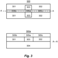
- Figure 3 is a schematic diagram illustrating the waveguide from Figure 2 in more detail, according to examples.
- Figure 300 illustrates a plan view of parts of the structure and
- Figure 300a illustrates a longitudinal cross section of the structure corresponding with line A---A in Figure 300.
- the waveguide 305 has a first portion of the waveguide 305a, a second portion of the waveguide 305b and a third portion of the waveguide 305c.
- the first portion 305a, second portion 305b and third portion 305c have substantially the same thickness such that the upper surface of the waveguide 305 has a planar surface.
- the first portion 305a, second portion 305b and third portion 305c are located along a longitudinal axis of the waveguide where the first portion 305a is at a first point of the longitudinal axis, the second portion 305b is at a second point of the longitudinal axis and the third portion 305c is at a third point of the longitudinal axis.
- the first portion of the waveguide 305a is on and in contact with a surface area of the element.
- the first portion of the waveguide 305a does not overlap the first portion 301 or second portion 302 or indeed any of the first layer of the n-type semiconductor material.
- the second portion of the waveguide 305b is on a surface area of the first portion 301 of the first layer of the n-type semiconductor material.
- the surface area of the first portion 301 of the first layer does not overlap the element 303.
- the third portion of the waveguide 305c is on a surface area of the second portion 302 of the first layer of n-type semiconductor material.
- the surface area of the second portion 302 of the first layer does not overlap the element 303.
- the waveguide 305 along a transverse axis of the structure, parallel with the surface of the substrate 304 and perpendicular to a longitudinal axis of the waveguide, has a width which, in examples, is less than the length of the waveguide 305 along the longitudinal axis of the waveguide, and is equal to or less than a width of the element.
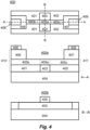
- Figure 4 is a schematic diagram illustrating the structure for a photonic integrated circuit from Figure 2 with PIC components, according to examples.
- Figure 400 illustrates a plan view of parts of the structure.
- Figure 400a illustrates a longitudinal cross section of the structure corresponding with line A---A in Figure 400 and
- Figure 400b illustrates a transverse cross section of the structure corresponding with line B-B in Figure 400.
- the structure comprises a first portion 406 and a second portion 407 of p-type semiconductor material.
- the first portion of the p-type semiconductor material 406 is deposited on part of the second portion of the waveguide 405b and the second portion 407 of the p-type semiconductor material is deposited on part of the third portion of the waveguide 405c.
- the first portion of the p-type semiconductor material 406 is deposited on part of the first portion of the first layer of n-type semiconductor material 401 and the second portion of the p-type semiconductor material 407 is deposited on part of the second portion of the first layer of n-type semiconductor material 402.
- the p-type semiconductor material comprises semiconductor material which is doped with acceptor impurities such that there is an abundance of holes, increasing the conductivity of the semiconductor material relative to the intrinsic semiconductor material or semiconductor material prior to doping.
- the majority of charge carriers in the p-type semiconductor material are positive holes.
- the p-type semiconductor material may be highly doped with acceptor impurities, where the dopant comprises a significant percentage of the chemical constituents of the semiconductor material.
- the p-type semiconductor material is for example of doped InP, InGaAsP, InAlGaAs, InGaAs, or InAlAs.
- a first electrical contact layer 408 is deposited on the first portion p-type semiconductor material 406.
- a second electrical contact layer 409 is deposited on the second portion of p-type semiconductor material 406.
- the first electrical contact layer 408 and second electrical contact layer 409 are composed of a metal material.
- the electrical contact layers allow a voltage to be applied across each PIN structure.
- the contact layer for the p-type semiconductor material is for example a combination of titanium (Ti), platinum (Pt) or Chromium (Cr) and Gold (Au).
- Such an absence of p-type material can also help reduce flow of electrical current between PIC components, especially if the element described herein is used to reduce electrical current flow in the n-type semiconductor layer.
- a PIC component is any component, electrical or optical which can be used to form a PIC.
- PIC components include waveguides, multimode interferometers (MMIs), P-N junctions, a semiconductor optical amplifier (SOA), an electro-absorption modulator (EAM) or an electro-optic phase modulator (EOPM).
- MMIs can be used to split light into its constituent eigenmodes.
- P-N junctions comprise p-type and n-type semiconductor material and are used to construct many PIC components such as photodetectors.
- the PIN structure of the first PIC component 410 and first electrical contact layer 408 are together a first photodiode.
- a photodiode is a photodetector which can convert optical signals into electrical signals. The photodetector allows for electrical readout of signals that can be carried by the light confined in the waveguide.
- the PIN structure of the second PIC component 411 and second electrical contact layer 409 are together a second photodiode.
- the first portion of the waveguide 405a is located between, when taken along the longitudinal axis of the waveguide, the first PIC component and second PIC component.
- the first PIC component 410 and second PIC component 411 are optically connected by the waveguide 405.
- Optically connected typically means that light confined by the waveguide 405 is able to travel between the first PIC and second PIC component without significant loss in energy. Without significant loss of energy typically means that no energy is lost however, a negligible amount of energy may be lost within acceptable tolerances.
- the material of the element 403 is configured to restrict, prevent or oppose the flow of current between the first PIC component 410 and second PIC component 411, such that there is an observable reduction or prevention of electrical current flowing between the first PIC component 410 and second PIC component 411 compared to the current flowing between the two PIC components if the element 403 was instead of the n-type semiconductor material. Note that even in the case of entirely preventing the current flow, it is appreciated that a negligible current may still flow between the two PIC components.
- the element 403 is, when taken along the longitudinal axis, between the first PIC 410 and second PIC component 411.
- the element 403 is configured such that it has an increased electrical resistance relative to the n-type semiconductor material of the first portion 401 and second portion 402 of the first layer.
- a current might still be able to flow to some degree between the first and second PIC components via the first portion of the first layer of n-type semiconductor material 401 through the second element 403 to the second portion of the first layer of n-type semiconductor material 402.
- a current can also flow between the first and second PIC components via the waveguide 405 material(s).
- the greater electrical resistance of the element 403 may however restrict the flow of the current to the waveguide 405, in turn decreasing the cross-sectional amount (e.g. along B---B) of electrically conductive material through which the electrical current can flow.
- Figure 5 is a schematic diagram illustrating a structure for a PIC comprising a balanced photodetector, according to examples.
- the diagram illustrates a plan view of at least part of the structure.
- the structure is a structure of semiconductor materials.
- the structure comprises a first PIC component 510 and a first waveguide 505a optically connecting the first PIC component to a second PIC component 514.
- the second PIC component 514 is optically connected to a third PIC component 516 by a second waveguide 505b.
- the first waveguide 505a and second waveguide are for example composed of an identical material composition 502b within acceptable tolerances.
- the structure comprises a substrate with a first layer of n-type semiconductor material thereon.
- the n-type semiconductor material has a first electrical resistance.
- the structure also comprises a first element 503a and a second element 503b.
- the structure instead of the first and second elements, the structure instead comprises a third element 503c deposited on the upper surface area of the substrate.
- An element refers to a block, volume, region or layer of the semi-insulating material described above, dimensioned appropriately to reduce electrical current flow between respective first and second portions of the first layer on either side of each block.
- the plurality of n-type semiconductor material portions 501, 502 and the first element 503a, second element 503b and third element 503b do not overlap each other.
- the material of the element has a second electrical resistance.
- the first electrical resistance is less than the second electrical resistance such that the respective elements are each configured to reduce electric current flow, similar in function to an electrical resistor for example, as each element has a greater electrical resistance than the electrical resistance of the n-type semiconductor material.
- Such an element reduces flow of electrical current from one side of the element to the other, for example by restricting, preventing or opposing the flow of electrical current.
- the plurality of portions of the first layer of n-type semiconductor material 501, 502 and the first element 503a, second element 503b and third element 508 together provide a substantially planar upper surface.
- the first waveguide 505a and second waveguide 505b are deposited on the first layer of n-type semiconductor and also on respective elements.
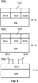
- Figure 6 is a schematic diagram illustrating aspects of the balanced photodetector of Figure 5 in more detail, according to examples.
- Figure 500a illustrates a cross section of the structure at a longitudinal axis corresponding with line A---A in Figure 500, for the first waveguide 505a.
- the first element 503a is deposited between and abuts each of a first portion 501a of the n-type semiconductor material and a second portion 502a of the n-type semiconductor material.
- the first element 503a is located at a first point on the longitudinal axis of the first waveguide 505a and is overlapped by and in contact with a first portion of the first waveguide 505a.
- Figure 500b illustrates a cross section of the structure at a longitudinal axis corresponding with line B---B in Figure 500, for the second waveguide 505b.
- the second element 503b is deposited between and abuts each of a third portion 501b of the n-type semiconductor material and a fourth portion 502b of the n-type semiconductor material.
- the second element 503b is located at a first point on the longitudinal axis of the second waveguide 505b and is overlapped by a first portion of the second waveguide 505b.
- a second portion of the second waveguide 505b overlaps the third portion of the first layer of n-type semiconductor material 501b.
- a third portion of the second waveguide 505b overlaps the fourth portion of the first layer of n-type semiconductor material 502b.
- the second PIC component 514 is a multimode interferometer (MMI).
- MMI multimode interferometer
- the MMI the light is confined by a single waveguide. After the MMI, the light reaches a junction where the single waveguide splits into the first waveguide 505a and second waveguide 505b.
- Figure 500c illustrates a cross section of the structure at a transverse axis corresponding with line C---C in Figure 500, for the waveguide junction 518 where the waveguide splits into the first waveguide 505a and second waveguide 505b.
- the third element 503c is deposited between and abuts a fifth portion 501c of the n-type semiconductor material and a sixth portion 502c of the n-type semiconductor material.
- the third element 503c is located between first and second PIC components on one side, and on the other side the waveguide junction 518 which is optically connected to the first waveguide 505a and second waveguide 505b.
- the term between at least in this example is used with reference to components on the longitudinal axis of the respective waveguide, taking into account any bend or other non-straight line shape of the waveguide.
- a portion of the first waveguide 505a is deposited on a first part of the third element 503c.
- a portion of the second waveguide 505b is deposited on a second part of the third element 503c.
- the first and second parts of the third element 503c do not overlap.
- the first PIC component 510 is comprised of part of the first layer of n-type semiconductor material, part of the first waveguide 505a, a first portion of p-type semiconductor material deposited on a portion of the first waveguide 505a and an electrical contact layer deposited on a portion of the first portion of p-type semiconductor material.
- the third PIC component 516 is comprised of part of the first layer of n-type semiconductor material, part of the second waveguide 505b, a second portion of p-type semiconductor material deposited on a portion of the second waveguide 505a and an electrical contact layer deposited on a portion of the first portion of p-type semiconductor material.
- the first PIC component 510 and third PIC component 516 are photodiodes and are configured in combination with the MMI 503 to operate as a balanced photodetector.
- each element acts to reduce, by for example restricting, preventing, or opposing the flow of electric current between the first photodiode 510 and second photodiode 516. Hence, electrical cross-talk between the photodiodes can be reduced.
- Such techniques may include chemical vapour deposition techniques such as metalorganic vapour-phase epitaxy (MOVPE) or molecular beam epitaxy (MBE). Etching techniques may be used to remove portions of material, as part of patterning, as the skilled person will appreciate.
- CVPE metalorganic vapour-phase epitaxy
- MBE molecular beam epitaxy
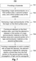
- a structure in accordance with examples described above is manufactured by a method comprising: providing a substrate; depositing n-type semiconductor on the first surface area, the second surface area, and the third surface area of the substrate; removing n-type semiconductor of the first layer on the third surface area; forming the element on the third surface area, such that the element is between the first portion of n-type semiconductor material on the first surface area and the second portion of n-type semiconductor material on the second surface area; and forming a waveguide on and in contact with at least the element, the element comprising a material for reducing electric current flow from the first portion to the second portion during propagation of light via the waveguide.
- the structure is manufactured by a method comprising: providing the substrate; removing a first portion of the substrate to form the first surface area of the substrate, and removing a second portion of the substrate to form the second surface area of the substrate, to leave an unremoved portion of the substrate between the first surface area and the second surface area, the unremoved portion corresponding to the third surface area of the substrate; depositing n-type semiconductor on the first surface area and the second surface area; forming the waveguide on and in contact with at least the unremoved portion, the unremoved portion being the element between the first portion of n-type semiconductor material and the second portion of n-type semiconductor material, the element comprising a material for reducing electric current flow from the first portion of n-type semiconductor material to the second portion of n-type semiconductor material during propagation of light via the waveguide.
- the method in examples comprises: forming the first PIC component (such as a photodiode); forming the second PIC component (such as a MMI) optically connected to the first PIC component by the waveguide, with the element dimensioned and of a material with an electrical resistivity such that the element at least one of reduces, prevents or opposes electric current flow between the first PIC component and the second PIC component.
- the first PIC component such as a photodiode
- the second PIC component such as a MMI
Landscapes
- Physics & Mathematics (AREA)
- General Physics & Mathematics (AREA)
- Optics & Photonics (AREA)
- Engineering & Computer Science (AREA)
- Microelectronics & Electronic Packaging (AREA)
- Optical Integrated Circuits (AREA)
- Light Receiving Elements (AREA)
Applications Claiming Priority (2)
| Application Number | Priority Date | Filing Date | Title |
|---|---|---|---|
| GB2001404.9A GB2592906B (en) | 2020-01-31 | 2020-01-31 | Structure for a photonic integrated circuit |
| PCT/EP2021/052198 WO2021152143A1 (en) | 2020-01-31 | 2021-01-29 | Structure for a photonic integrated circuit |
Publications (2)
| Publication Number | Publication Date |
|---|---|
| EP4097517A1 EP4097517A1 (en) | 2022-12-07 |
| EP4097517B1 true EP4097517B1 (en) | 2024-03-06 |
Family
ID=69800066
Family Applications (1)
| Application Number | Title | Priority Date | Filing Date |
|---|---|---|---|
| EP21706845.1A Active EP4097517B1 (en) | 2020-01-31 | 2021-01-29 | Structure for a photonic integrated circuit |
Country Status (6)
| Country | Link |
|---|---|
| US (1) | US12546936B2 (cg-RX-API-DMAC7.html) |
| EP (1) | EP4097517B1 (cg-RX-API-DMAC7.html) |
| JP (1) | JP2023512931A (cg-RX-API-DMAC7.html) |
| CN (1) | CN115053159A (cg-RX-API-DMAC7.html) |
| GB (1) | GB2592906B (cg-RX-API-DMAC7.html) |
| WO (1) | WO2021152143A1 (cg-RX-API-DMAC7.html) |
Families Citing this family (2)
| Publication number | Priority date | Publication date | Assignee | Title |
|---|---|---|---|---|
| GB202212686D0 (en) * | 2022-08-31 | 2022-10-12 | Smart Photonics Holding B V | Method of providing a wafer |
| GB2638384A (en) * | 2024-01-12 | 2025-08-27 | Smart Photonics Holding B V | Part of photonic integrated circuit and method of manufacturing same |
Family Cites Families (10)
| Publication number | Priority date | Publication date | Assignee | Title |
|---|---|---|---|---|
| JP2003264334A (ja) * | 2002-03-08 | 2003-09-19 | Hitachi Ltd | 半導体レーザ素子及び半導体レーザモジュール |
| US6771682B2 (en) * | 2002-08-12 | 2004-08-03 | Infinera Corporation | Electrical isolation of optical components in photonic integrated circuits (PICs) |
| US20100310256A1 (en) * | 2007-02-27 | 2010-12-09 | Celight, Inc. | Parallel optical receiver for optical systems |
| JP5260909B2 (ja) * | 2007-07-23 | 2013-08-14 | 住友電気工業株式会社 | 受光デバイス |
| US8269297B2 (en) * | 2009-12-23 | 2012-09-18 | Infinera Corporation | Photodiode isolation in a photonic integrated circuit |
| US8948227B2 (en) * | 2013-01-11 | 2015-02-03 | Source Photonics, Inc. | Isolated modulator electrodes for low power consumption |
| JP6213222B2 (ja) * | 2013-12-24 | 2017-10-18 | 富士通株式会社 | 光半導体装置及びその製造方法 |
| CN108351467B (zh) * | 2015-07-22 | 2020-10-30 | Bb光电公司 | 具有介质波导的化合物半导体光子集成电路 |
| KR20180085221A (ko) * | 2017-01-18 | 2018-07-26 | 엘지이노텍 주식회사 | 반도체 소자 및 이를 포함하는 광 모듈 |
| CN113176676B (zh) * | 2021-04-16 | 2022-11-15 | 上海曦智科技有限公司 | 光学调制器和光学集成系统 |
-
2020
- 2020-01-31 GB GB2001404.9A patent/GB2592906B/en active Active
-
2021
- 2021-01-29 WO PCT/EP2021/052198 patent/WO2021152143A1/en not_active Ceased
- 2021-01-29 JP JP2022543627A patent/JP2023512931A/ja active Pending
- 2021-01-29 EP EP21706845.1A patent/EP4097517B1/en active Active
- 2021-01-29 CN CN202180011378.XA patent/CN115053159A/zh active Pending
-
2022
- 2022-07-29 US US17/876,609 patent/US12546936B2/en active Active
Also Published As
| Publication number | Publication date |
|---|---|
| GB202001404D0 (en) | 2020-03-18 |
| GB2592906A (en) | 2021-09-15 |
| CN115053159A (zh) | 2022-09-13 |
| US12546936B2 (en) | 2026-02-10 |
| WO2021152143A1 (en) | 2021-08-05 |
| EP4097517A1 (en) | 2022-12-07 |
| US20220365276A1 (en) | 2022-11-17 |
| GB2592906B (en) | 2024-01-10 |
| JP2023512931A (ja) | 2023-03-30 |
Similar Documents
| Publication | Publication Date | Title |
|---|---|---|
| US8068526B2 (en) | Semiconductor optical device | |
| US7875943B2 (en) | Semiconductor photoreceptor device | |
| US12546936B2 (en) | Structure for a photonic integrated circuit | |
| US9696496B2 (en) | Semiconductor optical device and semiconductor assembly | |
| US8847357B2 (en) | Opto-electronic device | |
| JP7302775B2 (ja) | 半導体受光素子 | |
| EP0252565B1 (fr) | Dispositif semiconducteur intégré du type dispositif de couplage entre un photodéecteur et un guide d'ond lumineuse | |
| US12044569B2 (en) | Light receiving device and light receiving apparatus | |
| JP4109159B2 (ja) | 半導体受光素子 | |
| Wang et al. | High-speed InGaAs PIN photodetector with planar buried heterostructure | |
| Chandrasekhar et al. | Integrated directional couplers with photodetectors by hydride vapour phase epitaxy | |
| Wang et al. | An 850 nm InGaAs Modified Uni-Traveling-Carrier Photodiode Enhanced by Distributed Bragg Reflector | |
| TAKEUCHI et al. | A high-efficiency waveguide photodiode for 40-Gb/s optical receivers | |
| US12588299B2 (en) | Semiconductor light reception element | |
| US20220254940A1 (en) | Light-receiving device and method of manufacturing light-receiving device | |
| JP6491612B2 (ja) | 半導体光集積素子 | |
| Cavailles et al. | Integration of detectors with GaInAsP/InP carrier depletion optical switches | |
| Forcade et al. | Improved NPIN Junctions for 100 GHz InP Mach-Zehnder Modulators | |
| KR101001832B1 (ko) | 전류차단층을 구비하는 수광소자 어레이 및 그의 제조방법 | |
| Royter et al. | Integrated packaging of uni-traveling-carrier photodiodes on sapphire substrate by wafer bonding | |
| Nakaji et al. | The balanced photodetector buried with semi-insulating InP | |
| Seto et al. | Comparative study of | |
| JPH0992872A (ja) | 導波路型半導体受光器 | |
| JPH08111564A (ja) | 半導体素子とその製造方法 | |
| JPH02228077A (ja) | 半導体受光素子 |
Legal Events
| Date | Code | Title | Description |
|---|---|---|---|
| STAA | Information on the status of an ep patent application or granted ep patent |
Free format text: STATUS: UNKNOWN |
|
| STAA | Information on the status of an ep patent application or granted ep patent |
Free format text: STATUS: THE INTERNATIONAL PUBLICATION HAS BEEN MADE |
|
| PUAI | Public reference made under article 153(3) epc to a published international application that has entered the european phase |
Free format text: ORIGINAL CODE: 0009012 |
|
| STAA | Information on the status of an ep patent application or granted ep patent |
Free format text: STATUS: REQUEST FOR EXAMINATION WAS MADE |
|
| 17P | Request for examination filed |
Effective date: 20220831 |
|
| AK | Designated contracting states |
Kind code of ref document: A1 Designated state(s): AL AT BE BG CH CY CZ DE DK EE ES FI FR GB GR HR HU IE IS IT LI LT LU LV MC MK MT NL NO PL PT RO RS SE SI SK SM TR |
|
| DAV | Request for validation of the european patent (deleted) | ||
| DAX | Request for extension of the european patent (deleted) | ||
| GRAP | Despatch of communication of intention to grant a patent |
Free format text: ORIGINAL CODE: EPIDOSNIGR1 |
|
| STAA | Information on the status of an ep patent application or granted ep patent |
Free format text: STATUS: GRANT OF PATENT IS INTENDED |
|
| INTG | Intention to grant announced |
Effective date: 20230912 |
|
| P01 | Opt-out of the competence of the unified patent court (upc) registered |
Effective date: 20231205 |
|
| GRAS | Grant fee paid |
Free format text: ORIGINAL CODE: EPIDOSNIGR3 |
|
| GRAA | (expected) grant |
Free format text: ORIGINAL CODE: 0009210 |
|
| STAA | Information on the status of an ep patent application or granted ep patent |
Free format text: STATUS: THE PATENT HAS BEEN GRANTED |
|
| RAP3 | Party data changed (applicant data changed or rights of an application transferred) |
Owner name: SMART PHOTONICS HOLDING B.V. |
|
| AK | Designated contracting states |
Kind code of ref document: B1 Designated state(s): AL AT BE BG CH CY CZ DE DK EE ES FI FR GB GR HR HU IE IS IT LI LT LU LV MC MK MT NL NO PL PT RO RS SE SI SK SM TR |
|
| REG | Reference to a national code |
Ref country code: CH Ref legal event code: EP |
|
| REG | Reference to a national code |
Ref country code: IE Ref legal event code: FG4D |
|
| REG | Reference to a national code |
Ref country code: DE Ref legal event code: R096 Ref document number: 602021010128 Country of ref document: DE |
|
| REG | Reference to a national code |
Ref country code: NL Ref legal event code: FP |
|
| REG | Reference to a national code |
Ref country code: LT Ref legal event code: MG9D |
|
| PG25 | Lapsed in a contracting state [announced via postgrant information from national office to epo] |
Ref country code: LT Free format text: LAPSE BECAUSE OF FAILURE TO SUBMIT A TRANSLATION OF THE DESCRIPTION OR TO PAY THE FEE WITHIN THE PRESCRIBED TIME-LIMIT Effective date: 20240306 |
|
| PG25 | Lapsed in a contracting state [announced via postgrant information from national office to epo] |
Ref country code: GR Free format text: LAPSE BECAUSE OF FAILURE TO SUBMIT A TRANSLATION OF THE DESCRIPTION OR TO PAY THE FEE WITHIN THE PRESCRIBED TIME-LIMIT Effective date: 20240607 |
|
| PG25 | Lapsed in a contracting state [announced via postgrant information from national office to epo] |
Ref country code: RS Free format text: LAPSE BECAUSE OF FAILURE TO SUBMIT A TRANSLATION OF THE DESCRIPTION OR TO PAY THE FEE WITHIN THE PRESCRIBED TIME-LIMIT Effective date: 20240606 Ref country code: HR Free format text: LAPSE BECAUSE OF FAILURE TO SUBMIT A TRANSLATION OF THE DESCRIPTION OR TO PAY THE FEE WITHIN THE PRESCRIBED TIME-LIMIT Effective date: 20240306 |
|
| PG25 | Lapsed in a contracting state [announced via postgrant information from national office to epo] |
Ref country code: ES Free format text: LAPSE BECAUSE OF FAILURE TO SUBMIT A TRANSLATION OF THE DESCRIPTION OR TO PAY THE FEE WITHIN THE PRESCRIBED TIME-LIMIT Effective date: 20240306 |
|
| PG25 | Lapsed in a contracting state [announced via postgrant information from national office to epo] |
Ref country code: RS Free format text: LAPSE BECAUSE OF FAILURE TO SUBMIT A TRANSLATION OF THE DESCRIPTION OR TO PAY THE FEE WITHIN THE PRESCRIBED TIME-LIMIT Effective date: 20240606 Ref country code: NO Free format text: LAPSE BECAUSE OF FAILURE TO SUBMIT A TRANSLATION OF THE DESCRIPTION OR TO PAY THE FEE WITHIN THE PRESCRIBED TIME-LIMIT Effective date: 20240606 Ref country code: LT Free format text: LAPSE BECAUSE OF FAILURE TO SUBMIT A TRANSLATION OF THE DESCRIPTION OR TO PAY THE FEE WITHIN THE PRESCRIBED TIME-LIMIT Effective date: 20240306 Ref country code: HR Free format text: LAPSE BECAUSE OF FAILURE TO SUBMIT A TRANSLATION OF THE DESCRIPTION OR TO PAY THE FEE WITHIN THE PRESCRIBED TIME-LIMIT Effective date: 20240306 Ref country code: GR Free format text: LAPSE BECAUSE OF FAILURE TO SUBMIT A TRANSLATION OF THE DESCRIPTION OR TO PAY THE FEE WITHIN THE PRESCRIBED TIME-LIMIT Effective date: 20240607 Ref country code: FI Free format text: LAPSE BECAUSE OF FAILURE TO SUBMIT A TRANSLATION OF THE DESCRIPTION OR TO PAY THE FEE WITHIN THE PRESCRIBED TIME-LIMIT Effective date: 20240306 Ref country code: ES Free format text: LAPSE BECAUSE OF FAILURE TO SUBMIT A TRANSLATION OF THE DESCRIPTION OR TO PAY THE FEE WITHIN THE PRESCRIBED TIME-LIMIT Effective date: 20240306 Ref country code: BG Free format text: LAPSE BECAUSE OF FAILURE TO SUBMIT A TRANSLATION OF THE DESCRIPTION OR TO PAY THE FEE WITHIN THE PRESCRIBED TIME-LIMIT Effective date: 20240306 |
|
| REG | Reference to a national code |
Ref country code: AT Ref legal event code: MK05 Ref document number: 1664081 Country of ref document: AT Kind code of ref document: T Effective date: 20240306 |
|
| PG25 | Lapsed in a contracting state [announced via postgrant information from national office to epo] |
Ref country code: SE Free format text: LAPSE BECAUSE OF FAILURE TO SUBMIT A TRANSLATION OF THE DESCRIPTION OR TO PAY THE FEE WITHIN THE PRESCRIBED TIME-LIMIT Effective date: 20240306 Ref country code: LV Free format text: LAPSE BECAUSE OF FAILURE TO SUBMIT A TRANSLATION OF THE DESCRIPTION OR TO PAY THE FEE WITHIN THE PRESCRIBED TIME-LIMIT Effective date: 20240306 |
|
| PG25 | Lapsed in a contracting state [announced via postgrant information from national office to epo] |
Ref country code: IS Free format text: LAPSE BECAUSE OF FAILURE TO SUBMIT A TRANSLATION OF THE DESCRIPTION OR TO PAY THE FEE WITHIN THE PRESCRIBED TIME-LIMIT Effective date: 20240706 |
|
| PG25 | Lapsed in a contracting state [announced via postgrant information from national office to epo] |
Ref country code: PT Free format text: LAPSE BECAUSE OF FAILURE TO SUBMIT A TRANSLATION OF THE DESCRIPTION OR TO PAY THE FEE WITHIN THE PRESCRIBED TIME-LIMIT Effective date: 20240708 Ref country code: SM Free format text: LAPSE BECAUSE OF FAILURE TO SUBMIT A TRANSLATION OF THE DESCRIPTION OR TO PAY THE FEE WITHIN THE PRESCRIBED TIME-LIMIT Effective date: 20240306 |
|
| PG25 | Lapsed in a contracting state [announced via postgrant information from national office to epo] |
Ref country code: EE Free format text: LAPSE BECAUSE OF FAILURE TO SUBMIT A TRANSLATION OF THE DESCRIPTION OR TO PAY THE FEE WITHIN THE PRESCRIBED TIME-LIMIT Effective date: 20240306 Ref country code: CZ Free format text: LAPSE BECAUSE OF FAILURE TO SUBMIT A TRANSLATION OF THE DESCRIPTION OR TO PAY THE FEE WITHIN THE PRESCRIBED TIME-LIMIT Effective date: 20240306 |
|
| PG25 | Lapsed in a contracting state [announced via postgrant information from national office to epo] |
Ref country code: AT Free format text: LAPSE BECAUSE OF FAILURE TO SUBMIT A TRANSLATION OF THE DESCRIPTION OR TO PAY THE FEE WITHIN THE PRESCRIBED TIME-LIMIT Effective date: 20240306 |
|
| PG25 | Lapsed in a contracting state [announced via postgrant information from national office to epo] |
Ref country code: PL Free format text: LAPSE BECAUSE OF FAILURE TO SUBMIT A TRANSLATION OF THE DESCRIPTION OR TO PAY THE FEE WITHIN THE PRESCRIBED TIME-LIMIT Effective date: 20240306 |
|
| PG25 | Lapsed in a contracting state [announced via postgrant information from national office to epo] |
Ref country code: SK Free format text: LAPSE BECAUSE OF FAILURE TO SUBMIT A TRANSLATION OF THE DESCRIPTION OR TO PAY THE FEE WITHIN THE PRESCRIBED TIME-LIMIT Effective date: 20240306 |
|
| PG25 | Lapsed in a contracting state [announced via postgrant information from national office to epo] |
Ref country code: SM Free format text: LAPSE BECAUSE OF FAILURE TO SUBMIT A TRANSLATION OF THE DESCRIPTION OR TO PAY THE FEE WITHIN THE PRESCRIBED TIME-LIMIT Effective date: 20240306 Ref country code: SK Free format text: LAPSE BECAUSE OF FAILURE TO SUBMIT A TRANSLATION OF THE DESCRIPTION OR TO PAY THE FEE WITHIN THE PRESCRIBED TIME-LIMIT Effective date: 20240306 Ref country code: RO Free format text: LAPSE BECAUSE OF FAILURE TO SUBMIT A TRANSLATION OF THE DESCRIPTION OR TO PAY THE FEE WITHIN THE PRESCRIBED TIME-LIMIT Effective date: 20240306 Ref country code: PT Free format text: LAPSE BECAUSE OF FAILURE TO SUBMIT A TRANSLATION OF THE DESCRIPTION OR TO PAY THE FEE WITHIN THE PRESCRIBED TIME-LIMIT Effective date: 20240708 Ref country code: PL Free format text: LAPSE BECAUSE OF FAILURE TO SUBMIT A TRANSLATION OF THE DESCRIPTION OR TO PAY THE FEE WITHIN THE PRESCRIBED TIME-LIMIT Effective date: 20240306 Ref country code: IS Free format text: LAPSE BECAUSE OF FAILURE TO SUBMIT A TRANSLATION OF THE DESCRIPTION OR TO PAY THE FEE WITHIN THE PRESCRIBED TIME-LIMIT Effective date: 20240706 Ref country code: EE Free format text: LAPSE BECAUSE OF FAILURE TO SUBMIT A TRANSLATION OF THE DESCRIPTION OR TO PAY THE FEE WITHIN THE PRESCRIBED TIME-LIMIT Effective date: 20240306 Ref country code: CZ Free format text: LAPSE BECAUSE OF FAILURE TO SUBMIT A TRANSLATION OF THE DESCRIPTION OR TO PAY THE FEE WITHIN THE PRESCRIBED TIME-LIMIT Effective date: 20240306 Ref country code: AT Free format text: LAPSE BECAUSE OF FAILURE TO SUBMIT A TRANSLATION OF THE DESCRIPTION OR TO PAY THE FEE WITHIN THE PRESCRIBED TIME-LIMIT Effective date: 20240306 |
|
| PG25 | Lapsed in a contracting state [announced via postgrant information from national office to epo] |
Ref country code: IT Free format text: LAPSE BECAUSE OF FAILURE TO SUBMIT A TRANSLATION OF THE DESCRIPTION OR TO PAY THE FEE WITHIN THE PRESCRIBED TIME-LIMIT Effective date: 20240306 |
|
| REG | Reference to a national code |
Ref country code: DE Ref legal event code: R097 Ref document number: 602021010128 Country of ref document: DE |
|
| PG25 | Lapsed in a contracting state [announced via postgrant information from national office to epo] |
Ref country code: IT Free format text: LAPSE BECAUSE OF FAILURE TO SUBMIT A TRANSLATION OF THE DESCRIPTION OR TO PAY THE FEE WITHIN THE PRESCRIBED TIME-LIMIT Effective date: 20240306 |
|
| PLBE | No opposition filed within time limit |
Free format text: ORIGINAL CODE: 0009261 |
|
| STAA | Information on the status of an ep patent application or granted ep patent |
Free format text: STATUS: NO OPPOSITION FILED WITHIN TIME LIMIT |
|
| PG25 | Lapsed in a contracting state [announced via postgrant information from national office to epo] |
Ref country code: DK Free format text: LAPSE BECAUSE OF FAILURE TO SUBMIT A TRANSLATION OF THE DESCRIPTION OR TO PAY THE FEE WITHIN THE PRESCRIBED TIME-LIMIT Effective date: 20240306 |
|
| PG25 | Lapsed in a contracting state [announced via postgrant information from national office to epo] |
Ref country code: DK Free format text: LAPSE BECAUSE OF FAILURE TO SUBMIT A TRANSLATION OF THE DESCRIPTION OR TO PAY THE FEE WITHIN THE PRESCRIBED TIME-LIMIT Effective date: 20240306 |
|
| 26N | No opposition filed |
Effective date: 20241209 |
|
| PG25 | Lapsed in a contracting state [announced via postgrant information from national office to epo] |
Ref country code: SI Free format text: LAPSE BECAUSE OF FAILURE TO SUBMIT A TRANSLATION OF THE DESCRIPTION OR TO PAY THE FEE WITHIN THE PRESCRIBED TIME-LIMIT Effective date: 20240306 |
|
| REG | Reference to a national code |
Ref country code: CH Ref legal event code: PL |
|
| PG25 | Lapsed in a contracting state [announced via postgrant information from national office to epo] |
Ref country code: LU Free format text: LAPSE BECAUSE OF NON-PAYMENT OF DUE FEES Effective date: 20250129 Ref country code: MC Free format text: LAPSE BECAUSE OF FAILURE TO SUBMIT A TRANSLATION OF THE DESCRIPTION OR TO PAY THE FEE WITHIN THE PRESCRIBED TIME-LIMIT Effective date: 20240306 |
|
| PG25 | Lapsed in a contracting state [announced via postgrant information from national office to epo] |
Ref country code: CH Free format text: LAPSE BECAUSE OF NON-PAYMENT OF DUE FEES Effective date: 20250131 |
|
| PG25 | Lapsed in a contracting state [announced via postgrant information from national office to epo] |
Ref country code: IE Free format text: LAPSE BECAUSE OF NON-PAYMENT OF DUE FEES Effective date: 20250129 |
|
| PGFP | Annual fee paid to national office [announced via postgrant information from national office to epo] |
Ref country code: NL Payment date: 20260122 Year of fee payment: 6 |
|
| PGFP | Annual fee paid to national office [announced via postgrant information from national office to epo] |
Ref country code: GB Payment date: 20260126 Year of fee payment: 6 |
|
| PGFP | Annual fee paid to national office [announced via postgrant information from national office to epo] |
Ref country code: DE Payment date: 20260127 Year of fee payment: 6 |
|
| PGFP | Annual fee paid to national office [announced via postgrant information from national office to epo] |
Ref country code: BE Payment date: 20260123 Year of fee payment: 6 |
|
| PGFP | Annual fee paid to national office [announced via postgrant information from national office to epo] |
Ref country code: FR Payment date: 20260126 Year of fee payment: 6 |