EP4084084A1 - Zelluläre struktur von igbt mit umgekehrter leitung und igbt mit umgekehrter leitung - Google Patents
Zelluläre struktur von igbt mit umgekehrter leitung und igbt mit umgekehrter leitung Download PDFInfo
- Publication number
- EP4084084A1 EP4084084A1 EP20907435.0A EP20907435A EP4084084A1 EP 4084084 A1 EP4084084 A1 EP 4084084A1 EP 20907435 A EP20907435 A EP 20907435A EP 4084084 A1 EP4084084 A1 EP 4084084A1
- Authority
- EP
- European Patent Office
- Prior art keywords
- conductivity type
- type source
- region
- cellular structure
- source regions
- Prior art date
- Legal status (The legal status is an assumption and is not a legal conclusion. Google has not performed a legal analysis and makes no representation as to the accuracy of the status listed.)
- Pending
Links
Images


Classifications
-
- H—ELECTRICITY
- H10—SEMICONDUCTOR DEVICES; ELECTRIC SOLID-STATE DEVICES NOT OTHERWISE PROVIDED FOR
- H10D—INORGANIC ELECTRIC SEMICONDUCTOR DEVICES
- H10D12/00—Bipolar devices controlled by the field effect, e.g. insulated-gate bipolar transistors [IGBT]
- H10D12/411—Insulated-gate bipolar transistors [IGBT]
- H10D12/441—Vertical IGBTs
- H10D12/491—Vertical IGBTs having both emitter contacts and collector contacts in the same substrate side
-
- H—ELECTRICITY
- H10—SEMICONDUCTOR DEVICES; ELECTRIC SOLID-STATE DEVICES NOT OTHERWISE PROVIDED FOR
- H10D—INORGANIC ELECTRIC SEMICONDUCTOR DEVICES
- H10D62/00—Semiconductor bodies, or regions thereof, of devices having potential barriers
- H10D62/10—Shapes, relative sizes or dispositions of the regions of the semiconductor bodies; Shapes of the semiconductor bodies
- H10D62/17—Semiconductor regions connected to electrodes not carrying current to be rectified, amplified or switched, e.g. channel regions
- H10D62/393—Body regions of DMOS transistors or IGBTs
-
- H—ELECTRICITY
- H10—SEMICONDUCTOR DEVICES; ELECTRIC SOLID-STATE DEVICES NOT OTHERWISE PROVIDED FOR
- H10D—INORGANIC ELECTRIC SEMICONDUCTOR DEVICES
- H10D12/00—Bipolar devices controlled by the field effect, e.g. insulated-gate bipolar transistors [IGBT]
- H10D12/411—Insulated-gate bipolar transistors [IGBT]
- H10D12/441—Vertical IGBTs
- H10D12/461—Vertical IGBTs having non-planar surfaces, e.g. having trenches, recesses or pillars in the surfaces of the emitter, base or collector regions
- H10D12/481—Vertical IGBTs having non-planar surfaces, e.g. having trenches, recesses or pillars in the surfaces of the emitter, base or collector regions having gate structures on slanted surfaces, on vertical surfaces, or in grooves, e.g. trench gate IGBTs
-
- H—ELECTRICITY
- H10—SEMICONDUCTOR DEVICES; ELECTRIC SOLID-STATE DEVICES NOT OTHERWISE PROVIDED FOR
- H10D—INORGANIC ELECTRIC SEMICONDUCTOR DEVICES
- H10D62/00—Semiconductor bodies, or regions thereof, of devices having potential barriers
- H10D62/10—Shapes, relative sizes or dispositions of the regions of the semiconductor bodies; Shapes of the semiconductor bodies
- H10D62/124—Shapes, relative sizes or dispositions of the regions of semiconductor bodies or of junctions between the regions
- H10D62/126—Top-view geometrical layouts of the regions or the junctions
- H10D62/127—Top-view geometrical layouts of the regions or the junctions of cellular field-effect devices, e.g. multicellular DMOS transistors or IGBTs
-
- H—ELECTRICITY
- H10—SEMICONDUCTOR DEVICES; ELECTRIC SOLID-STATE DEVICES NOT OTHERWISE PROVIDED FOR
- H10D—INORGANIC ELECTRIC SEMICONDUCTOR DEVICES
- H10D62/00—Semiconductor bodies, or regions thereof, of devices having potential barriers
- H10D62/10—Shapes, relative sizes or dispositions of the regions of the semiconductor bodies; Shapes of the semiconductor bodies
- H10D62/13—Semiconductor regions connected to electrodes carrying current to be rectified, amplified or switched, e.g. source or drain regions
- H10D62/141—Anode or cathode regions of thyristors; Collector or emitter regions of gated bipolar-mode devices, e.g. of IGBTs
- H10D62/142—Anode regions of thyristors or collector regions of gated bipolar-mode devices
-
- H—ELECTRICITY
- H10—SEMICONDUCTOR DEVICES; ELECTRIC SOLID-STATE DEVICES NOT OTHERWISE PROVIDED FOR
- H10D—INORGANIC ELECTRIC SEMICONDUCTOR DEVICES
- H10D62/00—Semiconductor bodies, or regions thereof, of devices having potential barriers
- H10D62/10—Shapes, relative sizes or dispositions of the regions of the semiconductor bodies; Shapes of the semiconductor bodies
- H10D62/13—Semiconductor regions connected to electrodes carrying current to be rectified, amplified or switched, e.g. source or drain regions
- H10D62/141—Anode or cathode regions of thyristors; Collector or emitter regions of gated bipolar-mode devices, e.g. of IGBTs
- H10D62/145—Emitter regions of IGBTs
-
- H—ELECTRICITY
- H10—SEMICONDUCTOR DEVICES; ELECTRIC SOLID-STATE DEVICES NOT OTHERWISE PROVIDED FOR
- H10D—INORGANIC ELECTRIC SEMICONDUCTOR DEVICES
- H10D64/00—Electrodes of devices having potential barriers
- H10D64/01—Manufacture or treatment
-
- H—ELECTRICITY
- H10—SEMICONDUCTOR DEVICES; ELECTRIC SOLID-STATE DEVICES NOT OTHERWISE PROVIDED FOR
- H10D—INORGANIC ELECTRIC SEMICONDUCTOR DEVICES
- H10D64/00—Electrodes of devices having potential barriers
- H10D64/20—Electrodes characterised by their shapes, relative sizes or dispositions
- H10D64/23—Electrodes carrying the current to be rectified, amplified, oscillated or switched, e.g. sources, drains, anodes or cathodes
- H10D64/232—Emitter electrodes for IGBTs
-
- H—ELECTRICITY
- H10—SEMICONDUCTOR DEVICES; ELECTRIC SOLID-STATE DEVICES NOT OTHERWISE PROVIDED FOR
- H10D—INORGANIC ELECTRIC SEMICONDUCTOR DEVICES
- H10D64/00—Electrodes of devices having potential barriers
- H10D64/20—Electrodes characterised by their shapes, relative sizes or dispositions
- H10D64/23—Electrodes carrying the current to be rectified, amplified, oscillated or switched, e.g. sources, drains, anodes or cathodes
- H10D64/251—Source or drain electrodes for field-effect devices
- H10D64/252—Source or drain electrodes for field-effect devices for vertical or pseudo-vertical devices
-
- H—ELECTRICITY
- H10—SEMICONDUCTOR DEVICES; ELECTRIC SOLID-STATE DEVICES NOT OTHERWISE PROVIDED FOR
- H10D—INORGANIC ELECTRIC SEMICONDUCTOR DEVICES
- H10D12/00—Bipolar devices controlled by the field effect, e.g. insulated-gate bipolar transistors [IGBT]
- H10D12/411—Insulated-gate bipolar transistors [IGBT]
- H10D12/441—Vertical IGBTs
- H10D12/461—Vertical IGBTs having non-planar surfaces, e.g. having trenches, recesses or pillars in the surfaces of the emitter, base or collector regions
-
- H—ELECTRICITY
- H10—SEMICONDUCTOR DEVICES; ELECTRIC SOLID-STATE DEVICES NOT OTHERWISE PROVIDED FOR
- H10D—INORGANIC ELECTRIC SEMICONDUCTOR DEVICES
- H10D62/00—Semiconductor bodies, or regions thereof, of devices having potential barriers
- H10D62/60—Impurity distributions or concentrations
Definitions
- the disclosure relates to the technical field of semiconductor devices, and in particular to a cellular structure of a reverse conducting IGBT and a reverse conducting IGBT.
- An insulated gate bipolar transistor is a composite fully-controlled voltage-drive power semiconductor device formed by a bipolar junction transistor (BJT) and a metal-oxide-semiconductor field-effect transistor (MOSFET), and has become a kind of semiconductor device that is used most widely in large-voltage, large-current and highfrequency power electronic applications.
- IGBT In the application of the IGBT, it is usually necessary to connect a fast recovery diode (FRD) of a corresponding specification in antiparallel as a current bleeding circuit when the IGBT is turned off, so as to protect an IGBT chip.
- FRD fast recovery diode
- the IGBT and the FRD can be integrated in the same chip, i.e. a reverse conducting IGBT (RC-IGBT).
- a traditional cellular structure of a reverse conducting IGBT integrates functions of the IGBT device and the FRD device, and when the reverse conducting IGBT works in an FRD mode, a change in the gate voltage strongly affects the performance of the FRD.
- the gate voltage of the reverse conducting IGBT is less than or equal to 0 V, the reverse conducting IGBT does not form a reverse carrier channel, an anode of the FRD is not short-circuited, the anode injection efficiency of the FRD is high, and a forward turn-on voltage drop of the FRD is relatively low.
- a reverse carrier channel is formed between two source regions that have opposite conductivity types in the reverse conducting IGBT, which short circuits the anode of the FRD, causing the decrease of the anode injection efficiency of the FRD and the increase of the forward turn-on voltage drop of the FRD, such that the FRD cannot normally work.
- the disclosure provides a cellular structure of a reverse conducting IGBT and a reverse conducting IGBT.
- the disclosure provides a cellular structure of a reverse conducting IGBT, the cellular structure including:
- the surface of the second conductivity type source region is lower than the surface of the first conductivity type source regions by more than 0.3 ⁇ m.
- the conductive layer is a metal layer or a silicon alloy layer.
- the cellular structure further includes: a first conductivity type storage region arranged in the drift region and located below the well region.
- the doping concentration of the storage region is higher than the doping concentration of the substrate by one to two orders of magnitude.
- the cellular structure further includes: a lifetime control region arranged in the well region and located below the second conductivity type source region.
- the gate structure comprises a gate insulating layer located on the drift layer and in contact with surfaces of the first conductivity type source regions, the well region and the drift layer concurrently, and a grid located on the gate insulating layer.
- the gate structure comprises a gate trench arranged in the drift layer and adjacent to the well region, a gate insulating layer arranged on a sidewall and the bottom of the gate trench, and a grid filling the gate trench, where the gate trench is also in contact with one end of the first conductivity type source regions that is distal from the cellular structure.
- the cellular structure further includes:
- the cellular structure is a honeycomb cellular structure or a strip-shaped cellular structure.
- the disclosure provides a reverse conducting IGBT device, including several cellular structures of a reverse IGBT according to any one of the first aspect.
- the disclosure provides a cellular structure of a reverse conducting IGBT and the reverse conducting IGBT.
- the first conductivity type source regions are connected to the emitter metal layer by means of a conductive layer, such that a coupling relationship between the first conductivity type source regions and the second conductivity type source region is removed; and the current of the first conductivity type source regions is exported by means of the conductive layer, such that when the reverse conducting IGBT works in the FRD mode and the gate voltage of the reverse conducting IGBT is greater than or equal to the threshold voltage, the influence of a short circuit effect of the first conductivity type source regions on FRD anode injection is reduced, so as to reduce the influence of the gate voltage on the forward turn-on voltage drop of the FRD, and thus the FRD obtains a lower forward voltage drop.
- first, second, third, etc. can be used to describe various elements, components, regions, layers and/or parts, these elements, components, regions, layers and/or parts should not be limited by these terms. There terms are merely used for distinguishing one element, component, region, layer or part from another element, component, region, layer or part. Therefore, without departing from the teaching of the disclosure, the first element, component, region, layer or part discussed below can be represented as a second element, component, region, layer or part.
- the spatial relationship terms such as “on”, “located on”, “below” and “located below” can be used herein for the ease of description, so as to describe the relationship between one element or feature as shown in the figure and another element or feature. It should be understood that the spatial relationship terms are intended to further include using an orientation different from that of the device during operation, in addition to the orientation as shown in the figures. For example, if the device in the accompanying drawing is turned over, the element or feature described as “below another element” will be oriented to be “on” another element or feature. Therefore, the exemplary terms “located below” and “below” can include two orientations, i.e., on and below. The device can be additionally oriented (rotated by 90 degrees or in other orientations), and the spatial relationship terms used herein are explained correspondingly.
- the embodiments of the disclosure are described herein with reference to the transverse cross-sectional view of the schematic diagram as an ideal embodiment (and an intermediate structure) of the disclosure. In this way, it is possible to expect a change in the shown shape caused by, for example, the preparation technique and/or tolerance. Therefore, the embodiments of the disclosure should not be limited to the specified shape of the regions as shown herein, but include a shape deviation caused by, for example, preparation.
- an injection region shown as rectangular usually has a circular or curved feature and/or an injection concentration gradient at the edge thereof, rather than a binary change from an injection region to a non-injection region.
- a buried region formed by injection can cause some injection in a region between the buried region and a surface passed by when injection is performed. Therefore, the regions shown in the figures are substantially illustrative, the shapes of them are not intended to show the actual shapes of the regions of the device, and are not intended to limit the scope of the disclosure.
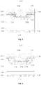
- the embodiment of the disclosure provides a cellular structure 300 of a reverse conducting IGBT that is of a plane gate structure.
- the cellular structure includes a substrate 301, a drift layer 302, a well region 303, a second conductivity type source region 304, first conductivity type source regions 305, a gate insulating layer 306, a grid 307, a conductive layer 308, an interlayer dielectric layer 309, an emitter metal layer 310, a collector region 311, a short circuit region 312 and a collector metal layer 313.
- the substrate 301 is exemplarily a first conductivity type silicon-based substrate.
- the drift layer 302 is a first conductivity type drift layer and is located on the substrate 301.
- the thickness of the drift layer 302 is selected according to a pressure-tolerant capability of a device.
- the well region 303 is a second conductivity type well region, and is located in the center of the cellular structure and arranged in a surface of the drift layer 302. A surface of the well region 303 is flush with the surface of the drift region 302.
- the second conductivity type source region 304 is a second conductivity type source region, and is arranged in the surface of the well region 303.
- the first conductivity type source regions 305 are first conductivity type source regions.
- the first conductivity type source regions 305 are arranged in the surface of the well region 303 and located at opposite sides of the second conductivity type source region 304.
- the first conductivity type source regions 305 are higher than the second conductivity type source region 304, such that parts of the bottom of the first conductivity type source regions 305 cover parts of the surfaces at the opposite sides of the second conductivity type source region 304, and the side faces of the first conductivity type source regions 305 and the surface, which is not covered with the first conductivity type source regions 305, of the second conductivity type source region 304 jointly define a main trench (not labeled in the figures).
- the above-mentioned main trench is obtained by etching a part of the second conductivity type source region 304 between two first conductivity type source regions 305 after the first conductivity type source regions 305 and the second conductivity type source region 304 are formed in the surface of the well region 303. After etching, only a part, which is located below the first conductivity type source regions 305 and below the main trench, of the second conductivity type source region 304 remains.
- the surface of second conductivity type source region 304 is more than 0.3 ⁇ m lower than the surface of first conductivity type source regions 305.
- Such structure can improve the injection level of carriers in a vertical direction.
- the gate insulating layer 306 and the grid 307 form a gate structure.
- the gate structure is a plane gate structure.
- the gate insulating layer 306 is located at opposite sides of the main trench and located on the drift layer 302.
- the gate insulating layer 306 is in contact with surfaces of the first conductivity type source regions 305, the well region 303 and the drift layer 302 at the same time, but is not in contact with the conductive layer 308.
- the gate insulating layer 306 isolates the grid 307 from the first conductivity type source regions 305, the well region 303 and the drift layer 302.
- the grid 307 is a polysilicon grid, and is arranged on the gate insulating layer 306.
- the conductive layer 308 is arranged on the bottom and a sidewall of the above-mentioned main trench, and even extends to on the first conductivity type source regions 305.
- the thickness of the conductive layer 308 is 50 nm to 200 nm, and the conductive layer 308 is a metal layer or a silicon alloy layer.
- the interlayer dielectric layer 309 is located on the grid 307, and covers parts of the conductive layer that are located on the first conductivity type source regions 305 and located on the sidewall of the main trench.
- the interlayer dielectric layer 309 isolates the grid 307, the first conductivity type source regions 305, and the parts of the conductive layer that are located on the first conductivity type source regions 305 and located on the sidewall of the main trench from the emitter metal layer 310, and also isolates the grid 307 from the first conductivity type source regions 305 and the conductive layer 308.
- the emitter metal layer 310 is located on the interlayer dielectric layer 309 and fills the above-mentioned main trench.
- the emitter metal layer 310 is in contact with a part of the conductive layer that is located on the bottom of the main trench, and is used for exporting a short circuit current of the first conductivity type source regions 305.
- the emitter metal layer 310 can be metal such as aluminum, which has low contact resistivity.
- the reverse conducting IGBT works in the FRD mode, and when the gate voltage of the reverse conducting IGBT is greater than or equal to the threshold voltage, the short circuit current of the first conductivity type source regions 305 is exported via the conductive layer 308, such that the influence of the short circuit current on the injection of the second conductivity type source region 304 is reduced, and the influence of a short circuit effect of the first conductivity type source regions 305 on FRD anode injection is reduced, thereby achieving the aim of reducing a forward turn-on voltage drop of the FRD.
- the collector region 311 is a second conductivity type collector region, and the collector region 311 is located below the substrate 301.
- the short circuit region 312 is a second conductivity type short circuit region, and the short circuit region 312 is located below the substrate 301 and adjacent to the collector region 311.
- the collector metal layer 313 is located below the collector region 311 and the short circuit region 312, and is electrically connected to the collector region 311 and the short circuit region 312.
- the cellular structure 300 can further include a storage region 314.
- the storage region 314 is a first conductivity type carrier storage region, and is arranged in the drift layer 302 and located below the well region 303.
- the doping concentration of the storage region 314 is one to two orders of magnitude higher than the doping concentration of the substrate 301.
- the storage region 314 can reduce the turn-on voltage drop of the IGBT.
- the cellular structure 300 can further include a lifetime control region 315.
- the lifetime control region 315 is arranged in the well region 303 and located below the second conductivity type source region 304.
- the lifetime control region 315 is a low lifetime control region, and the minority carrier lifetime thereof is generally three to four orders of magnitude lower than that of the other regions.
- the lifetime control region 315 is obtained by injecting other types of impurities into the well region to reduce the minority carrier lifetime, such that a switching loss of the FRD can be reduced. Through such cellular structure, both a lower forward turn-on voltage drop of the FRD and a lower switching loss of the FRD can be obtained.
- the shape of the cellular structure 300 can be honeycomb, short-strip-shaped (the cellular length ⁇ 200 ⁇ m) or long-strip-shaped.
- the first conductivity type and the second conductivity type are opposite to each other.
- the second conductivity type is the P type when the first conductivity type is the N type; and the second conductivity type is the N type when the first conductivity type is the P type.
- the disclosure provides a cellular structure of a reverse conducting IGBT that is of a plane gate structure.
- the first conductivity type source regions 305 are connected to the emitter metal layer 310 by means of the conductive layer 308, such that a coupling relationship between the first conductivity type source regions 305 and the second conductivity type source region 304 is removed; and the current of the first conductivity type source regions 305 is exported by means of the conductive layer 308, such that when the reverse conducting IGBT works in the FRD mode and the gate voltage of the reverse conducting IGBT is greater than or equal to the threshold voltage, the influence of a short circuit effect of the first conductivity type source regions on FRD anode injection is reduced, so as to reduce the influence of the gate voltage on the forward turn-on voltage drop of the FRD, and thus the FRD obtains a lower forward voltage drop.
- the embodiment of the disclosure provides a cellular structure 400 of a reverse conducting IGBT that is of a trench gate structure.
- the cellular structure includes a substrate 401, a drift layer 402, a gate insulating layer 403, a grid 404, a well region 405, a second conductivity type source region 406, first conductivity type source regions 407, a conductive layer 408, an interlayer dielectric layer 409, an emitter metal layer 410, a collector region 411, a short circuit region 412 and a collector metal layer 413.
- the substrate 401 is exemplarily a first conductivity type silicon-based substrate.
- the drift layer 402 is a first conductivity type drift layer and is located on the substrate 401.
- the thickness of the drift layer 402 is selected according to a pressure-tolerant capability of a device.
- a gate trench gate (not labeled in the figures), the insulating layer 403 and the grid 404 form a gate structure.
- the gate structure is a trench gate structure.
- the gate trench is arranged at opposite sides of the cellular structure, and located in the drift layer 402 and adjacent to the well region 405.
- the depth of the gate trench is greater than the depth of the well region 405.
- the gate insulating layer 403 is arranged on a sidewall and the bottom of the above-mentioned gate trench, and isolates the grid 404 from the first conductivity type source regions 407, the well region 405 and the drift layer 402.
- the grid 404 is a polysilicon grid, and fills the above-mentioned gate trench.
- the well region 405 is a second conductivity type well region, and is arranged in a surface of the drift layer 402 and located at the central position of the cellular structure and between two gate trenches. A surface of the well region 405 is flush with the surface of the drift layer 402. Two ends of the well region 405 are respectively in contact with the gate trenches at the opposite sides, that is, in contact with the gate insulating layers at the opposite sides.
- the second conductivity type source region 406 is a second conductivity type source region, and is arranged in the surface of the well region 405. A surface of the second conductivity type source region 406 is flush with the surface of the drift layer 402.
- the first conductivity type source regions 407 are first conductivity type source regions.
- the first conductivity type source regions 407 are arranged in the surface of the well region 405 and located at opposite sides of the second conductivity type source region 406.
- the first conductivity type source regions 407 are higher than the second conductivity type source region 406, such that parts of the bottom of the first conductivity type source regions 407 cover parts of the surfaces at the opposite sides of the second conductivity type source region 406, and the side faces of the first conductivity type source regions 407 and the surface, which is not covered with the first conductivity type source regions 407, of the second conductivity type source region 406 jointly define a main trench (not labeled in the figures).
- the above-mentioned main trench is obtained by etching a part of the second conductivity type source region 406 between two first conductivity type source regions 407 after the first conductivity type source regions 407 and the second conductivity type source region 406 are formed in the surface of the well region 405. After etching, only a part, which is located below the first conductivity type source regions 407 and below the main trench, of the second conductivity type source region 406 remains.
- the surface of second conductivity type source region 406 is more than 0.3 ⁇ m lower than the surface of first conductivity type source regions 407. Such structure can improve the injection level of carriers in a vertical direction.
- the conductive layer 408 is arranged on the bottom and a sidewall of the above-mentioned main trench, and even extends to on the first conductivity type source regions 407.
- the thickness of the conductive layer 408 is 50 nm to 200 nm, and the conductive layer 408 is a metal layer or a silicon alloy layer.
- the interlayer dielectric layer 409 is located on the grid 404, and covers both the first conductivity type source regions 407 and parts of the conductive layer that are located on the first conductivity type source regions 407 and located on the sidewall of the main trench.
- the interlayer dielectric layer 409 isolates the grid 404, the first conductivity type source regions 407, and the parts of the conductive layer that are located on the first conductivity type source regions 407 and located on the sidewall of the main trench from the emitter metal layer 410, and also isolates the grid 404 from the first conductivity type source regions 407 and the conductive layer 408.
- the emitter metal layer 410 is located on the interlayer dielectric layer 409 and fills the above-mentioned trench.
- the emitter metal layer 410 is in contact with the conductive layer that is located on the bottom of the main trench, and is used for exporting a short circuit current of the first conductivity type source regions 407.
- the emitter metal layer 410 can be metal such as aluminum, which has low contact resistivity.
- the reverse conducting IGBT works in the FRD mode, and when the gate voltage of the reverse conducting IGBT is greater than or equal to the threshold voltage, the short circuit current of the first conductivity type source regions 407 is exported via the conductive layer 408, such that the influence of the short circuit current on the injection of the second conductivity type source region 406 is reduced, and the influence of a short circuit effect of the first conductivity type source regions 407 on FRD anode injection is reduced, thereby achieving the aim of reducing a forward turn-on voltage drop of the FRD
- the collector region 411 is a second conductivity type collector region, and the collector region 411 is located below the substrate 401.
- the short circuit region 412 is a second conductivity type short circuit region, and the short circuit region 412 is located below the substrate 401 and adjacent to the collector region 411.
- the collector metal layer 413 is located below the collector region 411 and the short circuit region 412, and is electrically connected to the collector region 411 and the short circuit region 412.
- the cellular structure 400 can further include a storage region 414.
- the storage region 414 is a first conductivity type carrier storage region, and is arranged in the drift layer 402 and located below the well region 405.
- the doping concentration of the storage region 414 is one to two orders of magnitude higher than the doping concentration of the substrate 401.
- the storage region 414 can reduce the turn-on voltage drop of the IGBT.
- the cellular structure 400 can further include a lifetime control region 415.
- the lifetime control region 415 is arranged in the well region 405 and located below the second conductivity type source region 406.
- the lifetime control region 415 is a low lifetime control region, and the minority carrier lifetime thereof is generally three to four orders of magnitude lower than that of the other regions.
- the lifetime control region 415 is obtained by injecting other types of impurities into the well region to reduce the minority carrier lifetime, such that a switching loss of the FRD can be reduced. Through such cellular structure, both a lower forward turn-on voltage drop of the FRD and a lower switching loss of the FRD can be obtained.
- the shape of the cellular structure 400 can be honeycomb, short-strip-shaped (the cellular length ⁇ 200 ⁇ m) or long-strip-shaped.
- the first conductivity type and the second conductivity type are opposite to each other.
- the second conductivity type is the P type when the first conductivity type is the N type; and the second conductivity type is the N type when the first conductivity type is the P type.
- the disclosure provides a cellular structure of a reverse conducting IGBT that is of a plane gate structure.
- the first conductivity type source regions 407 are connected to the emitter metal layer 410 by means of the conductive layer 408, such that a coupling relationship between the first conductivity type source regions 407 and the second conductivity type source region 406 is removed; and the current of the first conductivity type source regions 407 is exported by means of the conductive layer 408, such that when the reverse conducting IGBT works in the FRD mode and the gate voltage of the reverse conducting IGBT is greater than or equal to the threshold voltage, the influence of a short circuit effect of the first conductivity type source regions 407 on FRD anode injection is reduced, so as to reduce the influence of the gate voltage on the forward turn-on voltage drop of the FRD, and thus the FRD obtains a lower forward voltage drop.
Landscapes
- Metal-Oxide And Bipolar Metal-Oxide Semiconductor Integrated Circuits (AREA)
- Electrodes Of Semiconductors (AREA)
Applications Claiming Priority (2)
| Application Number | Priority Date | Filing Date | Title |
|---|---|---|---|
| CN201911366131.0A CN113053991A (zh) | 2019-12-26 | 2019-12-26 | 逆导型igbt的元胞结构及逆导型igbt |
| PCT/CN2020/084136 WO2021128653A1 (zh) | 2019-12-26 | 2020-04-10 | 逆导型igbt的元胞结构及逆导型igbt |
Publications (2)
| Publication Number | Publication Date |
|---|---|
| EP4084084A1 true EP4084084A1 (de) | 2022-11-02 |
| EP4084084A4 EP4084084A4 (de) | 2024-01-24 |
Family
ID=76505377
Family Applications (1)
| Application Number | Title | Priority Date | Filing Date |
|---|---|---|---|
| EP20907435.0A Pending EP4084084A4 (de) | 2019-12-26 | 2020-04-10 | Zelluläre struktur von igbt mit umgekehrter leitung und igbt mit umgekehrter leitung |
Country Status (3)
| Country | Link |
|---|---|
| EP (1) | EP4084084A4 (de) |
| CN (1) | CN113053991A (de) |
| WO (1) | WO2021128653A1 (de) |
Families Citing this family (1)
| Publication number | Priority date | Publication date | Assignee | Title |
|---|---|---|---|---|
| CN117650161B (zh) * | 2023-10-31 | 2024-08-16 | 海信家电集团股份有限公司 | 半导体装置和半导体装置的制造方法 |
Family Cites Families (12)
| Publication number | Priority date | Publication date | Assignee | Title |
|---|---|---|---|---|
| DE10261424B3 (de) * | 2002-12-30 | 2004-07-01 | Infineon Technologies Ag | Verfahren zum Herstellen eines Emitters mit niedrigem Emitterwirkungsgrad |
| JP4952638B2 (ja) * | 2008-04-07 | 2012-06-13 | トヨタ自動車株式会社 | 半導体素子と半導体装置とその駆動方法 |
| US20100117117A1 (en) * | 2008-11-10 | 2010-05-13 | Infineon Technologies Ag | Vertical IGBT Device |
| JP2010238738A (ja) * | 2009-03-30 | 2010-10-21 | Toshiba Corp | 半導体装置および半導体装置の製造方法 |
| US20110062489A1 (en) * | 2009-09-11 | 2011-03-17 | Disney Donald R | Power device with self-aligned silicide contact |
| US9209109B2 (en) * | 2013-07-15 | 2015-12-08 | Infineon Technologies Ag | IGBT with emitter electrode electrically connected with an impurity zone |
| US9240450B2 (en) * | 2014-02-12 | 2016-01-19 | Infineon Technologies Ag | IGBT with emitter electrode electrically connected with impurity zone |
| WO2016010097A1 (ja) * | 2014-07-17 | 2016-01-21 | 富士電機株式会社 | 半導体装置および半導体装置の製造方法 |
| EP3154091A1 (de) * | 2015-10-07 | 2017-04-12 | ABB Technology AG | Rückwärtsleitendes halbleiterbauelement |
| DE112017000727T5 (de) * | 2016-09-14 | 2018-10-31 | Fuji Electric Co., Ltd. | RC-IGBT und Herstellungsverfahren dafür |
| JP6988175B2 (ja) * | 2017-06-09 | 2022-01-05 | 富士電機株式会社 | 炭化珪素半導体装置および炭化珪素半導体装置の製造方法 |
| JP2019091796A (ja) * | 2017-11-14 | 2019-06-13 | トヨタ自動車株式会社 | スイッチング素子とその製造方法 |
-
2019
- 2019-12-26 CN CN201911366131.0A patent/CN113053991A/zh active Pending
-
2020
- 2020-04-10 EP EP20907435.0A patent/EP4084084A4/de active Pending
- 2020-04-10 WO PCT/CN2020/084136 patent/WO2021128653A1/zh not_active Ceased
Also Published As
| Publication number | Publication date |
|---|---|
| EP4084084A4 (de) | 2024-01-24 |
| CN113053991A (zh) | 2021-06-29 |
| WO2021128653A1 (zh) | 2021-07-01 |
Similar Documents
| Publication | Publication Date | Title |
|---|---|---|
| US12543359B2 (en) | Cellular structure of silicon carbide MOSFET device, and silicon carbide MOSFET device | |
| US10692861B2 (en) | Method of manufacturing a semiconductor device | |
| JP5392959B2 (ja) | 半導体デバイスおよび半導体デバイスを形成する方法 | |
| US10134888B2 (en) | Semiconductor device and method of manufacturing the same | |
| JP4696337B2 (ja) | 半導体装置 | |
| CN116722038A (zh) | 半导体装置 | |
| US11398472B2 (en) | RC IGBT with an IGBT section and a diode section | |
| US11469317B2 (en) | Rc igbt | |
| CN115483281B (zh) | 逆导型横向绝缘栅双极型晶体管 | |
| CN106997899A (zh) | 一种igbt器件及其制备方法 | |
| US11264475B2 (en) | Semiconductor device having a gate electrode formed in a trench structure | |
| US11538906B2 (en) | Diode with structured barrier region | |
| WO2016101134A1 (zh) | 一种双向mos型器件及其制造方法 | |
| CN114823886B (zh) | 提升转换效率的沟槽型rc-igbt器件及制备方法 | |
| KR20190113644A (ko) | 니들 셀 트렌치 mosfet | |
| US11949006B2 (en) | Power semiconductor device with p-contact and doped insulation blocks defining contact holes | |
| EP4084084A1 (de) | Zelluläre struktur von igbt mit umgekehrter leitung und igbt mit umgekehrter leitung | |
| US12211903B2 (en) | Semiconductor device and method for designing thereof | |
| CN120224711B (zh) | 半导体器件及其制备方法 | |
| CN224139373U (zh) | 一种非对称高可靠沟槽栅碳化硅vdmos | |
| US20260096166A1 (en) | Power semiconductor device and method of producing a power semiconductor device | |
| KR20250146535A (ko) | 전력 반도체 소자 및 전력 반도체 칩 | |
| CN119451210A (zh) | 功率器件及其制造方法 | |
| CN111180511A (zh) | 一种绝缘闸双极晶体管与整流器之整合结构的制造方法 |
Legal Events
| Date | Code | Title | Description |
|---|---|---|---|
| STAA | Information on the status of an ep patent application or granted ep patent |
Free format text: STATUS: THE INTERNATIONAL PUBLICATION HAS BEEN MADE |
|
| PUAI | Public reference made under article 153(3) epc to a published international application that has entered the european phase |
Free format text: ORIGINAL CODE: 0009012 |
|
| STAA | Information on the status of an ep patent application or granted ep patent |
Free format text: STATUS: REQUEST FOR EXAMINATION WAS MADE |
|
| 17P | Request for examination filed |
Effective date: 20220701 |
|
| AK | Designated contracting states |
Kind code of ref document: A1 Designated state(s): AL AT BE BG CH CY CZ DE DK EE ES FI FR GB GR HR HU IE IS IT LI LT LU LV MC MK MT NL NO PL PT RO RS SE SI SK SM TR |
|
| DAV | Request for validation of the european patent (deleted) | ||
| DAX | Request for extension of the european patent (deleted) | ||
| P01 | Opt-out of the competence of the unified patent court (upc) registered |
Effective date: 20230601 |
|
| A4 | Supplementary search report drawn up and despatched |
Effective date: 20240104 |
|
| RIC1 | Information provided on ipc code assigned before grant |
Ipc: H01L 29/36 20060101ALN20231221BHEP Ipc: H01L 29/08 20060101ALI20231221BHEP Ipc: H01L 29/10 20060101ALI20231221BHEP Ipc: H01L 29/417 20060101ALI20231221BHEP Ipc: H01L 29/40 20060101ALI20231221BHEP Ipc: H01L 29/739 20060101AFI20231221BHEP |