EP4084005A1 - Verfahren und system zur reparatur einer speichervorrichtung - Google Patents
Verfahren und system zur reparatur einer speichervorrichtung Download PDFInfo
- Publication number
- EP4084005A1 EP4084005A1 EP21772941.7A EP21772941A EP4084005A1 EP 4084005 A1 EP4084005 A1 EP 4084005A1 EP 21772941 A EP21772941 A EP 21772941A EP 4084005 A1 EP4084005 A1 EP 4084005A1
- Authority
- EP
- European Patent Office
- Prior art keywords
- repairing
- row address
- unit
- row
- memory device
- Prior art date
- Legal status (The legal status is an assumption and is not a legal conclusion. Google has not performed a legal analysis and makes no representation as to the accuracy of the status listed.)
- Granted
Links
Images
Classifications
-
- G—PHYSICS
- G11—INFORMATION STORAGE
- G11C—STATIC STORES
- G11C29/00—Checking stores for correct operation ; Subsequent repair; Testing stores during standby or offline operation
- G11C29/04—Detection or location of defective memory elements, e.g. cell constructio details, timing of test signals
- G11C29/08—Functional testing, e.g. testing during refresh, power-on self testing [POST] or distributed testing
- G11C29/12—Built-in arrangements for testing, e.g. built-in self testing [BIST] or interconnection details
- G11C29/44—Indication or identification of errors, e.g. for repair
- G11C29/4401—Indication or identification of errors, e.g. for repair for self repair
-
- G—PHYSICS
- G06—COMPUTING OR CALCULATING; COUNTING
- G06F—ELECTRIC DIGITAL DATA PROCESSING
- G06F11/00—Error detection; Error correction; Monitoring
- G06F11/07—Responding to the occurrence of a fault, e.g. fault tolerance
- G06F11/16—Error detection or correction of the data by redundancy in hardware
- G06F11/20—Error detection or correction of the data by redundancy in hardware using active fault-masking, e.g. by switching out faulty elements or by switching in spare elements
- G06F11/2053—Error detection or correction of the data by redundancy in hardware using active fault-masking, e.g. by switching out faulty elements or by switching in spare elements where persistent mass storage functionality or persistent mass storage control functionality is redundant
- G06F11/2094—Redundant storage or storage space
-
- G—PHYSICS
- G06—COMPUTING OR CALCULATING; COUNTING
- G06F—ELECTRIC DIGITAL DATA PROCESSING
- G06F3/00—Input arrangements for transferring data to be processed into a form capable of being handled by the computer; Output arrangements for transferring data from processing unit to output unit, e.g. interface arrangements
- G06F3/06—Digital input from, or digital output to, record carriers, e.g. RAID, emulated record carriers or networked record carriers
- G06F3/0601—Interfaces specially adapted for storage systems
- G06F3/0602—Interfaces specially adapted for storage systems specifically adapted to achieve a particular effect
- G06F3/0614—Improving the reliability of storage systems
- G06F3/0619—Improving the reliability of storage systems in relation to data integrity, e.g. data losses, bit errors
-
- G—PHYSICS
- G06—COMPUTING OR CALCULATING; COUNTING
- G06F—ELECTRIC DIGITAL DATA PROCESSING
- G06F3/00—Input arrangements for transferring data to be processed into a form capable of being handled by the computer; Output arrangements for transferring data from processing unit to output unit, e.g. interface arrangements
- G06F3/06—Digital input from, or digital output to, record carriers, e.g. RAID, emulated record carriers or networked record carriers
- G06F3/0601—Interfaces specially adapted for storage systems
- G06F3/0628—Interfaces specially adapted for storage systems making use of a particular technique
- G06F3/0653—Monitoring storage devices or systems
-
- G—PHYSICS
- G06—COMPUTING OR CALCULATING; COUNTING
- G06F—ELECTRIC DIGITAL DATA PROCESSING
- G06F3/00—Input arrangements for transferring data to be processed into a form capable of being handled by the computer; Output arrangements for transferring data from processing unit to output unit, e.g. interface arrangements
- G06F3/06—Digital input from, or digital output to, record carriers, e.g. RAID, emulated record carriers or networked record carriers
- G06F3/0601—Interfaces specially adapted for storage systems
- G06F3/0668—Interfaces specially adapted for storage systems adopting a particular infrastructure
- G06F3/0671—In-line storage system
- G06F3/0673—Single storage device
-
- G—PHYSICS
- G11—INFORMATION STORAGE
- G11C—STATIC STORES
- G11C29/00—Checking stores for correct operation ; Subsequent repair; Testing stores during standby or offline operation
- G11C29/70—Masking faults in memories by using spares or by reconfiguring
- G11C29/72—Masking faults in memories by using spares or by reconfiguring with optimized replacement algorithms
-
- G—PHYSICS
- G11—INFORMATION STORAGE
- G11C—STATIC STORES
- G11C29/00—Checking stores for correct operation ; Subsequent repair; Testing stores during standby or offline operation
- G11C29/70—Masking faults in memories by using spares or by reconfiguring
- G11C29/78—Masking faults in memories by using spares or by reconfiguring using programmable devices
- G11C29/785—Masking faults in memories by using spares or by reconfiguring using programmable devices with redundancy programming schemes
- G11C29/789—Masking faults in memories by using spares or by reconfiguring using programmable devices with redundancy programming schemes using non-volatile cells or latches
-
- G—PHYSICS
- G11—INFORMATION STORAGE
- G11C—STATIC STORES
- G11C29/00—Checking stores for correct operation ; Subsequent repair; Testing stores during standby or offline operation
- G11C29/70—Masking faults in memories by using spares or by reconfiguring
- G11C29/78—Masking faults in memories by using spares or by reconfiguring using programmable devices
- G11C29/835—Masking faults in memories by using spares or by reconfiguring using programmable devices with roll call arrangements for redundant substitutions
-
- G—PHYSICS
- G11—INFORMATION STORAGE
- G11C—STATIC STORES
- G11C29/00—Checking stores for correct operation ; Subsequent repair; Testing stores during standby or offline operation
- G11C29/04—Detection or location of defective memory elements, e.g. cell constructio details, timing of test signals
- G11C29/08—Functional testing, e.g. testing during refresh, power-on self testing [POST] or distributed testing
- G11C29/12—Built-in arrangements for testing, e.g. built-in self testing [BIST] or interconnection details
- G11C2029/1202—Word line control
-
- G—PHYSICS
- G11—INFORMATION STORAGE
- G11C—STATIC STORES
- G11C29/00—Checking stores for correct operation ; Subsequent repair; Testing stores during standby or offline operation
- G11C29/04—Detection or location of defective memory elements, e.g. cell constructio details, timing of test signals
- G11C29/08—Functional testing, e.g. testing during refresh, power-on self testing [POST] or distributed testing
- G11C29/12—Built-in arrangements for testing, e.g. built-in self testing [BIST] or interconnection details
- G11C2029/1208—Error catch memory
-
- G—PHYSICS
- G11—INFORMATION STORAGE
- G11C—STATIC STORES
- G11C29/00—Checking stores for correct operation ; Subsequent repair; Testing stores during standby or offline operation
- G11C29/04—Detection or location of defective memory elements, e.g. cell constructio details, timing of test signals
- G11C29/08—Functional testing, e.g. testing during refresh, power-on self testing [POST] or distributed testing
- G11C29/12—Built-in arrangements for testing, e.g. built-in self testing [BIST] or interconnection details
- G11C2029/4402—Internal storage of test result, quality data, chip identification, repair information
-
- G—PHYSICS
- G11—INFORMATION STORAGE
- G11C—STATIC STORES
- G11C29/00—Checking stores for correct operation ; Subsequent repair; Testing stores during standby or offline operation
- G11C29/04—Detection or location of defective memory elements, e.g. cell constructio details, timing of test signals
- G11C29/08—Functional testing, e.g. testing during refresh, power-on self testing [POST] or distributed testing
- G11C29/12—Built-in arrangements for testing, e.g. built-in self testing [BIST] or interconnection details
- G11C29/38—Response verification devices
- G11C29/42—Response verification devices using error correcting codes [ECC] or parity check
-
- G—PHYSICS
- G11—INFORMATION STORAGE
- G11C—STATIC STORES
- G11C29/00—Checking stores for correct operation ; Subsequent repair; Testing stores during standby or offline operation
- G11C29/52—Protection of memory contents; Detection of errors in memory contents
-
- G—PHYSICS
- G11—INFORMATION STORAGE
- G11C—STATIC STORES
- G11C29/00—Checking stores for correct operation ; Subsequent repair; Testing stores during standby or offline operation
- G11C29/70—Masking faults in memories by using spares or by reconfiguring
- G11C29/78—Masking faults in memories by using spares or by reconfiguring using programmable devices
- G11C29/80—Masking faults in memories by using spares or by reconfiguring using programmable devices with improved layout
- G11C29/804—Masking faults in memories by using spares or by reconfiguring using programmable devices with improved layout to prevent clustered faults
-
- G—PHYSICS
- G11—INFORMATION STORAGE
- G11C—STATIC STORES
- G11C29/00—Checking stores for correct operation ; Subsequent repair; Testing stores during standby or offline operation
- G11C29/70—Masking faults in memories by using spares or by reconfiguring
- G11C29/78—Masking faults in memories by using spares or by reconfiguring using programmable devices
- G11C29/80—Masking faults in memories by using spares or by reconfiguring using programmable devices with improved layout
- G11C29/81—Masking faults in memories by using spares or by reconfiguring using programmable devices with improved layout using a hierarchical redundancy scheme
Definitions
- the reference storage module may store the repaired row address. At this time, before repairing, storage may not be performed in the reference storage module. During the repairing process, the row address stored in the reference storage module may be gradually increased, thereby effectively reducing system memory and improving a repairing efficiency.
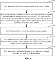
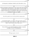
- the method may further include the following step of S600.
- steps in the flow chart of FIG. 1 are successively displayed according to the indication of an arrow, these steps are not certainly performed according to the order indicated by the arrow. Unless otherwise stated herein, the implementation of these steps has no strict order limitation, and these steps may be performed according to another order. Moreover, at least part of the steps in FIG. 1 may include a plurality of steps or a plurality of stages. These steps or stages are not certainly competed at the same time, and performed at different times. The implementation order of these steps or stages is not certainly carried in turn, and in turn or alternatively performed together with at least part of the steps or stages in other steps or stages.
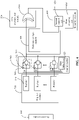
- a respective one of the registers 210 is configured to receive and temporarily store a unit address of each of the error units and output a row address in the unit address of each of the error units, each of the error units occupies a respective one of the registers, and each of the unit addresses includes a row address.
- the control module 300 is electrically connected with the registers 210 and configured to successively select one of the registers, as a target register, in response to that the number of the error units detected by the detection module 100 reaches the first preset number.
- the reference storage module 400 is configured to store and output a repaired row addresses or an unrepaired row address.
- the first determination module 500 is electrically connected with the reference storage module 400 and the register module 200, configured to receive a row address output by the target register 210 and a row address output by the reference storage module 400, to determine whether the row address in the target register exists in the reference storage module. And the first determination module 500 is further configured to output a result of the determination.
- the control module 300 may include a first control unit 320 and n switch units 310, each of the switch units 310 may correspond to a respective one of the registers 210, and n is a positive integer greater than 1.
- the manner in which the first control unit 320 controls the opening of the kth switch unit may be as the following.
- the control signal Sk input by the first control unit 320 to the kth switch unit 310 may be a high-level signal, and the NMOS tube may receive the high-level signal.
- the inverter 312 may receive the high-level signal, and the high-level signal may be converted into a low-level signal and output to the PMOS tube. Therefore, at least one of the NMOS tube or the PMOS tube can be conducted at this time, thereby opening the switch unit 310.
- the NMOS tube may receive the low-level signal.
- the inverter 312 may receive the low-level signal, and the low-level signal may be converted into a high-level signal and output to the PMOS tube. Therefore, at least one of the NMOS tube or the PMOS tube can be conducted at this time, thereby disconnecting the switch unit 310.
- the repairing module 600 is electrically connected with the first determination module 500 and configured to repair error units that are not repaired through the row address according to the result of the determination.
- the comparator 510 may output a high-level signal to open the repairing module 600, and the error unit corresponding to the target register 210 may be repaired.
- the comparator 510 may output a low-level signal, and then the repairing module 600 may not be opened.
- the comparator 510 may successively compare whether the row address output by the target register 210 is consistent with each of the row addresses stored in the reference storage module 400.
- the repairing module 600 may include a row repairing unit 610 and a second control unit 620.
- the row repairing unit 610 may be electrically connected with the respective one of the registers 210 and configured to perform a row address repairing on the error unit corresponding to the target register.
- the second control unit 620 may be electrically connected with the comparator 510 and the row repairing unit 610, and configured to open/close the row repairing unit according to a high-level signal or a low-level signal output by the comparator 510.
- the second control unit 620 may further include a switch transistor and other switch devices.
- the switch transistor and other switch devices When the high-level signal output by the comparator 510 is received, the switch transistor and other switch devices may be opened to open the row repairing unit 610, so as to perform the row address repairing on the error unit corresponding to the target register.
- the switch transistor and other switch devices When the low-level signal output by the comparator 510 is received, the switch transistor and other switch devices may be disconnected to close the row repairing unit 610, so as to skip the repairing on the error unit corresponding to the target register, or terminate this repairing process.
- control module 300 may include a first control unit 320 and n switch units 310, each of the switch units 310 may correspond to a respective one of the registers 210, and n is a positive integer greater than 1.
- the first control unit 320 may respectively input control signals S1-Sn to the n switch units 310.
- a control signal input by the first control unit 320 to a kth switch unit 310 may be Sk, and k is greater than or equal to 1, or less than or equal to n.
- remaining control signals may be low-level signals.
- the corresponding switch unit 310 may be opened. Therefore, the row address in the target register may be transmitted to the first determination module 500 and the repairing module 600.
- the comparator 510 of the first determination module 500 may directly obtain the row address in the target register, and compare the row address in the target register with the row address output by the reference storage module 400. And then, the level signal may be output according to a comparison result.
- the row repairing unit 610 may receive and store the row address in the target register. And then, the row address in the target register may be stored in the row repairing unit 610 to be repaired.
- the row repairing unit 610 may include a second preset number of row repairing fuses.
- One row repairing fuse may correspond to one redundant row address.
- the row repairing unit 610 may be configured to store the row address in the target register to one blank row repairing fuse of the row repairing unit 610.
- the reference storage module 400 may include the row repairing unit 610.
- system for repairing the memory device may further include a second determination module (not shown in the figure), and the second determination module may be configured to determine whether there is a blank row repairing fuse in the row repairing unit 610.
- the second control unit 620 may open the row repairing unit 600, in response to that the row address of the target register does not exist in the reference storage module 400 and the row repairing unit 610 has a blank row repairing fuse.
- the unit address may further include a column address.
- the repairing module 600 may further include a column repairing unit (not shown in the figure), and the column repairing unit may be configured to repair a column address of the error unit corresponding to the target register.
- the second control unit may open the column repairing unit in response to that the row address of the target register does not exist in the reference storage module and the row repairing unit has a blank row repairing fuse.
- Each module in the foregoing system for repairing the memory device may be implemented in whole or in part by software, hardware or a combination thereof.
- Each of the foregoing modules may be embedded in the form of hardware or independent of a processor in a computer device, or be stored in memory of the computer device in the form of software, so that the processor may call and execute operations corresponding to the foregoing modules.
- the division of the module is schematic, and is only a logic function division, and there may be other division forms in actual implementations.
Landscapes
- Engineering & Computer Science (AREA)
- Theoretical Computer Science (AREA)
- Physics & Mathematics (AREA)
- General Engineering & Computer Science (AREA)
- General Physics & Mathematics (AREA)
- Human Computer Interaction (AREA)
- Computer Security & Cryptography (AREA)
- Quality & Reliability (AREA)
- Techniques For Improving Reliability Of Storages (AREA)
- For Increasing The Reliability Of Semiconductor Memories (AREA)
Applications Claiming Priority (2)
| Application Number | Priority Date | Filing Date | Title |
|---|---|---|---|
| CN202110295405.2A CN115116531B (zh) | 2021-03-19 | 2021-03-19 | 存储器件修复方法及系统 |
| PCT/CN2021/103481 WO2022193471A1 (zh) | 2021-03-19 | 2021-06-30 | 存储器件修复方法及系统 |
Publications (3)
| Publication Number | Publication Date |
|---|---|
| EP4084005A1 true EP4084005A1 (de) | 2022-11-02 |
| EP4084005A4 EP4084005A4 (de) | 2022-11-02 |
| EP4084005B1 EP4084005B1 (de) | 2023-06-07 |
Family
ID=83284812
Family Applications (1)
| Application Number | Title | Priority Date | Filing Date |
|---|---|---|---|
| EP21772941.7A Active EP4084005B1 (de) | 2021-03-19 | 2021-06-30 | Verfahren und system zur reparatur einer speichervorrichtung |
Country Status (2)
| Country | Link |
|---|---|
| US (1) | US12026073B2 (de) |
| EP (1) | EP4084005B1 (de) |
Families Citing this family (1)
| Publication number | Priority date | Publication date | Assignee | Title |
|---|---|---|---|---|
| CN119007786B (zh) * | 2023-05-19 | 2025-10-03 | 兆易创新科技集团股份有限公司 | 存储装置的修复方法及存储装置的修复系统 |
Family Cites Families (14)
| Publication number | Priority date | Publication date | Assignee | Title |
|---|---|---|---|---|
| US20020196687A1 (en) * | 2001-06-08 | 2002-12-26 | Sauvageau Anthony J. | Methods and apparatus for analyzing and repairing memory |
| US7565585B2 (en) * | 2004-01-13 | 2009-07-21 | International Business Machines Corporation | Integrated redundancy architecture and method for providing redundancy allocation to an embedded memory system |
| CN101329918A (zh) | 2008-07-30 | 2008-12-24 | 中国科学院计算技术研究所 | 存储器内建自修复系统及自修复方法 |
| CN102237132B (zh) | 2010-05-06 | 2014-01-22 | 复旦大学 | 一种存储器 |
| CN102592680B (zh) | 2011-01-12 | 2015-04-08 | 北京兆易创新科技股份有限公司 | 一种存储芯片的修复装置和方法 |
| CN102420016A (zh) | 2011-11-03 | 2012-04-18 | 西安交通大学 | 一种应用于集成错误校验码的嵌入式存储器的内建修复分析方法 |
| US9953725B2 (en) * | 2012-02-29 | 2018-04-24 | Samsung Electronics Co., Ltd. | Semiconductor memory devices and methods of operating the same |
| US8942051B2 (en) | 2012-07-27 | 2015-01-27 | Taiwan Semiconductor Manufacturing Company, Ltd. | Mechanisms for built-in self test and repair for memory devices |
| US9165679B2 (en) * | 2012-09-18 | 2015-10-20 | Samsung Electronics Co., Ltd. | Post package repairing method, method of preventing multiple activation of spare word lines, and semiconductor memory device including fuse programming circuit |
| US10443531B2 (en) * | 2017-08-18 | 2019-10-15 | Micron Technology, Inc. | Apparatuses and methods for storing redundancy repair information for memories |
| KR102384733B1 (ko) | 2017-09-26 | 2022-04-08 | 삼성전자주식회사 | 반도체 메모리 장치, 반도체 메모리 장치의 동작 방법 및 메모리 시스템 |
| KR20190048132A (ko) | 2017-10-30 | 2019-05-09 | 삼성전자주식회사 | 페일 어드레스의 중복 프로그램을 방지하기 위한 메모리 장치 및 그것의 동작 방법 |
| KR102573833B1 (ko) * | 2018-04-18 | 2023-09-04 | 에스케이하이닉스 주식회사 | 메모리에 대한 테스트 회로 및 이를 포함하는 메모리 모듈 |
| KR102556939B1 (ko) * | 2019-04-15 | 2023-07-20 | 에스케이하이닉스 주식회사 | 오티피 메모리 회로 및 이를 포함하는 반도체 장치 |
-
2021
- 2021-06-30 EP EP21772941.7A patent/EP4084005B1/de active Active
- 2021-08-17 US US17/404,119 patent/US12026073B2/en active Active
Also Published As
| Publication number | Publication date |
|---|---|
| EP4084005B1 (de) | 2023-06-07 |
| EP4084005A4 (de) | 2022-11-02 |
| US20220300388A1 (en) | 2022-09-22 |
| US12026073B2 (en) | 2024-07-02 |
Similar Documents
| Publication | Publication Date | Title |
|---|---|---|
| US7848899B2 (en) | Systems and methods for testing integrated circuit devices | |
| US10699796B2 (en) | Validation of a repair to a selected row of data | |
| EP3407355A1 (de) | Speichersystem mit niedriger leseleistung | |
| US7808825B2 (en) | Non-volatile memory device and method of programming the same | |
| US20050138513A1 (en) | Multiple on-chip test runs and repairs for memories | |
| US8477547B2 (en) | Semiconductor memory device and method of operating the same | |
| EP0096782A2 (de) | On-Line Neuausrichtung von Speicherfehlern | |
| US10714201B2 (en) | Memory system capable of pre-screening internal transistors | |
| US20170024273A1 (en) | Repair information providing device in an integrated circuit | |
| KR100265764B1 (ko) | 다수군의 데이터 입출력 채널들 중 어느 일군이 선택되어 테스트되는 반도체 메모리장치 | |
| EP4084005A1 (de) | Verfahren und system zur reparatur einer speichervorrichtung | |
| CN112634960B (zh) | 存储器及其寻址方法 | |
| US7729169B2 (en) | Multiple programming of spare memory region for nonvolatile memory | |
| CN216485391U (zh) | 支持乱序成品测试的芯片 | |
| CN115116531B (zh) | 存储器件修复方法及系统 | |
| US6910161B2 (en) | Device and method for reducing the number of addresses of faulty memory cells | |
| JPH076597A (ja) | メモリ内の欠陥素子の処理方法 | |
| US6654301B2 (en) | Multiple discharge capable bit line | |
| US5828673A (en) | Logical check apparatus and method for semiconductor circuits and storage medium storing logical check program for semiconductor circuits | |
| CN101083142A (zh) | 半导体器件 | |
| US20040153904A1 (en) | [memory architecture and method for repairing a serial access memory] | |
| EP0618587A1 (de) | Halbleiterspeicher mit Speichermatrix, der mit einem einzigen Sektor assoziierte Redundantezellenspalte enthält | |
| US7512022B2 (en) | Non-volatile memory structure | |
| US20080144379A1 (en) | Implementation of column redundancy for a flash memory with a high write parallelism | |
| CN112309468B (zh) | 用于快速读取的存储器装置及其控制方法 |
Legal Events
| Date | Code | Title | Description |
|---|---|---|---|
| STAA | Information on the status of an ep patent application or granted ep patent |
Free format text: STATUS: UNKNOWN |
|
| STAA | Information on the status of an ep patent application or granted ep patent |
Free format text: STATUS: THE INTERNATIONAL PUBLICATION HAS BEEN MADE |
|
| PUAI | Public reference made under article 153(3) epc to a published international application that has entered the european phase |
Free format text: ORIGINAL CODE: 0009012 |
|
| STAA | Information on the status of an ep patent application or granted ep patent |
Free format text: STATUS: REQUEST FOR EXAMINATION WAS MADE |
|
| 17P | Request for examination filed |
Effective date: 20210928 |
|
| A4 | Supplementary search report drawn up and despatched |
Effective date: 20220909 |
|
| AK | Designated contracting states |
Kind code of ref document: A1 Designated state(s): AL AT BE BG CH CY CZ DE DK EE ES FI FR GB GR HR HU IE IS IT LI LT LU LV MC MK MT NL NO PL PT RO RS SE SI SK SM TR |
|
| RIC1 | Information provided on ipc code assigned before grant |
Ipc: G11C 29/52 20060101ALN20230216BHEP Ipc: G11C 29/42 20060101ALN20230216BHEP Ipc: G11C 29/12 20060101ALN20230216BHEP Ipc: G11C 29/44 20060101ALI20230216BHEP Ipc: G11C 29/00 20060101AFI20230216BHEP |
|
| GRAP | Despatch of communication of intention to grant a patent |
Free format text: ORIGINAL CODE: EPIDOSNIGR1 |
|
| STAA | Information on the status of an ep patent application or granted ep patent |
Free format text: STATUS: GRANT OF PATENT IS INTENDED |
|
| RIC1 | Information provided on ipc code assigned before grant |
Ipc: G11C 29/52 20060101ALN20230302BHEP Ipc: G11C 29/42 20060101ALN20230302BHEP Ipc: G11C 29/12 20060101ALN20230302BHEP Ipc: G11C 29/44 20060101ALI20230302BHEP Ipc: G11C 29/00 20060101AFI20230302BHEP |
|
| DAV | Request for validation of the european patent (deleted) | ||
| DAX | Request for extension of the european patent (deleted) | ||
| INTG | Intention to grant announced |
Effective date: 20230328 |
|
| GRAS | Grant fee paid |
Free format text: ORIGINAL CODE: EPIDOSNIGR3 |
|
| GRAA | (expected) grant |
Free format text: ORIGINAL CODE: 0009210 |
|
| STAA | Information on the status of an ep patent application or granted ep patent |
Free format text: STATUS: THE PATENT HAS BEEN GRANTED |
|
| AK | Designated contracting states |
Kind code of ref document: B1 Designated state(s): AL AT BE BG CH CY CZ DE DK EE ES FI FR GB GR HR HU IE IS IT LI LT LU LV MC MK MT NL NO PL PT RO RS SE SI SK SM TR |
|
| REG | Reference to a national code |
Ref country code: GB Ref legal event code: FG4D |
|
| REG | Reference to a national code |
Ref country code: CH Ref legal event code: EP Ref country code: AT Ref legal event code: REF Ref document number: 1577412 Country of ref document: AT Kind code of ref document: T Effective date: 20230615 |
|
| REG | Reference to a national code |
Ref country code: DE Ref legal event code: R096 Ref document number: 602021002852 Country of ref document: DE |
|
| P01 | Opt-out of the competence of the unified patent court (upc) registered |
Effective date: 20230531 |
|
| REG | Reference to a national code |
Ref country code: LT Ref legal event code: MG9D |
|
| REG | Reference to a national code |
Ref country code: NL Ref legal event code: MP Effective date: 20230607 |
|
| PG25 | Lapsed in a contracting state [announced via postgrant information from national office to epo] |
Ref country code: SE Free format text: LAPSE BECAUSE OF FAILURE TO SUBMIT A TRANSLATION OF THE DESCRIPTION OR TO PAY THE FEE WITHIN THE PRESCRIBED TIME-LIMIT Effective date: 20230607 Ref country code: NO Free format text: LAPSE BECAUSE OF FAILURE TO SUBMIT A TRANSLATION OF THE DESCRIPTION OR TO PAY THE FEE WITHIN THE PRESCRIBED TIME-LIMIT Effective date: 20230907 Ref country code: ES Free format text: LAPSE BECAUSE OF FAILURE TO SUBMIT A TRANSLATION OF THE DESCRIPTION OR TO PAY THE FEE WITHIN THE PRESCRIBED TIME-LIMIT Effective date: 20230607 |
|
| REG | Reference to a national code |
Ref country code: AT Ref legal event code: MK05 Ref document number: 1577412 Country of ref document: AT Kind code of ref document: T Effective date: 20230607 |
|
| PG25 | Lapsed in a contracting state [announced via postgrant information from national office to epo] |
Ref country code: RS Free format text: LAPSE BECAUSE OF FAILURE TO SUBMIT A TRANSLATION OF THE DESCRIPTION OR TO PAY THE FEE WITHIN THE PRESCRIBED TIME-LIMIT Effective date: 20230607 Ref country code: NL Free format text: LAPSE BECAUSE OF FAILURE TO SUBMIT A TRANSLATION OF THE DESCRIPTION OR TO PAY THE FEE WITHIN THE PRESCRIBED TIME-LIMIT Effective date: 20230607 Ref country code: LV Free format text: LAPSE BECAUSE OF FAILURE TO SUBMIT A TRANSLATION OF THE DESCRIPTION OR TO PAY THE FEE WITHIN THE PRESCRIBED TIME-LIMIT Effective date: 20230607 Ref country code: LT Free format text: LAPSE BECAUSE OF FAILURE TO SUBMIT A TRANSLATION OF THE DESCRIPTION OR TO PAY THE FEE WITHIN THE PRESCRIBED TIME-LIMIT Effective date: 20230607 Ref country code: HR Free format text: LAPSE BECAUSE OF FAILURE TO SUBMIT A TRANSLATION OF THE DESCRIPTION OR TO PAY THE FEE WITHIN THE PRESCRIBED TIME-LIMIT Effective date: 20230607 Ref country code: GR Free format text: LAPSE BECAUSE OF FAILURE TO SUBMIT A TRANSLATION OF THE DESCRIPTION OR TO PAY THE FEE WITHIN THE PRESCRIBED TIME-LIMIT Effective date: 20230908 |
|
| PG25 | Lapsed in a contracting state [announced via postgrant information from national office to epo] |
Ref country code: FI Free format text: LAPSE BECAUSE OF FAILURE TO SUBMIT A TRANSLATION OF THE DESCRIPTION OR TO PAY THE FEE WITHIN THE PRESCRIBED TIME-LIMIT Effective date: 20230607 |
|
| PG25 | Lapsed in a contracting state [announced via postgrant information from national office to epo] |
Ref country code: SK Free format text: LAPSE BECAUSE OF FAILURE TO SUBMIT A TRANSLATION OF THE DESCRIPTION OR TO PAY THE FEE WITHIN THE PRESCRIBED TIME-LIMIT Effective date: 20230607 |
|
| PG25 | Lapsed in a contracting state [announced via postgrant information from national office to epo] |
Ref country code: IS Free format text: LAPSE BECAUSE OF FAILURE TO SUBMIT A TRANSLATION OF THE DESCRIPTION OR TO PAY THE FEE WITHIN THE PRESCRIBED TIME-LIMIT Effective date: 20231007 |
|
| PG25 | Lapsed in a contracting state [announced via postgrant information from national office to epo] |
Ref country code: SM Free format text: LAPSE BECAUSE OF FAILURE TO SUBMIT A TRANSLATION OF THE DESCRIPTION OR TO PAY THE FEE WITHIN THE PRESCRIBED TIME-LIMIT Effective date: 20230607 Ref country code: SK Free format text: LAPSE BECAUSE OF FAILURE TO SUBMIT A TRANSLATION OF THE DESCRIPTION OR TO PAY THE FEE WITHIN THE PRESCRIBED TIME-LIMIT Effective date: 20230607 Ref country code: RO Free format text: LAPSE BECAUSE OF FAILURE TO SUBMIT A TRANSLATION OF THE DESCRIPTION OR TO PAY THE FEE WITHIN THE PRESCRIBED TIME-LIMIT Effective date: 20230607 Ref country code: PT Free format text: LAPSE BECAUSE OF FAILURE TO SUBMIT A TRANSLATION OF THE DESCRIPTION OR TO PAY THE FEE WITHIN THE PRESCRIBED TIME-LIMIT Effective date: 20231009 Ref country code: IS Free format text: LAPSE BECAUSE OF FAILURE TO SUBMIT A TRANSLATION OF THE DESCRIPTION OR TO PAY THE FEE WITHIN THE PRESCRIBED TIME-LIMIT Effective date: 20231007 Ref country code: EE Free format text: LAPSE BECAUSE OF FAILURE TO SUBMIT A TRANSLATION OF THE DESCRIPTION OR TO PAY THE FEE WITHIN THE PRESCRIBED TIME-LIMIT Effective date: 20230607 Ref country code: CZ Free format text: LAPSE BECAUSE OF FAILURE TO SUBMIT A TRANSLATION OF THE DESCRIPTION OR TO PAY THE FEE WITHIN THE PRESCRIBED TIME-LIMIT Effective date: 20230607 Ref country code: AT Free format text: LAPSE BECAUSE OF FAILURE TO SUBMIT A TRANSLATION OF THE DESCRIPTION OR TO PAY THE FEE WITHIN THE PRESCRIBED TIME-LIMIT Effective date: 20230607 |
|
| REG | Reference to a national code |
Ref country code: BE Ref legal event code: MM Effective date: 20230630 |
|
| PG25 | Lapsed in a contracting state [announced via postgrant information from national office to epo] |
Ref country code: PL Free format text: LAPSE BECAUSE OF FAILURE TO SUBMIT A TRANSLATION OF THE DESCRIPTION OR TO PAY THE FEE WITHIN THE PRESCRIBED TIME-LIMIT Effective date: 20230607 |
|
| PG25 | Lapsed in a contracting state [announced via postgrant information from national office to epo] |
Ref country code: LU Free format text: LAPSE BECAUSE OF NON-PAYMENT OF DUE FEES Effective date: 20230630 |
|
| REG | Reference to a national code |
Ref country code: DE Ref legal event code: R097 Ref document number: 602021002852 Country of ref document: DE |
|
| PG25 | Lapsed in a contracting state [announced via postgrant information from national office to epo] |
Ref country code: MC Free format text: LAPSE BECAUSE OF FAILURE TO SUBMIT A TRANSLATION OF THE DESCRIPTION OR TO PAY THE FEE WITHIN THE PRESCRIBED TIME-LIMIT Effective date: 20230607 |
|
| REG | Reference to a national code |
Ref country code: IE Ref legal event code: MM4A |
|
| PG25 | Lapsed in a contracting state [announced via postgrant information from national office to epo] |
Ref country code: MC Free format text: LAPSE BECAUSE OF FAILURE TO SUBMIT A TRANSLATION OF THE DESCRIPTION OR TO PAY THE FEE WITHIN THE PRESCRIBED TIME-LIMIT Effective date: 20230607 Ref country code: LU Free format text: LAPSE BECAUSE OF NON-PAYMENT OF DUE FEES Effective date: 20230630 |
|
| PLBE | No opposition filed within time limit |
Free format text: ORIGINAL CODE: 0009261 |
|
| STAA | Information on the status of an ep patent application or granted ep patent |
Free format text: STATUS: NO OPPOSITION FILED WITHIN TIME LIMIT |
|
| PG25 | Lapsed in a contracting state [announced via postgrant information from national office to epo] |
Ref country code: IE Free format text: LAPSE BECAUSE OF NON-PAYMENT OF DUE FEES Effective date: 20230630 |
|
| PG25 | Lapsed in a contracting state [announced via postgrant information from national office to epo] |
Ref country code: IE Free format text: LAPSE BECAUSE OF NON-PAYMENT OF DUE FEES Effective date: 20230630 Ref country code: DK Free format text: LAPSE BECAUSE OF FAILURE TO SUBMIT A TRANSLATION OF THE DESCRIPTION OR TO PAY THE FEE WITHIN THE PRESCRIBED TIME-LIMIT Effective date: 20230607 |
|
| PG25 | Lapsed in a contracting state [announced via postgrant information from national office to epo] |
Ref country code: SI Free format text: LAPSE BECAUSE OF FAILURE TO SUBMIT A TRANSLATION OF THE DESCRIPTION OR TO PAY THE FEE WITHIN THE PRESCRIBED TIME-LIMIT Effective date: 20230607 |
|
| 26N | No opposition filed |
Effective date: 20240308 |
|
| PG25 | Lapsed in a contracting state [announced via postgrant information from national office to epo] |
Ref country code: SI Free format text: LAPSE BECAUSE OF FAILURE TO SUBMIT A TRANSLATION OF THE DESCRIPTION OR TO PAY THE FEE WITHIN THE PRESCRIBED TIME-LIMIT Effective date: 20230607 Ref country code: IT Free format text: LAPSE BECAUSE OF FAILURE TO SUBMIT A TRANSLATION OF THE DESCRIPTION OR TO PAY THE FEE WITHIN THE PRESCRIBED TIME-LIMIT Effective date: 20230607 Ref country code: BE Free format text: LAPSE BECAUSE OF NON-PAYMENT OF DUE FEES Effective date: 20230630 |
|
| PG25 | Lapsed in a contracting state [announced via postgrant information from national office to epo] |
Ref country code: BG Free format text: LAPSE BECAUSE OF FAILURE TO SUBMIT A TRANSLATION OF THE DESCRIPTION OR TO PAY THE FEE WITHIN THE PRESCRIBED TIME-LIMIT Effective date: 20230607 |
|
| PG25 | Lapsed in a contracting state [announced via postgrant information from national office to epo] |
Ref country code: BG Free format text: LAPSE BECAUSE OF FAILURE TO SUBMIT A TRANSLATION OF THE DESCRIPTION OR TO PAY THE FEE WITHIN THE PRESCRIBED TIME-LIMIT Effective date: 20230607 |
|
| REG | Reference to a national code |
Ref country code: CH Ref legal event code: PL |
|
| PG25 | Lapsed in a contracting state [announced via postgrant information from national office to epo] |
Ref country code: CH Free format text: LAPSE BECAUSE OF NON-PAYMENT OF DUE FEES Effective date: 20240630 |
|
| PGFP | Annual fee paid to national office [announced via postgrant information from national office to epo] |
Ref country code: DE Payment date: 20250618 Year of fee payment: 5 |
|
| PGFP | Annual fee paid to national office [announced via postgrant information from national office to epo] |
Ref country code: GB Payment date: 20250618 Year of fee payment: 5 |
|
| PGFP | Annual fee paid to national office [announced via postgrant information from national office to epo] |
Ref country code: FR Payment date: 20250627 Year of fee payment: 5 |
|
| PG25 | Lapsed in a contracting state [announced via postgrant information from national office to epo] |
Ref country code: CY Free format text: LAPSE BECAUSE OF FAILURE TO SUBMIT A TRANSLATION OF THE DESCRIPTION OR TO PAY THE FEE WITHIN THE PRESCRIBED TIME-LIMIT; INVALID AB INITIO Effective date: 20210630 |
|
| PG25 | Lapsed in a contracting state [announced via postgrant information from national office to epo] |
Ref country code: HU Free format text: LAPSE BECAUSE OF FAILURE TO SUBMIT A TRANSLATION OF THE DESCRIPTION OR TO PAY THE FEE WITHIN THE PRESCRIBED TIME-LIMIT; INVALID AB INITIO Effective date: 20210630 |