EP4073794B1 - Ultradünner datenträger - Google Patents
Ultradünner datenträger Download PDFInfo
- Publication number
- EP4073794B1 EP4073794B1 EP22707349.1A EP22707349A EP4073794B1 EP 4073794 B1 EP4073794 B1 EP 4073794B1 EP 22707349 A EP22707349 A EP 22707349A EP 4073794 B1 EP4073794 B1 EP 4073794B1
- Authority
- EP
- European Patent Office
- Prior art keywords
- coating
- substrate
- data carrier
- recess
- recesses
- Prior art date
- Legal status (The legal status is an assumption and is not a legal conclusion. Google has not performed a legal analysis and makes no representation as to the accuracy of the status listed.)
- Active
Links
Images

Classifications
-
- G—PHYSICS
- G11—INFORMATION STORAGE
- G11B—INFORMATION STORAGE BASED ON RELATIVE MOVEMENT BETWEEN RECORD CARRIER AND TRANSDUCER
- G11B7/00—Recording or reproducing by optical means, e.g. recording using a thermal beam of optical radiation by modifying optical properties or the physical structure, reproducing using an optical beam at lower power by sensing optical properties; Record carriers therefor
- G11B7/004—Recording, reproducing or erasing methods; Read, write or erase circuits therefor
- G11B7/0045—Recording
- G11B7/00451—Recording involving ablation of the recording layer
-
- G—PHYSICS
- G11—INFORMATION STORAGE
- G11B—INFORMATION STORAGE BASED ON RELATIVE MOVEMENT BETWEEN RECORD CARRIER AND TRANSDUCER
- G11B7/00—Recording or reproducing by optical means, e.g. recording using a thermal beam of optical radiation by modifying optical properties or the physical structure, reproducing using an optical beam at lower power by sensing optical properties; Record carriers therefor
- G11B7/24—Record carriers characterised by shape, structure or physical properties, or by the selection of the material
- G11B7/2403—Layers; Shape, structure or physical properties thereof
- G11B7/24047—Substrates
-
- G—PHYSICS
- G11—INFORMATION STORAGE
- G11B—INFORMATION STORAGE BASED ON RELATIVE MOVEMENT BETWEEN RECORD CARRIER AND TRANSDUCER
- G11B7/00—Recording or reproducing by optical means, e.g. recording using a thermal beam of optical radiation by modifying optical properties or the physical structure, reproducing using an optical beam at lower power by sensing optical properties; Record carriers therefor
- G11B7/24—Record carriers characterised by shape, structure or physical properties, or by the selection of the material
- G11B7/26—Apparatus or processes specially adapted for the manufacture of record carriers
Definitions
- the present invention relates to a method of manufacturing an ultra-thin data carrier.
- a different technique for long-term storage of information has been described in WO 2021/028035 A1 .
- Said technique is based on the use of a ceramic substrate coated with a layer of a different material and encoding information on said coated substrate by using, e.g., a laser in order to manipulate localized areas of said coated substrate.
- This technique has proven to allow for information storage which is highly resistant to moisture, electromagnetic fields, acidic and corrosive substances, etc. such that the encoded writable ceramic plate provides a durability which is unavailable from other commonly used information storage mediums.
- One potential disadvantage of said technique is the use of rather voluminous ceramic plates having a thickness of about 1 mm. Accordingly, the data storage density per volume may not achieve data storage densities of currently used data carriers. Accordingly, there is a need for further improvement of data carriers suitable for long-term use and storage.
- a variety of data carriers are disclosed in US 2010/0151391 A1 , US 6,120,907 B1 , US 2008/0320205 A1 , US 4,214,249 B1 , US 2010/0068444 A1 and US 2016/0118077 A1 .
- the documents US6,120,907B1 , US2008/0320205A1 , US4,214,249B1 and US2010/0068444A1 disclose methods of manufacturing a data carrier that comprise the steps of providing a ceramic substrate, coating a first surface of the substrate with a first coating by chemical vapor deposition or physical vapor deposition and generating a plurality of recesses encoding information in the first coating by means of laser ablation.
- the present invention relates to a method of manufacturing a data carrier according to claim 1.
- the present disclosure also relates to a data carrier comprising a ceramic (glass ceramic or glass) substrate having first and second opposite surfaces and a thickness of at most 500 ⁇ m, preferably of at most 200 ⁇ m, more preferably of at most 150 ⁇ m, wherein the first surface of the substrate comprises a plurality of laser-ablated recesses encoding information, wherein each recess preferably has a depth of at most 1 ⁇ m.
- While said ceramic films due to their thickness, may be mechanically less stable as they may, e.g., break during excessive kinking, their resistance to moisture, electromagnetic fields and acidic or corrosive substances is as high as that of the ceramic substrates described in WO 2021/028035 A1 .
- reducing the thickness of the data carrier by at least a factor of 2 automatically increases the data storage density per volume by the same factor.
- the information encoded by means of the plurality of recesses may be analog and/or digital information.
- the plurality of recesses may, in conjunction, form an analogue image, text, numbers or the like.
- the plurality of recesses may encode digital information similar to, for example, digital information encoded on a CD, DVD Blu-ray Disc or a data matrix code.
- the encoded information can preferably be decoded optically, either visually by the naked eye or with the help of suitable optics such as a microscope or the like or by means of an optical decoder.
- the data carrier according to the first aspect of the present disclosure does not require an additional coating. Since the ceramic films used for the data carrier of the present disclosure are sufficiently flexible to be wound up on a roll, it may, under certain premises, be challenging to coat said ceramic film and to maintain said coating after data encoding and bending of the substrate. Accordingly, it is the substrate of the data carrier according to the first aspect that comprises the plurality of recesses encoding the information.
- each recess has about the same depth and the optical decoder detects the difference between a substrate area without recess and a recess by measuring, for example, a phase difference or detecting changes in the reflectivity (if, for example, the substrate surface is polished and the bottom of the recess is curved or roughened).
- the recesses have a depth as small as possible, for example a depth of at most 100 nm, preferably of at most 50 nm and even more preferably of at most 30 nm. It is also preferred that the depth of each recess is smaller than 1%, preferably smaller than 0.1%, more preferably smaller than 0.05% of the thickness of the substrate.
- the recesses are generated by means of laser ablation utilizing a picosecond or a femtosecond pulse laser. Indeed, using such pulse lasers leads to cylindrical recesses without any molten material edges at the top circumference of each recess.
- the second surface of the substrate also comprises a plurality of laser-ablated recesses encoding information, each recess having a depth of at most 1 ⁇ m and properties similar to those discussed above. Since the thickness of the substrate is at least two orders of magnitude greater than the depth of each recess one may distinguish, using well known techniques, whether light has been reflected on the first surface, at the bottom of a recess of the first surface or at the opposing second surface.
- the present disclosure relates to a data carrier comprising a ceramic substrate having first and second opposite surfaces and a thickness of at most 500 ⁇ m, preferably of at most 200 ⁇ m, more preferably of at most 150 ⁇ m, wherein the first surface of the substrate is coated with a first coating, the material of the first coating being different from the material of the ceramic substrate, wherein the first coating comprises a plurality of laser-ablated recesses encoding information.
- the additional coating provides the benefit of allowing for more complex optical effects, which are outlined in detail in WO 2021/028035 A1 , the entire contend of which is hereby incorporated by reference.
- the material of the first coating may have different optical properties compared to the optical properties of the ceramic substrate. For example, if the material of the ceramic substrate exhibits a bright or white color, whereas the material of the first coating exhibits a dark or black color, ablating the material of the first coating so as to create recesses which extend all the way towards or even into the ceramic substrate will create a strong optical contrast between the overall surface of the first coating on the one hand and each of the recesses on the other hand. This contrast may be visible (e.g., for the naked eye) generating the impression of an image, text or the like or may provide a digital encoding (recess versus no recess) which may be easily and reliably decoded by an optical decoder.
- the first coating remains reliably attached to the ceramic substrate, preferably even if the substrate is bent or wound up on a roll. Therefore, it is preferable to apply a rather thin coating layer having a thickness of at most 10 ⁇ m, preferably at most 1 ⁇ m, more preferably at most 200 nm, even more preferably at most 150 nm, even more preferably at most 100 nm, even more preferably at most 50 nm, even more preferably at most 30 nm and most preferably at most 20 nm.
- a thickness which allows for substantial absorption, multiscattering, reflection, or the like.
- the average roughness Ra of both the substrate surface and the coating surface is smaller than 10 nm, preferably smaller than 5 nm, more preferably smaller than 3 nm.
- Ra is the arithmetic average value of a filtered roughness profile determined from deviations about the center line along the evaluation length.
- the first coating on the ceramic substrate may create strain in the data carrier, it may be beneficial to coat both surfaces of the ceramic substrate in order to achieve a symmetric strain. It is therefore preferred that the second surface of the substrate is coated with a second coating, the material of the second coating being different from the material of the ceramic substrate (and preferably identical to the material of the first coating). Of course, if a second coating is provided, said second coating may also be used to encode additional information, thus doubling the amount of data to be stored on the data carrier. Accordingly, it is preferred that the second coating also comprises a plurality of laser-ablated recesses encoding information.
- the data carrier is tempered after the coating process.
- Such tempering achieves a sintered interface between the substrate and the first coating and/or between the substrate and the second coating, which sintered interface enhances the bond between substrate and coating(s).
- the sintered interface comprises at least one element from the substrate and at least one element from the respective coating.
- the data carrier according to the second aspect allows for providing an optical contrast or another difference in an optical property between areas of unperturbed coating and areas with a recess.
- each recess in the first and/or second coating has a depth which is equal to or greater than the thickness of the respective coating.
- the coating material is substantially completely ablated (or evaporated or otherwise removed) at each recess in order to make the material of the ceramic substrate accessible for optical decoding (by, e.g., the naked eye, a microscope, a camera or a more sophisticated optical decoder).
- each recess in a first and/or second coating has a depth which is slightly greater than the thickness of the respective coating.
- the ratio between the depth of each recess and the thickness of the respective coating may be in a range between 1.01 and 1.2, preferably between 1.01 and 1.1, more preferably between 1.02 and 1.05.
- each recess extends into the ceramic substrate with a depth of at most 1 ⁇ m, preferably of at most 100 nm, more preferably of at most 50 nm, even more preferably of at most 30 nm, even more preferably of at most 20 nm and most preferably of at most 10 nm.
- each recess in the first and/or second coating has a depth which is smaller than the thickness of the respective coating.
- the depth of each recess may be optimized such that the recess never touches the ceramic substrate, while at the same time the bottom material below the recess of the respective coating is sufficiently thin that laser light of a specific wavelength may still, at least partly, transmit through said coating material and reach the material of the ceramic substrate in order to achieve the optical contrast discussed above.
- the ratio between the depth of each recess and the thickness of the respective coating is in a range between 0.9 and 0.99, preferably between 0.95 and 0.99, more preferably in a range between 0.97 and 0.99.
- each recess in the first and/or second coating may have a depth which is substantially smaller than the thickness of the respective coating.
- the recesses may be utilized in a way similar to the first aspect of the present disclosure discussed above.
- the ceramic substrate in this case merely serves as a carrier substrate with the encoding and decoding taking place entirely with respect to the coating material only.
- the first and/or second coating comprises one or a combination of the following materials: Cr, Co, Ni, Fe, Al, Ti, Si, W, Zr, Ta, Th, Nb, Mn, Mg, Hf, Mo, V; a metal nitride such as CrN, CrAIN, TiN, TiCN, TiAIN, ZrN, AIN, VN, Si 3 N 4 , ThN, HfN, BN; a metal carbide such as TiC, CrC, Al 4 C 3 , VC, ZrC, HfC, ThC, B 4 C, SiC; a metal oxide such as Al 2 O 3 , TiOz, SiOz, ZrOz, ThOz, MgO, Cr 2 O 3 , Zr 2 O 3 , V 2 O 3 ; a metal boride such as TiB 2 , ZrB 2 , CrB 2 , VB 2 , SiB 6 , ThB 2 , HfB 2 , WB 2 , W
- the ceramic substrate comprises one or a combination of the following materials: silicon oxide, aluminum oxide, boron oxide, sodium oxide, potassium oxide, lithium oxide, zinc oxide, magnesium oxide.
- the substrate is transparent for at least one wavelength range within the visible spectrum, preferably over the entire visible spectrum, i.e. between 400 nm and 700 nm and/or with the UV spectrum, preferably over the entire UV spectrum, i.e. between 100 nm and 400 nm.
- the substrate exhibits a transmittance of at least 80 %, preferably at least 90 % and more preferably at least 95 % for at least one wavelength range within the visible spectrum, preferably over the entire visible spectrum, i.e. between 400 nm and 700 nm and/or within the UV spectrum, preferably over the entire UV spectrum, i.e. between 100 nm and 400 nm.
- each data carrier manufactured by the present invention may be provided in thin sheets, which may be stacked on top of each other.
- each data carrier may be a circular, disc-like, rectangular, or quadratic sheet, for example a sheet of 10 cm x 10 cm.
- Such sheets may be easily handled during encoding and decoding and may be stacked on top of each other with, e.g., 50 or even 500 sheets forming one stack.
- the data carrier may be an elongated film, which may be wound up in a roll.
- the substrate and preferably the entire data carrier
- the data carrier does not break at a radius of curvature of 100 mm, preferably 50 mm and more preferably 25 mm, and more preferably 10 mm, and more preferably 5 mm. and more preferably 2.5 mm.
- the thickness of the data carrier is at most 130 ⁇ m, more preferably at most 110 ⁇ m, even more preferably at most 100 ⁇ m, even more preferably at most 90 ⁇ m and most preferably at most 80 ⁇ m.
- the recesses may have an arbitrary shape and may be elliptical, round, rectangular, square or the like. Different recesses of different shapes may be utilized to also encode information.
- a plurality of essentially identical, substantially round recesses are generated by means of a laser beam, preferably using picosecond or femtosecond laser pulses.
- These recesses may be arranged in a regular pattern such as a rectangular, a square or a hexagonal pattern in order to encode digital information.
- the diameter of said recesses is as small as possible, yet still sufficiently large that a proper decoding is possible.
- each recess has a maximum extension perpendicular to its depth of at most 1 ⁇ m, preferably of at most 500 nm, more preferably of at most 300 nm, even more preferably of at most 200 nm and most preferably of at most 150 nm.
- the data carrier comprises at least 10 Megabytes of encoded information per cm 2 (per substrate surface), more preferably at least 100 Megabytes of encoded information per cm 2 and even more preferably at least 1 Gigabyte of information per cm 2 .
- the present invention relates to a method of manufacturing a data carrier according to the second aspect as described above.
- a ceramic substrate is provided for manufacturing the data carrier according to the first aspect (not covered by the present invention) and a plurality of recesses in either or both surfaces of the substrate are generated by means of laser ablation, preferably using picosecond or femtosecond laser pulses.
- a ceramic substrate is provided, either or both surfaces of the substrate are coated with first and/or second coatings, and a plurality of recesses are generated in the first and/or second coatings by means of laser ablation, using picosecond or femtosecond laser pulses.
- Laser ablation is achieved by using a pulsed laser, preferably a femtosecond laser.
- a pulsed laser preferably a femtosecond laser.
- Coating either or both surfaces of the substrate with first and/or second coatings may be performed by various known techniques.
- the techniques employed by the present invention are physical vapor deposition or chemical vapor deposition.
- the method comprises tempering the coated substrate at a temperature of at least 200 °C, preferably at least 500 °C and more preferably at least 1,000 °C.
- the ceramic substrate may be treated on either or both surfaces of the substrate with one or more of the following techniques: heating, sputtering, HiPIMS (High Power Impulse Magnetron Sputtering), applying forming gas such as nitrogen and/or hydrogen. These techniques may improve the surface quality of the substrate and/or may lead to a stronger bond between the substrate and the coating(s).
- the ceramic substrate is preferably transparent to the wavelength of the laser light used for laser ablation and laser ablation is preferably performed with laser light transmitted through the ceramic substrate.
- any debris generated during ablation cannot affect the optics used for ablation because the data carrier forms a barrier between the ablated material and the optics.
- the present disclosure further relates to a method of reading out a data carrier as described above, said method not being covered by the claimed invention.
- the data carrier of the first or second aspect is illuminated with light of a first wavelength.
- Light transmitted through the data carrier and/or reflected by the data carrier is detected and analyzing in order to decode the information encoded in the recesses of the data carrier.
- light passing through the recesses (in the substrate in case of the first aspect or in the coating in case of the second aspect) and light being blocked at the data carrier wherever no recess is present may in combination generate a pattern (bright/dark) such as a OR code which may then be decoded using well-known techniques.
- the data carrier comprises a ceramic substrate and a coating with laser-ablated recesses on one surface of the ceramic substrate, wherein the ceramic substrate is transparent to the first wavelength and wherein light transmitted through the ceramic substrate is detected.
- the data carrier may preferably be illuminated through the ceramic substrate from the side opposite to the coating.
- light originating from the recesses may also be detected through the ceramic substrate from the side opposite to the coating. This technique improves the signal-to-noise ratio because the side opposite to the coating with the recesses is typically cleaner and/or has a smoother surface facilitating imaging.
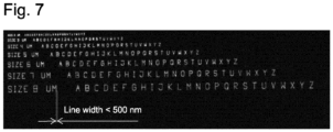
- a ceramic substrate having a size of 10 mm x 10 mm and consisting of 100 ⁇ m thick sapphire substrate (Al 2 O 3 ) was coated with a coating of CrN having a thickness of 100 nm by means of physical vapor deposition (PVD).
- PVD physical vapor deposition
- Circular recesses having a diameter of about 1 ⁇ m (Example 1) and approximately 500 nm (Examples 2 and 3) were ablated from the coating using a 200 femtosecond laser at a wavelength of 515 nm.
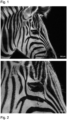
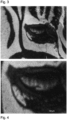
- Example 1 The resulting data carrier of Example 1 was imaged with an Olympus BX-51 at various magnifications.
- the respective transmission microscopy images at magnifications of 5x, 10x, 20x, 50x and 100x are shown in Figures 1-5 , respectively.
- the coating and ablation techniques illustrated above with reference to the examples may be analogously employed with a ceramic substrate having a thickness of at most 200 ⁇ m.
- the same coating may be applied onto the so-called glass-ribbon (reference number 2010-03E) available from Nippon Electric Glass. Said glass-ribbon is available in thicknesses between 4 ⁇ m and 50 ⁇ m and lengths of up to 100 m.
- Alumina Ribbon Ceramic or Ribbon ceramic made from zirconia both with a thickness as low as 20 ⁇ m, available from Corning, may be employed.
- AGC Spool AGC Dragontrail, Corning ® Willow ® Glass, Corning Standard Glass Carriers SGC 3.4, SGC 7.8 and SGC 9.0, Nippon Electric Glass - G-Leaf (Ultra-thin Glass), SCHOTT AS 87 eco, SCHOTT AF 32 Eco, and SCHOTT Xensation ® Flex.
Landscapes
- Engineering & Computer Science (AREA)
- Manufacturing & Machinery (AREA)
- Laser Beam Processing (AREA)
- Optical Record Carriers And Manufacture Thereof (AREA)
- Length Measuring Devices By Optical Means (AREA)
- Optical Recording Or Reproduction (AREA)
Claims (7)
- Verfahren zum Herstellen eines Datenträgers, wobei der Datenträger ein keramisches Substrat mit ersten und zweiten gegenüberliegenden Oberflächen und einer Dicke von höchstens 500 µm aufweist, wobei die erste Oberfläche des Substrats mit einer ersten Beschichtung beschichtet ist, wobei sich das Material der ersten Beschichtung von dem Material des keramischen Substrats unterscheidet, wobei die erste Beschichtung mehrere laserablatierte Vertiefungen aufweist, die Informationen codieren; wobei das Verfahren die folgenden Schritte aufweist:Bereitstellen eines keramischen Substrats;Beschichten der ersten Oberfläche des Substrats mit einer ersten Beschichtung durch physikalische Gasphasenabscheidung oder chemische Gasphasenabscheidung; undErzeugen von mehreren Vertiefungen in der ersten Beschichtung mittels Laserablation, wobei die laserablatierten Vertiefungen durch einen gepulsten Pikosekunden- oder Femtosekunden-Laser erzeugt werden;wobei der Datenträger nach dem Beschichtungsprozess bei einer Temperatur von mindestens 200°C getempert wird, um eine gesinterte Grenzfläche zwischen dem Substrat und der ersten Beschichtung zu erreichen, um die Verbindung zwischen dem Substrat und der ersten Beschichtung zu verbessern.
- Verfahren nach Anspruch 1, wobei die Dicke der ersten Beschichtung höchstens 10 µm, vorzugsweise höchstens 1 µm, besonders bevorzugt höchstens 100 nm, ganz besonders bevorzugt höchstens 50 nm beträgt.
- Verfahren nach einem der vorhergehenden Ansprüche, wobei jede Vertiefung in der ersten Beschichtung eine Tiefe von höchstens 10 µm, vorzugsweise höchstens 1 µm, besonders bevorzugt von höchstens 100 nm, ganz besonders bevorzugt von höchstens 50 nm aufweist.
- Verfahren nach einem der vorhergehenden Ansprüche, wobei jede Vertiefung in der ersten Beschichtung eine Tiefe aufweist, die kleiner ist als die Dicke der jeweiligen Beschichtung; oder wobei jede Vertiefung in der ersten Beschichtung eine Tiefe aufweist, die im Wesentlichen gleich der Dicke der jeweiligen Beschichtung ist; oder wobei jede Vertiefung in der ersten Beschichtung eine Tiefe aufweist, die größer ist als die Dicke der jeweiligen Beschichtung.
- Verfahren nach Anspruch 4, wobei sich jede Vertiefung mit einer Tiefe von höchstens 1 µm, vorzugsweise von höchstens 100 nm, besonders bevorzugt von höchstens 50 nm, in das Substrat erstreckt.
- Verfahren nach einem der vorhergehenden Ansprüche, wobei die erste Beschichtung eines oder eine Kombination der folgenden Materialien aufweist: ein Metall; ein Metallnitrid; ein Metallkarbid; ein Metalloxid; ein Metallborid; oder ein Metallsilizid.
- Verfahren nach einem der vorhergehenden Ansprüche, wobei das keramische Substrat für die Wellenlänge des für die Laserablation verwendeten Laserlichts transparent ist und wobei die Laserablation mit durch das keramische Substrat transmittiertem Laserlicht durchgeführt wird.
Priority Applications (1)
| Application Number | Priority Date | Filing Date | Title |
|---|---|---|---|
| EP24187596.2A EP4435784A3 (de) | 2021-02-12 | 2022-02-03 | Ultradünner datenträger und ausleseverfahren |
Applications Claiming Priority (3)
| Application Number | Priority Date | Filing Date | Title |
|---|---|---|---|
| EP21156858.9A EP4044182B1 (de) | 2021-02-12 | 2021-02-12 | Ultradünner datenträger |
| EP21210819 | 2021-11-26 | ||
| PCT/EP2022/052628 WO2022171522A1 (en) | 2021-02-12 | 2022-02-03 | Ultra-thin data carrier and method of read-out |
Related Child Applications (1)
| Application Number | Title | Priority Date | Filing Date |
|---|---|---|---|
| EP24187596.2A Division EP4435784A3 (de) | 2021-02-12 | 2022-02-03 | Ultradünner datenträger und ausleseverfahren |
Publications (3)
| Publication Number | Publication Date |
|---|---|
| EP4073794A1 EP4073794A1 (de) | 2022-10-19 |
| EP4073794C0 EP4073794C0 (de) | 2024-07-24 |
| EP4073794B1 true EP4073794B1 (de) | 2024-07-24 |
Family
ID=80625589
Family Applications (2)
| Application Number | Title | Priority Date | Filing Date |
|---|---|---|---|
| EP24187596.2A Pending EP4435784A3 (de) | 2021-02-12 | 2022-02-03 | Ultradünner datenträger und ausleseverfahren |
| EP22707349.1A Active EP4073794B1 (de) | 2021-02-12 | 2022-02-03 | Ultradünner datenträger |
Family Applications Before (1)
| Application Number | Title | Priority Date | Filing Date |
|---|---|---|---|
| EP24187596.2A Pending EP4435784A3 (de) | 2021-02-12 | 2022-02-03 | Ultradünner datenträger und ausleseverfahren |
Country Status (8)
| Country | Link |
|---|---|
| US (1) | US20240055021A1 (de) |
| EP (2) | EP4435784A3 (de) |
| JP (1) | JP2024508727A (de) |
| KR (1) | KR20230144543A (de) |
| DE (1) | DE202022003246U1 (de) |
| ES (1) | ES2985886T3 (de) |
| PL (1) | PL4073794T3 (de) |
| WO (1) | WO2022171522A1 (de) |
Families Citing this family (6)
| Publication number | Priority date | Publication date | Assignee | Title |
|---|---|---|---|---|
| WO2021028035A1 (en) * | 2019-08-14 | 2021-02-18 | Ceramic Data Solution GmbH | Method for long-term storage of information and storage medium therefor |
| CN115843362B (zh) | 2020-07-03 | 2025-07-04 | 陶瓷数据解决方案有限公司 | 用于长期存储信息的方法和信息存储介质的提高存储能力 |
| AU2021443312B2 (en) | 2021-04-29 | 2025-06-26 | Ceramic Data Solutions GmbH | Hybrid digital and analog data storage |
| ES3020085T3 (en) | 2021-05-17 | 2025-05-21 | Ceram Data Solutions Gmbh | High-speed reading by combining transmissive wide angle view with reflective focus view |
| US12431164B2 (en) | 2023-04-12 | 2025-09-30 | Corning Incorporated | Storage mediums and methods of making the same |
| WO2026019594A1 (en) | 2024-07-19 | 2026-01-22 | Boston Scientific Neuromodulation Corporation | Using stimulation circuitry to provide dc offset compensation in a stimulator device having tissue signal sensing capability |
Citations (6)
| Publication number | Priority date | Publication date | Assignee | Title |
|---|---|---|---|---|
| US4214249A (en) * | 1973-08-20 | 1980-07-22 | Canon Kabushiki Kaisha | Recording member for laser beam and process for recording |
| US20080320205A1 (en) * | 2006-11-27 | 2008-12-25 | Brigham Young University | Long-term digital data storage |
| US20100068444A1 (en) * | 2008-09-12 | 2010-03-18 | Asplund Matthew C | Data storage containing carbon and metal layers |
| US20110318695A1 (en) * | 2010-06-08 | 2011-12-29 | David Jen Hwang | Arbitrary pattern direct nanostructure fabrication methods and system |
| US20160118077A1 (en) * | 2014-10-23 | 2016-04-28 | Barry M. Lunt | Optical tape data storage |
| US20160199935A1 (en) * | 2015-01-12 | 2016-07-14 | The Chinese University Of Hong Kong | Parallel laser manufacturing system and method |
Family Cites Families (15)
| Publication number | Priority date | Publication date | Assignee | Title |
|---|---|---|---|---|
| LU86722A1 (fr) * | 1986-12-23 | 1988-07-14 | Glaverbel | Feuille en matiere vitreuse portant un dessin grave et procede pour graver un dessin sur un substrat en matiere vitreuse |
| JP2680591B2 (ja) * | 1988-02-15 | 1997-11-19 | シャープ株式会社 | 光メモリ素子の製造方法 |
| JPH02215587A (ja) * | 1989-02-17 | 1990-08-28 | Toshiba Corp | 光情報記録媒体 |
| JPH02277689A (ja) * | 1989-04-20 | 1990-11-14 | Toshiba Corp | 光情報記録媒体 |
| JPH08221808A (ja) * | 1995-02-20 | 1996-08-30 | Ricoh Co Ltd | 光ディスク原盤の製造方法 |
| JP4264517B2 (ja) * | 1997-10-24 | 2009-05-20 | 奇美電子股▲分▼有限公司 | レーザー記録媒体及び薄いガラス層を含むデータカード |
| US7666579B1 (en) * | 2001-09-17 | 2010-02-23 | Serenity Technologies, Inc. | Method and apparatus for high density storage of analog data in a durable medium |
| CN1839052B (zh) * | 2003-08-21 | 2011-09-07 | 三菱化学媒体股份有限公司 | 记录介质 |
| JP2007018649A (ja) * | 2005-07-11 | 2007-01-25 | Matsushita Electric Ind Co Ltd | 記録媒体用基板の製造方法 |
| JP5375698B2 (ja) * | 2010-03-23 | 2013-12-25 | コニカミノルタ株式会社 | ガラス基板の製造方法 |
| JP2013020660A (ja) * | 2011-07-07 | 2013-01-31 | Sony Corp | 光ディスク装置、位置制御方法 |
| WO2014097467A1 (ja) * | 2012-12-21 | 2014-06-26 | 株式会社日立製作所 | 光記録装置、光記録方法及び情報記録媒体 |
| US10719239B2 (en) | 2018-05-16 | 2020-07-21 | Microsoft Technology Licensing, Llc | Disaggregated data storage and retrieval system |
| WO2021028035A1 (en) | 2019-08-14 | 2021-02-18 | Ceramic Data Solution GmbH | Method for long-term storage of information and storage medium therefor |
| CN115843362B (zh) | 2020-07-03 | 2025-07-04 | 陶瓷数据解决方案有限公司 | 用于长期存储信息的方法和信息存储介质的提高存储能力 |
-
2022
- 2022-02-03 WO PCT/EP2022/052628 patent/WO2022171522A1/en not_active Ceased
- 2022-02-03 DE DE202022003246.3U patent/DE202022003246U1/de active Active
- 2022-02-03 US US18/264,732 patent/US20240055021A1/en active Pending
- 2022-02-03 PL PL22707349.1T patent/PL4073794T3/pl unknown
- 2022-02-03 JP JP2023548749A patent/JP2024508727A/ja active Pending
- 2022-02-03 ES ES22707349T patent/ES2985886T3/es active Active
- 2022-02-03 KR KR1020237027160A patent/KR20230144543A/ko active Pending
- 2022-02-03 EP EP24187596.2A patent/EP4435784A3/de active Pending
- 2022-02-03 EP EP22707349.1A patent/EP4073794B1/de active Active
Patent Citations (6)
| Publication number | Priority date | Publication date | Assignee | Title |
|---|---|---|---|---|
| US4214249A (en) * | 1973-08-20 | 1980-07-22 | Canon Kabushiki Kaisha | Recording member for laser beam and process for recording |
| US20080320205A1 (en) * | 2006-11-27 | 2008-12-25 | Brigham Young University | Long-term digital data storage |
| US20100068444A1 (en) * | 2008-09-12 | 2010-03-18 | Asplund Matthew C | Data storage containing carbon and metal layers |
| US20110318695A1 (en) * | 2010-06-08 | 2011-12-29 | David Jen Hwang | Arbitrary pattern direct nanostructure fabrication methods and system |
| US20160118077A1 (en) * | 2014-10-23 | 2016-04-28 | Barry M. Lunt | Optical tape data storage |
| US20160199935A1 (en) * | 2015-01-12 | 2016-07-14 | The Chinese University Of Hong Kong | Parallel laser manufacturing system and method |
Also Published As
| Publication number | Publication date |
|---|---|
| EP4435784A2 (de) | 2024-09-25 |
| EP4073794A1 (de) | 2022-10-19 |
| EP4073794C0 (de) | 2024-07-24 |
| ES2985886T3 (es) | 2024-11-07 |
| PL4073794T3 (pl) | 2024-11-04 |
| WO2022171522A1 (en) | 2022-08-18 |
| EP4435784A3 (de) | 2025-01-08 |
| DE202022003246U1 (de) | 2025-08-11 |
| KR20230144543A (ko) | 2023-10-16 |
| JP2024508727A (ja) | 2024-02-28 |
| US20240055021A1 (en) | 2024-02-15 |
Similar Documents
| Publication | Publication Date | Title |
|---|---|---|
| EP4073794B1 (de) | Ultradünner datenträger | |
| EP4044182B1 (de) | Ultradünner datenträger | |
| AU2020456046B2 (en) | Increased storage capacity for a method for long-term storage of information and storage medium therefor | |
| EP3779987B1 (de) | Verfahren zur langzeitspeicherung von informationen und speichermedium dafür | |
| US6839173B2 (en) | Reflection type diffraction grating | |
| EP2962137B1 (de) | Verbesserte dauerhafte silberbeschichtungen für hochreflektive spiegel | |
| JP4895902B2 (ja) | 反射膜の形成方法 | |
| JP7587801B2 (ja) | 耐久性向上のためナノラミネートを備えた光学コーティング | |
| EP4198979A1 (de) | Ultradünner datenträger und verfahren zum auslesen | |
| US20250021781A1 (en) | Ultra-Thin Data Carrier and Method of Read-Out | |
| TWI249164B (en) | Optical recording medium | |
| CN116964672A (zh) | 超薄数据载体及其读出方法 | |
| CN118696376A (zh) | 超薄数据载体和读出方法 | |
| JP4443958B2 (ja) | 鏡およびその製造方法 | |
| RU2786371C1 (ru) | Способ долговременного хранения информации и носитель для этого | |
| US20190064398A1 (en) | Durable silver-based mirror coating employing nickel oxide |
Legal Events
| Date | Code | Title | Description |
|---|---|---|---|
| STAA | Information on the status of an ep patent application or granted ep patent |
Free format text: STATUS: UNKNOWN |
|
| STAA | Information on the status of an ep patent application or granted ep patent |
Free format text: STATUS: THE INTERNATIONAL PUBLICATION HAS BEEN MADE |
|
| PUAI | Public reference made under article 153(3) epc to a published international application that has entered the european phase |
Free format text: ORIGINAL CODE: 0009012 |
|
| STAA | Information on the status of an ep patent application or granted ep patent |
Free format text: STATUS: REQUEST FOR EXAMINATION WAS MADE |
|
| 17P | Request for examination filed |
Effective date: 20220712 |
|
| AK | Designated contracting states |
Kind code of ref document: A1 Designated state(s): AL AT BE BG CH CY CZ DE DK EE ES FI FR GB GR HR HU IE IS IT LI LT LU LV MC MK MT NL NO PL PT RO RS SE SI SK SM TR |
|
| STAA | Information on the status of an ep patent application or granted ep patent |
Free format text: STATUS: EXAMINATION IS IN PROGRESS |
|
| 17Q | First examination report despatched |
Effective date: 20221107 |
|
| GRAP | Despatch of communication of intention to grant a patent |
Free format text: ORIGINAL CODE: EPIDOSNIGR1 |
|
| STAA | Information on the status of an ep patent application or granted ep patent |
Free format text: STATUS: GRANT OF PATENT IS INTENDED |
|
| DAV | Request for validation of the european patent (deleted) | ||
| DAX | Request for extension of the european patent (deleted) | ||
| INTG | Intention to grant announced |
Effective date: 20240221 |
|
| GRAS | Grant fee paid |
Free format text: ORIGINAL CODE: EPIDOSNIGR3 |
|
| GRAA | (expected) grant |
Free format text: ORIGINAL CODE: 0009210 |
|
| STAA | Information on the status of an ep patent application or granted ep patent |
Free format text: STATUS: THE PATENT HAS BEEN GRANTED |
|
| AK | Designated contracting states |
Kind code of ref document: B1 Designated state(s): AL AT BE BG CH CY CZ DE DK EE ES FI FR GB GR HR HU IE IS IT LI LT LU LV MC MK MT NL NO PL PT RO RS SE SI SK SM TR |
|
| REG | Reference to a national code |
Ref country code: GB Ref legal event code: FG4D |
|
| REG | Reference to a national code |
Ref country code: CH Ref legal event code: EP |
|
| REG | Reference to a national code |
Ref country code: DE Ref legal event code: R096 Ref document number: 602022004845 Country of ref document: DE |
|
| REG | Reference to a national code |
Ref country code: IE Ref legal event code: FG4D |
|
| U01 | Request for unitary effect filed |
Effective date: 20240724 |
|
| U07 | Unitary effect registered |
Designated state(s): AT BE BG DE DK EE FI FR IT LT LU LV MT NL PT SE SI Effective date: 20240731 |
|
| REG | Reference to a national code |
Ref country code: ES Ref legal event code: FG2A Ref document number: 2985886 Country of ref document: ES Kind code of ref document: T3 Effective date: 20241107 |
|
| PG25 | Lapsed in a contracting state [announced via postgrant information from national office to epo] |
Ref country code: NO Free format text: LAPSE BECAUSE OF FAILURE TO SUBMIT A TRANSLATION OF THE DESCRIPTION OR TO PAY THE FEE WITHIN THE PRESCRIBED TIME-LIMIT Effective date: 20241024 |
|
| PG25 | Lapsed in a contracting state [announced via postgrant information from national office to epo] |
Ref country code: GR Free format text: LAPSE BECAUSE OF FAILURE TO SUBMIT A TRANSLATION OF THE DESCRIPTION OR TO PAY THE FEE WITHIN THE PRESCRIBED TIME-LIMIT Effective date: 20241025 |
|
| PG25 | Lapsed in a contracting state [announced via postgrant information from national office to epo] |
Ref country code: IS Free format text: LAPSE BECAUSE OF FAILURE TO SUBMIT A TRANSLATION OF THE DESCRIPTION OR TO PAY THE FEE WITHIN THE PRESCRIBED TIME-LIMIT Effective date: 20241124 |
|
| PG25 | Lapsed in a contracting state [announced via postgrant information from national office to epo] |
Ref country code: HR Free format text: LAPSE BECAUSE OF FAILURE TO SUBMIT A TRANSLATION OF THE DESCRIPTION OR TO PAY THE FEE WITHIN THE PRESCRIBED TIME-LIMIT Effective date: 20240724 |
|
| PG25 | Lapsed in a contracting state [announced via postgrant information from national office to epo] |
Ref country code: RS Free format text: LAPSE BECAUSE OF FAILURE TO SUBMIT A TRANSLATION OF THE DESCRIPTION OR TO PAY THE FEE WITHIN THE PRESCRIBED TIME-LIMIT Effective date: 20241024 |
|
| PG25 | Lapsed in a contracting state [announced via postgrant information from national office to epo] |
Ref country code: RS Free format text: LAPSE BECAUSE OF FAILURE TO SUBMIT A TRANSLATION OF THE DESCRIPTION OR TO PAY THE FEE WITHIN THE PRESCRIBED TIME-LIMIT Effective date: 20241024 Ref country code: NO Free format text: LAPSE BECAUSE OF FAILURE TO SUBMIT A TRANSLATION OF THE DESCRIPTION OR TO PAY THE FEE WITHIN THE PRESCRIBED TIME-LIMIT Effective date: 20241024 Ref country code: IS Free format text: LAPSE BECAUSE OF FAILURE TO SUBMIT A TRANSLATION OF THE DESCRIPTION OR TO PAY THE FEE WITHIN THE PRESCRIBED TIME-LIMIT Effective date: 20241124 Ref country code: HR Free format text: LAPSE BECAUSE OF FAILURE TO SUBMIT A TRANSLATION OF THE DESCRIPTION OR TO PAY THE FEE WITHIN THE PRESCRIBED TIME-LIMIT Effective date: 20240724 Ref country code: GR Free format text: LAPSE BECAUSE OF FAILURE TO SUBMIT A TRANSLATION OF THE DESCRIPTION OR TO PAY THE FEE WITHIN THE PRESCRIBED TIME-LIMIT Effective date: 20241025 |
|
| U20 | Renewal fee for the european patent with unitary effect paid |
Year of fee payment: 4 Effective date: 20250226 |
|
| PG25 | Lapsed in a contracting state [announced via postgrant information from national office to epo] |
Ref country code: RO Free format text: LAPSE BECAUSE OF FAILURE TO SUBMIT A TRANSLATION OF THE DESCRIPTION OR TO PAY THE FEE WITHIN THE PRESCRIBED TIME-LIMIT Effective date: 20240724 Ref country code: SM Free format text: LAPSE BECAUSE OF FAILURE TO SUBMIT A TRANSLATION OF THE DESCRIPTION OR TO PAY THE FEE WITHIN THE PRESCRIBED TIME-LIMIT Effective date: 20240724 |
|
| PG25 | Lapsed in a contracting state [announced via postgrant information from national office to epo] |
Ref country code: CZ Free format text: LAPSE BECAUSE OF FAILURE TO SUBMIT A TRANSLATION OF THE DESCRIPTION OR TO PAY THE FEE WITHIN THE PRESCRIBED TIME-LIMIT Effective date: 20240724 |
|
| PGFP | Annual fee paid to national office [announced via postgrant information from national office to epo] |
Ref country code: PL Payment date: 20250129 Year of fee payment: 4 |
|
| PG25 | Lapsed in a contracting state [announced via postgrant information from national office to epo] |
Ref country code: SK Free format text: LAPSE BECAUSE OF FAILURE TO SUBMIT A TRANSLATION OF THE DESCRIPTION OR TO PAY THE FEE WITHIN THE PRESCRIBED TIME-LIMIT Effective date: 20240724 |
|
| PLBE | No opposition filed within time limit |
Free format text: ORIGINAL CODE: 0009261 |
|
| STAA | Information on the status of an ep patent application or granted ep patent |
Free format text: STATUS: NO OPPOSITION FILED WITHIN TIME LIMIT |
|
| 26N | No opposition filed |
Effective date: 20250425 |
|
| PG25 | Lapsed in a contracting state [announced via postgrant information from national office to epo] |
Ref country code: MC Free format text: LAPSE BECAUSE OF FAILURE TO SUBMIT A TRANSLATION OF THE DESCRIPTION OR TO PAY THE FEE WITHIN THE PRESCRIBED TIME-LIMIT Effective date: 20240724 |
|
| REG | Reference to a national code |
Ref country code: CH Ref legal event code: PL |
|
| PG25 | Lapsed in a contracting state [announced via postgrant information from national office to epo] |
Ref country code: CH Free format text: LAPSE BECAUSE OF NON-PAYMENT OF DUE FEES Effective date: 20250228 |
|
| U20 | Renewal fee for the european patent with unitary effect paid |
Year of fee payment: 5 Effective date: 20260225 |
|
| PGFP | Annual fee paid to national office [announced via postgrant information from national office to epo] |
Ref country code: GB Payment date: 20260226 Year of fee payment: 5 |
|
| PGFP | Annual fee paid to national office [announced via postgrant information from national office to epo] |
Ref country code: ES Payment date: 20260317 Year of fee payment: 5 |
|
| PGFP | Annual fee paid to national office [announced via postgrant information from national office to epo] |
Ref country code: IE Payment date: 20260219 Year of fee payment: 5 |