EP4073008B1 - Pasten für solarzellen, solarzellen und verfahren zum herstellen derselben - Google Patents
Pasten für solarzellen, solarzellen und verfahren zum herstellen derselben Download PDFInfo
- Publication number
- EP4073008B1 EP4073008B1 EP20845247.4A EP20845247A EP4073008B1 EP 4073008 B1 EP4073008 B1 EP 4073008B1 EP 20845247 A EP20845247 A EP 20845247A EP 4073008 B1 EP4073008 B1 EP 4073008B1
- Authority
- EP
- European Patent Office
- Prior art keywords
- paste
- copper
- particles
- oxide
- nanoparticles
- Prior art date
- Legal status (The legal status is an assumption and is not a legal conclusion. Google has not performed a legal analysis and makes no representation as to the accuracy of the status listed.)
- Active
Links
Images


Classifications
-
- H—ELECTRICITY
- H01—ELECTRIC ELEMENTS
- H01B—CABLES; CONDUCTORS; INSULATORS; SELECTION OF MATERIALS FOR THEIR CONDUCTIVE, INSULATING OR DIELECTRIC PROPERTIES
- H01B1/00—Conductors or conductive bodies characterised by the conductive materials; Selection of materials as conductors
- H01B1/20—Conductive material dispersed in non-conductive organic material
-
- H—ELECTRICITY
- H10—SEMICONDUCTOR DEVICES; ELECTRIC SOLID-STATE DEVICES NOT OTHERWISE PROVIDED FOR
- H10F—INORGANIC SEMICONDUCTOR DEVICES SENSITIVE TO INFRARED RADIATION, LIGHT, ELECTROMAGNETIC RADIATION OF SHORTER WAVELENGTH OR CORPUSCULAR RADIATION
- H10F19/00—Integrated devices, or assemblies of multiple devices, comprising at least one photovoltaic cell covered by group H10F10/00, e.g. photovoltaic modules
- H10F19/90—Structures for connecting between photovoltaic cells, e.g. interconnections or insulating spacers
- H10F19/902—Structures for connecting between photovoltaic cells, e.g. interconnections or insulating spacers for series or parallel connection of photovoltaic cells
- H10F19/906—Structures for connecting between photovoltaic cells, e.g. interconnections or insulating spacers for series or parallel connection of photovoltaic cells characterised by the materials of the structures
-
- C—CHEMISTRY; METALLURGY
- C03—GLASS; MINERAL OR SLAG WOOL
- C03C—CHEMICAL COMPOSITION OF GLASSES, GLAZES OR VITREOUS ENAMELS; SURFACE TREATMENT OF GLASS; SURFACE TREATMENT OF FIBRES OR FILAMENTS MADE FROM GLASS, MINERALS OR SLAGS; JOINING GLASS TO GLASS OR OTHER MATERIALS
- C03C8/00—Enamels; Glazes; Fusion seal compositions being frit compositions having non-frit additions
- C03C8/02—Frit compositions, i.e. in a powdered or comminuted form
- C03C8/10—Frit compositions, i.e. in a powdered or comminuted form containing lead
-
- C—CHEMISTRY; METALLURGY
- C03—GLASS; MINERAL OR SLAG WOOL
- C03C—CHEMICAL COMPOSITION OF GLASSES, GLAZES OR VITREOUS ENAMELS; SURFACE TREATMENT OF GLASS; SURFACE TREATMENT OF FIBRES OR FILAMENTS MADE FROM GLASS, MINERALS OR SLAGS; JOINING GLASS TO GLASS OR OTHER MATERIALS
- C03C8/00—Enamels; Glazes; Fusion seal compositions being frit compositions having non-frit additions
- C03C8/14—Glass frit mixtures having non-frit additions, e.g. opacifiers, colorants, mill-additions
- C03C8/18—Glass frit mixtures having non-frit additions, e.g. opacifiers, colorants, mill-additions containing free metals
-
- C—CHEMISTRY; METALLURGY
- C03—GLASS; MINERAL OR SLAG WOOL
- C03C—CHEMICAL COMPOSITION OF GLASSES, GLAZES OR VITREOUS ENAMELS; SURFACE TREATMENT OF GLASS; SURFACE TREATMENT OF FIBRES OR FILAMENTS MADE FROM GLASS, MINERALS OR SLAGS; JOINING GLASS TO GLASS OR OTHER MATERIALS
- C03C8/00—Enamels; Glazes; Fusion seal compositions being frit compositions having non-frit additions
- C03C8/22—Enamels; Glazes; Fusion seal compositions being frit compositions having non-frit additions containing two or more distinct frits having different compositions
-
- C—CHEMISTRY; METALLURGY
- C08—ORGANIC MACROMOLECULAR COMPOUNDS; THEIR PREPARATION OR CHEMICAL WORKING-UP; COMPOSITIONS BASED THEREON
- C08K—Use of inorganic or non-macromolecular organic substances as compounding ingredients
- C08K3/00—Use of inorganic substances as compounding ingredients
- C08K3/02—Elements
- C08K3/08—Metals
-
- C—CHEMISTRY; METALLURGY
- C08—ORGANIC MACROMOLECULAR COMPOUNDS; THEIR PREPARATION OR CHEMICAL WORKING-UP; COMPOSITIONS BASED THEREON
- C08K—Use of inorganic or non-macromolecular organic substances as compounding ingredients
- C08K3/00—Use of inorganic substances as compounding ingredients
- C08K3/18—Oxygen-containing compounds, e.g. metal carbonyls
- C08K3/20—Oxides; Hydroxides
- C08K3/22—Oxides; Hydroxides of metals
- C08K3/2279—Oxides; Hydroxides of metals of antimony
-
- C—CHEMISTRY; METALLURGY
- C08—ORGANIC MACROMOLECULAR COMPOUNDS; THEIR PREPARATION OR CHEMICAL WORKING-UP; COMPOSITIONS BASED THEREON
- C08K—Use of inorganic or non-macromolecular organic substances as compounding ingredients
- C08K9/00—Use of pretreated ingredients
- C08K9/02—Ingredients treated with inorganic substances
-
- C—CHEMISTRY; METALLURGY
- C08—ORGANIC MACROMOLECULAR COMPOUNDS; THEIR PREPARATION OR CHEMICAL WORKING-UP; COMPOSITIONS BASED THEREON
- C08L—COMPOSITIONS OF MACROMOLECULAR COMPOUNDS
- C08L39/00—Compositions of homopolymers or copolymers of compounds having one or more unsaturated aliphatic radicals, each having only one carbon-to-carbon double bond, and at least one being terminated by a single or double bond to nitrogen or by a heterocyclic ring containing nitrogen; Compositions of derivatives of such polymers
- C08L39/04—Homopolymers or copolymers of monomers containing heterocyclic rings having nitrogen as ring member
- C08L39/06—Homopolymers or copolymers of N-vinyl-pyrrolidones
-
- C—CHEMISTRY; METALLURGY
- C09—DYES; PAINTS; POLISHES; NATURAL RESINS; ADHESIVES; COMPOSITIONS NOT OTHERWISE PROVIDED FOR; APPLICATIONS OF MATERIALS NOT OTHERWISE PROVIDED FOR
- C09D—COATING COMPOSITIONS, e.g. PAINTS, VARNISHES OR LACQUERS; FILLING PASTES; CHEMICAL PAINT OR INK REMOVERS; INKS; CORRECTING FLUIDS; WOODSTAINS; PASTES OR SOLIDS FOR COLOURING OR PRINTING; USE OF MATERIALS THEREFOR
- C09D11/00—Inks
- C09D11/02—Printing inks
- C09D11/03—Printing inks characterised by features other than the chemical nature of the binder
- C09D11/037—Printing inks characterised by features other than the chemical nature of the binder characterised by the pigment
-
- C—CHEMISTRY; METALLURGY
- C09—DYES; PAINTS; POLISHES; NATURAL RESINS; ADHESIVES; COMPOSITIONS NOT OTHERWISE PROVIDED FOR; APPLICATIONS OF MATERIALS NOT OTHERWISE PROVIDED FOR
- C09D—COATING COMPOSITIONS, e.g. PAINTS, VARNISHES OR LACQUERS; FILLING PASTES; CHEMICAL PAINT OR INK REMOVERS; INKS; CORRECTING FLUIDS; WOODSTAINS; PASTES OR SOLIDS FOR COLOURING OR PRINTING; USE OF MATERIALS THEREFOR
- C09D11/00—Inks
- C09D11/52—Electrically conductive inks
-
- H—ELECTRICITY
- H01—ELECTRIC ELEMENTS
- H01B—CABLES; CONDUCTORS; INSULATORS; SELECTION OF MATERIALS FOR THEIR CONDUCTIVE, INSULATING OR DIELECTRIC PROPERTIES
- H01B1/00—Conductors or conductive bodies characterised by the conductive materials; Selection of materials as conductors
- H01B1/20—Conductive material dispersed in non-conductive organic material
- H01B1/22—Conductive material dispersed in non-conductive organic material the conductive material comprising metals or alloys
-
- H—ELECTRICITY
- H01—ELECTRIC ELEMENTS
- H01B—CABLES; CONDUCTORS; INSULATORS; SELECTION OF MATERIALS FOR THEIR CONDUCTIVE, INSULATING OR DIELECTRIC PROPERTIES
- H01B13/00—Apparatus or processes specially adapted for manufacturing conductors or cables
-
- H—ELECTRICITY
- H01—ELECTRIC ELEMENTS
- H01L—SEMICONDUCTOR DEVICES NOT COVERED BY CLASS H10
- H01L21/00—Processes or apparatus adapted for the manufacture or treatment of semiconductor or solid state devices or of parts thereof
- H01L21/02—Manufacture or treatment of semiconductor devices or of parts thereof
- H01L21/04—Manufacture or treatment of semiconductor devices or of parts thereof the devices having potential barriers, e.g. a PN junction, depletion layer or carrier concentration layer
- H01L21/48—Manufacture or treatment of parts, e.g. containers, prior to assembly of the devices, using processes not provided for in a single one of the groups H01L21/18 - H01L21/326 or H10D48/04 - H10D48/07
- H01L21/4814—Conductive parts
- H01L21/4846—Leads on or in insulating or insulated substrates, e.g. metallisation
- H01L21/4867—Applying pastes or inks, e.g. screen printing
-
- H—ELECTRICITY
- H10—SEMICONDUCTOR DEVICES; ELECTRIC SOLID-STATE DEVICES NOT OTHERWISE PROVIDED FOR
- H10F—INORGANIC SEMICONDUCTOR DEVICES SENSITIVE TO INFRARED RADIATION, LIGHT, ELECTROMAGNETIC RADIATION OF SHORTER WAVELENGTH OR CORPUSCULAR RADIATION
- H10F77/00—Constructional details of devices covered by this subclass
- H10F77/20—Electrodes
- H10F77/206—Electrodes for devices having potential barriers
- H10F77/211—Electrodes for devices having potential barriers for photovoltaic cells
- H10F77/219—Arrangements for electrodes of back-contact photovoltaic cells
- H10F77/223—Arrangements for electrodes of back-contact photovoltaic cells for metallisation wrap-through [MWT] photovoltaic cells
-
- C—CHEMISTRY; METALLURGY
- C08—ORGANIC MACROMOLECULAR COMPOUNDS; THEIR PREPARATION OR CHEMICAL WORKING-UP; COMPOSITIONS BASED THEREON
- C08K—Use of inorganic or non-macromolecular organic substances as compounding ingredients
- C08K3/00—Use of inorganic substances as compounding ingredients
- C08K3/02—Elements
- C08K3/08—Metals
- C08K2003/085—Copper
-
- C—CHEMISTRY; METALLURGY
- C08—ORGANIC MACROMOLECULAR COMPOUNDS; THEIR PREPARATION OR CHEMICAL WORKING-UP; COMPOSITIONS BASED THEREON
- C08K—Use of inorganic or non-macromolecular organic substances as compounding ingredients
- C08K2201/00—Specific properties of additives
- C08K2201/002—Physical properties
- C08K2201/005—Additives being defined by their particle size in general
-
- Y—GENERAL TAGGING OF NEW TECHNOLOGICAL DEVELOPMENTS; GENERAL TAGGING OF CROSS-SECTIONAL TECHNOLOGIES SPANNING OVER SEVERAL SECTIONS OF THE IPC; TECHNICAL SUBJECTS COVERED BY FORMER USPC CROSS-REFERENCE ART COLLECTIONS [XRACs] AND DIGESTS
- Y02—TECHNOLOGIES OR APPLICATIONS FOR MITIGATION OR ADAPTATION AGAINST CLIMATE CHANGE
- Y02E—REDUCTION OF GREENHOUSE GAS [GHG] EMISSIONS, RELATED TO ENERGY GENERATION, TRANSMISSION OR DISTRIBUTION
- Y02E10/00—Energy generation through renewable energy sources
- Y02E10/50—Photovoltaic [PV] energy
Definitions
- the present invention relates generally to the manufacturing of solar panels and to paste compositions for use during the manufacturing of components of solar panels, and more particularly to metal-containing pastes, solar cells made with those pastes, and the methods of making and using those pastes in solar panel manufacturing.
- a solar panel While being made primarily of silicon, a solar panel has numerous other structures by which sunlight is converted into electricity.
- a solar panel is composed of solar cells that are typically connected in series using tabbing wires/ribbons and are hermetically encapsulated between a glass front sheet and a back sheet.
- Each solar cell includes a silicon wafer that is doped to produce a p-n junction. When exposed to sunlight, the electric field at the p-n junction separates charge carriers (i.e., electrons and holes). In this way, electrical current is produced.
- Other structures of a solar panel can include an antireflective coating (e.g., silicon nitride (SiN) and titanium dioxide (TiO 2 )) on the front side or sun-exposed side of the doped silicon wafer.
- the coating reduces light reflection from the cell and thus improves the efficiency of the cell.
- Charge carriers produced during light exposure are collected by conductive contacts on the front side and back side of each cell.
- the conductive contacts are typically positioned across the front side in lines 15 ⁇ m to 200 ⁇ m wide and spaced every 0.7 mm to 5 mm apart. Each line may be referred to as a "finger.” The spacing and individual widths of the fingers permit sunlight to impinge upon large surface areas of the doped silicon.
- the conductive contact on the backside does not need to be transparent. Often a thin layer of metal, such as aluminum, forms the back side of the cell. Additional conductive connections, such as bus bars, which are 0.1 mm to 2 mm wide and made of silver, are electrically coupled to the fingers and backside aluminum. While not limited to any particular number, the number of bus bars can range from 2 to 8 and may be replaced with other configurations and even non-busbar designs.
- the fingers and bus bars on current silicon solar cells are nearly all silver (Ag). With the increased demand and plummeting margins, manufacturers have minimized silver use. That minimization has been accomplished through improvements to the paste formulation and optimization of the paste-printing process.
- One method of reducing cost is to reduce the width of each finger of silver. This alone has resulted in a 50% reduction in silver consumption. While additional reductions are possible, there is a lower limit, below which both device performance and production yields become unacceptable. As manufacturers push the lower limit on silver use to reduce costs, less expensive alternatives to silver are being investigated.
- Copper is an ideal alternative to silver. Copper is significantly cheaper while having comparable electrical conductivity.
- One downside is that copper degrades a solar cell quickly, and so the use of copper complicates manufacturing.
- One technique is electroplating. While generally successful, electroplating requires newer equipment and added processing beyond current silver-paste screen-printing techniques. Because significant capital investment is required to utilize electroplating of copper, it has not been adopted by industry. There are additional disadvantages.
- Electroplated copper requires application of a diffusion barrier on the silicon prior to the deposition of copper. The copper is then electroplated over that barrier. The diffusion barrier thus separates the copper from the silicon. During use of the solar cell, the copper is prohibited by the barrier from diffusing into the silicon. Another issue is, unlike silver, copper readily oxidizes.
- CN 100 700 428 A discloses a paste for solar cell based on copper-metal powder.
- the present invention overcomes the foregoing and other shortcomings and drawbacks of solar panels, pastes, and methods for manufacturing same. While the invention will be described in connection with certain embodiments, it will be understood that the invention is not limited to these embodiments. On the contrary, the invention includes all alternatives, modifications and equivalents as may be included within the scope of the present invention.
- a method of making a solar cell according to appended claim 15 According to a third aspect of the invention there is provided a solar cell according to appended claim 16.
- a paste for use in metallization of a solar cell comprises an organic vehicle including polyvinylpyrrolidone, and a mixture of copper-containing particles, metal-oxide-containing nanoparticles, and secondary oxide particles different from the metal-oxide-containing nanoparticles in the organic vehicle.
- the secondary oxide particles include particles of a metal oxide, and a metal of the metal oxide capable of reducing at least some of the metal-oxide-containing nanoparticles to metal when the paste is heated to a temperature at which the organic vehicle decomposes.
- the nanoparticles are each a discrete particle where all three dimensions are equal to or less than 100 nm
- the organic vehicle is capable of reducing the metal oxide of the secondary oxide particles upon decomposition of the organic vehicle.
- the organic vehicle includes polyvinylpyrrolidone.
- the secondary oxide particles include frit particles.
- the copper-containing particles include metallic copper particles or copper alloy particles.
- the metallic copper particles have at least one metal of nickel, cobalt, or manganese on the surfaces of the metallic copper particles or on the surfaces of the copper alloy particles.
- the at least one metal of nickel, cobalt, or manganese is in the form of a metallic particle on the surfaces of the metallic copper particles or on the surfaces of the copper alloy particles.
- the at least one metal of nickel, cobalt, or manganese is in the form of a metal oxide particle on the surfaces of the metallic copper particles or on the surfaces of the copper alloy particles.
- the metallic copper particles or the copper alloy particles and/or the at least one metal are doped with at least phosphorous.
- the surfaces of the metallic copper particles or the surfaces of the copper alloy particles are not fully covered by the at least one metal.
- the at least one metal covers at least a portion of the surfaces of the metallic copper particles or covers at least a portion of the surfaces of the copper alloy particles.
- the metal oxide of the secondary oxide particles is antimony oxide.
- the metal-oxide containing nanoparticles include at least one oxide of nickel, copper, cobalt, manganese, and lead.
- the metal-oxide-containing nanoparticles include oxides of nickel and lead.
- the metal oxide of the secondary oxide particles includes antimony oxide.
- the metal-oxide-containing nanoparticles include oxides of nickel, copper, and lead.
- the paste is free of silver.
- a ratio of secondary oxide particles to metal-oxide-containing nanoparticles is in a range of 0.50 to 16.96 by weight.
- a ratio of secondary oxide particles to metal-oxide-containing nanoparticles is in a range of 1.50 to 3.51 by weight.
- the at least one metal of nickel, cobalt, and manganese is in the form of a metallic particle on the surfaces of the copper-containing particles and the copper-containing particles with metallic particles have a surface area in the range of 1 m 2 /g to 5 m 2 /g.
- the at least one metal of nickel, cobalt, and manganese is in the form of a metallic particle on the surfaces of the copper-containing particles and the copper-containing particles with metallic particles have a surface area in the range of 0.7 m 2 /g to 5 m 2 /g.
- the copper-containing particles include a mixture of a fine copper powder and a coarse copper powder.
- the fine copper powder is characterized by an average particle size in a range of 1.2 ⁇ m to 3.2 ⁇ m and the coarse copper powder is characterized by an average particle size in a range of 7.53 ⁇ m to 14.69 ⁇ m, 10 ⁇ m to 20 ⁇ m or 1.75 ⁇ m to 7.20 ⁇ m.
- the organic vehicle is an organic binder and an organic solvent.
- the organic vehicle further includes a viscosity modifier.
- the organic solvent is propylene glycol.
- the organic vehicle further includes an organic binder.
- a paste comprises an organic vehicle, and a mixture of particles including metallic copper particles, nanoparticles, and metal oxide particles in the organic vehicle.
- the nanoparticles include at least one oxide of nickel, copper, cobalt, manganese, antimony, tellurium, bismuth, and lead.
- the metal oxide of the metal oxide particles has a more negative Gibbs Free Energy of Formation than a metal oxide of the at least one oxide of the nanoparticles.
- the metallic copper particles form the largest volume portion of metal in the paste.
- nanoparticles include lead oxide containing particles.
- nanoparticles are oxides of nickel and lead.
- the metal oxide particles include particles of antimony oxide.
- the nanoparticles include lead oxide containing particles and the metal oxide particles include particles of antimony oxide.
- the organic vehicle is capable of reducing the metal oxide particles upon decomposition of the organic vehicle.
- organic vehicle includes polyvinylpyrrolidone.
- the metal oxide particles include frit particles.
- the metallic copper particles have at least one metal of nickel, cobalt, or manganese on the surfaces of the metallic copper particles.
- the at least one metal of nickel, cobalt, or manganese is in the form of a metallic particle on the surfaces of the metallic copper particles.
- the at least one metal of nickel, cobalt, or manganese is in the form of a metal oxide particle on the surfaces of the metallic copper particles.
- the metallic copper particles and/or the at least one metal are doped with at least phosphorous.
- the surfaces of the metallic copper particles are not fully covered by the at least one metal.
- the at least one metal covers at least a portion of the surfaces of the metallic copper particles.
- the metal oxide particles are particles of antimony oxide.
- nanoparticles include at least one oxide of nickel, copper, cobalt, manganese, and lead.
- nanoparticles include oxides of nickel and lead.
- the metal oxide particles are particles of antimony oxide.
- nanoparticles include oxides of nickel, copper, and lead.
- the paste is free of silver.
- a ratio of metal oxide particles to nanoparticles is in a range of 0.5 to 17 by weight.
- a ratio of metal oxide particles to nanoparticles is in a range of 1.5 to 3.5 by weight.
- a ratio of metal oxide particles to nanoparticles is in a range of 0.25 to 20 by weight.
- a ratio of metal oxide particles to nanoparticles is in a range of 3 to 17 by weight.
- the nanoparticles include lead oxide and/or lead hydroxide containing particles and the metal oxide particles include particles of antimony oxide.
- the metallic copper particles are modified to include metal-containing particles on their surfaces.
- modified metallic copper particles have a surface area greater than a surface area of the metallic copper particles without modification.
- the modified metallic copper particles have a surface area in the range of 0.7 m 2 /g to 5 m 2 /g.
- the modified metallic copper particles have a surface area in the range of 1 m 2 /g to 5 m 2 /g.
- the metallic copper particles include a mixture of a fine copper powder and a coarse copper powder.
- the fine copper powder is characterized by an average particle size in a range of 1.2 ⁇ m to 3.2 ⁇ m and the coarse copper powder is characterized by an average particle size in a range of 7.53 ⁇ m to 14.69 ⁇ m, 10 ⁇ m to 20 ⁇ m, or 1.75 ⁇ m to 7.20 ⁇ m.
- the organic vehicle is an organic binder and an organic solvent.
- organic vehicle further includes a viscosity modifier.
- organic solvent is propylene glycol.
- vehicle further includes an organic binder.
- organic solvent is one of propylene glycol, dipropylene glycol, and tripropylene glycol, or combinations thereof.
- the metallic copper particles consist of a fine copper powder.
- the fine copper powder is characterized by an average particle size in a range of 1.2 ⁇ m to 3.2 ⁇ m.
- a paste consists essentially of an organic vehicle, and a mixture of metallic copper particles, nanoparticles, and metal oxide particles in the organic vehicle.
- the nanoparticles include at least one oxide of nickel, copper, cobalt, manganese, antimony, tellurium, bismuth, and lead.
- a paste consists of an organic vehicle and a mixture of metallic copper particles, nanoparticles, and metal oxide particles in the organic vehicle.
- the nanoparticles include at least one oxide of nickel, copper, cobalt, manganese, antimony, tellurium, bismuth, and lead.
- a solar cell comprises a semiconductor substrate and at least one copper-containing conductor on the semiconductor substrate.
- the copper-containing conductor includes a plurality of grains of copper or a copper alloy and at least portions of grain boundaries between adjacent grains include at least one of lead, copper, cobalt, manganese, tellurium, and bismuth and at least one other metal.
- an oxide of at least one other metal has a more negative Gibbs Free Energy of Formation than lead oxide.
- the at least one other metal is antimony.
- At least portions of the grain boundaries further include nickel.
- the copper-containing conductor and the semiconductor substrate meet at an interface and the interface includes lead and the at least one other metal between the semiconductor substrate and the grains.
- the interface further includes nickel.
- the solar cell is free of silver.
- the copper-containing conductor is a finger.
- the finger has a thickness in the range of 10 ⁇ m to 100 ⁇ m.
- the solar cell includes a highly doped silicon emitter layer, and the finger is in electrical contact with the silicon emitter layer.
- the finger has a resistivity that is in the range of 2 times to 10 times the resistivity of bulk metallic copper.
- the conductor is a busbar.
- busbar has a thickness in the range of 10 ⁇ m to 100 ⁇ m.
- the solar cell includes an anti-reflective layer on the semiconductor substrate, the anti-reflective layer defines an outer surface of the solar cell, and the busbar is in direct contact with the anti-reflective layer but does not contact the semiconductor substrate.
- the solar cell further includes a plurality of the busbars arranged in a pattern in which the busbars are spaced apart by a distance of less than 40 mm.
- the solar cell is free of a separately deposited diffusion barrier between the copper-conductor and the semiconductor substrate.
- a method of making a solar cell comprises placing a paste on a surface of a substrate, the paste comprising an organic vehicle and a mixture of particles including metallic copper particles, nanoparticles, and metal oxide particles in the organic vehicle.
- the nanoparticles include at least one oxide of nickel, copper, cobalt, manganese, and lead.
- the paste is heated to a temperature at which the organic vehicle decomposes and reduces at least some of the metal oxides to a metal.
- heating includes heating in air.
- the metal reduces at least some of the metal-oxide-containing nanoparticle to metal.
- the substrate includes a silicon nitride layer and during heating, the heated metal oxides and metal react with the silicon nitride layer.
- the process further comprises heating the mixture of copper-containing particles, metal ions, and a reducing agent.
- the surface modified copper-containing particles have a surface area of at least 0.66 m 2 /g.
- the surface modified copper-containing particles have a surface area of at least 0.83 m 2 /g.
- metal ions are one or more of nickel, manganese, and cobalt.
- One embodiment includes a paste that contains the surface modified copper-containing particles.
- the plurality of particles includes copper-containing particles, nanoparticles, and secondary oxide particles.
- the method further includes modifying the surfaces of the copper-containing particles by exposing the copper-containing particles to a solution and depositing particles of a metal and/or a metal oxide on the surfaces of the copper-containing particles.
- the method further includes mixing a first powder containing the copper-containing particles with a second powder containing the copper-containing particles, the first powder is characterized by a first average particle size and a first particle size distribution and the second powder is characterized by a second average particle size and a second particle size distribution, the first average particle size being greater than the second average particle size.
- all the copper-containing particles are from a single particle size distribution.
- the method further includes modifying the surfaces of the copper-containing particles to increase a surface area of the copper-containing particles by at least 2 %.
- the copper-containing particles consist of a fine copper powder.
- the fine copper powder is characterized by an average particle size in a range of 1.2 ⁇ m to 3.2 ⁇ m.
- a ratio of secondary oxide particles to metal-oxide-containing nanoparticles is in a range of 0.25 to 20 by weight.
- a ratio of secondary oxide particles to metal-oxide-containing nanoparticles is in a range of 3 to 17 by weight.
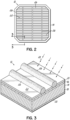
- a cell array 10 of a solar panel includes a plurality of solar cells 12.
- the cell array 10 may be a package of components including a front sheet, a rear sheet, and encapsulant layers (e.g., ethylene vinyl acetate).
- a silicon substrate lies between the front sheet and the rear sheet between the encapsulant layers. Interconnections are needed to electrically connect the cells 12 within the array 10 together.
- These components maybe enclosed within a frame (not shown).
- the number of cells 12 within the array 10 may vary from that shown.
- solar panels may include sixty cells or more. Other common cell counts are 72 and 90. But, embodiments of the invention are not limited to any number of solar cells 12 in the cell array 10.
- one or more of the cells 12 may include one or more electrical conductors (i.e., electrodes) containing copper.
- the largest proportion of the metal conductors may be copper with the remaining proportion being of other metals and/or metal-containing materials.
- one or more of the solar cells 12 is free of silver.
- the solar cells 12 may be produced in a cost-effective manner as copper-containing conductors replace silver conductors.
- the copper-containing conductors are produced from a copper-containing paste in a metallization process.
- the pastes of the present invention may be substituted into processes that currently utilize silver-containing pastes, such as solar cell/panel manufacturing processes. As will be appreciated, this eliminates the necessity of large capital investments observed with copper electroplating techniques while providing a cost-effective process for producing a solar cell having predominately copper electrodes and in which silver is absent.
- the solar cell 12 includes a semiconductor substrate or wafer 14.
- the wafer 14 is monocrystalline silicon. However, embodiments of the invention are equally applicable to polycrystalline silicon substrates as well as other semiconductor substrates and films.
- the wafer 14 may include an n-type doped silicon region 16 adjacent a p-type doped silicon region 18 to form a p-n junction.
- Other architectures may include a reversal of the p and n doped regions and the incorporation of localized doped regions. The combination of regions 16 and 18 permits separation of electrons from holes when the silicon is struck by photons of light.
- An anti-reflective coating 20 covers the n-type doped silicon region 16 and defines a front surface 22 of the solar cell 12.
- the anti-reflective coating 20 may be silicon nitride (SiN).
- the anti-reflective coating 20 reduces the amount of reflection of the incident light (shown by arrows 24 in Fig. 3 ) from the front surface 22 and thereby increases the portion of incident light 24 that impinges the wafer 14.
- the anti-reflective coating 20 also assists in passivating the surface of the silicon wafer 14, which reduces recombination losses. This improves the electrical efficiency of the solar cell 12.
- the fingers 26 made as described herein have a conductivity that is 2 times to 10 times less conductive than bulk metallic copper.
- the resistivity of the fingers is the reciprocal of their conductivity.
- the backside conductor 30 may be formed of aluminum or another electrical conductor, which has a thickness in the range of 10 ⁇ m to 100 ⁇ m.
- the fingers 26 may be formed from a copper-containing paste and so replace silver-containing pastes in the manufacture of the solar cell 12.
- a copper-containing paste 32 (shown in Fig. 4 ) according to one embodiment of the invention is placed on the front surface 22 of a substrate 40.
- the copper-containing paste 32 may be screen printed on the substrate 40 or dispensed by another method.
- the substrate 40 includes the anti-reflective coating 20 and the wafer 14.
- the backside conductor 30 is made of aluminum, it may already be present (as shown) or may be formed during a process of producing the fingers 26.
- the substrate 40, anti-reflective coating 20, wafer 14, backside conductor 30, and paste 32 are used or deposited to produce the cell 12 shown in Fig. 2 .
- the copper-containing paste 32 defines an elongated body (e.g., a line) having a height, a width, and a length on the substrate 40.
- the elongated body is transformed into a finger during firing of the paste 32, described below.
- the paste 32 includes a plurality of particles 42 contained in an organic vehicle 44.
- the rheological properties of the paste 32 may be adjusted by changing the composition of the organic vehicle 44 and/or the particles 42 to permit the paste 32 to be dispensed via a screen-printing process (e.g., similar to that utilized to screen print a silver-containing paste onto silicon wafers) or by another method.
- the rheological properties of the paste 32 are sufficient to permit the paste 32 to be dispensed while also permitting the paste 32 to maintain a dispensed pattern and not run across the substrate 40; thus allowing the fingers to maintain a high aspect ratio (finger height/finger width)
- the organic vehicle 44 may be a mixture of organic binders together with one or more solvents, dispersants, viscosity modifiers and/or surface tension modifiers.
- binders include polyvinylpyrrolidone (PVP), ethyl cellulose, and monosaccharides, such as fructose.
- solvents include alcohols, ester alcohols, and glycols, such as propylene glycol, ethylene glycol, polyethylene glycol, Texanol TM ester alcohol, as well as ether alcohols and glycols, such as diethylene glycol and triethylene glycols, in addition to water.
- Exemplary viscosity and surface tension modifiers include DISPERBYK ® 111, DISPERBYK ® 180, DISPERBYK ® 190, RHODAFAC ® RE-610, and sodium stearate, to name only a few.
- the volume of the organic vehicle 44 in the paste 32 and the proportion of each type of particle 42 can be tuned to meet a desired rheological (e.g. viscosity) specification.
- the paste 32 may comprise of only a few weight percent organic vehicle 44.
- the paste 32 includes the organic vehicle 44 in a range from 1 wt.% to 15 wt.%.
- the copper-containing paste 32 is a mixture of particles of differing composition. That is, the paste 32 may be a mixture of powders that provide all the particles 42. Each one of the powders may include particles 42 having different composition, particle size, and/or particle shape.
- the copper-containing paste 32 includes a plurality of copper-containing particles 46 that form the largest portion by volume of the particles 42 in the paste 32.
- the copper-containing particles 46 may form the majority volume of the fingers 26. With the make-up of the particles 42, following firing, the fingers 26 are capable of providing electrical conductivity, via metallic copper or copper-containing metal, sufficient to promote efficient solar cell performance.
- the copper-containing particles 46 may be metallic copper and form from 48 vol. % to 88 vol.% of the solids in the paste 32. This may translate into at least 80 wt.% copper metal in the paste 32 before drying.
- the range of copper metal in the paste 32 may be from 62 wt.% to 98 wt.%.
- the copper-containing particles 46 are described with reference to metallic copper, the copper-containing particles 46 are not limited to metallic copper, which may include minor impurities elements.
- the copper-containing particles 46 may be particles of a copper-containing alloy or copper-containing non-metallic (e.g., oxide) particles capable of being reduced to copper or to a copper-containing alloy.
- Copper-containing alloys are those that contain copper as their principal component, for example, bronze (a copper-tin alloy) and brass (a copper-zinc alloy).
- copper-alloys may include copper in combination with other metal elements including nickel, aluminum, and/or lead. Copper-phosphorous alloys are also contemplated.
- the copper-containing particles 46 may be a mixture of two or more of metallic copper, copper-containing alloy, and non-metallic copper-containing material.
- the copper-containing particles 46 are provided in the paste 32 by a powder that is described by a particle size distribution.
- a particle size distribution for one copper powder may include particles in a range of from 10 ⁇ m to 22 ⁇ m in size. That is, the powder contains particles from 10 ⁇ m in size up to 22 ⁇ m in size with an average particle size in the range.
- a narrower particle size distribution of copper-containing particles 46 includes particles ranging from 10 ⁇ m to 20 ⁇ m in size.
- Other exemplary examples include progressively narrower particle size distributions, particle size distributions with particles in the range of 7.5 ⁇ m to 14.7 ⁇ m (these are D 10 and D 90 , respectively), 1.8 ⁇ m to 7.7 ⁇ m (these are D 10 and D 90 , respectively), 1.2 ⁇ m to 3.2 ⁇ m (these are D 10 and D 90 , respectively), or 0.2 ⁇ m to 1.6 ⁇ m (these are D 10 and D 90 , respectively).
- the copper-containing particles 46 may be particles from one powder having a particle size distribution (e.g., one of the exemplary distributions above), or a mixture of multiple different powders such that there are multiple distinct particle size distributions mixed in the paste 32.
- the particle size distribution correlates with the surface area per unit weight of the powder. Thus, as the particle size distribution is shifted to smaller particles, the surface area per gram of the powder increases.
- a powder of coarse copper-containing particles 46 may be mixed with a powder of fine copper-containing particles 46.
- the fine copper-containing powder 46 may fill in the interstices between the larger copper-containing particles 46 in the paste 32. This results in a bimodal particle size distribution of copper-containing particles 46 in the paste 32 and may maximize the volume of copper in the paste 32.
- combinations of any two or more of the particle size distributions identified above may be mixed together to adjust the volume percentage of copper in the paste 32 to be within a desired range.
- the ratio of different sized copper-containing powders by weight may range from 60 wt.% coarse - 40 wt.% fine to 90 wt.% coarse - 10 wt.% fine.
- a coarse copper powder having a particle size distribution with a range in particle size from 10 ⁇ m to 20 ⁇ m may be mixed with a fine copper powder having a particle size distribution with a range of 1.2 ⁇ m to 3.2 ⁇ m at a ratio of 90 wt.% coarse to 10 wt.% fine.
- Other ratios of two or more copper powders are possible, for example, a coarse copper powder having a particle size distribution with a range of particles sizes from 7.5 ⁇ m to 14.7 ⁇ m may be mixed with a fine copper powder having a particle size distribution with a range of particle sizes from 1.2 ⁇ m to 3.2 ⁇ m at a ratio of 70 wt.% coarse to 30 wt.% fine.
- a particle size distribution with a range of particle sizes from 10 ⁇ m to 22 ⁇ m is mixed with three other copper-containing powders having particle size distributions with ranges from 7.5 ⁇ m to 14.7 ⁇ m, from 1.8 ⁇ m to 7.7 ⁇ m, and from 1.2 ⁇ m to 3.2 ⁇ m at a weight ratio of 37 to 21 to 12 to 30, respectively.
- Copper-containing powders according to embodiments of the invention are commercially available from the Bean Town (copper flakes), Chemical Store (item Cu112SP), ACuInternational (items 610 and 603), and Ames Goldsmith (item C1-2000).
- the copper-containing paste 32 in Fig. 4 is a schematic representation. While the particles 42 within the paste 32 are shown as a spherical morphology, embodiments of the invention are not limited to any single one of the particles being spherical. Other particle morphologies are possible, namely flakes, acicular, faceted, dendritic, spongey, rounded, porous, oblong, wire, and decorated, to name only a few.
- the paste 32 includes other particles 42 differing in at least composition from the copper-containing particles 46.
- the other particles 42 in the paste 32 include nanoparticles 50.
- the nanoparticles 50 are each a discrete object where all three dimensions are equal to or less than 100 nm.
- the nanoparticles 50 may form agglomerates or aggregates in which case the agglomerate or aggregate may measure up to 1 ⁇ m in each orthogonal direction.
- the nanoparticles 50 are metals, metal oxides, and/or metal hydroxides of one or more of nickel (Ni), copper (Cu), lead (Pb), cobalt (Co), manganese (Mn), and silver (Ag).
- mixed element nanoparticles may include Cu, Ni, and Pb; Ni, Ni, and Pb; or Mn, Mn, and Pb.
- nanoparticles 50 include nanoparticles of mixed oxides of Cu/Ni/Pb, Cu-Ag/Ni/Pb nanoparticles, mixed oxides of Co/Co/Pb nanoparticles, mixed oxides of Ni-Co/Ni/Pb nanoparticles, mixed oxides of Ni-Ag/Ni/Pb nanoparticles, and mixed oxides of Mn/Mn/Pb nanoparticles.
- each metal in the A/B/C notation e.g.
- Cu/Ni/Pb may be provided by a metal salt such that a Ni/Ni/Pb nanoparticle is synthesized with Ni being provided by two different nickel-containing salts. Those metals may be oxidized during synthesis.
- the nanoparticles 50 may be doped with one or more of phosphorous (P), chloride (Cl), and boron (B), which may be due to the process by which the nanoparticles 50 are synthesized.
- An exemplary process for making the nanoparticles 50 is described below with reference to Figs. 7A and 7B .
- the nanoparticles 50 are included in the paste 32 in an amount sufficient to reduce or eliminate oxidation of metallic copper or copper alloy either in the paste 32 or formed during manufacturing of the solar cell 12, described further below, while also reducing copper diffusion into the wafer 14 during use of the solar cell 12.
- the nanoparticles 50 may also enable etching of the anti-reflective coating 20 and permit an electrical connection of the copper with the wafer 14. Reduction in copper diffusion may be by way of forming a barrier between copper of the fingers 26 and the wafer 14 during manufacturing. Without being bound by any theory, the nanoparticles 50 are believed to participate in the formation of the barrier so that elements of the nanoparticles 50 form an interface between the silicon of the wafer 14 and the copper from the copper-containing particles 46.
- the nanoparticles 50 may be present in an amount up to 17 wt.% in the paste 32. And, as further examples, the nanoparticles 50 may be present in a detectable amount up to 5 wt.%; a detectable amount up to 3 wt.%; from about 0.2 wt.% (or near a lower limit of detection) up to 3 wt.%; or from about 0.2 wt. % up to 5 wt. % in the paste 32. Mixtures of different nanoparticles are also contemplated with the total weight of the mixture falling within the ranges above. For example, a mixture of nanoparticles 50 may be 50 wt.% Ni/Ni/Pb nanoparticles and 50 wt.% Cu/Ni/Pb nanoparticles.
- the copper-containing particles 46 may be surface modified.
- the particles 46 are coated with smaller particles 56 that surround at least portions of each individual copper-containing particle 46.
- the copper-containing particles 46 are, in essence, encrusted with smaller particles 56.
- the particles 56 may cover the entirety of each particle 46. However, the particles 56 may cover only patches of each surface of the particle 46 and so the particles 56 may not be uniformly distributed over the surface of each particle 46. In that arrangement, the uncovered area of the particle 46 is left exposed within the paste 32.
- This configuration of smaller particles covering larger particles results in an increase in the surface area measured from the surface area of the uncoated particles 46 to a surface area of copper particles 46 coated with particles 56.
- the surface area may be increased by up to 20%.
- uncoated copper particles having a surface area of 0.6 m 2 /g may be modified to have a surface area of at least 0.83 m 2 /g.
- the copper-containing particles 46 may be modified to have a surface area in the range of 0.83 m 2 /g to 1.61 m 2 /g.
- the surface area increase is 1.5%.
- a range for the increase in the surface area is from 1.5% to 20%.
- surface modification may also produce an increase in surface area of as high as 3,000% over the surface area of an uncoated particle 46.
- Surface area may be measured via the BET method. Surface area was measured using the Micromeritics ® Gemini VII Series 2390 Surface Area Analyzer.
- the copper containing particles 46 and nanoparticles 50 were degassed in the Micromeritics ® FlowPrep 060 system under a flow of inert gas (nitrogen, N 2 ) at 160°C for 2 hours.
- the degassing procedure causes contaminants such as water to be desorbed from the surface of the powders, and the gas removes it from the sample tube.
- the Gemini unit uses N 2 physisorption to measure the adsorption isotherms of the powders. Multipoint measurements of the isotherms are used to calculate the surface area of the powders using the Brunauer-Emmett-Teller equation. Controlling surface area of the copper-containing particles 46 may control formation of an interface between the finger 26 and the wafer 14.
- the copper-containing particles 46 may be coated with particles 56 according to a process shown in Fig. 9A .
- the particles 56 may be metallic or oxides/hydroxides of various metals.
- the particles 56 may be metallic copper and/or oxides/hydroxides of at least one of copper (Cu), nickel (Ni), and manganese (Mn).
- the particles 56 may be doped with phosphorous (P) due to the process by which they are synthesized, described below.
- the particles 56 may be nucleated and grown on the surfaces of the copper-containing particles 46. As such, the particles 56 may be at least weakly bonded to the surfaces of each of the copper-containing particles 46.
- Embodiments of the invention are not limited to bonding between the particles 56 and any other particle in the paste 32. Being located at the surface, the particles 56 are positioned to shield the copper-containing particles 46 from oxidation or other undesired reaction during manufacturing. Constituents of the particles 56 may form at least a portion of an interface between the finger 26 and the
- the paste 32 includes secondary oxide particles 52. Similar to the particles 56, the secondary oxide particles 52 may also participate in reducing or inhibiting oxidation of the copper in the copper-containing particles 46 while enabling etching of the anti-reflective coating 20. The secondary oxide particles 52 thus permit an electrical connection between copper of the fingers 26 and the wafer 14 during manufacturing, described below. In addition to that or as an alternative, the secondary oxide particles 52 may assist in forming the interface between the copper in the finger 26 and silicon in the wafer 14 to prevent copper diffusion into the silicon during use of the solar cell 12.
- the secondary oxide particles 52 may be reduced to their constituent metal during heating and may then be capable of reducing at least oxide/hydroxide nanoparticles 50 and/or the oxides/hydroxides of the particles 56. Further, the secondary oxide particles 52 alone or in combination with one or both the nanoparticles 50 and the particles 56 may form a liquid sintering aid during manufacturing of the solar cell 12. Liquid phase sintering is a technique used in the sintering of alloys and composites. In a composite containing two materials, the secondary material will have a lower melting point than the first. Consequently, this material will melt at the given processing temperature, while the other remains solid.
- the ratio of the nanoparticles 50 to secondary oxide particles 52 to particles 56 in the paste 32 may at least partially control the etching process between the paste 32 and the anti-reflective coating 20 during firing.
- the secondary oxide particles 52 may be one or more metal oxides having a more negative Gibbs Free Energy of Formation than at least one of the oxides of the nanoparticles 50 and oxides of the particles 56.
- the secondary oxide particles 52 may have a greater negative Gibbs Free Energy of Formation than at least one of copper oxide (Cu 2 O, CuO), lead oxide (PbO, PbO 2 ), or nickel oxide (NiO) at the temperatures to which the wafer 14 and paste 32 are heated during manufacturing.
- the secondary oxide particles 52 are antimony oxide (Sb 2 O 3 ) particles.
- Other secondary oxide particles 52 include, but are not limited to tin oxide (SnO, SnO 2 ), tellurium oxide (TeO), manganese oxide (MnO, MnO 2 ), phosphorous oxides (P 4 O 10 , PO 2 ), bismuth oxide (Bi 2 O 3 ), chromium oxide (Cr 2 O 3 ), and aluminum oxide (Al 2 O 3 ).
- the use of these oxides to reduce other oxides in the paste 32 may depend on the oxidation state of the secondary oxide particles 52, the melting point temperature of the secondary oxide particles 52, the processing temperature and the partial pressure of a reducing environment surrounding the secondary oxide particles 52.
- the secondary oxide particles 52 may include frit particles, such as lead-containing silicate glasses or other metal-containing glasses that contain one or more oxide components that have a more negative Gibbs Free Energy of Formation than at least one of Cu 2 O, CuO, PbO 2 , PbO, and NiO.
- frit particles include borate glasses, such as B 2 O 3 -PbO-ZnO glass, and silicate glasses, such as PbO-SiO 2 -B 2 O 3 -Al 2 O 3 glass.
- the paste 32 may include from 1 wt.% to 15 wt.% of the secondary oxide particles 52.
- the secondary oxide particles 52 may have a surface area in a range of 2 m 2 /g to 2.5 m 2 /g.
- a ratio of secondary oxide particles 52 to the nanoparticles 50 may determine the amount of oxide reduced and/or the amount of sintering aid that develops during heating.
- a ratio of secondary oxide particles 52 to nanoparticles 50 is in a range of 0.50 to 16.96 by weight.
- a ratio of secondary oxide particles 52 to metal-oxide-containing nanoparticles is in a range of 1.50 to 3.51 by weight.
- "consisting essentially of” means that no other elements or particles are intentionally added to the paste. However, impurity content of other elements in oxide or metallic form from powders or the fabrication process are contemplated.
- the substrate 40 and paste 32 are exposed to temperatures from 20 °C to 400 °C or, more specifically, from 20 °C to 200 °C to dry. During drying at least some of the organic vehicle 44 is removed from the paste 32. This is shown schematically in Fig. 5 by arrows 54.
- the particles 42 of the paste 32 are fired in a metallization process to produce the fingers 26 and/or the backside conductor 30.
- manufacturing of the solar cell 12, including drying and firing is completed in air. That is, the atmosphere during drying and firing is not controlled or modified by addition of inert or reducing gases.
- the particles 42 are exposed to temperatures from 600°C to 930°C in air for from 0.8 s to 10 s depending on the temperature profile of the furnace, belt speed and the composition of the paste 32.
- at least one of the organic binders remaining from the organic vehicle 44 decomposes and forms a reducing environment localized around the particles 42. It is believed that this environment reduces the secondary oxide particles 52.
- the composition of the organic vehicle 44 is believed to reduce antimony oxide (Sb 2 O 3 ) to metallic antimony (Sb).
- the organic vehicle 44 may also reduce lead oxide to lead (Pb).
- the metal from the secondary oxide particle 52 reduces at least some of the nanoparticles 50 and/or the particles 56 on the copper-containing particles 46.
- the metallic Sb generated reduces oxides of the nanoparticles 50 and of the particles 56.
- the metallic Sb may generate Pb by PbO reduction, and Pb may assist in the reduction of copper oxide.
- a cascade-type reduction reaction may be precipitated by decomposition of the organic vehicle 44. In that cascade of reduction, one oxide is reduced to metal. That metal in turn reduces another oxide in the mixture of particles 42.
- the cascade reduction reaction may reduce all oxides in the paste 32 to their constituent metals. This may include any copper oxide present in the paste 32. In that case, a paste containing a large portion of metal oxides, contains a composite of different metals.
- reducing the nanoparticles 50 and the secondary oxide particles 52 may form a liquid sintering aid and may reduce and/or coat the copper-containing particles 46.
- the metal from the nanoparticles 50 and the secondary oxide particles 52 may react with the anti-reflective coating 20. This combination of particles is thought to produce an etchant.
- the particles 42 sinter to form the finger 26 having a width, Wi, and a height, H 1 .
- these dimensions are less than a corresponding width, W 2 , and height, H 2 , of the paste 32 (see Fig. 4 ) following dispensing, shown, for example in Fig. 4 .
- the width W 2 of the paste 32 shrinks to the width, Wi, of the finger 26.
- the height H 2 of the paste 32 is reduced from firing/sintering to H 1 . The reduction in height is at least partly due to reaction/etching of the anti-reflective coating 20, as is described further below.
- the dimensions, e.g., H 1 and W 1 are controlled by factors including, for example, if screen printed, (i) printer setting (e.g., squeegee pressure and speed), (ii) paste rheology and composition, (iii) screen parameters (e.g., opening size), and (iv) firing conditions.
- printer setting e.g., squeegee pressure and speed
- paste rheology and composition e.g., paste rheology and composition
- screen parameters e.g., opening size
- firing conditions e.g., if screen printed, (i) printer setting (e.g., squeegee pressure and speed), (ii) paste rheology and composition, (iii) screen parameters (e.g., opening size), and (iv) firing conditions.
- the finger 26 is metallic as some or all the oxide particles are reduced during firing of the paste 32.
- the finger 26 may be free of internal oxides, excepting that the outer, air exposed surface of the finger 26 may form a native oxide (e.g., CuO and/or Cu 2 O, Sb 2 O 3 , etc.) when exposed to air.
- a native oxide e.g., CuO and/or Cu 2 O, Sb 2 O 3 , etc.
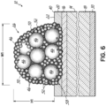
- reaction products may include metal silicides and/or metal nitrides. These reaction products may form an interface 58 (generally indicated in Fig. 6 ) between the copper or copper-containing grains of the finger 26 and the wafer 14 and may include a silicide.
- a composite of metal from the oxide particles 50, 52, and 56 and copper-containing particles 46 that ultimately form the finger 26 come into electrical communication with the n-type region 16 of the wafer 14.
- the interface 58 may prevent copper from diffusing into the silicon of the wafer 14 during fabrication and use of the solar cell 12.
- the interface 58 may form a boundary between the copper or copper-containing grains and the silicon of the wafer.
- the composition of the grain boundaries at the interface 58 may include lead, nickel, copper, cobalt, manganese, antimony, tellurium, and bismuth and/or another metal found in the nanoparticles 50 or the secondary oxide particles 52.
- the backside conductor 30 (e.g., aluminum) is co-fired with the paste 32 in air.
- both the fingers 26 and the backside conductor 30 may be fired simultaneously or separately. It is noted that as the targeted width, Wi, of the finger 26 is reduced, the surface area of the copper-containing particles may be reduced.
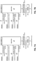
- the paste 32 includes numerous particles 42. Each of these particles may be synthesized prior to their introduction into the organic vehicle 44. As an example, the nanoparticles 50 may be synthesized from various metal salts.
- Figs. 7A and 7B illustrate exemplary flow charts for synthesis of the nanoparticles 50 that may be included in the paste 32.
- Cu/Ni/Pb nanoparticles 50 are synthesized.
- a first aqueous stream 62 of copper nitrate and ammonium hydroxide are added and stirred.
- the ammonium hydroxide causes copper hydroxide and a metal ammonia complex to precipitate.
- a second stream 64 of an aqueous dispersion of sodium borohydride is added to the reactor 60 at a predetermined rate and the solution stirred. The reaction produces copper oxide/hydroxide nanoparticles 50.
- additional streams are added to the reactor 60 containing the copper oxide/hydroxide nanoparticles.
- a third stream 66 of aqueous nickel chloride and aqueous sodium borohydride is added to the reactor 60 and stirred. This coats the copper oxide/hydroxide nanoparticles with a layer of nickel oxide.
- a third layer of lead oxide/hydroxide is coated over the layer of nickel oxide by addition of a fourth stream 68 of aqueous lead nitrate to the reactor 60. This produces a lead oxide/hydroxide coating over the nickel oxide.
- B 2 H 6 is assumed to completely react with H 2 O and all the Cu reduces to Cu 2 O with the addition of NiCl 2 .
- Cu has a multi-valence nature, so can react with Cu 2+ ions.
- Cu + can react with Cl - ions.
- the CuCl can form Cu 2 O. 2CuCl (s) + H 2 O (1) - 2HCl (aq) + Cu 2 O (s)
- NiCl 2 reacts with NaBH 4 to coat the Cu 2 O particles with Ni. 2NiCl 2 (aq) + 4NaBH 4 (aq) - 2Ni (s) + 4NaCl (aq) + 2B(OH) 3 (aq) + H 2 (g) + B 2 H 6 (g)
- Both the Ni and Pb shells may oxidize to NiO and PbO. Less than stoichiometric amounts may be used in the reaction. If so, NaBH 4 is assumed to become the limiting factor, and Equation 1 becomes Equation 7, and Equation 5 becomes Equation 8.
- Equation 3 For non-stoichiometric amounts, Equation 3 becomes Equation 10.
- the nanoparticles 50 are separated from the supernatant by centrifugation. And, at 72, the solid residue, which are the Cu/Ni/Pb nanoparticles, is dried. The nanoparticles 50 may be crushed to break apart agglomerates and then sieved and are ready for use in the paste 32.
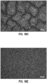
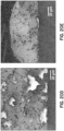
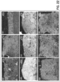
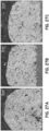
- Fig. 8 depicts transmission electron microscope images of three different Cu/Ni/Pb nanoparticles produced in accordance with the procedure illustrated in Fig. 7A .
- energy-dispersive x-ray maps for Cu are shown in (b), (h), and (n); for oxygen are shown in (e), (i), and (p); for Ni are shown in (d), (j), and (p); for Cl are shown in (e), (k), and (q); and for Pb are shown in (f), (1), and (r).
- the element maps generally indicate the presence and uniform distribution of Cu, O and Ni in the nanoparticle 50. Pb and Cl appear to have a more irregular distribution.
- the nanoparticles 50 produced are Ni/Ni/Pb nanoparticles. That is, the core of the nanoparticle is nickel oxide with a nickel oxide coating and then having a coating of lead oxide. Growing the nickel oxide in two stages generates a larger particle size. In that regard, a first stream 74 of nickel nitrate and ammonium hydroxide are added to the reactor 60. Subsequently, the second stream 64, then third stream 66, and the fourth stream 68 are added to the reactor 60 in a manner similar to that described with reference to Fig. 7A . Following centrifugation 70 and drying 72, Ni/Ni/Pb nanoparticles 50 are ready for addition to the paste 32.
- the copper-containing particles 46 are surface modified with metal oxides prior to mixing the paste 32.
- the copper-containing particles 46 are placed in a reactor 76.
- the copper-containing particles 46 may be pretreated with oleic acid or the particles 46 may be untreated prior to placement in the reactor 76.
- Metal salts e.g., nickel nitrate
- ethylene glycol-water solution containing polyvinylpyrrolidone are dissolved in an ethylene glycol-water solution containing polyvinylpyrrolidone.
- the solution of dissolved metal salt and ethylene glycol is injected into the reactor 76 as a first stream 80 and is mixed with an aqueous dispersion of a reducing agent, such as sodium hypophosphite (NaPO 2 H 2 ), as a second stream 82.
- a reducing agent such as sodium hypophosphite (NaPO 2 H 2 )
- This solution is continuously stirred and heated in the reactor 76 for a prescribed time.
- the metal ions are reduced at the elevated temperatures, and the resulting reaction creates a solution of the copper-containing powders coated with metals or metal oxides/hydroxide.
- the copper-containing particles 46 are coated with nickel oxide and/or nickel hydroxide.
- Particles 56 may coat or decorate the particles 46.
- nickel oxide/hydroxide may include phosphorous and may depend on the concentration of the reducing agent added to the reactor 76.
- the coated particles 46 are separated from the solution at 84 (e.g., via a centrifuge) and then dried at 86.
- the coating on the copper-containing particles 46 may include cobalt (Co) and/or manganese (Mn), among others.
- the surface of the copper-containing particles 46 can be encrusted with particles 56 by adding the copper containing particles 46 to the reactor 76.
- the amount of coating 56 may be controlled by the time that the mixture remains above a specific temperature. In general, as the time and temperature are increased, the surface area of the particle encrusted copper-containing particles 46 increases. By way of example, the total surface area of the copper-containing particles 46 having the particulate coated surface increases.
- the increase in surface area of the particle covered copper-containing particles 46 is at least 10% and may be as high as 3,000% over uncovered particles 46.
- the organic vehicle 44 includes polyvinylpyrrolidone, which is dissolved in the solvent (e.g., polyethylene glycol) and added to a vacuum mixer 92 at 90.
- the solvent e.g., polyethylene glycol
- Nanoparticles, such as the Cu/Ni/Pb nanoparticles 50 from Fig. 9A are also placed in the vacuum mixer 92 at 94.
- the nanoparticles 50 and the organic vehicle 44 are mixed under vacuum for a prescribed time.
- the secondary oxide particles 52 are placed in the vacuum mixer 92.
- the mixture is mixed for a prescribed time under vacuum.
- the mixture is then milled. This may include using a three-roll mill, ball mill or other particle dispersing equipment. The milling process helps to break up particle agglomerates and facilitates homogenization and deaeration of the mixture.
- the mixture is aged at elevated temperatures (e.g., 100 °C) for a prescribed length of time to improve wetting of the organic vehicle 44 on the particles 42.
- the mixture may be subsequently subjected to another round of roll milling at 106 and additional organic vehicle 44 (not shown) may be added to achieve a predetermined viscosity before the paste 32 is ready for use.
- powders may be doped with phosphorous (P) or another element.
- P phosphorous
- (?)P such as "Cu/Ni(?)P”
- Cu/Ni(?)P copper-containing particle with nickel on its surface may be doped with phosphorous.
- the copper or nickel materials in metallic, oxide, or hydroxide form is thought to be doped with P.
- Embodiments of the invention are not limited to those being doped with P or with any other element.
- Example 1 381.24 g (6.0 mols) of copper powder (Example 1 was carried out separately with each of the following copper powders 1.) 10 ⁇ m to 22 ⁇ m, 2.) 7.5 ⁇ m to 14.7 ⁇ m, 3.) 1.8 ⁇ m to 7.7 ⁇ m, and 4.) 1.2 ⁇ m to 3.2 ⁇ m) was gradually added to the mixture. The mixture was continually mixed between the additions to prevent the formation of lumps. The mixture was stirred for 30 minutes with the paddle mixer. 216.24 g (2.0 mols) of sodium hypophosphite monohydrate and 150 mL of distilled water were added to the mixture. The mixture was stirred for 30 minutes with the paddle mixer.
- the mixture was allowed to cool and was transferred to the centrifuge containers.
- the material was centrifuged at 3000 rpm for 3 minutes.
- the supernatant was disposed of into a waste bottle. More of the mixture was added to the centrifuge containers (or distilled water if the mixture beaker has been emptied). Stir and shake the bottle thoroughly. Centrifuging and decanting was repeated until the supernatant was clear and colorless.
- the solid granules were placed on a drying dish and allowed to dry overnight.
- the dried copper-containing particles coated with nickel oxide/hydroxide were crushed with a muller and sieved through a 325 mesh sieve.
- Nickel oxide will deposit on the surface of the copper. Equation 1.
- Nickel nitrate is the rate limiting reagent.
- Synthesis of copper particles with a cobalt-containing particulate coated surface is illustrated by the following example.
- the metal used in the coating can be changed by replacing the metal salt in Example 1 with cobalt nitrate hexahydrate.
- 4.50 g of polyvinylpyrrolidone (PVP) 40,000 is dissolved in 300 mL of ethylene glycol in a 2000 mL flask. The mixture was stirred with a paddle mixer. The mixture was prepared the day before use. 145.52 g (0.5 mols) of cobalt nitrate hexahydrate was added to the PVP/ethylene glycol mixture and mixed until dissolved.
- PVP polyvinylpyrrolidone
- Example 2 381.24 g (6.0 mols) of copper powder (Example 2 was carried out separately using copper powders with a 10 ⁇ m to 22 ⁇ m and a 1.2 ⁇ m to 3.2 ⁇ m size distribution) was gradually added to the mixture. The mixture was continually mixed between the additions to prevent the formation of lumps. The mixture was stirred for 30 minutes with the paddle mixer. 216.24 g (2.0 mols) of sodium hypophosphite monohydrate and 150 mL of distilled water were added to the mixture. The mixture was stirred for 30 minutes with the paddle mixer.
- An aluminum foil lid is placed around the top of the beaker with a hole for the paddle mixer.
- the hot plate temperature was increased to 350 °C, and the mixture was heated for 40 minutes with continual stirring by the paddle mixer.
- the hot plate set at 350 °C, the mixture was permitted to reach the desired temperature of 90 °C. After 40 minutes the hot plate is switched off. The mixture was allowed to cool.
- the mixture was transferred to the centrifuge containers and centrifuged at 3000 rpm for 3 minutes.
- the supernatant was disposed of into a waste bottle. Centrifuging and decanting was repeated until the supernatant was clear and colorless.
- the solid granules were emptied into a drying dish and dried overnight. The dried particle encrusted copper powder was crushed with a muller and sieved through a 325 mesh sieve.
- Synthesis of copper particles with a manganese-containing particulate coated surface is illustrated by the following example.
- the metal used in the coating can be changed by replacing the metal salt in Example 1 with manganese nitrate tetrahydrate.
- 4.50 g of polyvinylpyrrolidone (PVP) 40,000 was dissolved in 300 mL of ethylene glycol in a 2000 mL flask. The mixture was stirred with a paddle mixer. The mixture was prepared the day before use.
- 125.51 g (0.5 mols) of manganese nitrate tetrahydrate was added to the PVP/ethylene glycol mixture and mixed until dissolved.
- Example 3 381.24 g (6.0 mols) of copper powder (Example 3 was carried out separately with each of a 10 ⁇ m to 22 ⁇ m copper powder and a 1.2 ⁇ m to 3.2 ⁇ m copper powder) was gradually added to the mixture. The mixture was continually mixed between the additions to prevent the formation of lumps. The mixture was stirred for 30 minutes with the paddle mixer. 216.24 g (2.0 mols) of sodium hypophosphite monohydrate and 150 mL of distilled water were added to the mixture. The mixture was stirred for 30 minutes with the paddle mixer.
- An aluminum foil lid was placed around the top of the beaker with a hole for the paddle mixer. With the beaker sitting on the hot plate, the hot plate temperature was increased to 350 °C and the mixture was heated for 40 minutes with continual stirring by the paddle mixer. In one example, with the hot plate set at 350 °C, the mixture was permitted to reach 90 °C. After 40 minutes, the hot plate was switched off, and the mixture was allowed to cool.
- the mixture was transferred to the centrifuge containers and centrifuged at 3000 rpm for 3 minutes.
- the supernatant was disposed of into a waste bottle. Decanting and centrifuging was repeated until the supernatant was clear and colorless.
- the solid granules were emptied into a drying dish and dried overnight.
- the dried powder was crushed with a muller and sieved through a 325 mesh sieve.
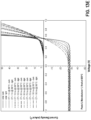
- the surface area of a coated copper powder was controlled by varying the reaction time during synthesis.
- the surface area of the coated powders was directly related to the time at which the reaction mixture remained above the reaction temperature. As the reactants remain above that temperature, the amount of deposited material increases which increases the surface area of the copper powders.
- Fig. 10 in conjunction with Table 1 shows the influence of reaction temperature and time on the surface area of a 1.2 ⁇ m to 3.2 ⁇ m copper powder subject to coating consistent with Example 1.
- the peak temperature in the reactor and the time the reaction mixture remains above 85°C increases the surface area of the coated copper powder.
- the increase is 38% at 90 °C up to a 5-fold increase at 104 °C.
- the surface area of the coated powders is also related to the maximum temperature that the reactants experience during the reaction.
- the reactions using fine (1.2 - 3.2 microns) copper powders with an oleic acid coating are susceptible to temperature overshoot, with the copper powders with an oleic acid coating foaming during the reaction.
- the peak temperature was controlled by the time at which the hot plate was switched off.
- the foam layer collapsed once the reaction reached peak temperature, thus, reducing the thickness of the foam layer.
- This reduction in thickness in addition to a slightly faster stirring rate, resulted in a faster cooling rate for this reaction.
- the heating and cooling curves for the bench scale reactions are within a few degrees (i.e., can be directly superimposed)
- the measured surface area of the coated Cu is within 0.002 m 2 /g.
- a delay ⁇ 1.5 hrs) before the material is centrifuged allows the gases to remain trapped in the foam for a longer period of time. Consequently, the surface area of the coated material was found to increase by 0.126 m 2 /g.
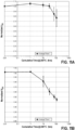
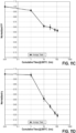
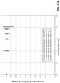
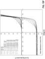
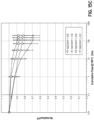
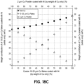
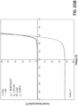
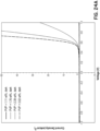
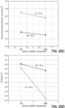
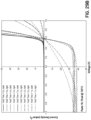
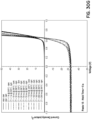
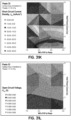
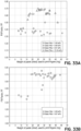
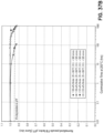
- Figs. 11A-11D Performance of pastes including unmodified copper powders with Ni/Ni/Pb nanoparticles and Sb 2 O 3 particles are shown in Figs. 11A-11D . These figures illustrate an average effect of accelerated aging at 200 °C on (a) the short circuit current density, J sc , ( Fig. 11A ), (b) the open circuit voltage, V oc ( Fig. 11B ) (b) the fill factor, FF, ( Fig. 11C ), and (d) the efficiency, ⁇ ( Fig. 11D ).
- Paste 1 was formulated with Sb 2 O 3 and 100% Ni/Ni/Pb nanoparticles. See Table 12 (below). The copper powders were left uncoated. Results were normalized to their initial values at 0.01 hrs. The error bars are the standard deviation of the results from 5 cells.
- the durability of fired solar cells was determined by monitoring the open circuit voltage (V oc ) of the devices.
- V oc open circuit voltage
- a constant V oc indicates that the copper is not penetrating into the silicon.
- the cells are exposed to an elevated temperature.
- One testing method follows the peer reviewed academic articles for copper electroplated contacts on silicon solar cells. The test thermally stresses the cell at elevated temperatures of 150 °C to 300 °C to evaluate the reliability of the cell over a much shorter period. These temperatures are above the solar cells' maximum operating temperature range of 80 °C to 90 °C.
- One of the drawbacks of this test method is that the testing temperatures are high enough that it is possible to have chemical interactions between the materials, which would never be seen during the normal operation of a solar cell. Diffusion of copper into the junction will lead to a drop in the V oc .
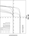
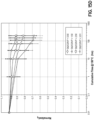
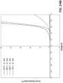
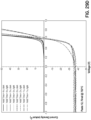
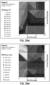
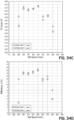
- Pastes 2, 3, and 4 were formulated as shown in Table 2 (below).
- the nanoparticle component of the paste was composed of (i) 100% Cu/Ni/Pb nanoparticles, (ii) 50% Cu/Ni/Pb nanoparticles and 50% Ni/Ni/Pb nanoparticles, and (iii) 100% Ni/Ni/Pb nanoparticles, respectively.
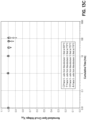
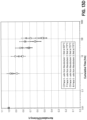
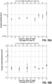
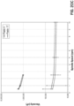
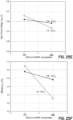
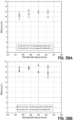
- Fig. 12A illustrates the effect of the nanoparticle composition on the PV performance (i.e., open circuit voltage, V oc ) after the cells were thermally stressed at 200 °C for up to 110 hrs for cells made from each of pastes 2, 3, and 4.
- the error bars in Fig. 12A are the standard deviation for between 4 to 6 cells measured for each paste. Results were normalized to their initial values at 0.01 hrs.
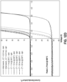
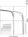
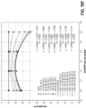
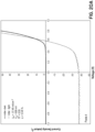
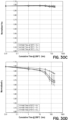
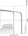
- Figs. 12B , 12C , 12D , and 12E illustrate the effect of accelerated aging on PV performance with Figs. 12B and 12D being 100% Cu/Ni/Pb nanoparticles, Fig. 12C being 50% Cu/Ni/Pb nanoparticles and 50% Ni/Ni/Pb nanoparticles, and Fig. 12E being 100% Ni/Ni/Pb nanoparticles.
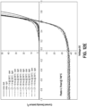
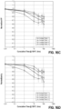
- Figs. 12F, 12G , 12H, and 12I illustrates an average effect of accelerated aging at 200 °C on the (a) short circuit current density, J sc , ( Fig. 12F ), (b) open circuit voltage, V oc , ( Fig. 12G ), (c) fill factor, FF, ( Fig. 12H ), and (d) efficiency, ⁇ ( Fig. 12I ). Results were normalized to their initial values at 0.01 hrs. The error bars are the standard deviation of 4 to 6 cells measured for each paste.
- This example demonstrates an effect of the particulate coating of a copper containing powder on the PV performance of crystalline silicon cells from three different manufacturers.
- the copper powders used a coating consistent with Example 1.
- the cells prepared were thermally stressed at 200 °C for up to 110 hrs.
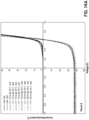
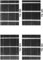
- Performance of paste 5 of Table 3 is shown in Figs. 13A-13H .
- FIGs. 14A , 14B , and 14C show the PV performance of monocrystalline silicon solar cells where the fingers were printed with the following pastes (a) Paste 6, (b) Paste 7, and (c) Paste 8 of Table 4 (below).
- the cells were thermally stressed at 150 °C for up to 300 hrs.
- the proportion of the nanoparticles and secondary oxide particles in these pastes was increased so that the volume (solids only) of copper in the paste ranged from 85.50 vol.% to 79.51 vol.% Cu.
- the proportion of nanoparticles and secondary oxide particles in the paste increased, the thickness of the glassy interface between the finger and the wafer increases.
- the PV performance of the cells during the accelerated aging tests is maintained by maintaining the solids only portion of the paste to be greater than 80 vol.%.
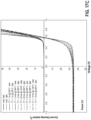
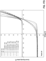
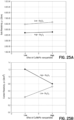
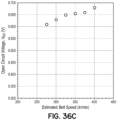
- This example shows the effect of the proportion of secondary oxide particles in the paste on the performance of the cells during accelerated aging tests at 150 °C for up to 200 hrs.
- the weight ratio of the secondary oxide particles to nanoparticles in the pastes were varied by changing the proportion of secondary oxide particles in the paste used to print fingers.
- the total surface area contribution of the coated copper-containing powder used in the pastes was fixed at 0.74 m 2 of coating per gram of paste.
- Table 5 shows the compositions of the pastes used to print the fingers. All the cells used the same bus bar paste formulation.
- a nickel coating on the copper-containing powders was quantified via measurement of the materials surface area.
- the amount of coating in the pastes was varied by changing the surface area of fine copper powders in the paste.
- the amount of coating on the copper powders was (Paste 11) 0.74, (Paste 14) 0.83, (Paste 15) 1.01, and (Paste 16) 1.10 m 2 per gram of paste. All pastes used a secondary oxide particle to nanoparticle ratio of 1.50.
- Table 6 shows the compositions of the pastes used to print the fingers. All the cells used the same bus bar paste formulation.
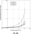
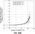
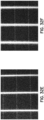
- Figs. 16A, 16B , 16C, 16D , and 16E illustrate the effect of accelerated aging tests at 200 °C on the PV performance normalized J sc , normalized V oc , normalized FF, normalized ⁇ , and normalized resistance across the fingers, respectively, of mono c-Si cells with a PERC localized Al BSF metallized with pastes in Table 6.
- the surface area of the copper containing particle with nickel was greater than 1.0 m 2 per gram of paste, the resistance of the fingers increased significantly; thus, leading to a reduction in FF.
- Using a surface area of 1.01 m 2 per gram of paste on these cells resulted in lowest reduction to the FF ( Fig. 16C ), for the duration of the tests.
- Figs. 17A , 17B , 17C , and 17D illustrates examples of the accelerated aging on the I-V performance of the pastes illustrated in Figs. 16A, 16B , 16C, 16D , and 16E at 200 °C.
- the surface area of the copper-containing particles in the paste was low (Paste 11)
- the diffusion barrier formed by the paste appears to be insufficient, and a noticeable increase in the dark I-V curve was observed; resulting in a lower FF and performance.
- the surface area was high (Paste 16)
- the series resistance of the devices increased significantly, indicating that the barrier was too thick and becoming more resistive under the test conditions.
- This example demonstrates the impact of the surface area of the copper-containing particles used in the paste on the etching functionality of the paste. Both the secondary oxide particles and the nanoparticles are able to etch a silicon nitride (SiN) anti-reflective coating. As the surface area contribution of the copper-containing particle is increased, the capability of the paste to etch through the SiN layer is believed to be reduced. The surface area contribution from the copper-containing particles was varied by varying the ratio of coarse to fine copper-containing powders in the paste. Table 7 lists the effect of changing this ratio on the surface area contribution of the copper-containing powders and its effect on bulk resistivity, contact resistivity, and FF of the devices.
- SiN silicon nitride
- the pastes listed in Table 7 included nanoparticles with a Cu/Ni/Pb composition. It is theorized that during firing, the nanoparticles (Cu/Ni/Pb nanoparticles) and the Sb 2 O 3 secondary oxide particles melt and coat the surface of the copper-containing particles. Consequently, the greater the surface area contribution of the copper-containing particles, the lesser the proportion of nanoparticles and secondary oxides from the secondary oxide particles that reach the cell surface. All samples were fired using the fire brick method. The fire brick method is a technique by which the sample cells were placed on a hot plate set to 300 °C for 3 mins. The sample cells were then immediately transferred to a muffle furnace set to between 750 °C - 800 °C for between 1 s and 3 s.
- the etching process is controlled by the amount of lead (Pb) in the paste, which may be introduced to the paste through the nanoparticles (e.g., Ni/Ni/Pb nanoparticles).
- the molar ratio of Ni:Pb used in the synthesis was 14:1. This amount of Pb was sufficient for a paste containing 0.83 m 2 of copper per gram of paste to etch through the SiN x layer and form a working cell.
- Replacing the coarse copper flakes with the fine (1.2 - 3.2 ⁇ m) copper-containing powders resulted in the paste containing 2.73 m 2 of copper per gram of paste. Consequently, it was believed that the amount of lead in the paste needed to be increased to etch through the SiN x layer.
- the pastes containing 100% of fine (1.2 - 3.2 ⁇ m) copper powders etched through SiN x the ⁇ c of the cell remained high (0.426 ⁇ cm 2 ).
- the main cause of the high ⁇ c was cracking in the finger effecting the measured resistances. Cracking was believed to be due to shrinkage as a result of densification.
- coarse copper flakes were used in the paste.
- the overall surface area of the copper in the paste was maintained at 2.73 m 2 of copper per gram of paste and the quantity of nanoparticles and the secondary oxide (Sb 2 O 3 ) particles was kept constant.
- the amount of binder and solvent in the organic vehicle was adjusted based on the proportion of solids in the paste.
- Figs. 18A , 18B , and 18C shows the effect of the coarse (10 - 20 ⁇ m) to fine (1.2 - 3.2 ⁇ m) copper ratio on the surface area, volume, and weight contribution of the copper-containing with nickel.
- the effect of this ratio on the bulk resistivity ( ⁇ ) and contact resistivity ( ⁇ c ) are shown in Figs. 19A and 19B .
- Figs. 18D and 18E show images of the fired pastes using 100% fine and 100% coarse powders, respectively.
- the pastes containing only fine copper containing powders resulted in large cracks forming, as a result of the densification process occurring during firing. As the amount of coarse copper flakes was increased cracking in the finger was reduced.
- This example shows the impact of the shape of the coarse copper powders on the paste rheology, microstructure and formulation.
- the impact of coarse spherically shaped particles was compared to the coarse flake shaped particles.
- the shape and packing of spherical copper-containing particles allowed the nanoparticles and the secondary oxide particles (Sb 2 O 3 ) particles to melt and flow to the SiN x layer much faster than the interconnecting porous structure of the coarse copper flakes.
- the amount of nanoparticles and secondary oxide particles could be reduced; thus allowing the paste containing spherical particles to have a higher solids loading and a relatively lower viscosity even though the paste contained a higher proportion of fine copper containing particles.
- FIGs. 20A , 20B , and 20C compare I-V performance of those pastes for (a) a 90:10 mixture of (10 - 22 ⁇ m) coarse copper powders and fine (1.2 - 3.6 ⁇ m) copper powders and (b) a 70:30 mixture of (10 - 22 ⁇ m) spherical copper powders and fine (1.2 - 3.6 ⁇ m) copper powders. Cells were measured using a halogen lamp. Comparison of the volume percentage and viscosity of the pastes using coarse (10 - 20 ⁇ m) copper flakes and (10 - 22 ⁇ m) spherical copper powders is shown. In Figs. 20D and 20E , SEM images of fired fingers from (d) coarse powders and (e) large spherical powders are shown, respectively.
- the particles in the paste to pack together as closely as possible with minimum void space.
- the shape and size of the particles, as well as the amount of organic vehicle in the paste will determine how closely the powders will pack.
- Table 9 provides an estimation of the apparent tap density for the different particles used in the paste. The smaller the particle size or the larger the surface area of the particles, the lower the packing density.
- Table 10 shows the ratios of the different powders used in a selection of pastes.
- Figs. 21A, 21B, and 21C shows images of squares printed with the following pastes (a) Paste 18, (b) Paste 19, and (c) Paste 20, respectively. Due to densification and shrinkage, the prints came off the silicon substrate. The squares were placed on a light box, in order to observe the porosity of the fired prints. Squares printed with a higher proportion of fine powders resulted in a denser structure.
- Fig. 22 are SEM cross-sectional images of fingers printed with the pastes specified in Table 10 (above).
- the pastes are (a) Paste 2, (b) Paste 5, (c) Paste 41, (d) Paste 1, (e) Paste 21, (f) Paste 22, (g) Paste 23, (h) Paste 24, and (i) Paste 25. Denser cross sections were obtained for pastes containing a higher proportion of fine powders, as well as a broad particle size range.
- Table 11 shows the full paste composition of Paste 5 shown in Table 10 and Fig. 22(b) .
- Table 12 shows the full paste composition of paste number Paste 1 shown in Table 10 and Fig. 22(d) .
- Paste 1 was formulated so that it would contain the same ratios of secondary oxide particles to nanoparticles to copper containing particles in the paste as was used for Paste 5.
- four different sizes of copper powders (Cu112SP, 610, 603 and C1-2000) were used. It was assumed that the mixing and milling process would allow the Cu112SP, 610 and 603 Cu powders to pack with a packing factor, ⁇ of 0.639 (random ⁇ ).
- Paste 5 Material Ratio by weight of the different Cu powders Weight (g) Volum e (cm 3 ) Packing Volume (cm 3 ) Space (cm 3 ) Wt% (of Paste) Vol% (solids only) 10 - 22 ⁇ m spherical Cu powders (Cu112SP, Chemical Store) 70 116.05 12.95 20.27 7.32 59.88 56.01 7.5 - 14.7 ⁇ m spherical Cu powders (610, ACuInternational) - - - - - - - 1.8 - 7.7 ⁇ m spherical Cu powders (603, ACuInternational) - - - - - - - fine 1.2 3.2 ⁇ m Cu powders (C1-2000, Ames Goldsmith) 30 49.74 5.55 8.69 3.14 25.67 24.01 Sb 2 O 3 - 9.64 1.85 2.90 1.05 4.97 8.02 Ni/Ni/Pb ⁇
- Some of the metals in the paste, specifically in the nanoparticles and in the coating on the surface of the copper-containing powders, are in the form of oxides.
- Introduction of oxides to the electrical contact in the cell will increase the resistivity of the fingers and will reduce the short circuit current density (J sc ), the fill factor (FF), and the overall efficiency ( ⁇ ) of the devices.
- the oxides are advantageous as they are simpler to synthesize and the increased surface area is useful during the etching of the antireflective (SiN) layer. Because of the impact on the overall performance of the solar cell device, these materials must be reduced during the firing.
- Typical techniques to reduce the oxides during the synthesis include the use of hydrogen reductants such as hydrazine, sodium borohydride, etc.
- Forming gases are also a common reductant, but they require specialized furnaces.
- Organic vehicles such as polyvinylpyrrolidone (PVP), decompose at temperatures in excess of 300 °C. That decomposition produces reducing gases capable of reducing metal oxides to metals in the paste. This allows the paste to be fired in air while simultaneously reducing selected oxides present in the paste.
- Exemplary pastes described herein can be used in furnaces commonly used in the PV industry.
- Fig. 23 shows x-ray diffractograms (XRD) of films formulated with Cu/Ni/Pb nanoparticles, lead oxide, and PVP.
- Table 13 lists the composition of the pastes in Fig. 23 .
- the as-deposited films clearly show strong reflections for cuprous oxide (Cu 2 O) and lead oxide (PbO 2 ).
- the films were subjected to a rapid firing process called Intense Pulsed Light (IPL) treatment (also known as photonic sintering). IPL treatment applies multiple pulses of light in rapid succession to a given sample.
- IPL Intense Pulsed Light
- the temperature rise experienced by the films is dependent on the amount of light applied and is a function of the materials' thermal conductivity, specific heat capacity, and density.
- Fig. 23 also shows the film after IPL treatment.
- the intensity of the oxide reflections have diminished and are replaced by intense copper reflections with the films preferentially orientated to the Cu(111) peak location.
- nickel is also present.
- Figs. 24A and 24B illustrate examples of the role of the binder on the etching function of the paste.
- Pastes were formulated with Cu/Ni/Pb nanoparticles and secondary oxide nanoparticles (antimony oxide).
- the amount of organic binder (PVP) in the pastes was adjusted to change the wt.% from 1.01 to 3.02 wt.%.
- the compositions of the pastes can be found in the Table 14 below.
- the pastes were printed on mono crystalline silicon solar cells with a full Al BSF rear contact. The cells were all fired using the fire brick method at 690 °C for 3 s.
- Figs. 24A and 24B show the I-V curves for the cells measured in the dark.
- 24A and 24B also show the impact of firing temperature on the ability of the PVP to etch through the antireflective coating.
- Cells were printed with a paste containing 3.02 wt.% PVP and fired using the fire brick method. The cells were held in the furnace for 3 s. The furnace temperature was varied from 630 - 720 °C. At low temperatures, there was inadequate energy input to adequately etch through the SiN and sinter the copper containing particles. Above high temperatures (720 °C), an increase in dark current is observed, which indicates that the contact appears to have penetrated deeper into the emitter. These results indicate that the firing conditions can be tuned by changing the amount of PVP in the pastes.
- Figs. 31A-31D provide examples of the role of the PVP in the paste.
- the surface area contribution i.e., the amount of nickel particle coating
- the surface area e.g., 1.10, 2.65 and 4.14 m 2 /g
- the effect of the amount of organic binder (PVP) on these different paste compositions was also investigated.
- Table 15 below lists the paste compositions for pastes made with 1.10 m 2 /g of fine copper-containing particles and varying amounts (e.g., 1.5, 2.0, 2.5, and 3.0 wt.%) of PVP.
- Figs. 31A-31O shows that for low surface areas (e.g., 1.01 m 2 /g), low amounts (e.g., 1.5 wt.%) of PVP were enough to reduce the oxides in the paste and etch through the SiN layer.
- the results also indicate that the hold times in zone 2 or the zone 2's setpoint temperature can be reduced further to improve the PV performance of the devices.
- Increasing the amount of PVP in these pastes resulted in a lower performance due to increased series resistance.
- the impact of the secondary oxide particles (e.g., Sb 2 O 3 ) and the nanoparticles (e.g., Cu/Ni/Pb) on the bulk resistivity ( ⁇ ) and contact resistivity ( ⁇ c ) is demonstrated.
- Antimony, Sb is a known n-type dopant for silicon and was introduced as a route to possibly form a n + region below the contact, and hence lower the contact resistivity.
- a commercially available antimony oxide with a particle size range of 1.1 - 1.8 ⁇ m was used.
- Antimony oxide has a low melting point (656 °C) and lies just below nickel oxide, NiO on the Ellingham diagram.
- Figs. 25A, 25B , 25C, 25D , 25E, and 25F illustrate the effect and interactions of varying the levels of the Cu/Ni/Pb nanoparticles and the Sb 2 O 3 particles in the paste on the bulk resistivity ⁇ ( Fig. 25A ), the contact resistivity ⁇ c ( Fig. 25B ), short circuit current density J sc ( Fig. 25C ), fill factor FF ( Fig. 25D ), open circuit voltage V oc ( Fig. 25E ), and efficiency ⁇ ( Fig. 25F ) from a 2 2 factorial design matrix.
- Example 15 Secondary oxide particles acting as a liquid sintering agent
- the secondary oxide particles such as antimony oxide particles, acts as a liquid sintering aid due to their relatively low melting point (for Sb 2 O 3 , melting temperature is 656 °C). A higher proportion of the secondary oxide particles in the paste results in a lower sintering temperature and/or faster sintering process, as well as densification of the contact.
- Table 19 shows the composition of a Paste 38 using a 70:30 blend of coarse to fine copper-containing particles (a similar blend to Paste 5). The amount of secondary oxide particles was increased to about 22 wt.%.
- Figs. 26A and 26B show that although the copper-containing particles appear denser, large voids are present in the microstructure, causing the delamination of the copper contacts from the silicon substrate. Examination of the delaminated contacts using a light box, showed that the contacts still had a significant amount of porosity.
- Paste 38 Material Ratio by weight of the different Cu powders Weight (g) Volume (cm 3 ) Packing Volume (cm 3 ) Space (cm 3 ) Wt% (of Paste) Vol% (solids only) 10 - 22 ⁇ m spherical Cu powders (Cu112SP, Chemical Store) 70 116.05 12.95 20.27 7.32 47.00 38.86 7.5 - 14.7 ⁇ m spherical Cu powders (610, ACuInternational) - - - - - - - 1.8 - 7.7 ⁇ m spherical Cu powders (603, ACuInternational) - - - - - - - fine 1.2 3.2 ⁇ m Cu powders (C1-2000, Ames Goldsmith) 30 49.74 5.55 8.69 3.14 20.14 16.66 Sb 2 O 3 - 55.00 10.58 16.55 5.98 22.27 31.74 Ni/Ni/Pb ⁇ 9.2 Nanop
- the copper-containing particles need to pack together as closely as possible and have a larger volume percentage in the contact.
- packing density studies of the copper-containing particles were carried out using the spherical powders shown in Table 8 (above) of Example 11. Calculations were carried out assuming that the powders had a maximum packing factor of 0.639, and that the smaller spherical powders occupy the free space between the large copper particles. Once this value was calculated, the finest (1.2 - 3.2 ⁇ m) copper powder was added at 30 wt.% of the copper powder in the paste.
- Fig. 22(d) shows an example of a cross section of a contact printed with this blend of particle sizes. Although the contact still shows a high degree of porosity, the increased number of particle-to-particle connections appears to have reduced the size of the pores.
- Figs. 27A, 27B, and 27C show the effect of increasing the amount of secondary oxide particles from (a) 4.98 (Paste 1), to (b) 8.49 (Paste 40) and (c) 12.16 (Paste 39) wt.% on the microstructure.
- the structure shrank, and capillary forces pushed the secondary oxide out of the narrowing pores. Due to this densification and shrinkage the prints came off the silicon substrate. The squares were placed on a light box to observe the porosity in the fired prints.
- Figs. 28A and 28B a photograph of squares printed Paste 39 is shown with Fig. 28A showing the front and Fig. 28B showing the back of the sample. Due to densification and shrinkage, the prints came off the silicon substrate. The squares were placed on a light box, in order to observe the porosity in the fired prints.
- the cells were fired in a semi-automated furnace.
- the system consists of a meter long quartz tube with a volume of approximately 2.4 L.
- the furnace was built with a low temperature zone (zone 1) and a high temperature zone (zone 2) along the length of the quartz tube. Compressed air with a flow rate of 1 L/min was introduced from the start of zone 1.
- the cells were placed on a nichrome mesh stage, which has been automated using a stepper motor andhen software program, for control of the cell's movement speed.
- Zone 1 and zone 2 set point temperatures were 150 °C and 753 °C, respectively.
- the cell was placed on the nichrome mesh and moved into zone 1 at speed, S, where it was held for 180 s. The cell was then moved in to zone 2 at speed, S and held in zone 2 for time, t hold . The stage was then moved back to the start using a speed of 32.4 cm/s. This returned the stage to the start in less than 2 s. The cell was subsequently removed from the stage and rapidly cooled to room temperature by placing it on a metal plate.
- Fig. 29A , 29B , 29C , 29D , and 29E show the current - voltage (I-V) performance of the pastes from Table 21; fired using the method described above.
- the hold times in zone 2 were varied from 1 s to 5 s.
- the paste containing no secondary oxide (Paste 9) was able to etch through the SiN layer using hold times of less than 1 s. This paste, however, etched too deeply, leading to lower PV performance.
- the secondary oxide particles e.g., antimony oxide
- This example shows the effect the copper-containing particles have on the etching and firing conditions of the paste.
- Table 6 shows the compositions of the pastes used in this example. All the pastes used a secondary oxide particles of antimony oxide to nanoparticle (Ni/Ni/Pb) ratio of 1.50. The proportion of nickel nanoparticles in the coating surrounding the copper particles is quantified via the surface area of the coated copper powders.
- the surface area of the fine copper-containing particles in the pastes were varied. This was done by blending different batches of copper powders with surface areas of 1.13, 2.61 and 25.63 m 2 /g to produce pastes containing 0.74 (Paste 11), 0.83 (Paste 14), 1.01 (Paste 15) and 1.10 (Paste 16) m 2 of copper-containing particles per gram of paste.
- Samples were fired using the firing process described in Example 16.
- the cells were fired using zone 2 temperatures of 753 °C, 778 °C, and 803 °C with a stage speed of 1.43 cm/s.
- Table 22 shows the time for which the cells were held in zone 2 to etch through the SiN layer and make a contact to produce FF > 0.6. As shown, the time required increased as the surface area of the copper-containing particles was increased. When a highest zone 2 temperature (i.e., 803 °C) was used, the nickel particles on the copper particles no longer assisted in slowing down the etching process, and actually resulted in the cells being overfired.
- Table 22 Hold Time Zone 2 (s) Zone 2 Temperature (°C) Surface Area contribution from the copper containing particles (m 2 per gram of paste) 753 °C 778 °C 803 °C 0.74 m 2 per gram of paste 3 s 2 s 0 s 0.83 m 2 per gram of paste 4s 3 s 1 s 1.01 m 2 per gram of paste 6 s 3 s 2 s (overfired) 1.10 m 2 per gram of paste 6s 4 s 2 s (overfired)
- This example shows the effect the firing conditions can have on the durability of the cells under accelerated aging conditions.
- the paste was used to metallize mono crystalline silicon solar cells with a full Al BSF rear contact.
- the paste (Paste 15) shown in Table 6 used a total of 1.01 m 2 of copper containing particles with nickel per gram of paste.
- the cells were fired using the procedure described in Example 16 and a stage speed of 1.43 cm/s and zone 2 temperature of 753 °C. The time the cells were held in zone 2 was varied.
- Figs. 30F-30H show exemplary examples of the I-V curves of cells held for 4, 5 and 6 s at 753 °C, respectively.
- the cells were thermally stressed at 200 °C for up to 200 hrs and the PV performance of the devices over the test duration are also shown in Figs. 30A-30E .
- the nanoparticles form an electrical pathway through the glassy interface and also form "spikes" in the surface of the silicon.
- the results show the effect of increasing the firing duration on the lifetime of the cells, with the cells exhibiting improved lifetime after firing for longer firing durations.
- Table 23 shows the compositions of pastes made with no nanoparticles, and with a secondary oxide particle to nanoparticle ratio of 16.75, 8.37, 5.58, 4.19, and 3.35.
- Table 23 Material/Paste ID Paste 42 Paste 43 Paste 44 Paste 45 Paste 46 Paste 47
- Organic Binder PVP 40,000 4.26 g (2.06 wt%) 4.28 g (2.06 wt%) 4.31 g (2.05 wt%) 4.34 g (2.05 wt%) 4.36 g (2.05 wt%) 4.39 g (2.04 wt%)
- Dipropylene Glycol Organic Solvent Tripropylene Glycol 19.85 g (9.37 wt%) 20.09 g (9.42 wt%)
- A/B/C nanoparticles Ni/N
- the amount of paste used to print the fingers directly impacts the maximum secondary oxide particle to nanoparticle ratio that can be used; with fingers using less paste being able to tolerate a relatively smaller ratio, before this cosmetic blemish becomes an issue.
- pastes using a higher ratio require a higher proportion of the overall amount of glass frits (i.e., combined secondary oxides and nanoparticles), as the secondary oxide is a less aggressive etchant than the nanoparticles.
- the finger width (W) dimension decreases (see Fig. 6 )
- the amount of etchants per unit area is reduced. Therefore, this ratio may be reduced further as the finger width is reduced.
- Example 16 shows pastes with a ratio of 0.50.
- Table 21 also shows a paste containing no secondary oxide particles and only nanoparticles
- Table 23 shows a paste containing no nanoparticles and only the secondary oxide particles.
- the finger dimension can be reduced by reducing the number of prints, leading to a reduction in the height of the fingers.
- the height as well as the width of the fingers can also be changed by reducing the dimensions of the pattern, mesh and emulsion thickness used by the screen during the screen-printing process.
- Reducing the height of the fingers reduces the amount of paste on the cell. This reduces the proportion of nanoparticles and secondary oxide particles available per unit area. At a certain point, the amount of these materials is insufficient to etch through the antireflective coating. The etching rate of the combined nanoparticles and secondary oxide particles is lowered by the particles coated on the copper-containing particles. The more particles in the paste, the more nanoparticles and secondary oxide particles are required. However, as the proportion of these materials are increased, the bulk resistivity gradually increases. The quantity of particles in the paste is defined by the surface area of the coated copper-containing particles.
- the amount of power generated by a solar cell is dependent on the number of photons of light reaching the cell. Therefore, the larger the area covered by the electrical conductors, the less photons reach the cell and the lower the power output.
- the surface area for the copper containing particle per gram of paste needed to be reduced.
- a pattern opening size on a screen is reduced. Since, the theoretical maximum particle size should be at least 2.5 times smaller than the mesh opening, the average particle size also needed to be reduced.
- the copper-containing particle has the largest particles in the paste. Consequently, reducing the particle size distribution range of this material naturally leads to an increase in the amount of coating in the paste.
- Figs. 33(a) and 33(b) show the impact of increasing the amount of glass frit and surface area contribution of the copper-containing particles on the amount of paste needed to maintain the fill factor of the device. In Figs.
- the pastes used a secondary oxide to nanoparticle ratio of about 16.75.
- the results show that a reduction in the mass of paste needed to print the fingers can be achieved by reducing the surface area contribution of the copper containing particles from about 0.80 to about 0.57 m 2 per gram of paste.
- the surface area contribution of the copper containing particles was controlled by lowering the surface area of the fine copper powders in the paste from 2.41 m 2 /g to 1.61 m 2 /g.
- the amount of paste used to print the fingers has been controlled by the number prints, that is, 3 prints.
- the reduction in surface area led to the print process being able to use a double print method to achieve devices with a similar performance.
- the screen-printing process was reduced to a single print by reducing the surface area of the fine copper powders down to 1.15 m 2 /g; thus resulting in a total surface area contribution from the copper-containing particle of 0.40 m 2 per gram of paste.
- Full sized poly c-Si cells were printed using pastes with a 0.40 m 2 per gram of paste, and a secondary oxide to nanoparticle ratio of between 16.70 and 16.75.
- the proportion of binder in the pastes was increased from 1.69 to 2.32 wt.%.
- the cells were fired in a TP Solar Model M-225 (Neutrino Series) IR belt furnace. The furnace contained six heated zones and a cooling zone approximately 30% longer that the combined length of the heated sections.
- Zones are built such that the front and rear of the cell were heated simultaneously using IR heat lamps.
- the temperatures for zones 1 through 5 were 620, 460, 440, 450 and 520 °C, respectively.
- Zone 6 was varied from 665 °C to 690 °C.
- the belt speed was varied from 225 - 400 in/min.
- the cells were sectioned into 4 ⁇ 4 cm2 samples in order to measure the PV performance.
- Figs. 34A, 34B , 34C, and 34D show the impact of firing conditions on the PV performance of the full-sized cells sectioned into smaller pieces. For Figs.
- PV performance ((a) short circuit current density, (b) open circuit voltage, (c) fill factor, and (d) efficiency) as a function of the belt speed used to fire the cells in an industrial IR belt furnace.
- the temperature in zones 1 to 5 of the furnace was not changed. Zone 6's temperature was increased from 665 to 690 °C.
- Two versions of the CuBert TM paste, containing 1.69 wt.% binder (Paste 54) and 2.32 wt.% binder (Paste 55) were printed on full-sized poly crystalline silicon cells. The cells were printed with one print. After firing the cells were cut into 4 ⁇ 4 cm 2 sections for measurement. The results shown in Figs. Figs.
- 34A-34D illustrate the average results of between 1/8 to 1/4 of the full-sized cell.
- the compositions of the pastes are shown in Table 25.
- Table 25 Material/Paste ID Paste 54 Paste 55
- Organic Binder PVP 40,000 9.65 g (1.69 wt%) 13.81 g (2.32 wt%)
- Organic Solvent Propylene Glycol 44.97 g (7.88 wt%) 50.90 g (8.54 wt%)
- A/B/C nanoparticles Ni/Ni/Pb NPs 3.09 g (0.54 wt%) 3.18 g (0.53 wt%)
- Cu/D powders Cu/Ni(?)P - fine copper powders (1.2 - 3.2 microns) 138.35 g (24.25 wt%) 142.51 g (23.91 wt%)
- the width and mass of paste used to print the fingers can be decreased further by reducing the size of the screen opening.
- copper-containing particles with a size range of 1.20 to 3.20 ⁇ m were used in the paste.
- Fig. 35 shows the impact of the pastes made using copper-containing particles with a surface area contribution of 0.51 m 2 per gram of paste (Paste 56 - see Table below).
- the pastes used a secondary oxide to nanoparticle ratio of 3.35 and a binder concentration of 3.28 wt.%.
- the mass of paste used to print the fingers on 1/16 th (4 ⁇ 4 cm 2 ) section was lowered to ⁇ 6 mg (about 96 mg for a full-sized cell).
- the pastes were printed on mono crystalline Passivated Emitter Rear Contact (PERC) silicon solar cells and fired using a modified version of the semi-automated furnace described in Example 16.
- PIC Passivated Emitter Rear Contact
- three separate tube furnaces were combined in to one system with a single 122 cm long quartz tube passing through all three furnaces: thus, creating a three-zone furnace. Air flow through the system was controlled by the exhaust gas outlets positioned at either end of the quartz tube.
- the cells were positioned on a nichrome wire stage, which had been automated using a stepper motor andhen software program, for control of the cells speed through the individual zones. The speed of the cell through the different zones was varied to mimic the belt speeds used in the TP Solar IR six zone belt furnace.
- Fig. 35 shows the I-V curve of a cell fired using zone 1, 2 and 3 temperatures of 255, 505 and 990°C, respectively.
- IV Current - Voltage
- a paste Paste 56
- the paste was printed on a mono crystalline silicon PERC cell and was fired using a three zone semi-automated furnace.
- the temperatures in zone's 1, 2 and 3 were 255, 505 and 990°C, respectively.
- the cell was fired with a belt speed of 325 in/min.
- FIGs. 36A , 36C , and 36D shows the impact of firing conditions on the cells' open circuit voltage, V oc for pastes made using a surface area contribution of 0.51, 0.57, and 0.65 m 2 per gram of paste.
- the pastes used a secondary oxide to nanoparticle ratio of 3.35 and a binder concentration of 3.28 wt.%.
- the compositions of the pastes are shown in Table 26 (below). The lower secondary to nanoparticle ratio in combination with lower surface area, result in a significantly reduced V oc at the slower speeds.
- Example 21 Controlling the etching depth and the impact of the binder on durability
- Figs. 37A and 37B show the impact of the proportion of binder in the paste on the durability of the cells under accelerated aging conditions.
- the following apply Effect of accelerated aging tests at 200 °C on the PV performance ((a) open circuit voltage, (b) pseudo fill factor) of poly c-Si cells with a full Al BSF rear contact, metalized with CuBert TM pastes.
- Two versions of the CuBert TM paste, containing 1.69 wt.% binder (Paste 54) and 2.32 wt.% binder (Paste 55) were printed on 6-inch poly c-Si cells.
- the results below show the average results for 4 ⁇ 4 cm 2 sections cut from full sized cells fired in an IR belt furnace using a zone 6 temperature of 665 °C and a belt speed (B.S.) of 300 in/min.
- the charts also show the results of samples fired using a zone 6 temperature of 690 °C and belt speed (B.S). of 325 in/min.
- Poly crystalline cells were printed using pastes containing 1.69 and 2.36 wt.% of binder. The compositions of the paste are provided in Table 25.
- the cells were fired using the six zone TP Solar IR belt furnace described in Example 20.
- the furnace used zone 1, 2, 3, 4 and 5 temperatures of 620, 460, 440, 450, and 520 °C, respectively.
- Zone 6's temperature was changed from 665 to 690 °C.
- the belt speed was varied.
- the full-size cells were cut into smaller 4 ⁇ 4 cm2 pieces, in order to evaluate their PV performance. Accelerated aging tests were carried out by heating the cells at 200 °C under an inert atmosphere for 1000 hrs. The cells were periodically pulled out over the testing period to measure their PV performance.
- the performance was determined by monitoring the open circuit voltage, V oc and pseudo fill factor, pFF measured using a Sinton Instruments Suns-V oc system ( Fig. 37 ).
- the V oc and pFF are sensitive to the diffusion of copper into the junction and are expected to decrease over time if it occurs. The results show that increasing the proportion of binder in the pastes reduces the depth the paste etches into the cells; thereby increasing the durability of the cell.
- the nanoparticles and secondary oxide particles provide the etching functionality of the paste.
- the rate of etching can be varied by changing the ratio of these two materials in the paste. It can also be changed by changing the composition of the nanoparticles.
- the aggressiveness of nanoparticles can be controlled by changing the ratio of the different elements during the synthesis of the nanoparticles, as described above. In this example the molar ratio of nickel (Ni) and lead (Pb) in the Ni/Ni/Pb nanoparticles was decreased from 1.52 to 0.52, during the synthesis.
- Pastes were made using these two nanoparticle compositions and were printed on mono crystalline silicon PERC cells. The cells were fired in the three zone semi-automated firing system described in Example 20.
- Figs. 38A, and 38B show the impact these nanoparticles have on the PV performance.
- the graphs also show the impact of doubling the proportion of nanoparticles and the amount of binder on the PV performance.
- the compositions of the pastes are shown in Table 28.
- Example 23 Impact of the size of the copper containing particles on firing conditions
- 39A, 39B , and 39C show the impact on the lateral resistance of a finger as the temperature in zone 1 was reduced, and the amount of binder in the paste was increased.
- Table 29 shows the composition of the pastes.
- the cells were printed with about 3.5 mg of paste on a 4x4 cm 2 mono crystalline silicon PERC cell.
- Figs. 39A, 39B , and 39C the following apply: impact of firing conditions on the resistance across 22 fingers 3.2 mm in length printed using pastes containing (a) 2.05 (Paste 59), (b) 2.35 (Paste 60), (c) 2.64 (Paste 61) wt.% binder.
- the fingers were printed with approximately 3.5 mg of paste on a 4 ⁇ 4 cm 2 mono crystalline silicon PERC cell.
- Example 24 Increasing the screen life of the pastes for smaller finger dimensions
- the reduction in the size of the particles in the paste can lead to a reduced screen life for the paste, as the increased surface area increases the rate at which the paste dries.
- the screen life can be extended by directly substituting the solvent used in the medium with a solvent with a lower evaporation rate.
- Table 30 shows the physical properties of the solvents that have been tested in the paste.
- Table 31 shows the average dimensions of a high viscosity paste (Paste 53) printed through a 300 mesh screen with a 20 ⁇ m emulsion over mesh (EOM) coating and 100 ⁇ m wide finger opening.
- the cells were fired using a TP Solar six zone IR belt furnace with zone 1, 2, 3, 4, 5 and 6 temperatures of 620, 460, 440, 450, 520 and 840 °C, respectively.
- the average width and height of the fingers for the unfired and fired fingers were measured from cross sectional images using an optical microscope and scanning electron microscope, respectively.
- Fig. 40 shows a cross sectional image of a fired finger. The reduction to the dimensions was due to the densification of the internal structure.
- FIG. 40 The cross-sectional SEM image of a finger (printed with past 53) fired using a TP solar six zone IR belt furnace is shown in Fig. 40 .
- Table 31 Paste ID No. of prints No. of fingers (mg) Average mass of paste used to print fingers on cell 1/16 cell ⁇ 4 ⁇ 4 cm 2 (mg) Screen opening for fingers ( ⁇ m) Average width of unfired fingers ( ⁇ m) Average height of unfired fingers ( ⁇ m) Average width of fired fingers ( ⁇ m) Average height of fired fingers ( ⁇ m) Paste 53 3 18 23 100 115 82 91.8 55.4
- the printed width (see e.g., W 2 in Fig. 4 ) can be reduced further by adjusting the screen. Reducing the finger opening and increasing the mesh count to a higher number leads to smaller openings, thus reducing the amount of paste passing through the screen.
- a screen opening smaller than the target finger width is typically used. In other words, the printed width is usually wider than the corresponding screen opening dimension. Reducing the diameter of the wires in the mesh, as well as the EOM reduces the thickness of the deposit.
- the optical microscope image of the paste (Paste 63) is shown following printing through a 360 mesh screen with 60 ⁇ m wide finger opening (see Fig. 41A ) and a 400 mesh screen with a 35 ⁇ m wide finger opening (see Fig. 41B ).
Landscapes
- Chemical & Material Sciences (AREA)
- Engineering & Computer Science (AREA)
- Organic Chemistry (AREA)
- Chemical Kinetics & Catalysis (AREA)
- Life Sciences & Earth Sciences (AREA)
- Materials Engineering (AREA)
- Physics & Mathematics (AREA)
- General Chemical & Material Sciences (AREA)
- Dispersion Chemistry (AREA)
- Spectroscopy & Molecular Physics (AREA)
- Medicinal Chemistry (AREA)
- Health & Medical Sciences (AREA)
- Polymers & Plastics (AREA)
- Geochemistry & Mineralogy (AREA)
- Wood Science & Technology (AREA)
- Manufacturing & Machinery (AREA)
- Power Engineering (AREA)
- Microelectronics & Electronic Packaging (AREA)
- Computer Hardware Design (AREA)
- General Physics & Mathematics (AREA)
- Condensed Matter Physics & Semiconductors (AREA)
- Ceramic Engineering (AREA)
- Conductive Materials (AREA)
- Sustainable Development (AREA)
- Sustainable Energy (AREA)
- Photovoltaic Devices (AREA)
Claims (16)
- Paste zur Verwendung bei der Metallisierung einer Solarzelle, wobei die Paste Folgendes umfasst:ein organisches Vehikel beinhaltend Polyvinylpyrrolidon, undeine Mischung aus kupferhaltigen Partikeln, metalloxidhaltigen Nanopartikeln und sekundären Oxidpartikeln, die sich von den metalloxidhaltigen Nanopartikeln in dem organischen Vehikel unterscheiden,wobei die sekundären Oxidpartikel Partikel eines Metalloxids beinhalten und ein Metall des Metalloxids in der Lage ist, zumindest einige der metalloxidhaltigen Nanopartikel zu Metall zu reduzieren, wenn die Paste auf eine Temperatur erhitzt wird, bei der sich das organische Vehikel zersetzt,wobei die Nanopartikel jeweils einzelne Partikel sind, bei denen alle drei Dimensionen gleich oder kleiner als 100 nm sind.
- Paste nach Anspruch 1, wobei das organische Vehikel in der Lage ist, das Metalloxid der sekundären Oxidpartikel bei Zersetzung des organischen Vehikels zu reduzieren.
- Paste nach Anspruch 1, wobei die sekundären Oxidpartikel Frittenpartikel beinhalten.
- Paste nach Anspruch 1, wobei die kupferhaltigen Partikel metallische Kupferpartikel und/oder Kupferlegierungspartikel beinhalten.
- Paste nach Anspruch 4, wobei die kupferhaltigen Partikel zumindest ein Metall aus Nickel, Kobalt oder Mangan auf den Oberflächen davon aufweisen.
- Paste nach Anspruch 5, wobei das zumindest eine Metall aus Nickel, Kobalt oder Mangan in der Form eines Metalloxidpartikels ist.
- Paste nach Anspruch 5, wobei die metallischen Kupferpartikel, die Kupferlegierungspartikel und/oder das zumindest eine Metall mit zumindest Phosphor dotiert sind.
- Paste nach Anspruch 5, wobei die Oberflächen der metallischen Kupferpartikel oder die Oberflächen der Kupferlegierungspartikel nicht vollständig durch das zumindest eine Metall bedeckt sind.
- Paste nach Anspruch 1, wobei die metalloxidhaltigen Nanopartikel zumindest ein Oxid von Nickel, Kupfer, Kobalt, Mangan oder Blei beinhalten.
- Paste nach Anspruch 1, wobei die metalloxidhaltigen Nanopartikel Oxide von Nickel und Blei beinhalten.
- Paste nach Anspruch 10, wobei das Metalloxid der sekundären Oxidpartikel Antimonoxid beinhaltet.
- Paste nach Anspruch 1, wobei die metalloxidhaltigen Nanopartikel Oxide von Nickel, Kupfer und Blei beinhalten.
- Paste nach Anspruch 1, wobei das organische Vehikel ein organisches Bindemittel und ein organisches Lösungsmittel ist und wobei das organische Lösungsmittel Propylenglykol ist.
- Paste nach Anspruch 1, wobei das zumindest eine Metall in der Form eines Metallpartikels auf den Oberflächen der kupferhaltigen Partikel ist und die kupferhaltigen Partikel mit metallischen Partikeln einen Oberflächenbereich in der Spanne von 0,7 m2/g bis 5 m2/g aufweisen.
- Verfahren zur Herstellung einer Solarzelle, umfassend:Platzieren einer Paste nach Anspruch 9 auf einer Oberfläche eines Substrats; undErhitzen der Paste auf eine Temperatur, bei der sich das organische Vehikel zersetzt und zumindest einige der Metalloxide zu einem Metall reduziert.
- Solarzelle, die nach dem Verfahren von Anspruch 15 hergestellt ist.
Priority Applications (1)
| Application Number | Priority Date | Filing Date | Title |
|---|---|---|---|
| EP24199943.2A EP4503101A3 (de) | 2019-12-12 | 2020-12-11 | Pasten für solarzellen, solarzellen und verfahren zum herstellen derselben |
Applications Claiming Priority (2)
| Application Number | Priority Date | Filing Date | Title |
|---|---|---|---|
| US201962947316P | 2019-12-12 | 2019-12-12 | |
| PCT/US2020/064514 WO2021119428A2 (en) | 2019-12-12 | 2020-12-11 | Pastes for solar cells, solar cells, and methods of making same |
Related Child Applications (2)
| Application Number | Title | Priority Date | Filing Date |
|---|---|---|---|
| EP24199943.2A Division EP4503101A3 (de) | 2019-12-12 | 2020-12-11 | Pasten für solarzellen, solarzellen und verfahren zum herstellen derselben |
| EP24199943.2A Division-Into EP4503101A3 (de) | 2019-12-12 | 2020-12-11 | Pasten für solarzellen, solarzellen und verfahren zum herstellen derselben |
Publications (4)
| Publication Number | Publication Date |
|---|---|
| EP4073008A2 EP4073008A2 (de) | 2022-10-19 |
| EP4073008C0 EP4073008C0 (de) | 2024-11-20 |
| EP4073008B1 true EP4073008B1 (de) | 2024-11-20 |
| EP4073008B8 EP4073008B8 (de) | 2024-12-25 |
Family
ID=74195097
Family Applications (2)
| Application Number | Title | Priority Date | Filing Date |
|---|---|---|---|
| EP20845247.4A Active EP4073008B8 (de) | 2019-12-12 | 2020-12-11 | Pasten für solarzellen, solarzellen und verfahren zum herstellen derselben |
| EP24199943.2A Pending EP4503101A3 (de) | 2019-12-12 | 2020-12-11 | Pasten für solarzellen, solarzellen und verfahren zum herstellen derselben |
Family Applications After (1)
| Application Number | Title | Priority Date | Filing Date |
|---|---|---|---|
| EP24199943.2A Pending EP4503101A3 (de) | 2019-12-12 | 2020-12-11 | Pasten für solarzellen, solarzellen und verfahren zum herstellen derselben |
Country Status (6)
| Country | Link |
|---|---|
| US (2) | US12243950B2 (de) |
| EP (2) | EP4073008B8 (de) |
| KR (1) | KR102889392B1 (de) |
| CN (3) | CN119403289A (de) |
| ES (1) | ES3002082T3 (de) |
| WO (1) | WO2021119428A2 (de) |
Families Citing this family (2)
| Publication number | Priority date | Publication date | Assignee | Title |
|---|---|---|---|---|
| CN117727491B (zh) * | 2024-01-31 | 2024-06-18 | 江苏富乐华功率半导体研究院有限公司 | 一种用于氮化硅共烧的电子浆料及其制备方法 |
| CN120456662B (zh) * | 2025-07-11 | 2025-09-05 | 鄂尔多斯市隆基光伏科技有限公司 | 太阳能电池及光伏组件 |
Citations (1)
| Publication number | Priority date | Publication date | Assignee | Title |
|---|---|---|---|---|
| CN103700428A (zh) * | 2014-01-13 | 2014-04-02 | 常州时创能源科技有限公司 | 硅太阳能电池电极用导电浆料及其制备方法 |
Family Cites Families (27)
| Publication number | Priority date | Publication date | Assignee | Title |
|---|---|---|---|---|
| US4323483A (en) * | 1979-11-08 | 1982-04-06 | E. I. Du Pont De Nemours And Company | Mixed oxide bonded copper conductor compositions |
| CA1190736A (en) * | 1981-06-03 | 1985-07-23 | Robert J. Moneta | Copper conductor composition for porcelain enamel steel substrates |
| JP4081987B2 (ja) | 2000-05-30 | 2008-04-30 | 株式会社村田製作所 | 金属粉末の製造方法,金属粉末,これを用いた導電性ペーストならびにこれを用いた積層セラミック電子部品 |
| EP2015367A4 (de) | 2006-04-25 | 2011-10-05 | Sharp Kk | Elektroleitfähige paste für eine solarbatterieelektrode |
| MY158807A (en) * | 2009-09-04 | 2016-11-15 | Basf Se | Composition for printing electrodes |
| KR101332429B1 (ko) * | 2009-12-17 | 2013-11-22 | 제일모직주식회사 | 태양전지 전극용 페이스트 및 이를 이용한 태양전지 |
| US9390829B2 (en) * | 2010-01-25 | 2016-07-12 | Hitachi Chemical Company, Ltd. | Paste composition for electrode and photovoltaic cell |
| KR101309809B1 (ko) * | 2010-08-12 | 2013-09-23 | 제일모직주식회사 | 태양전지용 알루미늄 페이스트 및 이를 이용한 태양전지 |
| KR101374359B1 (ko) * | 2010-09-15 | 2014-03-18 | 제일모직주식회사 | 태양전지 전극용 페이스트 및 이를 이용하여 제조되는 태양전지 |
| US8562872B2 (en) * | 2010-09-15 | 2013-10-22 | Cheil Industries, Inc. | Paste for solar cell electrode and solar cell prepared using the same |
| US20110315217A1 (en) * | 2010-10-05 | 2011-12-29 | Applied Materials, Inc. | Cu paste metallization for silicon solar cells |
| CN103443867B (zh) * | 2011-01-18 | 2017-11-14 | 赫劳斯贵金属北美康舍霍肯有限责任公司 | 导电性糊膏组合物以及由其制成的太阳能电极和触点 |
| JP2012212542A (ja) * | 2011-03-31 | 2012-11-01 | Aica Kogyo Co Ltd | ペースト組成物 |
| JP6096468B2 (ja) * | 2011-10-25 | 2017-03-15 | ヘレウス プレシャス メタルズ ノース アメリカ コンショホーケン エルエルシー | 金属ナノ粒子を含有する電気伝導性ペースト組成物 |
| KR101191970B1 (ko) | 2011-12-09 | 2012-10-17 | 한화케미칼 주식회사 | 인 도핑된 니켈 나노 입자 및 이의 제조방법 |
| WO2013090562A2 (en) * | 2011-12-13 | 2013-06-20 | Dow Corning Corporation | Photovoltaic cell and method of forming the same |
| KR102079148B1 (ko) * | 2012-10-19 | 2020-02-19 | 나믹스 가부시끼가이샤 | 도전성 페이스트 |
| US10056505B2 (en) * | 2013-03-15 | 2018-08-21 | Inkron Ltd | Multi shell metal particles and uses thereof |
| TWM512217U (zh) | 2013-06-20 | 2015-11-11 | Plant PV | 太陽能電池 |
| EP2822000B1 (de) * | 2013-07-03 | 2020-10-21 | Heraeus Precious Metals North America Conshohocken LLC | Dicke Kupferdruckpasten für Aluminiumnitridsubstrate |
| JP6293599B2 (ja) * | 2014-07-10 | 2018-03-14 | 京都エレックス株式会社 | 電子デバイスの製法 |
| EP3040320A1 (de) * | 2014-12-31 | 2016-07-06 | Heraeus Precious Metals North America Conshohocken LLC | Glaszusammensetzung für elektrisch leitende pastenzusammensetzungen |
| WO2017091782A1 (en) * | 2015-11-24 | 2017-06-01 | Plant Pv, Inc | Fired multilayer stacks for use in integrated circuits and solar cells |
| KR102553644B1 (ko) * | 2016-02-17 | 2023-07-11 | 나믹스 가부시끼가이샤 | 도전성 페이스트 |
| GB201707670D0 (en) * | 2017-05-12 | 2017-06-28 | Johnson Matthey Plc | Conductiv paste, electrode and solar cell |
| KR102007859B1 (ko) * | 2017-11-06 | 2019-08-06 | 엘에스니꼬동제련 주식회사 | 태양전지 전극용 도전성 페이스트 및 이를 사용하여 제조된 태양전지 |
| KR20190068351A (ko) * | 2017-12-08 | 2019-06-18 | 삼성에스디아이 주식회사 | 태양전지 셀 |
-
2020
- 2020-12-11 EP EP20845247.4A patent/EP4073008B8/de active Active
- 2020-12-11 KR KR1020227023624A patent/KR102889392B1/ko active Active
- 2020-12-11 ES ES20845247T patent/ES3002082T3/es active Active
- 2020-12-11 CN CN202411371058.7A patent/CN119403289A/zh active Pending
- 2020-12-11 CN CN202411368629.1A patent/CN119560212A/zh active Pending
- 2020-12-11 WO PCT/US2020/064514 patent/WO2021119428A2/en not_active Ceased
- 2020-12-11 CN CN202080084323.7A patent/CN115038673B/zh active Active
- 2020-12-11 EP EP24199943.2A patent/EP4503101A3/de active Pending
-
2022
- 2022-06-10 US US17/837,087 patent/US12243950B2/en active Active
-
2025
- 2025-01-31 US US19/042,805 patent/US20250212531A1/en active Pending
Patent Citations (1)
| Publication number | Priority date | Publication date | Assignee | Title |
|---|---|---|---|---|
| CN103700428A (zh) * | 2014-01-13 | 2014-04-02 | 常州时创能源科技有限公司 | 硅太阳能电池电极用导电浆料及其制备方法 |
Non-Patent Citations (1)
| Title |
|---|
| DATABASE WPI Week 201435, 2014 Derwent World Patents Index; AN 2014-J98874 * |
Also Published As
| Publication number | Publication date |
|---|---|
| KR102889392B1 (ko) | 2025-11-21 |
| CN115038673A (zh) | 2022-09-09 |
| KR20220115597A (ko) | 2022-08-17 |
| EP4073008C0 (de) | 2024-11-20 |
| EP4503101A3 (de) | 2025-04-30 |
| EP4503101A2 (de) | 2025-02-05 |
| CN115038673B (zh) | 2024-09-17 |
| WO2021119428A2 (en) | 2021-06-17 |
| WO2021119428A3 (en) | 2021-09-02 |
| CN119403289A (zh) | 2025-02-07 |
| EP4073008B8 (de) | 2024-12-25 |
| US20250212531A1 (en) | 2025-06-26 |
| EP4073008A2 (de) | 2022-10-19 |
| CN119560212A (zh) | 2025-03-04 |
| ES3002082T3 (en) | 2025-03-06 |
| US20220320357A1 (en) | 2022-10-06 |
| US12243950B2 (en) | 2025-03-04 |
Similar Documents
| Publication | Publication Date | Title |
|---|---|---|
| US20250212531A1 (en) | Pastes for solar cells, solar cells, and methods of making same | |
| EP2315638B1 (de) | Metallpulver mit mehreren elementen für siliciumsolarzellen | |
| CN104392771B (zh) | 电极用膏状组合物和光伏电池 | |
| CN104241406B (zh) | 用于硅太阳能电池的核‑壳型镍粒子金属化层 | |
| TW201005755A (en) | Conductive compositions and processes for use in the manufacture of semiconductor devices | |
| TW201120161A (en) | Thick-film conductive compositions with nano-sized zinc additive | |
| EP2689464A2 (de) | Leitfähige pastenzusammensetzung und daraus hergestellte halbleitervorrichtungen | |
| CN1873836A (zh) | 制造半导体器件的方法以及用于该方法的导电组合物 | |
| JP2017199661A (ja) | 導電性ペースト組成物およびそれによって製造される半導体デバイス | |
| TWI745562B (zh) | 導電糊料組成物及用其製成的半導體裝置 | |
| AU2008310924A1 (en) | Conductive nanoparticle inks and pastes and applications using the same | |
| JP2014529644A (ja) | Li2RuO3およびイオン交換されたLi2RuO3を含有する導電性組成物ならびに半導体デバイスの製造におけるそれらの使用 | |
| Jung et al. | Ultrasonic spray pyrolysis for air-stable copper particles and their conductive films | |
| JP2013239695A (ja) | 酸化アンチモンを含有する厚膜組成物および半導体デバイスの製造におけるその使用 | |
| US9951231B2 (en) | Copper-containing conductive pastes and electrodes made therefrom | |
| CN104756198B (zh) | 导电膏组合物及由其制成的半导体器件 | |
| KR20250170134A (ko) | 태양광 셀을 위한 페이스트, 태양광 셀, 및 이를 제조하는 방법 | |
| WO2016029398A1 (en) | Solar cells with copper electrodes | |
| Xiang et al. | Preparation of silver-coated glass frit and its application in silicon solar cells | |
| CN120693991A (zh) | 双面perc太阳能电池单元以及其生产方法 | |
| TW201623638A (zh) | 基於銀奈米粒子之複合太陽能金屬化漿料 |
Legal Events
| Date | Code | Title | Description |
|---|---|---|---|
| STAA | Information on the status of an ep patent application or granted ep patent |
Free format text: STATUS: UNKNOWN |
|
| STAA | Information on the status of an ep patent application or granted ep patent |
Free format text: STATUS: THE INTERNATIONAL PUBLICATION HAS BEEN MADE |
|
| PUAI | Public reference made under article 153(3) epc to a published international application that has entered the european phase |
Free format text: ORIGINAL CODE: 0009012 |
|
| STAA | Information on the status of an ep patent application or granted ep patent |
Free format text: STATUS: REQUEST FOR EXAMINATION WAS MADE |
|
| 17P | Request for examination filed |
Effective date: 20220506 |
|
| AK | Designated contracting states |
Kind code of ref document: A2 Designated state(s): AL AT BE BG CH CY CZ DE DK EE ES FI FR GB GR HR HU IE IS IT LI LT LU LV MC MK MT NL NO PL PT RO RS SE SI SK SM TR |
|
| DAV | Request for validation of the european patent (deleted) | ||
| DAX | Request for extension of the european patent (deleted) | ||
| STAA | Information on the status of an ep patent application or granted ep patent |
Free format text: STATUS: EXAMINATION IS IN PROGRESS |
|
| 17Q | First examination report despatched |
Effective date: 20230627 |
|
| REG | Reference to a national code |
Ref country code: DE Ref legal event code: R079 Free format text: PREVIOUS MAIN CLASS: C03C0008020000 Ipc: C03C0008180000 Ref country code: DE Ref legal event code: R079 Ref document number: 602020041808 Country of ref document: DE Free format text: PREVIOUS MAIN CLASS: C03C0008020000 Ipc: C03C0008180000 |
|
| GRAP | Despatch of communication of intention to grant a patent |
Free format text: ORIGINAL CODE: EPIDOSNIGR1 |
|
| STAA | Information on the status of an ep patent application or granted ep patent |
Free format text: STATUS: GRANT OF PATENT IS INTENDED |
|
| RIC1 | Information provided on ipc code assigned before grant |
Ipc: H01L 21/48 20060101ALI20240423BHEP Ipc: H01L 31/0224 20060101ALI20240423BHEP Ipc: H01B 1/22 20060101ALI20240423BHEP Ipc: C09D 11/52 20140101ALI20240423BHEP Ipc: C09D 11/037 20140101ALI20240423BHEP Ipc: C03C 8/18 20060101AFI20240423BHEP |
|
| INTG | Intention to grant announced |
Effective date: 20240514 |
|
| GRAS | Grant fee paid |
Free format text: ORIGINAL CODE: EPIDOSNIGR3 |
|
| GRAA | (expected) grant |
Free format text: ORIGINAL CODE: 0009210 |
|
| STAA | Information on the status of an ep patent application or granted ep patent |
Free format text: STATUS: THE PATENT HAS BEEN GRANTED |
|
| REG | Reference to a national code |
Ref country code: DE Ref legal event code: R081 Ref document number: 602020041808 Country of ref document: DE Owner name: BERT THIN FILMS, INC., LOUISVILLE, US Free format text: FORMER OWNER: BERT THIN FILMS, LLC, LOUISVILLE, KY, US |
|
| AK | Designated contracting states |
Kind code of ref document: B1 Designated state(s): AL AT BE BG CH CY CZ DE DK EE ES FI FR GB GR HR HU IE IS IT LI LT LU LV MC MK MT NL NO PL PT RO RS SE SI SK SM TR |
|
| REG | Reference to a national code |
Ref country code: GB Ref legal event code: FG4D |
|
| RAP2 | Party data changed (patent owner data changed or rights of a patent transferred) |
Owner name: BERT THIN FILMS, INC. |
|
| REG | Reference to a national code |
Ref country code: CH Ref legal event code: PK Free format text: BERICHTIGUNG B8 Ref country code: CH Ref legal event code: EP |
|
| REG | Reference to a national code |
Ref country code: DE Ref legal event code: R096 Ref document number: 602020041808 Country of ref document: DE |
|
| REG | Reference to a national code |
Ref country code: IE Ref legal event code: FG4D |
|
| U01 | Request for unitary effect filed |
Effective date: 20241205 |
|
| U07 | Unitary effect registered |
Designated state(s): AT BE BG DE DK EE FI FR IT LT LU LV MT NL PT RO SE SI Effective date: 20241213 |
|
| PGFP | Annual fee paid to national office [announced via postgrant information from national office to epo] |
Ref country code: GB Payment date: 20241218 Year of fee payment: 5 |
|
| U20 | Renewal fee for the european patent with unitary effect paid |
Year of fee payment: 5 Effective date: 20241218 |
|
| REG | Reference to a national code |
Ref country code: ES Ref legal event code: FG2A Ref document number: 3002082 Country of ref document: ES Kind code of ref document: T3 Effective date: 20250306 |
|
| PG25 | Lapsed in a contracting state [announced via postgrant information from national office to epo] |
Ref country code: IS Free format text: LAPSE BECAUSE OF FAILURE TO SUBMIT A TRANSLATION OF THE DESCRIPTION OR TO PAY THE FEE WITHIN THE PRESCRIBED TIME-LIMIT Effective date: 20250320 Ref country code: HR Free format text: LAPSE BECAUSE OF FAILURE TO SUBMIT A TRANSLATION OF THE DESCRIPTION OR TO PAY THE FEE WITHIN THE PRESCRIBED TIME-LIMIT Effective date: 20241120 |
|
| PGFP | Annual fee paid to national office [announced via postgrant information from national office to epo] |
Ref country code: ES Payment date: 20250103 Year of fee payment: 5 |
|
| PG25 | Lapsed in a contracting state [announced via postgrant information from national office to epo] |
Ref country code: NO Free format text: LAPSE BECAUSE OF FAILURE TO SUBMIT A TRANSLATION OF THE DESCRIPTION OR TO PAY THE FEE WITHIN THE PRESCRIBED TIME-LIMIT Effective date: 20250220 |
|
| PG25 | Lapsed in a contracting state [announced via postgrant information from national office to epo] |
Ref country code: GR Free format text: LAPSE BECAUSE OF FAILURE TO SUBMIT A TRANSLATION OF THE DESCRIPTION OR TO PAY THE FEE WITHIN THE PRESCRIBED TIME-LIMIT Effective date: 20250221 |
|
| PGFP | Annual fee paid to national office [announced via postgrant information from national office to epo] |
Ref country code: CH Payment date: 20250107 Year of fee payment: 5 |
|
| PG25 | Lapsed in a contracting state [announced via postgrant information from national office to epo] |
Ref country code: PL Free format text: LAPSE BECAUSE OF FAILURE TO SUBMIT A TRANSLATION OF THE DESCRIPTION OR TO PAY THE FEE WITHIN THE PRESCRIBED TIME-LIMIT Effective date: 20241120 |
|
| PG25 | Lapsed in a contracting state [announced via postgrant information from national office to epo] |
Ref country code: RS Free format text: LAPSE BECAUSE OF FAILURE TO SUBMIT A TRANSLATION OF THE DESCRIPTION OR TO PAY THE FEE WITHIN THE PRESCRIBED TIME-LIMIT Effective date: 20250220 |
|
| PGFP | Annual fee paid to national office [announced via postgrant information from national office to epo] |
Ref country code: TR Payment date: 20250122 Year of fee payment: 5 |
|
| PG25 | Lapsed in a contracting state [announced via postgrant information from national office to epo] |
Ref country code: SM Free format text: LAPSE BECAUSE OF FAILURE TO SUBMIT A TRANSLATION OF THE DESCRIPTION OR TO PAY THE FEE WITHIN THE PRESCRIBED TIME-LIMIT Effective date: 20241120 |
|
| PG25 | Lapsed in a contracting state [announced via postgrant information from national office to epo] |
Ref country code: SK Free format text: LAPSE BECAUSE OF FAILURE TO SUBMIT A TRANSLATION OF THE DESCRIPTION OR TO PAY THE FEE WITHIN THE PRESCRIBED TIME-LIMIT Effective date: 20241120 |
|
| PG25 | Lapsed in a contracting state [announced via postgrant information from national office to epo] |
Ref country code: CZ Free format text: LAPSE BECAUSE OF FAILURE TO SUBMIT A TRANSLATION OF THE DESCRIPTION OR TO PAY THE FEE WITHIN THE PRESCRIBED TIME-LIMIT Effective date: 20241120 |
|
| PG25 | Lapsed in a contracting state [announced via postgrant information from national office to epo] |
Ref country code: MC Free format text: LAPSE BECAUSE OF FAILURE TO SUBMIT A TRANSLATION OF THE DESCRIPTION OR TO PAY THE FEE WITHIN THE PRESCRIBED TIME-LIMIT Effective date: 20241120 |
|
| PLBE | No opposition filed within time limit |
Free format text: ORIGINAL CODE: 0009261 |
|
| STAA | Information on the status of an ep patent application or granted ep patent |
Free format text: STATUS: NO OPPOSITION FILED WITHIN TIME LIMIT |
|
| 26N | No opposition filed |
Effective date: 20250821 |
|
| PG25 | Lapsed in a contracting state [announced via postgrant information from national office to epo] |
Ref country code: IE Free format text: LAPSE BECAUSE OF NON-PAYMENT OF DUE FEES Effective date: 20241211 |