EP4071997A1 - Stromumwandlungsvorrichtung - Google Patents
Stromumwandlungsvorrichtung Download PDFInfo
- Publication number
- EP4071997A1 EP4071997A1 EP19955330.6A EP19955330A EP4071997A1 EP 4071997 A1 EP4071997 A1 EP 4071997A1 EP 19955330 A EP19955330 A EP 19955330A EP 4071997 A1 EP4071997 A1 EP 4071997A1
- Authority
- EP
- European Patent Office
- Prior art keywords
- voltage
- value
- evaluation value
- converter cells
- output
- Prior art date
- Legal status (The legal status is an assumption and is not a legal conclusion. Google has not performed a legal analysis and makes no representation as to the accuracy of the status listed.)
- Pending
Links
Images






Classifications
-
- H—ELECTRICITY
- H02—GENERATION; CONVERSION OR DISTRIBUTION OF ELECTRIC POWER
- H02M—APPARATUS FOR CONVERSION BETWEEN AC AND AC, BETWEEN AC AND DC, OR BETWEEN DC AND DC, AND FOR USE WITH MAINS OR SIMILAR POWER SUPPLY SYSTEMS; CONVERSION OF DC OR AC INPUT POWER INTO SURGE OUTPUT POWER; CONTROL OR REGULATION THEREOF
- H02M7/00—Conversion of AC power input into DC power output; Conversion of DC power input into AC power output
- H02M7/42—Conversion of DC power input into AC power output without possibility of reversal
- H02M7/44—Conversion of DC power input into AC power output without possibility of reversal by static converters
- H02M7/48—Conversion of DC power input into AC power output without possibility of reversal by static converters using discharge tubes with control electrode or semiconductor devices with control electrode
- H02M7/53—Conversion of DC power input into AC power output without possibility of reversal by static converters using discharge tubes with control electrode or semiconductor devices with control electrode using devices of a triode or transistor type requiring continuous application of a control signal
- H02M7/537—Conversion of DC power input into AC power output without possibility of reversal by static converters using discharge tubes with control electrode or semiconductor devices with control electrode using devices of a triode or transistor type requiring continuous application of a control signal using semiconductor devices only, e.g. single switched pulse inverters
- H02M7/539—Conversion of DC power input into AC power output without possibility of reversal by static converters using discharge tubes with control electrode or semiconductor devices with control electrode using devices of a triode or transistor type requiring continuous application of a control signal using semiconductor devices only, e.g. single switched pulse inverters with automatic control of output wave form or frequency
- H02M7/5395—Conversion of DC power input into AC power output without possibility of reversal by static converters using discharge tubes with control electrode or semiconductor devices with control electrode using devices of a triode or transistor type requiring continuous application of a control signal using semiconductor devices only, e.g. single switched pulse inverters with automatic control of output wave form or frequency by pulse-width modulation
-
- H—ELECTRICITY
- H02—GENERATION; CONVERSION OR DISTRIBUTION OF ELECTRIC POWER
- H02M—APPARATUS FOR CONVERSION BETWEEN AC AND AC, BETWEEN AC AND DC, OR BETWEEN DC AND DC, AND FOR USE WITH MAINS OR SIMILAR POWER SUPPLY SYSTEMS; CONVERSION OF DC OR AC INPUT POWER INTO SURGE OUTPUT POWER; CONTROL OR REGULATION THEREOF
- H02M1/00—Details of apparatus for conversion
- H02M1/0003—Details of control, feedback or regulation circuits
- H02M1/0006—Arrangements for supplying an adequate voltage to the control circuit of converters
-
- H—ELECTRICITY
- H02—GENERATION; CONVERSION OR DISTRIBUTION OF ELECTRIC POWER
- H02M—APPARATUS FOR CONVERSION BETWEEN AC AND AC, BETWEEN AC AND DC, OR BETWEEN DC AND DC, AND FOR USE WITH MAINS OR SIMILAR POWER SUPPLY SYSTEMS; CONVERSION OF DC OR AC INPUT POWER INTO SURGE OUTPUT POWER; CONTROL OR REGULATION THEREOF
- H02M1/00—Details of apparatus for conversion
- H02M1/0003—Details of control, feedback or regulation circuits
- H02M1/0009—Devices or circuits for detecting current in a converter
-
- H—ELECTRICITY
- H02—GENERATION; CONVERSION OR DISTRIBUTION OF ELECTRIC POWER
- H02M—APPARATUS FOR CONVERSION BETWEEN AC AND AC, BETWEEN AC AND DC, OR BETWEEN DC AND DC, AND FOR USE WITH MAINS OR SIMILAR POWER SUPPLY SYSTEMS; CONVERSION OF DC OR AC INPUT POWER INTO SURGE OUTPUT POWER; CONTROL OR REGULATION THEREOF
- H02M1/00—Details of apparatus for conversion
- H02M1/0067—Converter structures employing plural converter units, other than for parallel operation of the units on a single load
- H02M1/007—Plural converter units in cascade
-
- H—ELECTRICITY
- H02—GENERATION; CONVERSION OR DISTRIBUTION OF ELECTRIC POWER
- H02M—APPARATUS FOR CONVERSION BETWEEN AC AND AC, BETWEEN AC AND DC, OR BETWEEN DC AND DC, AND FOR USE WITH MAINS OR SIMILAR POWER SUPPLY SYSTEMS; CONVERSION OF DC OR AC INPUT POWER INTO SURGE OUTPUT POWER; CONTROL OR REGULATION THEREOF
- H02M7/00—Conversion of AC power input into DC power output; Conversion of DC power input into AC power output
- H02M7/42—Conversion of DC power input into AC power output without possibility of reversal
- H02M7/44—Conversion of DC power input into AC power output without possibility of reversal by static converters
- H02M7/48—Conversion of DC power input into AC power output without possibility of reversal by static converters using discharge tubes with control electrode or semiconductor devices with control electrode
- H02M7/483—Converters with outputs that each can have more than two voltages levels
- H02M7/4833—Capacitor voltage balancing
-
- H—ELECTRICITY
- H02—GENERATION; CONVERSION OR DISTRIBUTION OF ELECTRIC POWER
- H02M—APPARATUS FOR CONVERSION BETWEEN AC AND AC, BETWEEN AC AND DC, OR BETWEEN DC AND DC, AND FOR USE WITH MAINS OR SIMILAR POWER SUPPLY SYSTEMS; CONVERSION OF DC OR AC INPUT POWER INTO SURGE OUTPUT POWER; CONTROL OR REGULATION THEREOF
- H02M7/00—Conversion of AC power input into DC power output; Conversion of DC power input into AC power output
- H02M7/42—Conversion of DC power input into AC power output without possibility of reversal
- H02M7/44—Conversion of DC power input into AC power output without possibility of reversal by static converters
- H02M7/48—Conversion of DC power input into AC power output without possibility of reversal by static converters using discharge tubes with control electrode or semiconductor devices with control electrode
- H02M7/483—Converters with outputs that each can have more than two voltages levels
- H02M7/4835—Converters with outputs that each can have more than two voltages levels comprising two or more cells, each including a switchable capacitor, the capacitors having a nominal charge voltage which corresponds to a given fraction of the input voltage, and the capacitors being selectively connected in series to determine the instantaneous output voltage
-
- H—ELECTRICITY
- H02—GENERATION; CONVERSION OR DISTRIBUTION OF ELECTRIC POWER
- H02M—APPARATUS FOR CONVERSION BETWEEN AC AND AC, BETWEEN AC AND DC, OR BETWEEN DC AND DC, AND FOR USE WITH MAINS OR SIMILAR POWER SUPPLY SYSTEMS; CONVERSION OF DC OR AC INPUT POWER INTO SURGE OUTPUT POWER; CONTROL OR REGULATION THEREOF
- H02M1/00—Details of apparatus for conversion
- H02M1/0043—Converters switched with a phase shift, i.e. interleaved
Definitions
- the present invention relates to a power conversion device.
- Modular multilevel converters including a plurality of unit converters (hereinafter referred to as “converter cells”) connected in cascade are known as large-capacity power conversion devices installed in power systems.
- a converter cell typically includes a plurality of switching elements and a power storage element (typically, capacitor).
- the voltage of a power storage element (capacitor voltage) of each individual converter cell need be maintained in the vicinity of a target value in order to obtain a desired control output. If the capacitor voltage falls out of the target value, the output voltage of the converter cell is not as instructed, so that the control characteristics may be deteriorated, for example, due to occurrence of not-intended circulating current. In a serious case, the capacitor voltage excessively rises or excessively lowers to the level of overvoltage (OV) protection or undervoltage (UV) protection in any converter cell, which may cause the MMC to stop operating.
- OV overvoltage
- UV undervoltage
- the capacitor voltage is usually controlled in multi levels by capacitor voltage control of each individual converter cell (which hereinafter may be referred to as “individual control") as well as by control of converter cells as a whole in the MMC (which hereinafter may be referred to as “all voltage control”) and balance control between certain groups (for example, arms or phases).
- Japanese Patent No. 4999930 (PTL 1) describes control using the mean value (entire mean value) of capacitor voltages of all submodules and the mean value of capacitor voltage in each phase module (phase mean value) in a power conversion device having a plurality of phase modules in which a plurality of submodules (converter cells) are cascaded. Specifically, control of suppressing nonuniformity of stored energy between phases is performed by feedback control of reducing a deviation between a reference value obtained by dividing the entire mean value by the number of phases and a phase mean value.
- the all voltage control and the balance control between groups suppress deficiency and excess of stored energy in the capacitors in the entire power converter and in a certain group.
- a control value of the deficiency and excess is therefore reflected in common to the converter cells as a whole and a plurality of converter cells in a certain group.
- PTL 1 describes the use of the mean value of capacitor voltages of a plurality of converter cells as an evaluation value for stored energy in the converter cells as a whole or a plurality of converter cells in a certain group.
- the controllability may be insufficient in terms of avoiding OV protection or UV protection because information on a converter cell having a large degree of charge or discharge among the converter cells is not reflected in the evaluation value.
- determination of the evaluation value is dependent only on the detection value of the capacitor voltage, the controllability may be deteriorated due to delay in detection of deficiency and excess, because the capacitor voltage is changed as the result of actual deficiency and excess of stored energy.
- the present invention is made in order to solve such a problem, and an object of the present invention is to improve the controllability of the power conversion device by appropriately calculating an evaluation value of the capacitor voltages of a plurality of converter cells for controlling stored energy in units of a plurality of converter cells.
- a power conversion device includes a power converter and a control device to control the power converter.
- the power converter includes at least one arm having multiple converter cells cascaded to each other.
- Each of the converter cells includes a pair of input and output terminals, a plurality of switching elements, a power storage element, and a voltage detector to detect a voltage of the power storage element.
- the power storage element is electrically connected to the input and output terminals through the switching elements.
- the control device includes a voltage macro controller and a voltage evaluation value generator.
- the voltage macro controller controls at least one of: deficiency and excess of stored energy of the power storage elements by all of the converter cells that constitute the power converter; and deficiency and excess of stored energy of the power storage elements by a plurality of converter cells included in each of a plurality of groups obtained by classifying the all of the converter cells in advance.
- the voltage evaluation value generator calculates at least one of: a voltage evaluation value of each power storage element different from a mean value of respective voltage detection values of the power storage elements, for the all of the converter cells; and a voltage evaluation value of each power storage element different from a mean value of respective voltage detection values of the power storage elements, for the plurality of converter cells in each of the groups.
- the voltage macro controller calculates a control value set in common to at least the plurality of converter cells for controlling deficiency and excess of the stored energy, based on the voltage evaluation value from the voltage evaluation value generator.
- the present invention can improve the controllability of the power conversion device by appropriately calculating an evaluation value of the capacitor voltages of a plurality of converter cells for controlling stored energy in units of a plurality of converter cells, using a method different from a simple mean value.
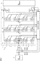
- Fig. 1 is a schematic configuration diagram of a power conversion device 1 according to the present embodiment.
- power conversion device 1 is configured with a modular multilevel converter (MMC) including a plurality of converter cells connected in series to each other.
- MMC modular multilevel converter
- the "converter cell” may be referred to as “submodule”, SM, or "unit converter”.
- Power conversion device 1 performs power conversion between a DC circuit 14 and an AC circuit 12.
- Power conversion device 1 includes a power converter 2 and a control device 3.
- Power converter 2 includes a plurality of leg circuits 4u, 4v, and 4w (denoted as leg circuit 4 when they are collectively referred to or any one of them is referred to) connected in parallel with each other between a positive DC terminal (that is, high potential-side DC terminal) Np and a negative DC terminal (that is, low potential-side DC terminal) Nn.
- Leg circuit 4 is provided for each of a plurality of phases forming alternating current. Leg circuit 4 is connected between AC circuit 12 and DC circuit 14 to perform power conversion between those circuits.
- AC circuit 12 is a three-phase alternating current system, and three leg circuits 4u, 4v, and 4w are provided respectively corresponding to U phase, V phase, and W phase.
- AC input terminals Nu, Nv, and Nw respectively provided for leg circuits 4u, 4v, and 4w are connected to AC circuit 12 through a transformer 13.
- AC circuit 12 is, for example, an AC power system including an AC power source.
- Fig. 1 for simplification of illustration, the connection between AC input terminals Nv, Nw and transformer 13 is not shown.
- DC circuit 14 is, for example, a DC power system including a DC power transmission network or a DC terminal of another power conversion device. In the latter case, two power conversion devices are coupled to form a back to back (BTB) system for connecting AC power systems having different rated frequencies.
- BTB back to back
- AC circuit 12 may be connected through an interconnecting reactor, instead of using transformer 13 in Fig. 1 .
- leg circuits 4u, 4v, and 4w may be provided with respective primary windings, and leg circuits 4u, 4v, and 4w may be connected in terms of alternating current to transformer 13 or the interconnecting reactor through secondary windings magnetically coupled to the primary windings.
- the primary windings may be reactors 8A and 8B described below.
- leg circuits 4 are electrically (that is, in terms of direct current or alternating current) connected to AC circuit 12 through connections provided for leg circuits 4u, 4v, and 4w, such as AC input terminals Nu, Nv, and Nw or the primary windings.
- Leg circuit 4u includes an upper arm 5 from high potential-side DC terminal Np to AC input terminal Nu and a lower arm 6 from low potential-side DC terminal Nn to AC input terminal Nu.
- AC input terminal Nu that is a connection point between upper arm 5 and lower arm 6 is connected to transformer 13.
- High potential-side DC terminal Np and low potential-side DC terminal Nn are connected to DC circuit 14.
- Leg circuits 4v and 4w have a similar configuration, and hereinafter the configuration of leg circuit 4u is explained as a representative example.
- Upper arm 5 includes a plurality of converter cells 7 connected in cascade and a reactor 8A. Converter cells 7 and reactor 8A are connected in series.
- lower arm 6 includes a plurality of converter cells 7 connected in cascade and a reactor 8B. Converter cells 7 and reactor 8B are connected in series.
- Ncell the number of converter cells 7 included in each of upper arm 5 and lower arm 6 is denoted as Ncell. Ncell is ⁇ 2.
- Reactor 8A may be inserted at any position in upper arm 5 of leg circuit 4u, and reactor 8B may be inserted at any position in lower arm 6 of leg circuit 4u.
- a plurality of reactors 8A and a plurality of reactors 8B may be provided.
- the inductances of the reactors may be different from each other.
- Only reactor 8A of upper arm 5 or only reactor 8B of lower arm 6 may be provided.
- the transformer connection may be adjusted to cancel the magnetic flux of DC component current, and leakage reactance of the transformer may act on AC component current, as an alternative to the reactor.
- the provision of reactors 8A and 8B can suppress abrupt increase of accident current at a time of an accident in AC circuit 12 or DC circuit 14.
- Power conversion device 1 further includes an AC voltage detector 10, an AC current detector 16, DC voltage detectors 11A and 11B, and arm current detectors 9A and 9B provided for each leg circuit 4, as detectors for measuring the quantity of electricity (current, voltage, etc.) used in control. Signals detected by these detectors are input to control device 3.
- Fig. 1 the signal lines of signals input from the detectors to control device 3 and the signal lines of signals input and output between control device 3 and converter cells 7 are depicted partially collectively for the sake of ease of illustration, but, in actuality, they are provided individually for each detector and each converter cell 7. Signal lines between each converter cell 7 and control device 3 may be provided separately for transmission and reception.
- the signal lines are formed with, for example, optical fibers.
- AC voltage detector 10 detects U-phase AC voltage Vacu, V-phase AC voltage Vacv, and W-phase AC voltage Vacw of AC circuit 12.
- Vacu, Vacv, and Vacw may be collectively referred to as Vac.
- AC current detector 16 detects U-phase AC current Iacu, V-phase AC current Iacv, and W-phase AC current Iacw of AC circuit 12.
- Iacu, Iacv, and Iacw may be collectively referred to as lac.
- DC voltage detector 11A detects DC voltage Vdcp at high potential-side DC terminal Np connected to DC circuit 14.
- DC voltage detector 11B detects DC voltage Vdcn at low potential-side DC terminal Nn connected to DC circuit 14. The difference between DC voltage Vdcp and DC voltage Vdcn is defined as DC voltage Vdc.
- DC voltage detector 17 detects DC current Idc flowing through high potential-side DC terminal Np or low potential-side DC terminal Nn.
- Arm current detectors 9A and 9B provided in leg circuit 4u for U phase respectively detect upper arm current Ipu flowing through upper arm 5 and lower arm current Inu flowing through lower arm 6.
- Arm current detectors 9A and 9B provided in leg circuit 4v for V phase respectively detect upper arm current Ipv and lower arm current Inv.
- Arm current detectors 9A and 9B provided in leg circuit 4w for W phase respectively detect upper arm current Ipw and lower arm current Inw.
- upper arm currents Ipu, Ipv, and Ipw may be collectively referred to as upper arm currentInventmp
- lower arm currents Inu, Inv, and Inw may be collectively referred to as lower arm current Iarmn
- upper arm currentInventmp and lower arm current Iarmn may be collectively referred to as Iarm.
- Fig. 2(a) and Fig. 2(b) are circuit diagrams showing a configuration example of converter cell 7 that constitutes power converter 2.
- Converter cell 7 shown in Fig. 2(a) has a circuit configuration called half bridge configuration.
- This converter cell 7 includes a series of two switching elements 31p and 31n connected in series, a power storage element 32, a voltage detector 33, and input/output terminals P1 and P2.
- the series of switching elements 31p and 31n and power storage element 32 are connected in parallel.
- Voltage detector 33 detects voltage Vc between both ends of power storage element 32.
- Both terminals of switching element 31n are connected to input/output terminals P1 and P2. With switching operation of switching elements 31p and 31n, converter cell 7 outputs voltage Vc of power storage element 32 or zero voltage between input/output terminals P1 and P2. When switching element 31p is turned ON and switching element 31n is turned OFF, voltage Vc of power storage element 32 is output from converter cell 7. When switching element 31p is turned OFF and switching element 31n is turned ON, converter cell 7 outputs zero voltage.
- Converter cell 7 shown in Fig. 2(b) has a circuit configuration called full bridge configuration.
- This converter cell 7 includes a first series of two switching elements 31p1 and 31n1 connected in series, a second series of two switching elements 31p2 and 31n2 connected in series, a power storage element 32, a voltage detector 33, and input/output terminals P1 and P2.
- the first series, the second series, and power storage element 32 are connected in parallel.
- Voltage detector 33 detects voltage Vc between both ends of power storage element 32.
- converter cell 7 outputs voltage Vc, -Vc of power storage element 32 or zero voltage between input/output terminals P1 and P2.
- switching elements 31p, 31n, 31p1, 31n1, 31p2, and 31n2 are configured, for example, such that a freewheeling diode (FWD) is connected in anti-parallel with a self-turn-off semiconductor switching element such as an insulated gate bipolar transistor (IGBT) or a gate commutated turn-off (GCT) thyristor.
- FWD freewheeling diode
- IGBT insulated gate bipolar transistor
- GCT gate commutated turn-off
- a capacitor such as a film capacitor is mainly used for power storage element 32.
- Power storage element 32 may hereinafter be called capacitor.
- voltage Vc of power storage element 32 may be referred to as capacitor voltage Vc.
- converter cells 7 are connected in cascade.
- input/output terminal P1 is connected to input/output terminal P2 of adjacent converter cell 7 or high potential-side DC terminal Np
- input/output terminal P2 is connected to input/output terminal P1 of adjacent converter cell 7 or AC input terminal Nu.
- converter cell 7 arranged in lower arm 6 input/output terminal P1 is connected to input/output terminal P2 of adjacent converter cell 7 or AC input terminal Nu
- input/output terminal P2 is connected to input/output terminal P1 of adjacent converter cell 7 or low potential-side DC terminal Nn.
- converter cell 7 has the half bridge cell configuration shown in Fig. 2(a) , and a semiconductor switching element is used as a switching element, and a capacitor is used as a power storage element, by way of example.
- converter cell 7 that constitutes power converter 2 may have the full bridge configuration shown in Fig. 2(b) .
- a converter cell having a configuration other than those illustrated in the examples above, for example, a converter cell having a circuit configuration called clamped double cell may be used, and the switching element and the power storage element are also not limited to the examples above.
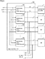
- Fig. 3 is a functional block diagram illustrating an internal configuration of control device 3 shown in Fig. 1 .
- control device 3 includes a switching control unit 501 for controlling ON and OFF of switching elements 31p and 31n of each converter cell 7.
- Switching control unit 501 includes a U-phase basic controller 502U, a U-phase upper arm controller 503UP, a U-phase lower arm controller 503UN, a V-phase basic controller 502V, a V-phase upper arm controller 503VP, a V-phase lower arm controller 503VN, a W-phase basic controller 502W, a W-phase upper arm controller 503WP, and a W-phase lower arm controller 503WN
- U-phase basic controller 502U, V-phase basic controller 502V, and W-phase basic controller 502W may be collectively referred to as basic controller 502.
- U-phase upper arm controller 503UP, U-phase lower arm controller 503UN, V-phase upper arm controller 503VP, V-phase lower arm controller 503VN, W-phase upper arm controller 503WP, and W-phase lower arm controller 503WN may be collectively referred to as arm controller 503.
- Fig. 4 shows a hardware configuration example of the control device.
- Fig. 4 shows an example in which control device 3 is configured with a computer.
- control device 3 includes one or more input converters 70, one or more sample hold (S/H) circuits 71, a multiplexer (MUX) 72, and an A/D converter 73.
- Control device 3 further includes one or more central processing units (CPU) 74, random access memory (RAM) 75, and read only memory (ROM) 76.
- Control device 3 further includes one or more input/output interfaces 77, an auxiliary storage device 78, and a bus 79 connecting the components above to each other.
- Input converter 70 includes an auxiliary transformer (not shown) for each input channel.
- Each auxiliary transformer converts a detection signal from each electrical quantity detector in Fig. 1 into a signal having a voltage level suitable for subsequent signal processing.
- Sample hold circuit 71 is provided for each input converter 70. Sample and hold circuit 71 samples and holds a signal representing the electrical quantity received from the corresponding input converter 70 at a predetermined sampling frequency.
- Multiplexer 72 successively selects the signals held by a plurality of sample hold circuits 71.
- A/D converter 73 converts a signal selected by multiplexer 72 into a digital value.
- a plurality of A/D converters 73 may be provided to perform A/D conversion of detection signals of a plurality of input channels in parallel.
- CPU 74 controls the entire control device 3 and performs computational processing under instructions of a program.
- RAM 75 as a volatile memory
- ROM 76 as a nonvolatile memory are used as a main memory of CPU 74.
- ROM 76 stores a program and setting values for signal processing.
- Auxiliary storage device 78 is a nonvolatile memory having a larger capacity than ROM 76 and stores a program and data such as electrical quantity detection values.
- Input/output interface 77 is an interface circuit for communication between CPU 74 and an external device.
- control device 3 may be configured using circuitry such as a field programmable gate array (FPGA) and an application specific integrated circuit (ASIC). That is, the function of each functional block illustrated in Fig. 3 may be configured based on the computer illustrated in Fig. 4 or may be at least partially configured with circuitry such as an FPGA and an ASIC. At least a part of the function of each functional block may be configured with an analog circuit.
- FPGA field programmable gate array
- ASIC application specific integrated circuit
- Fig. 5 is a block diagram illustrating a configuration example of basic controller 502 shown in Fig. 3 .
- basic controller 502 includes an arm voltage command generator 601.
- Control device 3 further includes a voltage evaluation value generator 700 to generate a voltage evaluation value Vcg to be used in arm voltage command generator 601.
- Arm voltage command generator 601 calculates an arm voltage command value krefp for the upper arm and an arm voltage command value krefn for the lower arm.
- krefp and krefn are collectively referred to as kref.
- Voltage evaluation value generator 700 receives capacitor voltage Vc detected by voltage detector 33 in each converter cell 7. Voltage evaluation value generator 700 generates, from capacitor voltage Vc of each converter cell 7, an all voltage evaluation value Vcgall for evaluating the total sum of stored energy of capacitors 32 of all converter cells 7 in power converter 2 and a group voltage evaluation value Vcgr indicating the total sum of stored energy of capacitors 32 of converter cells 7 in each of predetermined groups.
- group voltage evaluation value Vcgr includes a U-phase voltage evaluation value Vcgu, a V-phase voltage evaluation value Vcgv, and a V-phase voltage evaluation value Vcgv for evaluating the total sum of stored energy of a plurality of (2 ⁇ Necll) converter cells 7 included in each of leg circuits 4u (U phase), 4v (V phase), and 4w (W phase).
- group voltage evaluation value Vcgr may include group voltage evaluation value Vcgr for evaluating the total sum of stored energy of a plurality of (Necll) converter cells 7 for each of upper arm 5 and lower arm 6 for each leg circuit 4.
- all voltage evaluation value Vcgall and group voltage evaluation value Vcgr generated by voltage evaluation value generator 700 are collectively referred to as voltage evaluation value Vcg.
- these voltage evaluation values Vcg are determined as the mean value of capacitor voltages Vc of all of converter cells 7 in power converter 2 or the mean value of capacitor voltages Vc of a plurality of converter cells 7 belonging to each group (each phase leg circuit or each arm).
- the stored energy is controlled by calculating an evaluation value different from the mean value.
- a configuration example of voltage evaluation value generator 700 will be described in detail later.
- Arm voltage command generator 601 includes an AC current controller 603, a circulating current calculator 604, a circulating current controller 605, a command distributor 606, and a voltage macro controller 610.
- AC current controller 603 calculates an AC control command value Vcp such that the deviation between the detected AC current lac and the set AC current command value Iacref becomes zero.
- Circulating current calculator 604 calculates circulating current Iz flowing through one leg circuit 4, based on arm currentThatmp of the upper arm and arm currentThatmp of the lower arm. Circulating current is current circulating between a plurality of leg circuits 4. For example, circulating current Iz flowing through one leg circuit 4 can be calculated by the following equations (1) and (2).
- Voltage macro controller 610 generates a circulating current command value Izref so as to compensate for deficiency and excess of stored energy in all of converter cells 7 in power converter 2 and imbalance of stored energy between groups (between phase leg circuits or between arms), based on voltage evaluation value Vcg generated by voltage evaluation value generator 700.
- voltage macro controller 610 includes subtractors 611 and 613, an all voltage controller 612, an inter-group voltage controller 614, and an adder 615.
- Subtractor 611 subtracts all voltage evaluation value Vcgall generated by voltage evaluation value generator 700 from all voltage command value Vc ⁇ .
- All voltage command value Vc ⁇ is a reference value of capacitor voltage Vc corresponding to a reference value of stored energy in capacitor 32 in each converter cell 7.
- All voltage controller 612 performs computation on the deviation of all voltage evaluation value Vcgall from all voltage command value Vc ⁇ calculated by subtracter 611 to generate a first current command value Izref1.
- First current command value Izref1 corresponds to a circulating current value for eliminating deficiency and excess of stored energy in all of converter cells 7 in power converter 2 by controlling the entire level of capacitor voltages Vc of converter cells 7 to all voltage command value Vc ⁇ .
- subtractor 613 subtracts group voltage evaluation value Vcgr from all voltage evaluation value Vcgall.
- basic controller 502 is U-phase basic controller 502
- U-phase voltage evaluation value Vcgu is input as group voltage evaluation value Vcgr to subtractor 613.
- Inter-group voltage controller 614 performs computation on the deviation of group voltage evaluation value Vcgr (U-phase voltage evaluation value Vcgu) from all voltage evaluation value Vcgall calculated by subtracter 613 to generate a second current command value Izref2.
- Second current command value Izref2 corresponds to a circulating current value for eliminating imbalance of stored energy in converter cells 7 between groups by equalizing the level of capacitor voltages Vc of converter cells 7 between groups (here, between leg circuits of individual phases).
- all voltage controller 612 and inter-group voltage controller 614 may be configured as PI controllers that perform proportional computation and integral computation for the deviation calculated by subtractors 611 and 613 or may be configured as a PID controller that additionally performs differential computation.
- all voltage controller 612 and inter-group voltage controller 614 may be configured using a configuration of another controller commonly used in feedback control.
- Adder 615 adds first current command value Izref1 from all voltage controller 612 to second current command value Izref2 from inter-group voltage controller 614 to generate circulating current command value Izref.
- Circulating current controller 605 calculates a circulation control command value Vzp to perform control such that circulating current Iz calculated by circulating current calculator 604 follows circulating current command value Izref set by voltage macro controller 610.
- Circulating current controller 605 can also be configured with a controller that performs PI control or PID control for the deviation of circulating current Iz from circulating current command value Izref. That is, voltage macro controller 610 using voltage evaluation value Vcg forms a minor loop to control circulating current to suppress deficiency and excess of stored energy in all of converter cells 7 or a plurality of converter cells 7 in each group.
- Command distributor 606 receives AC control command value Vcp, circulation control command value Vzp, DC voltage command value Vdcref, neutral point voltage Vsn, and AC voltage Vac. Since the AC side of power converter 2 is connected to AC circuit 12 through transformer 13, neutral point voltage Vsn can be determined from the voltage of DC power source of DC circuit 14.
- DC voltage command value Vdcref may be given by DC output control or may be a constant value.
- Command distributor 606 calculates voltage shares output by the upper arm and the lower arm, based on these inputs.
- Command distributor 606 determines arm voltage command value krefp of the upper arm and arm voltage command value krefn of the lower arm by subtracting a voltage drop due to an inductance component in the upper arm or the lower arm from the calculated voltage.
- the determined arm voltage command value krefp of the upper arm and arm voltage command value krefn of the lower arm serve as output voltage commands to allow AC current lac to follow AC current command value Iacref, allow circulating current Iz to follow circulating current command value Izref, allow DC voltage Vdc to follow DC voltage command value Vdcref, and perform feed forward control of AC voltage Vac.
- circulation control command value Vzp for allowing circulating current Iz to follow circulating current command value Izref is reflected in arm voltage command values krefp and krefn. That is, circulating current command value Izref calculated by voltage macro controller 610 or circulation control command value Vzp corresponds to an embodiment of "control value" set in common to Ncell converter cells 7 included in the same arm.
- Basic controller 502 outputs arm currentThatmp of the upper arm, arm current Iarmn of the lower arm, arm voltage command value krefp of the upper arm, and arm voltage command value krefn of the lower arm.
- Fig. 6 is a block diagram illustrating a configuration example of arm controller 503.
- arm controller 503 includes Ncell individual cell controllers 202.
- Each of individual cell controllers 202 individually controls the corresponding converter cell 7. Individual cell controller 202 receives arm voltage command value kref, arm current Iarm, and capacitor command voltage value Vcref from basic controller 502.
- the detection value (capacitor voltage Vc) from voltage detector 33 in each converter cell 7 is sent to voltage evaluation value generator 700 shown in Fig. 5 .
- Fig. 7 is a block diagram showing a configuration example of individual cell controller 202 shown in Fig. 6 .
- individual cell controller 202 includes a carrier generator 203, an individual voltage controller 205, an adder 206, and a gate signal generator 207.
- Carrier generator 203 generates a carrier signal CS having a predetermined frequency for use in phase shift pulse width modulation (PWM) control.
- the phase shift PWM control shifts the timings of PWM signals from each other to be output to a plurality of (Ncell) converter cells 7 that constitute the same arm (upper arm 5 or lower arm 6).
- carrier generator 203 generates carrier signal CS having a phase shifted between Ncell converter cells 7, based on a common reference phase ⁇ i received from arm controller 503.
- Individual voltage controller 205 receives voltage command value Vcell ⁇ , capacitor voltage Vc of the corresponding converter cell 7, and arm current of the arm to which the corresponding converter cell 7 belongs.
- Voltage command value Vcell ⁇ can be set to a value (fixed value) common to voltage command value Vc ⁇ of all voltage controller 612 in Fig. 5 .
- voltage command value Vcell ⁇ may be set to the mean value of capacitor voltages of Ncell converter cells 7 included in the same arm.
- Individual voltage controller 205 performs computation on the deviation of capacitor voltage Vc from voltage command value Vcell ⁇ to calculate a control output dkrefc for individual voltage control.
- Individual voltage controller 205 can also be configured with a controller that performs PI control or PID control.
- control output dkrefc for charging and discharging capacitor 32 in a direction that eliminates the deviation is calculated by multiplying the computed value by the controller by "+1" or "-1" in accordance with the polarity of arm current Iarm.
- Adder 206 adds arm voltage command value kref from basic controller 502 to control output dkref of individual voltage controller 205 and outputs a cell voltage command value krefc.
- Gate signal generator 207 generates gate signal ga by performing PWM modulation of cell voltage command value krefc by carrier signal CS from carrier generator 203.
- Fig. 8 is a conceptual waveform diagram for explaining PWM modulation control by the gate signal generator shown in in Fig. 7 .
- the signal waveforms shown in Fig. 8 are exaggerated for explanation and do not illustrate actual signal waveforms as they are.
- cell voltage command value krefc is compared in voltage with carrier signal CS typically formed with triangular waves.
- a PWM modulation signal Spwm is set to high level (H level).
- PWM modulation signal Spwm is set to low level (L level).
- Gate signal ga is sent to a gate driver (not shown) of switching element 3 1p, 31n in converter cell 7, whereby ON and OFF of switching elements 31p and 31n in converter cell 7 is controlled.
- Cell voltage command value krefc corresponds to a sinusoidal voltage corrected by control output dkref.
- a modulation ratio command value in PWM modulation can be calculated by a known method from the amplitude (or the effective value) of the sinusoidal voltage (arm voltage command value kref) and the amplitude of carrier signal CS.
- capacitor voltage Vc of converter cell 7 is controlled in multiple levels including individual control (individual voltage controller 205) for each converter cell 7 and macro control (voltage macro controller 610) for controlling the stored energy in the entire power converter 2 or a plurality of converter cells 7 in the same group (each phase leg circuit or arm).
- Fig. 9 to Fig. 15 are block diagrams illustrating first to seventh configuration examples of the voltage evaluation value generator according to the first embodiment.
- voltage evaluation value generator 700 includes at least one evaluation value calculator 710 configured with a maximum value extractor 711.
- the detection values of capacitor voltages Vc by voltage detectors 33 are input to maximum value extractor 711 from a plurality of (2 ⁇ Ncell or Ncell) converter cells 7 included in a predetermined group, for example, the same leg circuit 4 or the same arm (upper arm 5 or lower arm 6 in each phase).
- Maximum value extractor 711 extracts the maximum value of a plurality of the input capacitor voltages Vc, and voltage evaluation value generator 700 outputs the maximum value extracted by maximum value extractor 711 as voltage evaluation value Vcg.
- voltage evaluation value generator 700 outputs U-phase voltage evaluation value Vcgu, V-phase voltage evaluation value Vcgv, and V-phase voltage evaluation value Vcgv as voltage evaluation value Vcg
- (2 ⁇ Ncell) capacitor voltages Vc are input to maximum value extractor 711 corresponding to each of the U phase, the V phase, and the W phase from a plurality of converter cells 7 included in one of leg circuits 4u (U phase), 4v (V phase), and 4w (W phase).
- the maximum value of (2 ⁇ Ncell) capacitor voltages Vc extracted by maximum value extractor 711 corresponding to each phase is output from voltage evaluation value generator 700 as U-phase voltage evaluation value Vcgu, V-phase voltage evaluation value Vcgv, and V-phase voltage evaluation value Vcgv.
- voltage evaluation value generator 700 When voltage evaluation value generator 700 generates a voltage evaluation value for each arm (upper arm 5 or lower arm 6) of each phase as voltage evaluation value Vcg, Ncell capacitor voltages Vc are input to maximum value extractor 711 corresponding to each of upper arm 5 and lower arm 6 of each phase from a plurality of converter cells 7 included in the upper arm 5 or lower arm 6. In this case, the maximum value of Ncell capacitor voltages Vc extracted by (3 ⁇ 2) maximum value extractors 711 is output as the respective voltage evaluation values of a total of six arms.
- the maximum value of capacitor voltages Vc (3 ⁇ 2 ⁇ Ncell) of all of converter cells 7 that constitute power converter 2 may be output as all voltage evaluation value Vcgall.
- voltage evaluation value generator 700 includes at least one evaluation value calculator 710 configured with at least one minimum value extractor 712.
- a plurality of capacitor voltages Vc similar to those in maximum value extractor 711 in Fig. 9 are input to minimum value extractor 712.
- Minimum value extractor 712 extracts the minimum value of a plurality of input capacitor voltages Vc, and voltage evaluation value generator 700 outputs the minimum value extracted by minimum value extractor 712 as voltage evaluation value Vcg.
- voltage macro controller 610 operates such that the minimum value of capacitor voltages Vc in each group is controlled to be balanced between groups or the minimum value of capacitor voltages Vc in all of converter cells 7 is controlled to all voltage command value Vc ⁇ . Therefore, the control of enhancing the protection effect against excessive decrease of capacitor voltage Vc can be realized.
- voltage evaluation value generator 700 includes at least one evaluation value calculator 710 configured with maximum value extractor 711, minimum value extractor 712, and a mean value calculator 713.
- Mean value calculator 713 outputs the mean value ((Vcmax+Vcmin)/2) of Vcmax output from maximum value extractor 711 and Vcmin output from minimum value extractor 712.
- Voltage evaluation value generator 700 outputs the mean value of the maximum value and the minimum value calculated by mean value calculator 713 as voltage evaluation value Vcg.
- the thus calculated voltage evaluation value Vcg reflects the maximum value and the minimum value with a high weight, compared with a simple mean value of capacitor voltages Vc. Furthermore, compared with the first and second configuration examples, averaging the maximum value and the minimum value enables information on variations and average of capacitor voltages Vc to be reflected in voltage evaluation value Vcg.
- voltage evaluation value generator 700 includes at least one evaluation value calculator 710 configured with at least one mode extractor 714.
- a plurality of capacitor voltages Vc similar to those in maximum value extractor 711 in Fig. 9 and minimum value extractor 712 in Fig. 10 are input to mode extractor 714.
- Mode extractor 714 extracts the mode of a plurality of input capacitor voltages Vc.
- Voltage evaluation value generator 700 outputs the mode extracted by mode extractor 714 as voltage evaluation value Vcg.
- voltage macro controller 610 operates such that the mode of capacitor voltages Vc in the same group is controlled to be balanced between groups or the mode of capacitor voltages Vc in all of converter cells 7 is controlled to all voltage command value Vc ⁇ . Therefore, in consideration of a distribution of capacitor voltages Vc, deficiency and excess or imbalance with respect to the average level of stored energy can be eliminated appropriately.
- voltage evaluation value generator 700 includes at least one evaluation value calculator 710 configured with a representative value extractor 715 and a select switch 716.
- a plurality of capacitor voltages Vc similar to those in maximum value extractor 711 in Fig. 9 and minimum value extractor 712 in Fig. 10 are input to representative value extractor 715.
- Select switch 716 generates a select signal SL for selecting one of the number of (here, N) capacitor voltages Vc input to representative value extractor 715.
- Select switch 716 switches select signal SL every cycle or every multiple cycles of clock CLKcn having a certain frequency.
- select switch 716 can generate select signal SL based on a random number output from a random number generator (not shown).
- select switch 716 may generate select signal SL such that Ncell converter cells 7 are selected sequentially using a count value counted up in accordance with clock CLKn.
- Representative value extractor 715 extracts one capacitor voltage Vc from Ncell input capacitor voltages Vc in accordance with select signal SL from select switch 716.
- Voltage evaluation value generator 700 outputs, as voltage evaluation value Vcg, the representative value of capacitor voltages Vc extracted at random in accordance with a random number or extracted sequentially in accordance with a count value by representative value extractor 715.
- the capacitor voltage Vc extracted in accordance with a random number or a count value as voltage evaluation value Vcg the computation load in generating voltage evaluation value Vcg is reduced. Furthermore, the representative value extracted at random or extracted sequentially is set as voltage evaluation value Vcg, whereby the control by voltage macro controller 610 that reflects average and variations of capacitor voltage Vc can be realized.
- voltage evaluation value generator 700 includes at least one evaluation value calculator 710 configured with a capacitor voltage estimator 717.
- capacitor voltage estimator 717 is arranged corresponding to each of upper arm 5 and lower arm 6 of each phase.
- Capacitor voltage estimator 717 corresponds to an embodiment of "first voltage estimator”.
- capacitor voltage estimator 717 calculates an estimation value of capacitor voltage Vc of one arm, based on arm current Iarm and modulation ratio command value Am.
- arm current larm (Iarmp, Iarmn) of upper arm 5 and lower arm 6 of each phase is detected by arm current detectors 9A and 9B.
- modulation ratio command value Am in PWM modulation can be calculated for arm voltage command value kref (sinusoidal voltage) in each arm.
- modulation ratio command value Am is in the range of 0 to 1.0.
- the amount of charge input and output to Ncell converter cells 7 can be estimated by integrating the multiplication value of arm current Iarm and modulation ratio command value Am over time in each arm.
- capacitor voltage Vc in units of arm can be estimated according to equation (3) below.
- Csm in equation (1) is the capacitance (nominal value) of each capacitor 32, and Carm means the total sum of capacitance values of capacitors 32 in converter cells 7 of one arm.
- the estimation value of capacitor voltage Vc of each phase can also be obtained by averaging the capacitor voltage estimation values of upper arm 5 and lower arm 6 according to equation (1).
- voltage evaluation value Vcg group voltage evaluation value Vcgr
- each arm or each phase that reflects change in stored energy can be obtained from the behavior of charge/discharge current of capacitor 32, earlier than the detection value of capacitor voltage Vc is changed by charge/discharge of capacitor 32.
- the operation of voltage macro controller 610 based on the voltage evaluation value Vcg can promptly eliminate imbalance of stored energy between groups (between phase leg circuits or between arms).
- voltage evaluation value generator 700 includes evaluation value calculator 710 configured with a capacitor voltage estimator 718.
- Capacitor voltage estimator 718 calculates all voltage evaluation value Vcgall of voltage evaluation values Vcg.
- Capacitor voltage estimator 718 corresponds to an embodiment of "second voltage estimator".
- Capacitor voltage estimator 718 determines a total input/output power Pt in the entire power converter 2 that is the total sum of instantaneous powers input and output between power converter 2 and an external circuit (for example, AC circuit 12 and DC circuit 14 in Fig. 1 ).
- instantaneous power Pac input and output to/from AC circuit 12 can be calculated at each point of time from the detection value of AC current Iacu, Iacv, Iacw by AC current detector 16 and the detection value of AC voltage Vacu, Vacv, Vacw by AC voltage detection value.
- DC voltage (Vdc) can also be calculated by the total sum of capacitor voltages Vc (detection values) of a plurality of converter cells 7 included in upper arm 5 and lower arm 6.
- the total input/output power Pt described above can be obtained in accordance with the sum of instantaneous powers Pac and Pdc.
- capacitor voltage Vc in one converter cell 7 can be calculated in accordance with the following equation (4) by estimating change in total sum of stored energy of converter cells 7 (capacitors 32) in the entire power converter 2 using the time-integral value of the total input/output power Pt.
- Vcg 1 / Ct ⁇ 1 / Vsm ⁇ ⁇ Ptdt
- Vsm means the nominal value of voltage of each capacitor 32.
- all voltage evaluation value Vcgall of voltage evaluation values Vcg that reflects change in stored energy can be obtained from the behavior of charge/discharge current of capacitor 32, earlier than the detection value of capacitor voltage Vc is changed by charge/discharge of capacitor 32.
- the operation of voltage macro controller 610 based on the voltage evaluation value Vcg can promptly eliminate imbalance of stored energy between groups (between phase leg circuits or between arms).
- voltage evaluation value Vcg can be obtained without using the detection value of capacitor voltage Vc.
- Fig. 16 is a block diagram illustrating a configuration example of the voltage evaluator according to a modification to the first embodiment.
- voltage evaluation value generator 700 includes an abnormal value eliminator 720 and an evaluation value calculator 710.
- Evaluation value calculator 710 is similar to any one of the first to fifth configuration examples illustrated in Fig. 9 to Fig. 13 .
- a plurality of capacitor voltages Vc similar to those input to maximum value extractor 711, minimum value extractor 712, mode extractor 714, and representative value extractor 715 in Fig. 9 to Fig. 13 are input to abnormal value eliminator 720.
- Abnormal value eliminator 720 eliminates those of Vc ⁇ Vchkmin and Vc>Vchkmax as abnormal values from a plurality of input capacitor voltages Vc.
- Vuv ⁇ Vchk ⁇ Vc ⁇ (Vsm) ⁇ Vchkmax ⁇ Vov holds between a determination voltage Vov for overvoltage (OV) protection and a determination voltage Vuv for undervoltage (UV) protection for capacitor voltage Vc, and determination voltages Vchkmin and Vchkmax in abnormal value eliminator 720.
- Abnormal value eliminator 720 inputs the remaining capacitor voltages Vc after removal of abnormal values to at least one of maximum value extractor 711, minimum value extractor 712, mode extractor 714, and representative value extractor 715. After these capacitor voltages Vc are input, the operation of maximum value extractor 711, minimum value extractor 712, mode extractor 714, and representative value extractor 715 is similar to that in the first embodiment and a detailed description is not repeated.
- voltage evaluation value Vcg is calculated based on capacitor voltages Vc from which abnormal values are removed, whereby the performance of the above control by voltage macro controller 610 can be enhanced.
- Fig. 17 is a block diagram illustrating a configuration example of the voltage evaluator according to a second embodiment.
- voltage evaluation value generator 700 includes a plurality of evaluation value calculators 710 and an output selector 725.
- At least some of evaluation value calculators 710 illustrated in Fig. 9 to Fig. 15 are applied to a plurality of evaluation value calculators 710.
- Abnormal value eliminator 720 shown in Fig. 16 may be further arranged on the input side of a plurality of evaluation value calculators 710.
- Output selector 725 selects one output value from among a plurality of output values from a plurality of evaluation value calculators 710, in accordance with a select signal Ssl set in accordance with the operating condition of power converter 2.
- Voltage evaluation value generator 700 outputs an output value selected by output selector 725 to voltage macro controller 610 as voltage evaluation value Vcg.
- select signal Ssl can be changed in accordance with a voltage detection state by voltage detectors 33.
- the output value of evaluation value calculator 710 in accordance with extraction of at least one of the maximum value and the minimum value shown in Fig. 9 to Fig. 12 is selected, whereas when abnormality occurs in voltage detection by any one of voltage detectors 33, the output value of any one of evaluation value calculators 710 according to the fourth to seventh configuration examples shown in Fig. 13 to Fig. 15 can be selected instead.
- the output value of one of evaluation value calculators 710 according to the sixth and seventh configuration examples shown in Fig. 14 and Fig. 15 , which does not use the detection values of capacitor voltages Vc, can be selected.
- voltage evaluation value Vcg for use in voltage macro controller 610 can be generated appropriately, based on the operating condition of power converter 2 (for example, whether voltage detector 33 is abnormal or normal in each converter cell 7 or a distribution condition of capacitor voltages Vc).
- Fig. 18 is a block diagram illustrating a first configuration example of the voltage evaluator according to a third embodiment.
- voltage evaluation value generator 700 includes an evaluation value calculator 710 and a filter 730.
- Evaluation value calculator 710 is similar to any one of the first to seventh configuration examples shown in Fig. 9 to Fig. 15 .
- Abnormal value eliminator 720 shown in Fig. 16 may be further arranged on the input side of evaluation value calculator 710.
- Filter 730 is designed to have predetermined characteristics.
- filter 730 is configured to have the characteristic of averaging the successively generated output values of evaluation value calculator 710 in order to remove a change in a short time.
- filter 730 can be formed with a lowpass filter such as first-order lag filter or a filter that calculates a moving average or an integral mean value.
- filter 730 may be configured to have the characteristic of extracting a change in output value successively output from evaluation value calculator 710.
- filter 730 can be formed with, for example, a low frequency cutoff (high-pass) filter or a pseudo differential filter.
- Voltage evaluation value generator 700 outputs the output value of evaluation value calculator 710, which has been processed by filter 730, as voltage evaluation value Vcg to voltage macro controller 610.
- voltage evaluation value Vcg can be generated by removing the influence of ripple of capacitor voltage Vc, with a combination of evaluation value calculator 710 according to the first to fifth configuration examples shown in Fig. 9 to Fig. 13 and filter 730 having the averaging characteristics. With this configuration, the control by voltage macro controller 610 can be stabilized.
- voltage evaluation value Vcg that promptly reflects a change in capacitor voltage Vc due to current behavior or power behavior can be generated with a combination of evaluation value calculator 710 according to the sixth and seventh configuration examples shown in Fig. 14 and Fig. 15 and filter 730 having the characteristic of extracting a change. With this configuration, the responsiveness of control by voltage macro controller 610 can be enhanced.
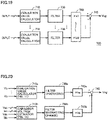
- Fig. 19 is a block diagram illustrating a configuration example of the voltage evaluator according to a fourth embodiment.
- voltage evaluation value generator 700 includes M (M is a natural number equal to or greater than 2) sets of evaluation value calculator 710 and filter 730 described in the third embodiment and further includes a gain multiplier 740 and an adder 745.
- Each of evaluation value calculators 710 is similar to any one of the first to seventh configuration examples shown in Fig. 9 to Fig. 15 as in the third embodiment.
- Abnormal value eliminator 720 shown in Fig. 16 may be arranged on the input side of evaluation value calculators 710.
- Filter 730 has predetermined characteristics in the same manner as in the third embodiment and allows the output value of evaluation value calculator 710 to pass through.
- the characteristics of a plurality of filters 730 may be different from each other or may be common among at least some of filters 730.
- Adder 745 adds M output values from gain multiplier 740.
- Voltage evaluation value generator 700 outputs the output value of adder 745 as voltage evaluation value Vcg to voltage macro controller 610.
- voltage evaluation value Vcg can be set appropriately by passing through filters 730 having different frequency characteristics and thereby adjusting the weight by gain ki.
- Fig. 20 is a block diagram illustrating a specific example of the voltage evaluator according to the fourth embodiment.
- voltage evaluation value generator 700 includes evaluation value calculator 710 shown in Fig. 11 , capacitor voltage estimator 717 shown in Fig. 14 , filters 730a and 730b, gain multipliers 740a and 740b, and an adder 745.
- evaluation value calculator 710 outputs (Vcmax+Vcmin)/2 in the same group (phase or arm).
- capacitor voltage estimator 717 outputs a capacitor voltage estimation value estimated from arm current Iarm in the same group (phase or arm).
- Filter 730a is configured to have the characteristic of averaging the successively generated output values of evaluation value calculator 710.
- filter 730a can be formed with, for example, a lowpass filter such as a first-order lag filter or a filter that calculates a moving average or an integral mean value.
- Filter 730b is configured to have the characteristic of extracting a change in capacitor voltage estimation value successively output from capacitor voltage estimator 717.
- filter 730b can be formed with, for example, a low frequency cutoff (high-pass) filter or a pseudo differential filter.
- Gain multiplier 740a outputs a multiplication value of an output value of filter 730a by a gain ka.
- Gain multiplier 740b outputs a multiplication value of an output value of filter 730b by a gain kb.
- Each of gains ka and kb is set in a range of 0 to 1.0.
- Adder 745 adds output values of gain multipliers 740a and 740b.
- Voltage evaluation value generator 700 outputs the output value of adder 745 as voltage evaluation value Vcg to voltage macro controller 610.
- evaluation value calculator 710 corresponds to an embodiment of "first evaluation value calculator”
- capacitor voltage estimator 717 corresponds to an embodiment of "second evaluation value calculator”
- filter 730a corresponds to an embodiment of "first filter”
- filter 730b corresponds to an embodiment of "second filter”.
- Gain ka corresponds to "first gain”
- gain kb corresponds to "second gain”.
- the calculation value of evaluation value calculator 710 (Fig. 11 ) based on detection of capacitor voltages Vc is passed through filter 730a (lowpass filter) to remove the influence of ripple voltage.
- the capacitor voltage estimation value that reflects the behavior of arm current Iarm by capacitor voltage estimator 717 is passed through filter 730b (low frequency cutoff filter) to extract a change in capacitor voltage Vc.
- Fig. 5 illustrates the control in which a control value (circulating current command value Izref or circulation control command value Vzp) in a minor loop for controlling circulating current is generated by voltage macro controller 610.
- a control value circulating current command value Izref or circulation control command value Vzp
- the control using voltage evaluation value Vcg is not limited to such an example. That is, voltage evaluation value Vcg described in the present embodiment may be set as a control target value in the control of the mean value of capacitor voltages Vc in all of converter cells 7 or a plurality of converter cells 7 in each group described above.
- circulation control command value Vzp for controlling deficiency and excess of stored energy between converter cells 7 is reflected in arm voltage command values krefp and krefn in command distributor 606.
- the control by circulation control command value Vzp is not limited to the example in Fig. 5 .
- deficiency and excess of stored energy between converter cells 7 can also be controlled by modulation of the carrier signal used in the PWM control in each individual cell controller 202.
- Fig. 21 is a block diagram illustrating another configuration example of the individual cell controller.
- individual cell controller 202 differs from the configuration in Fig. 5 in that circulation control command value Vzp in Fig. 5 is input to carrier generator 203.
- circulation control command value Vzp is not input to command distributor 606, and command distributor 606 generates arm voltage command values krefp and krefn without reflecting circulation control command value Vzp.
- circulation control command value Vzp is generated using voltage evaluation value Vcg (all voltage evaluation value Vcgall and group voltage evaluation value Vcgr), and a common value is input to respective individual cell controllers 202 of a plurality of converter cells 7 belonging to the same group (each phase leg circuit or each arm).
- carrier generator 203 generates carrier signal CS by modulating a carrier signal for phase shift PWM control in accordance with reference phase ⁇ i, similar to that in Fig. 5 , in accordance with circulation control command value Vzp.
- Gate signal generator 207 generates gate signal ga using PMW modulation signal Spwm in accordance with comparison between carrier signal CS from carrier generator 203 and cell voltage command value krefc, in the same manner as described in Fig. 5 .
- carrier signal CS is modulated in accordance with circulation control command value Vzp, so that the pulse width of PMW modulation signal Spwm (that is, gate signal ga) is controlled such that the difference between circulating current Iz and circulating current command value Izref in Fig. 5 is further reduced in accordance with circulation control command value Vzp, as illustrated in Fig. 22 and Fig. 23 .
- PMW modulation signal Spwm that is, gate signal ga
- Fig. 22 shows a conceptual waveform diagram illustrating base line modulation as a first example of carrier signal modulation.
- Fig. 23 shows a conceptual waveform diagram illustrating frequency modulation as a second example of carrier signal modulation.
- the modulation method of carrier signal CS is not limited to these methods. Any modulation method that can perform control such that the pulse width of the finally generated PMW modulation signal Spwm (that is, gate signal ga) changes in accordance with a circulating voltage command value (for example, the greater the circulation control command value Vpz is, the wider the pulse width of PMW modulation signal Spwm is).
- base line BL that is a reference potential of triangular carrier signal CS similar to that in Fig. 8 changes in accordance with circulation control command value Vpz.
- the waveform of arm voltage command value kref is the same between Fig. 8 and Fig. 22 .
- the signal waveforms are exaggerated for explanation and do not illustrate actual signal waveforms as they are, in the same manner as in Fig. 8 .
- the frequency of carrier signal CS changes in accordance with circulation control command value Vpz.
- a sawtooth pulse waveform is used as carrier signal CS.
- the waveform of each single pulse forming carrier signal CS is the same, but the frequency it is generated (that is, the frequency of carrier signal CS) changes in accordance with circulation command value Vpz.
- deficiency and excess of stored energy between converter cells 7 can also be controlled in accordance with circulation control command value Vzp generated using voltage evaluation value Vcg, even by the carrier signal modulation illustrated in Fig. 21 to Fig. 23 .
- circulation control command value Vpz may fail to be sufficiently reflected in arm voltage command value kref, in the control of reflecting circulation control command value Vpz in arm voltage command value kref as illustrated in Fig. 5 , due to the influence of quantization bit rate.
- the control by the carrier signal modulation can be expected to improve accuracy in control of circulating current.
- power converter 2 has a double star configuration and is mainly used for AC/DC converter for high voltage direct current (HVDC) transmission.
- HVDC high voltage direct current
- control of the power converter explained in the foregoing embodiments is applicable to power converters of any other configurations.
- control described in the present embodiments can be applied to power converter 2 having a single delta configuration.
- control described in the present embodiments can be applied to power converter 2 having a single star configuration.
Landscapes
- Engineering & Computer Science (AREA)
- Power Engineering (AREA)
- Inverter Devices (AREA)
Applications Claiming Priority (1)
| Application Number | Priority Date | Filing Date | Title |
|---|---|---|---|
| PCT/JP2019/047045 WO2021111502A1 (ja) | 2019-12-02 | 2019-12-02 | 電力変換装置 |
Publications (2)
| Publication Number | Publication Date |
|---|---|
| EP4071997A1 true EP4071997A1 (de) | 2022-10-12 |
| EP4071997A4 EP4071997A4 (de) | 2022-11-23 |
Family
ID=72745107
Family Applications (1)
| Application Number | Title | Priority Date | Filing Date |
|---|---|---|---|
| EP19955330.6A Pending EP4071997A4 (de) | 2019-12-02 | 2019-12-02 | Stromumwandlungsvorrichtung |
Country Status (4)
| Country | Link |
|---|---|
| US (1) | US12308763B2 (de) |
| EP (1) | EP4071997A4 (de) |
| JP (1) | JP6768993B1 (de) |
| WO (1) | WO2021111502A1 (de) |
Families Citing this family (5)
| Publication number | Priority date | Publication date | Assignee | Title |
|---|---|---|---|---|
| WO2021095141A1 (ja) * | 2019-11-12 | 2021-05-20 | 三菱電機株式会社 | 電力変換器の試験装置および試験方法 |
| WO2021159219A1 (en) * | 2020-02-14 | 2021-08-19 | Ecole De Technologie Superieure | Three-phase multilevel electric power converter |
| WO2021181583A1 (ja) * | 2020-03-11 | 2021-09-16 | 三菱電機株式会社 | 電力変換装置 |
| EP4354725A4 (de) * | 2021-06-10 | 2024-08-07 | Mitsubishi Electric Corporation | Leistungswandler |
| FR3126268A1 (fr) * | 2021-08-18 | 2023-02-24 | Safran Electronics & Defense | Système de conversion électrique de type multi niveaux protégé contre une surintensité électrique |
Family Cites Families (10)
| Publication number | Priority date | Publication date | Assignee | Title |
|---|---|---|---|---|
| DK2100366T3 (en) | 2006-12-08 | 2017-10-16 | Siemens Ag | Creating an equilibrium in active power of the phase modules of a converter |
| JP5455055B2 (ja) | 2010-02-26 | 2014-03-26 | 国立大学法人東京工業大学 | 電力変換器 |
| JP5721096B2 (ja) | 2010-08-23 | 2015-05-20 | 国立大学法人東京工業大学 | 電力変換器 |
| JP5894777B2 (ja) * | 2011-12-07 | 2016-03-30 | 株式会社日立製作所 | 電力変換装置 |
| US10356854B2 (en) * | 2013-12-19 | 2019-07-16 | Neturen Co., Ltd. | Power conversion apparatus and power conversion method |
| WO2018211624A1 (ja) | 2017-05-17 | 2018-11-22 | 三菱電機株式会社 | 電力変換装置 |
| JP6943184B2 (ja) * | 2017-09-06 | 2021-09-29 | 株式会社明電舎 | モジュラー・マルチレベル・カスケード変換器 |
| EP3739744B1 (de) | 2018-01-12 | 2024-11-06 | Mitsubishi Electric Corporation | Stromumwandlungsvorrichtung |
| JP6545425B1 (ja) * | 2018-12-25 | 2019-07-17 | 三菱電機株式会社 | 電力変換装置 |
| US12015354B2 (en) * | 2018-12-25 | 2024-06-18 | Mitsubishi Electric Corporation | Power conversion device capable of suppressing a harmonic component in an output voltage from an arm that increases after bypass of a failed converter cell |
-
2019
- 2019-12-02 US US17/774,990 patent/US12308763B2/en active Active
- 2019-12-02 WO PCT/JP2019/047045 patent/WO2021111502A1/ja not_active Ceased
- 2019-12-02 EP EP19955330.6A patent/EP4071997A4/de active Pending
- 2019-12-02 JP JP2020537019A patent/JP6768993B1/ja active Active
Also Published As
| Publication number | Publication date |
|---|---|
| JPWO2021111502A1 (ja) | 2021-12-02 |
| US20220393616A1 (en) | 2022-12-08 |
| WO2021111502A1 (ja) | 2021-06-10 |
| JP6768993B1 (ja) | 2020-10-14 |
| US12308763B2 (en) | 2025-05-20 |
| EP4071997A4 (de) | 2022-11-23 |
Similar Documents
| Publication | Publication Date | Title |
|---|---|---|
| US12308763B2 (en) | Power conversion device | |
| EP4030612B1 (de) | Stromumwandlungsvorrichtung | |
| US11750080B2 (en) | Power conversion device | |
| US12273045B2 (en) | Power conversion device with individual cell and arm balancing | |
| US12413156B2 (en) | Capacitor balancing control in an HVDC MMC | |
| EP3627684A1 (de) | Stromwandlungsvorrichtung | |
| EP3273586A1 (de) | Stromwandlungsvorrichtung | |
| US12562653B2 (en) | Power conversion device | |
| EP3905508B1 (de) | Stromumwandlungsvorrichtung | |
| EP4120540A1 (de) | Stromumwandlungsvorrichtung | |
| US12348127B2 (en) | Power conversion device | |
| US20260018991A1 (en) | Power conversion device and offshore wind power generation system | |
| EP4120543A1 (de) | Stromumwandlungsvorrichtung | |
| US20250070686A1 (en) | Power conversion device and control method for power conversion device | |
| US12218606B2 (en) | Power conversion device | |
| EP4262078A1 (de) | Leistungswandler | |
| JP7165037B2 (ja) | 電力変換装置および電力変換装置の制御方法 | |
| Tashakor et al. | Compensated state-space model of diode-clamped mmcs for sensorless voltage estimation | |
| JP7843947B1 (ja) | 電力変換装置 | |
| JP7130172B1 (ja) | 電力変換装置 | |
| EP4572067A1 (de) | Leistungsumwandlungssystem und steuerungsvorrichtung | |
| EP4641909A1 (de) | Leistungswandler | |
| EP4542842A1 (de) | Elektrische leistungsumwandlungsvorrichtung und steuerungsverfahren dafür | |
| EP4318926A1 (de) | Leistungswandler |
Legal Events
| Date | Code | Title | Description |
|---|---|---|---|
| STAA | Information on the status of an ep patent application or granted ep patent |
Free format text: STATUS: THE INTERNATIONAL PUBLICATION HAS BEEN MADE |
|
| PUAI | Public reference made under article 153(3) epc to a published international application that has entered the european phase |
Free format text: ORIGINAL CODE: 0009012 |
|
| STAA | Information on the status of an ep patent application or granted ep patent |
Free format text: STATUS: REQUEST FOR EXAMINATION WAS MADE |
|
| 17P | Request for examination filed |
Effective date: 20220429 |
|
| AK | Designated contracting states |
Kind code of ref document: A1 Designated state(s): AL AT BE BG CH CY CZ DE DK EE ES FI FR GB GR HR HU IE IS IT LI LT LU LV MC MK MT NL NO PL PT RO RS SE SI SK SM TR |
|
| A4 | Supplementary search report drawn up and despatched |
Effective date: 20221026 |
|
| RIC1 | Information provided on ipc code assigned before grant |
Ipc: H02M 7/483 20070101ALI20221020BHEP Ipc: H02M 7/48 20070101AFI20221020BHEP |
|
| DAV | Request for validation of the european patent (deleted) | ||
| DAX | Request for extension of the european patent (deleted) | ||
| STAA | Information on the status of an ep patent application or granted ep patent |
Free format text: STATUS: EXAMINATION IS IN PROGRESS |
|
| 17Q | First examination report despatched |
Effective date: 20230907 |