EP4057598B1 - Klappbares endgerät - Google Patents
Klappbares endgerät Download PDFInfo
- Publication number
- EP4057598B1 EP4057598B1 EP20894088.2A EP20894088A EP4057598B1 EP 4057598 B1 EP4057598 B1 EP 4057598B1 EP 20894088 A EP20894088 A EP 20894088A EP 4057598 B1 EP4057598 B1 EP 4057598B1
- Authority
- EP
- European Patent Office
- Prior art keywords
- housing
- wire
- printed circuit
- circuit board
- flexible printed
- Prior art date
- Legal status (The legal status is an assumption and is not a legal conclusion. Google has not performed a legal analysis and makes no representation as to the accuracy of the status listed.)
- Active
Links
Images




Classifications
-
- G—PHYSICS
- G06—COMPUTING OR CALCULATING; COUNTING
- G06F—ELECTRIC DIGITAL DATA PROCESSING
- G06F1/00—Details not covered by groups G06F3/00 - G06F13/00 and G06F21/00
- G06F1/16—Constructional details or arrangements
- G06F1/1613—Constructional details or arrangements for portable computers
- G06F1/1633—Constructional details or arrangements of portable computers not specific to the type of enclosures covered by groups G06F1/1615 - G06F1/1626
- G06F1/1637—Details related to the display arrangement, including those related to the mounting of the display in the housing
- G06F1/1652—Details related to the display arrangement, including those related to the mounting of the display in the housing the display being flexible, e.g. mimicking a sheet of paper, or rollable
-
- G—PHYSICS
- G06—COMPUTING OR CALCULATING; COUNTING
- G06F—ELECTRIC DIGITAL DATA PROCESSING
- G06F1/00—Details not covered by groups G06F3/00 - G06F13/00 and G06F21/00
- G06F1/16—Constructional details or arrangements
- G06F1/1613—Constructional details or arrangements for portable computers
- G06F1/1633—Constructional details or arrangements of portable computers not specific to the type of enclosures covered by groups G06F1/1615 - G06F1/1626
- G06F1/1675—Miscellaneous details related to the relative movement between the different enclosures or enclosure parts
- G06F1/1679—Miscellaneous details related to the relative movement between the different enclosures or enclosure parts for locking or maintaining the movable parts of the enclosure in a fixed position, e.g. latching mechanism at the edge of the display in a laptop or for the screen protective cover of a PDA
-
- G—PHYSICS
- G06—COMPUTING OR CALCULATING; COUNTING
- G06F—ELECTRIC DIGITAL DATA PROCESSING
- G06F1/00—Details not covered by groups G06F3/00 - G06F13/00 and G06F21/00
- G06F1/16—Constructional details or arrangements
- G06F1/1613—Constructional details or arrangements for portable computers
- G06F1/1633—Constructional details or arrangements of portable computers not specific to the type of enclosures covered by groups G06F1/1615 - G06F1/1626
- G06F1/1675—Miscellaneous details related to the relative movement between the different enclosures or enclosure parts
- G06F1/1683—Miscellaneous details related to the relative movement between the different enclosures or enclosure parts for the transmission of signal or power between the different housings, e.g. details of wired or wireless communication, passage of cabling
-
- G—PHYSICS
- G06—COMPUTING OR CALCULATING; COUNTING
- G06F—ELECTRIC DIGITAL DATA PROCESSING
- G06F1/00—Details not covered by groups G06F3/00 - G06F13/00 and G06F21/00
- G06F1/16—Constructional details or arrangements
- G06F1/18—Packaging or power distribution
- G06F1/181—Enclosures
-
- H—ELECTRICITY
- H04—ELECTRIC COMMUNICATION TECHNIQUE
- H04M—TELEPHONIC COMMUNICATION
- H04M1/00—Substation equipment, e.g. for use by subscribers
- H04M1/02—Constructional features of telephone sets
- H04M1/0202—Portable telephone sets, e.g. cordless phones, mobile phones or bar type handsets
- H04M1/0206—Portable telephones comprising a plurality of mechanically joined movable body parts, e.g. hinged housings
- H04M1/0208—Portable telephones comprising a plurality of mechanically joined movable body parts, e.g. hinged housings characterized by the relative motions of the body parts
- H04M1/0214—Foldable telephones, i.e. with body parts pivoting to an open position around an axis parallel to the plane they define in closed position
- H04M1/0216—Foldable in one direction, i.e. using a one degree of freedom hinge
-
- H—ELECTRICITY
- H04—ELECTRIC COMMUNICATION TECHNIQUE
- H04M—TELEPHONIC COMMUNICATION
- H04M1/00—Substation equipment, e.g. for use by subscribers
- H04M1/02—Constructional features of telephone sets
- H04M1/0202—Portable telephone sets, e.g. cordless phones, mobile phones or bar type handsets
- H04M1/026—Details of the structure or mounting of specific components
-
- H—ELECTRICITY
- H04—ELECTRIC COMMUNICATION TECHNIQUE
- H04M—TELEPHONIC COMMUNICATION
- H04M1/00—Substation equipment, e.g. for use by subscribers
- H04M1/02—Constructional features of telephone sets
- H04M1/0202—Portable telephone sets, e.g. cordless phones, mobile phones or bar type handsets
- H04M1/026—Details of the structure or mounting of specific components
- H04M1/0266—Details of the structure or mounting of specific components for a display module assembly
- H04M1/0268—Details of the structure or mounting of specific components for a display module assembly including a flexible display panel
-
- H—ELECTRICITY
- H04—ELECTRIC COMMUNICATION TECHNIQUE
- H04M—TELEPHONIC COMMUNICATION
- H04M1/00—Substation equipment, e.g. for use by subscribers
- H04M1/02—Constructional features of telephone sets
- H04M1/0202—Portable telephone sets, e.g. cordless phones, mobile phones or bar type handsets
- H04M1/026—Details of the structure or mounting of specific components
- H04M1/0277—Details of the structure or mounting of specific components for a printed circuit board assembly
Definitions
- This disclosure generally relates to the communication field, and the invention in particular relates to a foldable terminal device.
- a foldable technology well finds a compromise between miniaturization development of a base of a terminal device and large-screen development of a display screen.
- a foldable mobile phone After being folded, a foldable mobile phone has a same size as a conventional mobile phone, and can be conveniently carried.
- a screen When a screen is expanded, a screen with a very large display area can be obtained.
- a foldable terminal device has two housings, the two housings are connected by using a third housing, and a wire penetrates through an interior of the third housing and is connected to the two housings.
- the wire inside the third housing moves as the terminal device is folded and expanded. In the movement process, the wire is prone to scratch with another component, and consequently the wire is prone to wear.
- US2018/324964A1 discloses an electronic device which comprise a first housing including a first surface and a second surface facing in a direction opposite the first surface, a second housing including a third surface and a fourth surface facing in a direction opposite the third surface, a hinge disposed between the first housing and the second housing configured to provide rotational motion between the first housing and the second housing, and a flexible display disposed from the first surface of the first housing across the hinge to the third surface of the second housing, at least part of the flexible display configured to form a curved surface as the hinge structure is folded, wherein the hinge may include dual-axis hinges configured to provide a first rotational axis allowing the first housing to rotate about the second housing and a second rotational axis allowing the second housing to rotate about the first housing and slides coupled with the first housing and the second housing and configured to provide sliding motion perpendicular to a lengthwise direction of the first housing and the second housing.
- CN208609020U discloses a foldable electronics, comprising: rotary shaft rack, including bottom plate and the first side plate and the second side plate that are connected to bottom plate opposite sides, bottom plate, the first, second side plate enclose and set to form accommodation space; First shell and second shell can turn around bracing strut rotation; Flexible screen, including the first area, intermediate region and second area being wholely set, first area is arranged in conjunction with first shell, and second area is arranged in conjunction with second shell, and intermediate region corresponds to the bottom plate of rotary shaft rack; And guide member, it is set between the intermediate region of flexible screen and rotary shaft rack, for applying the guiding force towards the accommodation space of rotary shaft rack to intermediate region. In the initial stage that foldable electronic switches from unfolded state to folded state, guide member keeps the intermediate region stress of flexible screen clear, and then deforms flexible screen towards predetermined direction, avoids flexible screen impaired.
- US2015/233162A1 discloses a foldable display apparatus.
- the foldable display apparatus includes a flexible display panel, first body configured to support a left portion of a flexible display panel, and second body configured to support a right portion of the flexible display panel, first and second frames configured to surround portions of outlines of the first and second bodies, a hinge member configured to hinge-connect the first and second frames with each other in a foldable manner, and first and second supports having sides hinge-connected to the first and second frames, and configured to form an accommodation space in which a folded portion of the flexible display panel is folded to form a curvature at a first position at which the first and second bodies are folded, and to support the folded portion of the flexible display panel at a second position at which the first and second bodies are unfolded
- CN209390110U discloses a kind of electronic equipment, including first shell, second shell, third shell, flexible screen, first rotating shaft and the first RF transmit-receive circuit
- flexible screen includes sequentially connected first fixed area, folding region and the second fixed area, first fixed area is fixed on first shell, second fixed area is fixed on second shell, third shell includes the first side being oppositely arranged and second side, accommodating space is formed between first side and second side, first shell is rotationally connected with the first side by first rotating shaft, second shell is rotationally connected with second side, so that face accommodating space when being in flat at least partially in electronic equipment of folding region, folding region is contained in accommodating space when being in folded state at least partially in electronic equipment;
- First rotating shaft is equipped with the first irradiation unit, and the first RF transmit-receive circuit is set at least one of first shell, second shell and third shell, and the first RF transmit-receive circuit is electrically connected the first irradiation unit.
- CN106707577A discloses a display screen module and a terminal.
- the display screen module comprises a flexible circuit board, a display driving chip and an overall fixing part used for being matched with a middle frame fixing part on a terminal middle frame.
- fixation of the relative positions of the display screen module and the terminal middle frame can be achieved, it is guaranteed that the display screen module does not shift after the terminal is assembled, then the position of the display driving chip in the terminal is fixed.
- the object of the invention is to provide a foldable terminal device in which a wire of the foldable terminal device is fastened to a third housing, to reduce abrasion of the wire.
- the invention provides a foldable terminal device, including a first housing, a second housing, a third housing, a wire, and a wire fastening assembly.
- Two rotating shafts are respectively disposed at both ends of the third housing, one side of the third housing is connected to the first housing through the two rotating shafts, the other side of the third housing is connected to the second housing through the two rotating shafts, at least one of the first housing and the second housing is rotatably connected to the third housing, the third housing is a semi-closed housing, a non-closed area of the third housing is provided with an opening area, and the wire fastening assembly is disposed between the two rotating shafts of the third housing.
- the wire penetrates through an interior of the third housing through the opening area of the third housing, the wire is connected to the wire fastening assembly inside the third housing, and both ends of the wire are respectively connected to the first housing and the second housing.
- the wire fastening assembly includes a first magnetic component and a magnetic assembly, the first magnetic component is fixedly connected to the interior of the third housing, the magnetic assembly is connected to the wire, and the magnetic assembly is magnetically connected to the first magnetic component. Because the wire located in the third housing is fastened by using the wire fastening assembly, a degree of freedom of the wire in the third housing can be reduced, so that a movement amount of the wire in the third housing can be reduced, a degree of abrasion of the wire can be reduced, and there are less worn parts of the wire.
- the first magnetic component may be fixedly connected to the interior of the third housing 3 in advance.
- the wire is connected to the magnetic assembly, and the magnetic assembly connected to the wire penetrates into the third housing from the first opening. Because there is a magnetic adsorption force between the magnetic assembly and the first magnetic component, after being placed into the third housing 3, the magnetic assembly automatically adsorbs on the first magnetic component. Then, the other end of the wire penetrates out from the second opening. It can be learned that, in this operation process, automatic positioning of the magnetic assembly and the first magnetic component is implemented, and installation is relatively convenient.
- the magnetic assembly includes a second magnetic component.
- the second magnetic component is connected to the first magnetic component; and the wire is disposed between the first magnetic component and the second magnetic component.
- the wire may be clamped by using a magnetic adsorption force between the first magnetic component and the second magnetic component.
- the magnetic assembly further includes a support.
- the support is disposed between the second magnetic component and the first magnetic component.
- the wire includes a flexible printed circuit board, and the flexible printed circuit board is disposed between the support and the second magnetic component.
- the flexible printed circuit board is in contact with or connected to the support.
- the flexible printed circuit board is in contact with or connected to the second magnetic component.
- the wire includes a multilayer flexible printed circuit board, and the multilayer flexible printed circuit board is disposed between the support and the second magnetic component.
- the multilayer flexible printed circuit board satisfies one or more of the following content: Two adjacent layers of flexible printed circuit boards in the multilayer flexible printed circuit board are in contact (or referred to as movable contact) with each other.
- a flexible printed circuit board in the multilayer flexible printed circuit board that is in contact with the support is in contact (or referred to as movable contact) with or connected to the support.
- a flexible printed circuit board in the multilayer flexible printed circuit board that is in contact with the second magnetic component is in contact with or connected to the second magnetic component.
- the multilayer flexible printed circuit board in this embodiment of this application may be in contact (or referred to as movable contact), and do not need to be bonded by using an adhesive. This can avoid failure of the flexible printed circuit board caused by the adhesive, and improve reliability of the flexible printed circuit board.
- the flexible printed circuit board in the multilayer flexible printed circuit board that is in contact with the support is in contact with the support, the flexible printed circuit board can slide in a process of folding and expanding the terminal device. Therefore, if there is an assembly tolerance, the tolerance can be more easily absorbed, so that lengths of the flexible printed circuit boards on the left and right sides of the wire fastening assembly can be more optimized.
- the flexible printed circuit board in the multilayer flexible printed circuit board that is in contact with the second magnetic component when the flexible printed circuit board in the multilayer flexible printed circuit board that is in contact with the second magnetic component is in contact with the second magnetic component, the flexible printed circuit board can slide in the process of folding and expanding the terminal device. Therefore, if there is an assembly tolerance, the tolerance can be more easily absorbed, so that lengths of the flexible printed circuit boards on the left and right sides of the wire fastening assembly can be more optimized.
- the flexible printed circuit board in the multilayer flexible printed circuit board that is in contact with the second magnetic component is connected to the second magnetic component by using, for example, an adhesive or a double-sided tape, this can prevent the flexible printed circuit board from moving excessively unevenly on the left and right sides.
- the wire includes a cable, and the cable is disposed on a plane of the support that faces the second magnetic component, or the cable is disposed on a plane of the support that faces the first magnetic component.
- the flexible printed circuit board is disposed at one end of the support, and the cable is disposed at the other end of the support.
- a distance between a first contact area and a second contact area that are on the support is greater than a preset distance, the first contact area includes a contact area between the flexible printed circuit board and the support, and the second contact area includes a contact area between the cable and the support.
- an arc groove is disposed on the support, and the cable is clamped to the arc groove.
- a center of the arc groove faces an end away from the flexible printed circuit board.
- a bending direction of the cable is fixed by a shape of the groove. Therefore, in a process of folding the terminal device, a degree of bending freedom of the cable can be reduced, friction between the cable and another component of the third housing (for example, an inner surface or a bearing of the third housing) can be reduced, and friction between the cable and the flexible printed circuit board can be reduced.
- a fastener assembly is disposed on the support, the cable is clamped to the fastener assembly, the cable presents an arc in the fastener assembly, and a center of the arc presented by the cable in the fastener assembly faces the end away from the flexible printed circuit board.
- a bending direction of the cable is fixed by the fastener assembly. Therefore, in a process of folding the terminal device, a degree of bending freedom of the cable can be reduced, friction between the cable and another component of the third housing (for example, an inner surface or a bearing of the third housing) can be reduced, and friction between the cable and the flexible printed circuit board can be reduced.
- stop blocks are disposed on a surface of the support that faces the first magnetic component, and the stop blocks are disposed at both sides of the first magnetic component. In this way, when the magnetic assembly moves leftward or rightward, the stop blocks are blocked by the first magnetic component, so as to limit a movement amount of the magnetic assembly in a horizontal direction.
- the terminal device further includes: a buffer component, where the buffer component penetrates between the magnetic assembly and the third housing. In this way, friction and scratches between the wire and a first inner housing can be reduced.
- the buffer component presents a multidimensional wave shape. In this way, a redundancy of the wire inside the third housing can be better and more naturally absorbed when the terminal device is in the expanded state.
- a difference between a line length between the wire fastening assembly and the first housing and a line length between the wire fastening assembly and the second housing is within a preset range. In this way, the redundancy of the wire may be relatively evenly allocated to both sides of the wire fastening assembly.
- the wire includes the cable, and the cable is made by using a rubber in-mold decoration technology.
- a diameter of an area that is on the cable and connected to the third housing, the first housing, and the second housing is greater than a preset diameter.
- a positioning structure is disposed in the area that is on the cable and connected to the third housing, the first housing, and the second housing. In this way, the cable can be more accurately positioned to the support, the first housing, and the second housing, and a service life of the cable can be increased by increasing a diameter of a contact area between the cable and another component.
- an upper surface of the third housing includes a first inner housing, a second inner housing, and a third inner housing, and the upper surface of the third housing includes a surface on which a screen of the terminal device is laid; the second inner housing and the third inner housing are located at both sides of the first inner housing; one side of the second inner housing is rotatably connected to the first inner housing, and the other side is connected to the first inner housing; and one side of the third inner housing is rotatably connected to the first inner housing, and the other side is connected to the second inner housing.
- the first inner housing, the second inner housing, and the third inner housing may form relatively large space, to reserve specific space for a folded area of the screen, so that the screen can be in a natural state as much as possible.
- an embodiment of this application provides a foldable terminal device, including a first housing, a second housing, a third housing, a wire, a wire fastening assembly, and a buffer component.
- Two rotating shafts are respectively disposed at both ends of the third housing, one side of the third housing is connected to the first housing through the two rotating shafts, the other side of the third housing is connected to the second housing through the two rotating shafts, at least one of the first housing and the second housing is rotatably connected to the third housing, the third housing is a semi-closed housing, a non-closed area of the third housing is provided with an opening area, one side or a plurality of sides of the opening area is or are designed with a rounded corner, a diameter of the rounded corner is greater than a preset diameter, a wire fastening assembly is disposed between the two rotating shafts of the third housing, and a wire is fastened to the wire fastening assembly.
- An upper surface of the third housing includes a first inner housing, a second inner housing, and a third inner housing, and the upper surface of the third housing includes a surface on which a screen of the terminal device is laid; the second inner housing and the third inner housing are located at both sides of the first inner housing; one side of the second inner housing is rotatably connected to the first inner housing, and the other side is connected to the first housing; and one side of the third inner housing is rotatably connected to the first inner housing, and the other side is connected to the second housing.
- the wire includes a cable and a multilayer flexible printed circuit board.
- the wire penetrates through an interior of the third housing through the opening area of the third housing, both ends of the wire are respectively connected to the first housing and the second housing, the cable is made by using a rubber in-mold decoration technology, a diameter of an area that is on the cable and connected to the third housing, the first housing, and the second housing is greater than a preset diameter, and a positioning structure is disposed in the area that is on the cable and connected to the third housing, the first housing, and the second housing.
- the wire fastening assembly includes a first magnetic component, a second magnetic component, and a support.
- the first magnetic component is fixedly connected to the interior of the third housing.
- the second magnetic component is magnetically connected to the first magnetic component.
- the support is disposed between the second magnetic component and the first magnetic component. Stop blocks are disposed on a surface of the support that faces the first magnetic component, and the stop blocks are disposed at both sides of the first magnetic component.
- An arc groove is disposed on the support, the cable is clamped to the arc groove, and a center of the arc groove faces an end away from the multilayer flexible printed circuit board.
- a fastener assembly is disposed on the support, the cable is clamped to the fastener assembly, the cable presents an arc in the fastener assembly, and a center of the arc presented by the cable in the fastener assembly faces the end away from the multilayer flexible printed circuit board.
- the multilayer flexible printed circuit board is disposed at one end of the support, a multilayer cable is disposed at the other end of the support, a distance between a first contact area and a second contact area that are on the support is greater than a preset distance, the first contact area includes a contact area between the flexible printed circuit board and the support, and the second contact area includes a contact area between the cable and the support.
- the multilayer flexible printed circuit board is disposed between the support and the second magnetic component, two adjacent layers of flexible printed circuit boards in the multilayer flexible printed circuit board are in contact (or referred to as movable contact) with each other.
- a flexible printed circuit board in the multilayer flexible printed circuit board that is in contact with the support is in contact with or connected to the support.
- a flexible printed circuit board in the multilayer flexible printed circuit board that is in contact with the second magnetic component is in contact with or connected to the second magnetic component.
- the buffer component penetrates between the magnetic assembly and the third housing, and when the terminal device is in an expanded state, the buffer component presents a multidimensional wave shape.
- the first magnetic component 51 may be fixedly connected to the interior of the third housing 3 in advance.
- the wire is connected to the magnetic assembly, and the magnetic assembly connected to the wire penetrates into the third housing 3 from the first opening 31. Because there is a magnetic adsorption force between the magnetic assembly and the first magnetic component 51, after being placed into the third housing 3, the magnetic assembly automatically adsorbs on the first magnetic component 51.
- the other end of the wire penetrates out from the second opening 32. It can be learned that, in this operation process, automatic positioning of the magnetic assembly and the first magnetic component 51 is implemented, and installation is relatively convenient. Further, one side or a plurality of sides of the opening area is or are designed with the rounded corner, and the diameter of the rounded corner is greater than the preset diameter. This can make peripheries of the first opening and the second opening that are in contact with the wire smoother, thereby further reducing a degree of abrasion of the wire.
- a terminal device in embodiments of this application is a foldable device.
- the terminal device in embodiments of this application may include a device that provides a user with voice and/or data connectivity, for example, a handheld device with a wireless connection function, or a processing device connected to a wireless modem.
- the terminal device may communicate with a core network through a radio access network (radio access network, RAN), and exchange a voice and/or data with the RAN.
- radio access network radio access network
- the terminal device may include user equipment (user equipment, UE), a wireless terminal device, a mobile terminal device, a device-to-device (device-to-device, D2D) communication terminal device, a V2X terminal device, a machine-to-machine/machine-type communication (machine-to-machine/machine-type communication, M2M/MTC) terminal device, an internet of things (internet of things, IoT) terminal device, a subscriber unit (subscriber unit), a subscriber station (subscriber station), a mobile station (mobile station), a remote station (remote station), an access point (access point, AP), a remote terminal (remote terminal), an access terminal (access terminal), a user terminal (user terminal), a user agent (user agent), a user device (user device), or the like.
- IoT internet of things
- IoT internet of things
- IoT internet of things
- subscriber unit subscriber unit
- subscriber station subscriber station
- mobile station
- the terminal device may include a mobile phone (or referred to as a "cellular" phone), a computer with a mobile terminal device, or a portable, pocket-sized, handheld, or computer built-in mobile apparatus, for example, a device such as a personal communication service (personal communication service, PCS) phone, a cordless phone, a session initiation protocol (session initiation protocol, SIP) phone, a wireless local loop (wireless local loop, WLL) station, or a personal digital assistant (personal digital assistant, PDA).
- the terminal device further includes a limited device, for example, a device with low power consumption, a device with a limited storage capacity, or a device with a limited computing capability.
- the terminal device includes an information sensing device such as a barcode, radio frequency identification (radio frequency identification, RFID), a sensor, a global positioning system (global positioning system, GPS), or a laser scanner.
- FIG. 1a shows an example of a schematic diagram of a structure of a terminal device in a folded state according to an embodiment of this application.
- a screen of the terminal device may be folded.
- FIG. 1b shows an example of a schematic diagram of a structure of the terminal device in an expanded state according to this embodiment of this application.
- the screen is in an expanded state.
- one side that is of the terminal device in the expanded state and on which the screen is located is referred to as a screen side, and the other side opposite to the screen side is referred to as a housing side.
- FIG. 1b shows a schematic diagram of a structure of the housing side of the terminal device in the expanded state, that is, a schematic diagram of a structure of a side opposite to the screen side of the terminal device.
- the expanded state may also be referred to as an unfolded state.
- FIG. 1a when the terminal device is in the folded state, a part of a side surface of a third housing 3 is exposed (as shown in the figure, the part of the third housing 3 is exposed, and in actual application, another component may be used to block the exposed part of the third housing 3).
- FIG. 1b when the terminal device is in the expanded state, the third housing 3 on the housing side of the terminal device is blocked by a first housing 1 and a second housing 2 (in the figure, an example in which the third housing is completely blocked by the first housing 1 and the second housing 2 is used for illustration, and in actual application, when the terminal device is in the expanded state, the third housing 3 may not be completely blocked by the first housing 1 and the second housing 2).
- FIG. 1a when the terminal device is in the folded state, a part of a side surface of a third housing 3 is exposed (as shown in the figure, the part of the third housing 3 is exposed, and in actual application, another component may be used to block the exposed part of the third housing 3).
- FIG. 1b when
- the third housing 3 is indicated by using a dashed line. As shown in FIG. 1b , some first threaded holes 11 are further disposed on the third housing, and are configured to connect the third housing 3 to the first housing 1. Some second threaded holes 21 are disposed on the second housing 2, and are configured to connect the third housing 3 to the second housing 2.
- a component such as a battery cover or a small screen may be covered above a side that is of the third housing and on which the first threaded hole 11 and the second threaded hole 21 are disposed, and the covered component such as the battery cover or the small screen may block the first threaded hole 11 and the second threaded hole 21.
- FIG. 2a shows an example of a schematic diagram of a structure of the terminal device from which a part of the first housing 1 and a part of the second housing 2 in FIG. 1b are removed.
- the terminal device includes the first housing 1, the second housing 2, the third housing 3, the wire, and a wire fastening assembly 5.
- the wire is shown by using a flexible printed circuit board 41 and a cable 42 as an example.
- the wire may include the flexible printed circuit board 41 and/or the cable 42.
- two rotating shafts 33 may be respectively disposed at both ends of the third housing 3.
- the rotating shaft 33 is disposed inside the third housing 3, and is indicated by using a dashed line in FIG. 2a .
- One side of the third housing 3 may be connected to the first housing 1 through the rotating shaft 33, the other side of the third housing may be connected to the second housing 2 through the rotating shaft 33, and at least one of the first housing 1 and the second housing 2 is rotatably connected to the third housing 3 through the rotating shaft 33.
- a part of the first housing 1 and a part of the second housing 2 are removed in FIG. 2a .
- the third housing 3 may be a semi-closed housing.
- a non-closed area may be disposed on the side surface of the third housing 3.
- the non-closed area of the third housing 3 may be one or more opening areas.
- the opening area may be configured to enable the wire to penetrate through an interior of the third housing 3 during assembly of the terminal device.
- the wire penetrates through the interior of the third housing 3 through the opening area of the third housing 3, and both ends of the wire are respectively connected to circuit boards in the first housing 1 and the second housing 2.
- both ends of the wire may be respectively connected to a primary board and a secondary board (or an antenna) of the terminal device.
- the opening area of the third housing 3 may include a first opening 31 and a second opening 32.
- the first opening 31 and the second opening 32 may be disposed at a relatively middle position of the third housing 3, or may be adjusted based on a specific assembly situation of the wire.
- the wire In an assembly process, the wire needs to penetrate into the third housing 3 through the first opening 31 and penetrate out from the second opening 32.
- the wire may alternatively penetrate into the third housing 3 through the second opening 32 and penetrate out from the first opening 31.
- the wire may be configured to transfer a power supply, a signal, heat, and the like between the first housing 1 and the second housing 2.
- the wire may include the flexible printed circuit board 41 and/or the cable 42.
- the cable 42 may be a coaxial cable.
- the flexible printed circuit board 41 may be a flexible printed circuit (Flexible Printed Circuit, FPC). As shown in FIG. 2a , the flexible printed circuit board 41 may pass through the third housing 3 and be connected to both the first housing 1 and the second housing 2.
- the cable 42 may pass through the third housing 3 and is connected to both the first housing 1 and the second housing 2.
- the cable 42 is connected to the third housing 3 by using the wire fastening assembly 5.
- a part of the wire is blocked when passing through the third housing 3.
- parts of the cable 42 and the flexible printed circuit board 41 that are blocked by the third housing 3 are indicated by using dashed lines.
- the wire fastening assembly 5 may be disposed inside the third housing 3, for example, may be disposed between the rotating shafts at both ends of the third housing.
- the wire is connected to the wire fastening assembly 5.
- the wire fastening assembly 5 is indicated by using a dashed line in FIG. 2a .
- FIG. 2b is a schematic diagram of a structure of a terminal device obtained after the wire fastening assembly 5 in FIG. 2a is removed.
- a degree of freedom of the wire in the third housing 3 is relatively large, and a bending form of the wire is relatively random (in this embodiment of this application, the bending form of the wire may refer to a bending shape of the wire).
- friction or a scratch is prone to occur between the wire and the rotating shaft 33 in the third housing 3, a degree of abrasion is relatively severe, and there are a relatively large quantity of worn parts of the wire.
- the wire may be torn off in the process of folding the terminal device because the wire is stuck in the gap, and reliability of the wire is relatively low.
- the wire in the process of folding the terminal device, the wire may be pulled to one side, and in a process of folding the terminal device for a plurality of times, the wire may be torn off.
- an upper surface of an intermediate housing refers to a surface including a first inner housing 35, a second inner housing 351, and a third inner housing 352.
- the bending form of the wire may be limited within a specific range, for example, the wire is kept away from the gap on the side surface of the third housing 3 as far as possible. In this way, in the process of folding and expanding the terminal device, the wire is not stuck in the gap of the third housing 3 in the process of folding the terminal device, abrasion caused to the wire by the gap of the third housing 3 can be avoided, and reliability of the wire can be improved.
- the wire is fastened by using the wire fastening assembly 5, in the process of folding the terminal device, the wire is not likely to be excessively pulled, so that a possibility that the wire is torn off can be reduced, and reliability of the wire can be improved.
- the bending form of the wire is limited, relatively small space is needed in the cavity of the third housing 3 for the wire to move, which can lay a foundation for miniaturization development of the terminal device.
- the bending form of the wire is relatively fixed, and activity space of the redundancy does not need to be relatively large. Therefore, the hole on the upper surface of the third housing 3 can be avoided, and sinking of the flexible display due to the hole can be avoided.
- a length of a wire between the wire fastening assembly 5 and the first housing 1 may be controlled, and a length of a wire between the wire fastening assembly 5 and the second housing 2 may be controlled.
- the length of the wire that is between the wire fastening assembly 5 and the first housing 1 and that is located inside the third housing 3 is referred to as a first length
- the length of the wire that is between the wire fastening assembly 5 and the second housing 2 and that is located inside the third housing 3 is referred to as a second length.
- the first length and the second length are controlled by using the wire fastening assembly 5, and do not change greatly in the process of expanding and folding the terminal device.
- this embodiment of this application provides an optional implementation.
- a difference between a line length of the wire between the wire fastening assembly 5 and the first housing 1 and a line length of the wire between the wire fastening assembly 5 and the second housing 2 is within a preset range.
- a difference between the first length and the second length is within a preset range.
- the wire fastening assembly 5 basically fastens a middle position of the wire located inside the third housing 3.
- the redundancy of the wire may be relatively evenly allocated to both sides of the wire fastening assembly 5, so that a difference between line lengths of both sides of the wire fastening assembly 5 can be reduced, and abrasion of wires on both sides of the wire fastening assembly 5 can be balanced. This avoids excessive abrasion of one side of the wire fastening assembly 5, and improves reliability of the wire.
- the wire penetrates through the first opening 31 of the third housing 3 and penetrates out from the second opening 32, and is fastened to the third housing 3 by using the wire fastening assembly 5.
- a size of the third housing 3 of the terminal device is usually relatively small, for example, a thickness size of the third housing 3 may be 5 millimeters or 6 millimeters. That is, operable space of the third housing 3 is very small. Therefore, the foregoing operation is technically difficult. To resolve this problem, this embodiment of this application provides a possible implementation. The following provides detailed descriptions.
- FIG. 3a is a schematic cross-sectional view in a direction D in FIG. 2a .
- FIG. 3a is a schematic diagram of a structure of an end surface of a middle part of the third housing.
- the wire fastening assembly 5 may include a first magnetic component 51 and a magnetic assembly.
- the first magnetic component 51 is fixedly connected to the interior of the third housing 3.
- the magnetic assembly is connected to the wire.
- the magnetic assembly may include a second magnetic component 54.
- the first magnetic component 51 may be fixedly connected to the interior of the third housing 3 in advance.
- specific operations are as follows: The wire is connected to the magnetic assembly, and the magnetic assembly connected to the wire penetrates into the third housing 3 from the first opening 31. Because there is a magnetic adsorption force between the magnetic assembly and the first magnetic component 51, after being placed into the third housing 3, the magnetic assembly automatically adsorbs on the first magnetic component 51. Then, the other end of the wire penetrates out from the second opening 32. It can be learned that, in this operation process, an assembler fastens the wire to the magnetic assembly, and penetrates the magnetic assembly connected to the wire into the third housing 3.
- the magnetic assembly is adsorbed by the magnetic adsorption force of the first magnetic component 51, so that the magnetic assembly and the first magnetic component 51 are automatically positioned.
- the magnetic assembly connected to the wire is also adsorbed by the magnetic adsorption force to the first magnetic component 51, so that the magnetic assembly can be automatically positioned.
- This implementation can prevent expanding the size of the third housing 3 for ease of assembly.
- automatic positioning can be implemented in a process of penetrating the wire into the third housing 3, other parts except the opening area of the third housing 3, for example, the rotating shaft 33 and both ends of the third housing 3, can be closed, and a size of a semi-closed third housing 3 can be further reduced. This provides technical support for a thinner terminal device.
- the magnetic assembly may not include a support 53 (the implementation is not shown in the accompanying drawings).
- the second magnetic component 54 may be magnetically connected to the first magnetic component 51.
- the second magnetic component 54 may be provided with a groove 531 or another structure that can fasten the wire, so that the wire is fastened by using the groove 531 or the structure that fastens the wire and that is disposed on the second magnetic component 54.
- the second magnetic component 54 may not be provided with the groove 531 or another structure that can fasten the wire, the wire directly penetrates between the first magnetic component 51 and the second magnetic component 54, and the wire is clamped by using a magnetic adsorption force between the first magnetic component 51 and the second magnetic component 54.
- the magnetic assembly inside the third housing 3 may include the support 53 and the second magnetic component 54.
- the support 53 is disposed between the first magnetic component 51 and the second magnetic component 54.
- the intermediate housing may include an outer housing 34, the first inner housing 35, the second inner housing 351, and the third inner housing 352.
- a lower surface of the third housing 3 includes the outer housing 34
- an upper surface of the third housing includes the first inner housing 35, the second inner housing 351, and the third inner housing 352.
- housings on a side of the third housing 3 that is relatively close to the screen are referred to as the first inner housing 35, the second inner housing 351, and the third inner housing 352, and a housing on a side that is relatively far away from the screen is referred to as the outer housing 34.
- the outer housing 34 names of the outer housing 34, the first inner housing 35, the second inner housing 351, and the third inner housing 352 are merely used for differentiation, and have no other actual limitation meanings.
- the third housing 3 is provided with a rotating shaft, and the rotating shaft is used to connect the first housing 1 and the second housing 2.
- the third housing 3 may also be commonly referred to as a rotating shaft
- the outer housing 34 may also be referred to as an outer shaft
- the first inner housing 35 may also be referred to as a first inner shaft
- the second inner housing 351 may also be referred to as a second inner shaft
- the third inner housing 352 may also be referred to as a third inner shaft.
- the wire penetrates into the third housing 3 from the first opening 31, and penetrates out of the third housing 3 from the second opening 32. Friction occurs between the wire and edges of the first opening 31 and the second opening 32. It can be seen from FIG. 3a that peripheries of the first opening 31 area and the second opening 32 area also limit the wire.
- rounding is performed on peripheries of the first opening 31 and the second opening 32. Rounding may be performed on all peripheries of the first opening 31 and the second opening 32, or rounding may be performed on some peripheries of the first opening 31 and the second opening 32. For example, rounding is performed on a side that is of the first opening 31 and in a direction parallel to a center line of the third housing 3.
- a diameter of rounding may be set to be larger, for example, may be greater than 1.5 millimeters.
- peripheries of the first opening 31 and the second opening 32 that are in contact with the wire are smoother, so that abrasion on the wire can be further reduced.
- the peripheries of the first opening 31 area and the second opening 32 area also limit the wire, when the terminal device is in the expanded state, the wire inside the third housing 3 can maintain a specific arc, thereby further limiting a bending form.
- FIG. 3b is an exploded view of an internal structure of a third housing of a terminal device according to an embodiment of this application.
- an internal structure of an intermediate housing area of the terminal device can be seen more clearly in a form of the exploded view, and a structure form of the outer housing 34 of the intermediate housing can be seen from FIG. 3b .
- the outer housing is an arc-shaped housing, and an opening area is disposed in a middle part.
- the second opening 32 disposed in a middle position of the outer housing 34 can be clearly seen in FIG. 3b .
- the first opening 31 is located at a position symmetrical to the second opening 32, and is not shown in FIG. 3b .
- the flexible printed circuit board 41 when the wire includes the flexible printed circuit board 41, the flexible printed circuit board 41 may be disposed between the support 53 and the second magnetic component 54.
- the cable 42 When the wire includes the cable 42, the cable 42 may be connected to the support 53.
- the groove 531 (for example, the groove 531 of the support 53 in FIG. 3f below) may be disposed on the support 53 to clamp the cable 42.
- the cable 42 may be fastened to a surface of the support 53 that faces the first magnetic component 51, or may be fastened to a surface of the support 53 that faces the second magnetic component 54.
- a material of a magnetic component for example, the first magnetic component 51 and the second magnetic component 54
- a material of a magnetic component in this embodiment of this application may be a soft magnetic material, and a magnetic force of the magnetic component may be adjusted based on a requirement.
- the first magnetic component 51 may be a rectangular magnetic component.
- a shape of the first magnetic component may be set freely, for example, may be set to an irregular shape.
- a buffer component has a specific width, for example, may be a wavy film with a specific width, penetrates through the intermediate housing, and is located between the support and the first inner housing 35, to provide buffer protection for the wire.
- FIG. 3c is a schematic diagram of a structure obtained after the outer housing and the first magnetic component 51 in FIG. 3b are removed.
- FIG. 3c also shows a structural form of a connection between the flexible printed circuit board penetrating inside the intermediate housing and the first housing and the second housing. As shown in FIG. 3c , one side of the flexible printed circuit board is laid on the first housing 1, and the other side is laid on the second housing 2.
- FIG. 3d is a partial enlarged diagram of an area A in FIG. 3c .
- Arrangement of the cable and the flexible printed circuit board on the support can be seen from FIG. 3d .
- the cable and the flexible printed circuit board may be arranged at two ends of the support.
- a distance between a first contact area 536 and a second contact area 537 that are on the support 53 is greater than a preset distance
- the first contact area 536 includes a contact area between the flexible printed circuit board 41 and the support 53
- the second contact area 537 includes a contact area between the cable 42 and the support 53.
- the first contact area 536 may be a contact area between the support 53 and a side of the flexible printed circuit board 41 that is relatively close to the cable 42
- the second contact area 537 may be a contact area between the support 53 and a position that is on the cable 42 and that is relatively close to the flexible printed circuit board 41.
- a distance between the first contact area 536 and the second contact area 537 on the support 53 may be a shortest distance between the flexible printed circuit board 41 and the cable 42 on the support 53.
- the preset distance may be determined based on experience, for example, may be set to 2 millimeters or 3 millimeters.
- friction between the cable 42 and the flexible printed circuit board 41 in a bending process can be further reduced.
- the cable 42 presents a W-shaped wave, and a bending radius of the cable 42 is relatively large. This can reduce a fatigue degree of the cable 42, and increase a service life of the cable 42.
- FIG. 3c it can be seen from FIG. 3c that the flexible printed circuit board 41 presents a W-shaped wave, and a bending radius of the flexible printed circuit board 41 is relatively large. This can reduce a fatigue degree of the flexible printed circuit board 41, and increase a service life of the flexible printed circuit board 41.
- FIG. 3e is a view shown in a direction B in FIG. 3c .
- a structural form of another end of the support can be seen.
- the another end of the support may be aligned with an end surface of the flexible printed circuit board.
- the another end of the support may also be slightly longer than the flexible printed circuit board, so that the support can span the entire flexible printed circuit board, to provide more protection for the flexible printed circuit board.
- a buffer component 6 is disposed between the second magnetic component 54 and the third housing 3.
- the buffer component 6 is laid between the wire and the first inner housing 35, to reduce friction and scratches between the wire and the first inner housing 35.
- a width of the buffer component 6 located inside the intermediate housing is greater than a width of the flexible printed circuit board 41 located inside the intermediate housing, so that the buffer component 6 can provide better protection for the flexible printed circuit board 41 located inside the intermediate housing.
- the buffer component 6 is stretched in a process of folding the terminal device, and is compressed inside the third housing 3 in a process of expanding the terminal device.
- the buffer component 6 may be a film having a specific width.
- the width of the buffer component 6 refers to a size of the buffer component 6 in a direction parallel to the center line of the third housing 3.
- the width of the buffer component 6 may be greater than a size of an area occupied by the wire in the direction parallel to the center line of the third housing 3. In this way, when the wire is bent, the buffer component 6 can better protect the wire.
- the wire in the third housing 3 When the terminal device is in the folded state, the wire in the third housing 3 is stretched, and a length of the wire in the third housing 3 of the terminal device in the folded state is L1.
- the wire in the third housing 3 When the terminal device is in the expanded state, the wire in the third housing 3 is bent and retracted in the third housing 3.
- a length of the wire in the third housing 3 of the terminal device in the expanded state is L2.
- L1 is greater than L2. That is, a length of the wire of the third housing 3 needs to be at least greater than L1, and when the terminal device is in the expanded state, at least a wire segment of a length (L1-L2) is bent inside the third housing 3 as a redundancy.
- the buffer component 6 may be set to the wave shape shown in FIG.
- the buffer component 6 presents a multidimensional curve state. In other words, when the terminal device is in the expanded state, the buffer component 6 presents a wave shape. In this way, the redundancy of the wire inside the third housing 3 can be better and more naturally absorbed when the terminal device is in the expanded state. In addition, because the buffer component 6 is in a wave shape, in the process of expanding and folding the terminal device, a redundancy of the buffer component 6 may also move in the third housing 3 in a preset form.
- the buffer component 6 may be a wave-shaped film made of a flexible material such as a polyimide film (polyimide film), Mylar (Mylar), polyethylene terephthalate (polyethylene terephthalate, PET), or rubber (rubber).
- a heat dissipation material for example, graphite may be added to the buffer component 6, so that heat of the first housing 1 and the second housing 2 is conducted by using the buffer component 6, to balance temperatures of the first housing 1 and the second housing 2.
- FIG. 3f is a schematic diagram of a structure of the support 53 in FIG. 3b .
- a structure of a support may be a mechanical part having a groove.
- FIG. 3f shows an arc structure of the groove 531 on the support 53.
- a side of the groove may be set to a sawtooth shape.
- the flexible printed circuit board 41 and the cable 42 may be located at two ends of the support 53, as shown in FIG.
- a center of the groove 531 that is on the support 53 and that is used to clamp the cable 42 may face a side away from the flexible printed circuit board 41.
- the groove 531 has a specific angle, after the cable 42 is fastened in the groove 531, a bending direction of the cable 42 is fixed by a shape of the groove 531. Therefore, in a process of folding the terminal device, a degree of bending freedom of the cable 42 can be reduced, friction between the cable 42 and another component of the third housing 3 (for example, an inner surface or a bearing of the third housing 3) can be reduced, and friction generated by the cable 42 can also be reduced. Further, because the center of the groove 531 faces the end away from the flexible printed circuit board 41, friction between the cable 42 and the flexible printed circuit board 41 can be reduced in a bending process of the cable 42.
- a groove is disposed on a first surface 540 of the support (the first surface of the support is a surface of the support that is relatively far away from the screen), to place the cable, and the flexible printed circuit board is placed on a second surface of the support (the second surface of the support is a surface of the support that is relatively close to the screen; in FIG. 3f , because the second surface is opposite to the first surface 540, the second surface cannot be seen in FIG. 3f , and therefore the second surface is not shown in FIG. 3f ).
- a step structure 538 may be disposed on the second surface of the support, to reduce displacement of the flexible printed circuit board towards the cable, so as to reduce friction between the cable and the flexible printed circuit board support.
- the support 53 further includes stop blocks 535.
- the stop blocks 535 may be disposed on a surface of the support 53 that faces the first magnetic component 51, and the stop blocks 535 may be disposed at two sides of the support 53.
- the stop blocks 535 may be some protruding structural blocks disposed at two sides of the support 53.
- the stop blocks 535 are located at two sides of the first magnetic component 51. When the magnetic assembly moves leftward or rightward, the stop blocks 535 are blocked by the first magnetic component 51, so as to limit a movement amount of the magnetic assembly in a horizontal direction.
- a movement amount of the wire in the horizontal direction shown in FIG. 3a may be limited. This can alleviate a problem that the wire moves a lot in the horizontal direction caused by pulling the wire in the process of folding the terminal device, and further stabilize a form of the wire inside the third housing 3.
- the horizontal direction mentioned in this embodiment of this application is a direction perpendicular to the center line of the third housing 3 on a plane formed by a screen 12 when the terminal device is in the expanded state.
- FIG. 3b to FIG. 3f are described by using an example in which the groove 531 is disposed on the support 53.
- a structure used to fasten the cable 42 on the support 53 may be set as a fastener assembly.
- FIG. 3g to FIG. 3k an example in which a structure used to fasten the cable 42 on the support 53 in FIG. 2a is a fastener assembly is used for illustration, and detailed description is provided below.
- FIG. 3g is an exploded view of an internal structure of a third housing of another terminal device according to an embodiment of this application.
- an internal structure of an intermediate housing area of the terminal device can be seen more clearly in a form of the exploded view.
- the fastener assembly of the support 53 includes two parts, which are respectively a fastener 533 and a hole 534.
- a structural form that a cable is placed on a hole can be seen from FIG. 3g .
- the fastener 533 is not clamped to the hole 534.
- the hole 534 may be a rectangular hole, and the fastener 533 may be a mechanical part with ears at both ends.
- FIG. 3h is a schematic diagram of a structure in a direction C obtained after an outer housing, the first magnetic component 51, and the buffer component 6 in FIG. 3g are removed. That is, FIG. 3h is a schematic diagram of a structure of a rear side of the support. A rear side structure of the fastener and a rear side structure of the support can be seen from FIG. 3h . As shown in FIG. 3h , a flexible printed circuit board is laid on the rear side of the support, and a tail end of the support (the tail end of the support refers to an opposite end of an end at which the hole is disposed) slightly exceeds a width of the flexible printed circuit board. This can provide more protection for the flexible printed circuit board.
- the cable 42 when the cable 42 is fastened to the fastener assembly of the support 53, the cable 42 may be fastened to the fastener assembly in an arc angle.
- the flexible printed circuit board 41 and the cable 42 are located at two ends of the support 53, and a center of the arc of the cable 42 may face a side away from the flexible printed circuit board 41. In this way, because the cable 42 has a specific angle, after the cable 42 is fastened to the fastener assembly, a bending direction of the cable 42 is fixed.
- a degree of bending freedom of the cable 42 can be reduced, friction between the cable 42 and another component of the third housing 3 (for example, an inner surface or a bearing of the third housing 3) can be reduced, and friction generated by the cable 42 can also be reduced. Further, because the center of the arc of the cable 42 faces the end away from the flexible printed circuit board 41, friction between the cable 42 and the flexible printed circuit board 41 can be reduced in a bending process of the cable 42. In addition, a distance between the fastener assembly of the support 53 and the flexible printed circuit board 41 fastened on the support 53 may be increased.
- the groove 531 and the fastener assembly that are used to fasten the cable 42 are merely two examples.
- another structure that can fasten the cable 42 may also be disposed on the support 53.
- FIG. 3i is a schematic diagram of a structure obtained after the fastener 533 is clamped to the hole 534.
- the cable 42 is placed on the hole 534, and the fastener 533 is clamped to the hole 534, so that the cable 42 is clamped.
- FIG. 3i shows a structural form after the fastener 533 is clamped to the hole 534, and ears on two sides of the fastener 533 may be inserted into the hole 533, so that the fastener 533 is clamped to the hole 534.
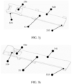
- FIG. 3j is a schematic diagram of a structure of the support 53 in FIG. 3g .
- the stop blocks 535 are disposed on the first surface 540 (the first surface 540 is a surface that is relatively close to the first magnetic component) of the support.
- the stop blocks 535 refer to the foregoing content. Details are not described herein again.
- FIG. 3k is a schematic diagram of a structure of the support 53 in a direction C in FIG. 3g .
- a structural form of a second surface 541 of the support can be seen from FIG. 3k .
- one end of the support 53 is provided with the hole, and an arc-shaped boss structure 539 may be provided at the end provided with the hole.
- a center of the arc-shaped boss structure 539 faces one end away from the flexible printed circuit board 41.
- FIG. 3l is a schematic diagram of a structure of a screen side in FIG. 2a .
- a screen side of the third housing 3 includes the first inner housing 35, the second inner housing 351, and the third inner housing 352.
- the first inner housing 35 is rotatably connected to the second inner housing 351, and the first inner housing 35 is rotatably connected to the third inner housing 351.
- the second inner housing 351 and the third inner housing 352 are respectively disposed at both sides of the first inner housing 35.
- the second inner housing 351 is connected to the first housing 1, and the third inner housing 352 is connected to the second housing 2.
- the buffer component 6 penetrates inside the third housing, and is laid in the first housing 1 and the second housing 2.
- the screen 12 is further laid on the first inner housing 35, the second inner housing 351, the third inner housing 352, and the buffer component of the third housing.
- FIG. 3m is a schematic diagram of a structure of the terminal device in FIG. 3m in a folded state.
- the first inner housing 35, the second inner housing 351, and the third inner housing 352 may form relatively large space, to reserve specific space for a folded area of the screen 12, so that the screen 12 can be in a natural state as much as possible.
- FIG. 3n is a schematic diagram of a structure of another terminal device in a folded state. It can be seen from FIG. 3n that, if only one first inner housing 35 is disposed on the third housing, the first inner housing 35 is directly connected to the first housing 1 and the second housing 2, and the second inner housing 351 and the third inner housing 352 are no longer disposed. It can be seen from FIG. 3n that, when the terminal device is in the folded state, space reserved by the first inner housing 35, the first housing 1, and the second housing 2 in the folded area of the screen 12 is relatively small, and the first housing 1 and the second housing 2 are prone to squeeze onto the screen 12. In this solution, a damage rate of the screen 12 is relatively high. In the solutions provided in this embodiment of this application shown in FIG.
- One end of the wire may be fastened to the first housing 1, and the other end of the wire may be fastened to the second housing 2.
- the wire may be fastened in a plurality of manners.
- a manner in which the wire is fastened to the first housing 1 is used as an example.
- a steel sheet 7 is fastened between the flexible printed circuit board 41 and the first housing 1, foam 8 and a presser 9 are placed on a top surface of the flexible printed circuit board 41 at a time, and the presser 9 is configured to press the flexible printed circuit board 41 tightly.
- the presser 9, the foam 8, the flexible printed circuit board 41, and the steel sheet 7 may be fastened to the first housing 1 by using screws or the like.
- a double-sided tape may be placed between the steel sheet 7 and the first housing 1, to further fasten the steel sheet 7 and play a buffering role.
- the foam 8 is configured to reduce abrasion between the wire and the presser 9, and plays a buffering role.
- a positioning hole may be preset on the first housing 1, and is configured to play a positioning role in a process of fastening the flexible printed circuit board 41 to the first housing 1. In other words, the positioning hole is configured to insert a fastening connector such as a screw.
- the cable 42 when the wire includes the cable 42, the cable 42 may be disposed between the steel sheet 7 and the presser 9, and the cable 42 disposed between the steel sheet 7 and the presser 9 is fastened to the first housing 1. Further, the presser 9, the cable 42, and the steel sheet 7 may be fastened to the first housing 1 by using screws or the like.
- the foam 8 may be disposed between the steel sheet 7 and the cable 42 for buffering. In this embodiment of this application, the foam 8 may alternatively be replaced with another rubber buffer material.
- a double-sided tape may be disposed between the steel sheet 7 and the first housing 1, to further fasten the steel sheet 7 and play a buffering role.
- the cable groove 531 may also be disposed on the first housing 1, and the cable groove 531 may be optionally disposed in an oblique direction, to match a bending form of the arc-shaped cable 42 fastened to the third housing 3.
- the cable 42 is fastened in the oblique cable groove 531, and the cable 42 may be glued to the oblique cable groove 531 through glue dispensing.
- a direction of the cable 42 fastened in the oblique cable groove 531 matches an arc shape of the cable 42 fastened by the support 53, so that the cable 42 is bent more naturally, abrasion of the cable 42 is reduced, and reliability of the cable 42 is further improved.
- the first housing 1 is used as an example for description.
- the wire is also fastened on the first housing 1 and the second housing 2, that is, on both sides of the third housing 3. Therefore, the degree of freedom of the wire may be further limited, a movement form of the wire may be further limited, and abrasion between the wire and the third housing 3 is further reduced.
- the wire may include one or more cables.
- one or more grooves may be disposed on the support, and a plurality of cables may be placed into one groove, or a plurality of cables may be placed into a plurality of grooves.
- one or more cables may be placed into one groove.
- one or more fastener assemblies may be disposed on the support. A plurality of cables are fastened by using the one or more fastener assemblies, and one fastener assembly may fasten one or more cables.
- the flexible printed circuit board included in the wire may be a single-layer flexible printed circuit board, or may include a multilayer flexible printed circuit board. That is, one or more layers of flexible printed circuit boards 41 may be included between the support 53 and the second magnetic component 54.
- the wire includes a single-layer flexible printed circuit board 41
- the flexible printed circuit board is disposed between the support and the second magnetic component. Because the flexible printed circuit board 41 is clamped between the support 53 and the second magnetic component 54 under an effect of a magnetic adsorption force between the second magnetic component 54 and the first magnetic component 51, the flexible printed circuit board 41 may be in movable contact with the support 53. In this way, in the process of folding and expanding the terminal device, relative movement may exist between the flexible printed circuit board and the support. In this way, if there is an assembly tolerance, the structural form more easily absorbs the tolerance, so that lengths of the flexible printed circuit boards 41 on the left and right sides of the wire fastening assembly 5 can be more optimized.
- the flexible printed circuit board 41 is in movable contact with the second magnetic component 54.
- relative movement may exist between the flexible printed circuit board and the second magnetic component.
- the structural form more easily absorbs the tolerance, so that lengths of the flexible printed circuit boards 41 on the left and right sides of the wire fastening assembly 5 can be more optimized.
- the flexible printed circuit board included in the wire may be a single-layer flexible printed circuit board, or may include a multilayer flexible printed circuit board. That is, one or more layers of flexible printed circuit boards 41 may be included between the support 53 and the second magnetic component 54.
- the wire includes a single-layer flexible printed circuit board 41
- the flexible printed circuit board is disposed between the support and the second magnetic component. Because the flexible printed circuit board 41 is clamped between the support 53 and the second magnetic component 54 under an effect of a magnetic adsorption force between the second magnetic component 54 and the first magnetic component 51, the flexible printed circuit board 41 may be connected to the support 53 by using, for example, an adhesive or a double-sided tape. In this way, in the process of folding and expanding the terminal device, the flexible printed circuit board and the support, and the flexible printed circuit board and the second magnetic component are adhered to each other by using the adhesive, and therefore are relatively evenly distributed on two sides.
- the flexible printed circuit board 41 is connected to the second magnetic component 54 by using, for example, the adhesive or the double-sided tape.
- the flexible printed circuit board and the support, and the flexible printed circuit board and the second magnetic component are adhered to each other by using the adhesive, and therefore are relatively evenly distributed on two sides.
- any two layers of the multilayer flexible printed circuit board 41 may be in movable contact. In other words, there may be relative displacement between any two layers of the flexible printed circuit board 41, and relative movement may exist in the process of folding and expanding the terminal device.
- the multilayer flexible printed circuit boards 41 are fixedly connected by using the adhesive, the multilayer flexible printed circuit boards 41 that are bonded are relatively hard and thick. In this case, the multilayer flexible printed circuit boards 41 are prone to be broken and fail.
- the multilayer flexible printed circuit boards 41 are in movable contact with each other and do not need to be bonded by using the adhesive. In this way, a failure of the flexible printed circuit board 41 caused by the adhesive can be avoided, and reliability of the flexible printed circuit board 41 can be improved.
- the second magnetic component 54 and the flexible printed circuit board 41 that is in contact with the second magnetic component 54 may be in movable contact, and may have relative displacement. Relative movement may exist in the process of folding and expanding the terminal device. In this way, the flexible printed circuit board 41 can slide in the process of folding and expanding the terminal device. Therefore, if there is an assembly tolerance, the tolerance can be more easily absorbed, so that lengths of the flexible printed circuit boards 41 on the left and right sides of the wire fastening assembly 5 can be more optimized.
- the second magnetic component 54 may be connected, by using, for example, an adhesive, to the flexible printed circuit board 41 that is in contact with the second magnetic component 54. In this way, quantities on two sides of the flexible printed circuit board can be kept relatively even.
- the support 53 and the flexible printed circuit board 41 that is in contact with the support 53 may be in movable contact, and may have relative displacement. Relative movement may exist in the process of folding and expanding the terminal device. In this way, the flexible printed circuit board 41 can slide in the process of folding and expanding the terminal device. Therefore, if there is an assembly tolerance, the tolerance can be more easily absorbed, so that lengths of the flexible printed circuit boards 41 on the left and right sides of the wire fastening assembly 5 can be more optimized.
- the support 53 and the flexible printed circuit board 41 that is in contact with the support 53 may be connected by using, for example, the adhesive.
- quantities on two sides of the flexible printed circuit board can be kept relatively even.
- FIG. 4a shows an example of a schematic diagram of a structure of a cable 42
- FIG. 4b shows an example of a schematic diagram of a structure of another cable 42
- the cable 42 includes a first positioning area 421, a second positioning area 422, and a third positioning area 423.
- the first positioning area 421 refers to an area in which the cable 42 is connected to the third housing 3
- the second positioning area 422 refers to an area in which the cable 42 is fixedly connected to the first housing 1
- the third positioning area 423 refers to an area in which the cable 42 is fixedly connected to the second housing 2.
- the cable 42 in the first positioning area 421, the second positioning area 422, and the third positioning area 423 may be thickened, to reduce a failure possibility of the cable 42 and improve reliability of the cable 42.
- a surface of the cable 42 in one or more of the first positioning area 421, the second positioning area 422, and the third positioning area 423 of the cable 42 may be wrapped with an acetate cloth tape or soft cloth, to thicken the cable 42, as shown in FIG. 4a , so as to improve reliability of the cable 42.
- the cable 42 may be manufactured by using a rubber (rubber) in-mold decoration technology.
- the cable 42 in one or more of the first positioning area 421, the second positioning area 422, and the third positioning area 423 of the cable 42 are thickened, as shown in FIG. 4b .
- a positioning structure may be disposed on the cable 42 in one or more of the first positioning area 421, the second positioning area 422, and the third positioning area 423 by thickening the cable 42.
- the cable 42 with a largest diameter in the first positioning area 421 belongs to the positioning structure of the first positioning area 421, and during assembly, the cable 42 with the largest diameter in the first positioning area 421 may be connected to the wire fastening assembly 5.
- a cross structure of the second positioning area 422 may be fixedly connected to the first housing 1 at the cross structure of the second positioning area 422 during positioning.
- a cross structure of the third positioning area 423 may be fixedly connected to the second housing 2 at the cross structure of the third positioning area 423 during positioning.
- the cable 42 can be more accurately positioned to the support 53, the first housing 1, and the second housing 2.
- the first positioning area 421 of the cable 42 is thickened, so that the cable 42 is clamped more tightly in the groove 531.
- the cable 42 may also be glued to the support 53 through glue dispensing.
- the cable 42 may be fastened in the groove 531 of the support 53 through glue dispensing.
- FIG. 4c shows an example of a schematic diagram of a structure of a terminal device.
- the first housing 1 in an area E is removed, so that a structure of the third housing 3 corresponding to the area E can be seen.
- the second housing 2 in an area F is removed, so that a structure of the third housing 3 corresponding to the area F can be seen.
- the third housing 3 includes the first opening 31 area and the second opening 32 area, and the flexible printed circuit board 41 and the cable 42 penetrate into the third housing 3 from the first opening 31 area and penetrate out from the second opening 32 area.
- an embodiment of this application provides an optional method for assembling the terminal device.
- the third housing 3 may be first assembled with the first housing 1, and the third housing 3 is assembled with the second housing 2.
- the buffer component 6 penetrates into the interior of the third housing 3 through the first opening 31 and the second opening 32, and the buffer component 6 is fastened to the first housing 1 and the second housing 2.
- the cable is connected to the magnetic assembly, and the magnetic assembly connected to the cable penetrates into the third housing 3 through the first opening 31, so that the magnetic assembly is automatically adsorbed on the first magnetic component 51 inside the third housing 3 (the first magnetic component 51 is pre-installed on the third housing 3).
- the cable is penetrated out from the second opening 32, and the cable is fastened to the first housing 1 and the second housing 2.
- the outer housing of the third housing 3 may be first assembled with the first housing 1, and the outer housing of the third housing 3 is assembled with the second housing 2.
- the buffer component 6 is fastened to the first housing 1 and the second housing 2.
- the cable is connected to the magnetic assembly, and the magnetic assembly connected to the cable penetrates into the third housing 3 through the first opening 31, so that the magnetic assembly is automatically adsorbed on the first magnetic component 51 inside the third housing 3 (the first magnetic component 51 is pre-installed on the third housing 3).
- the cable is penetrated out from the second opening 32.
- the buffer component 6 covers the interior of the third housing 3, and is fastened to the first housing 1 and the second housing 2.
- the first inner housing 35 of the third housing 3 is assembled. Then, the cable is fastened to the first housing 1, and the cable is fastened to the second housing 2.
Landscapes
- Engineering & Computer Science (AREA)
- Theoretical Computer Science (AREA)
- Computer Hardware Design (AREA)
- Human Computer Interaction (AREA)
- Physics & Mathematics (AREA)
- General Engineering & Computer Science (AREA)
- General Physics & Mathematics (AREA)
- Signal Processing (AREA)
- Computer Networks & Wireless Communication (AREA)
- Power Engineering (AREA)
- Telephone Set Structure (AREA)
- Insertion, Bundling And Securing Of Wires For Electric Apparatuses (AREA)
Claims (14)
- Klappbares Endgerät, umfassend:ein erstes Gehäuse (1);ein zweites Gehäuse (2);ein drittes Gehäuse (3), wobei Drehwellen (33) jeweils an beiden Enden des dritten Gehäuses (3) angeordnet sind, eine Seite des dritten Gehäuses (3) über die Drehwelle (33) mit dem ersten Gehäuse (1) verbunden ist, die andere Seite des dritten Gehäuses (3) über die Drehwelle (33) mit dem zweiten Gehäuse (2) verbunden ist, mindestens eines des ersten Gehäuses (1) und des zweiten Gehäuses (2) drehbar mit dem dritten Gehäuse (3) verbunden ist, das dritte Gehäuse (3) ein halbgeschlossenes Gehäuse ist, das dritte Gehäuse (3) mit einem Öffnungsbereich (31, 32) bereitgestellt ist und eine Drahtbefestigungsbaugruppe (5) zwischen den Drehwellen (33) des dritten Gehäuses (3) angeordnet ist; undeinen Draht, wobei der Draht durch den Öffnungsbereich (31, 32) des dritten Gehäuses (3) durch ein Inneres des dritten Gehäuses (3) hindurchdringt, der Draht mit der Drahtbefestigungsbaugruppe (5) innerhalb des dritten Gehäuses (3) verbunden ist und beide Enden des Drahtes jeweils mit einer Leiterplatte in dem ersten Gehäuse (1) und einer Leiterplatte in dem zweiten Gehäuse (2) verbunden sind,dadurch gekennzeichnet, dassdie Drahtbefestigungsbaugruppe (5) eine erste magnetische Komponente (51) und eine magnetische Baugruppe umfasst, die erste magnetische Komponente (51) fest mit dem Inneren des dritten Gehäuses (3) verbunden ist, die magnetische Baugruppe mit dem Draht verbunden ist und die magnetische Baugruppe magnetisch mit der ersten magnetischen Komponente (51) verbunden ist.
- Endgerät nach Anspruch 1, wobei die magnetische Baugruppe eine zweite magnetische Komponente (54) umfasst;die zweite magnetische Komponente (54) mit der ersten magnetischen Komponente (51) verbunden ist; undder Draht zwischen der ersten magnetischen Komponente (51) und der zweiten magnetischen Komponente (54) angeordnet ist.
- Endgerät nach Anspruch 2, wobei die magnetische Baugruppe ferner eine Stütze umfasst und die Stütze (53) zwischen der zweiten magnetischen Komponente (54) und der ersten magnetischen Komponente (51) angeordnet ist;der Draht eine flexible Leiterplatte umfasst und die flexible Leiterplatte zwischen der Stütze (53) und der zweiten magnetischen Komponente (54) angeordnet ist;die flexible Leiterplatte mit der Stütze (53) in Kontakt steht oder verbunden ist; unddie flexible Leiterplatte mit der zweiten magnetischen Komponente (54) in Kontakt steht oder verbunden ist.
- Endgerät nach Anspruch 2, wobei der Draht eine mehrschichtige flexible Leiterplatte umfasst, die mehrschichtige flexible Leiterplatte zwischen der Stütze (53) und der zweiten magnetischen Komponente (54) angeordnet ist und die mehrschichtige flexible Leiterplatte einen oder mehrere der folgenden Inhalte erfüllt:zwei benachbarte Schichten flexibler Leiterplatten in der mehrschichtigen flexiblen Leiterplatte stehen miteinander in Kontakt;eine flexible Leiterplatte in der mehrschichtigen flexiblen Leiterplatte, die mit der Stütze in Kontakt steht, steht mit der Stütze (53) in Kontakt oder ist mit dieser verbunden; undeine flexible Leiterplatte in der mehrschichtigen flexiblen Leiterplatte, die mit der zweiten magnetischen Komponente (54) in Kontakt steht, steht mit der zweiten magnetischen Komponente (54) in Kontakt oder ist mit dieser verbunden.
- Endgerät nach Anspruch 3 oder 4, wobei der Draht ein Kabel umfasst und das Kabel auf einer Ebene der Stütze (53) angeordnet ist, die der zweiten magnetischen Komponente (54) zugewandt ist, oder das Kabel auf einer Ebene der Stütze (53) angeordnet ist, die der ersten magnetischen Komponente (51) zugewandt ist;die flexible Leiterplatte an einem Ende der Stütze (53) angeordnet ist und das Kabel an dem anderen Ende der Stütze (53) angeordnet ist; undein Abstand zwischen einem ersten Kontaktbereich und einem zweiten Kontaktbereich, die sich auf der Stütze (53) befinden, größer als ein voreingestellter Abstand ist, der erste Kontaktbereich einen Kontaktbereich zwischen der flexiblen Leiterplatte und der Stütze umfasst und der zweite Kontaktbereich einen Kontaktbereich zwischen dem Kabel und der Stütze (53) umfasst.
- Endgerät nach Anspruch 5, wobei eine Bogennut auf der Stütze angeordnet ist und das Kabel an die Bogennut geklemmt ist; und eine Mitte der Bogennut einem Ende zugewandt ist, das von der flexiblen Leiterplatte abgewandt ist.
- Endgerät nach Anspruch 5, wobei eine Befestigungsbaugruppe auf der Stütze angeordnet ist, das Kabel an die Befestigungsbaugruppe geklemmt ist und das Kabel einen Bogen in der Befestigungsbaugruppe darstellt; und
eine Mitte des Bogens, der durch das Kabel in der Befestigungsbaugruppe dargestellt wird, einem Ende zugewandt ist, das von der flexiblen Leiterplatte abgewandt ist. - Endgerät nach einem der Ansprüche 3 bis 7, wobei Anschlagblöcke auf einer Oberfläche der Stütze (53), die der ersten magnetischen Komponente (51) zugewandt ist, angeordnet sind und die Anschlagblöcke an beiden Seiten der ersten magnetischen Komponente (51) angeordnet sind.
- Endgerät nach einem der Ansprüche 1 bis 8, wobei das Endgerät ferner eine Pufferkomponente umfasst;die Pufferkomponente zwischen der magnetischen Baugruppe und dem dritten Gehäuse (3) hindurchdringt; undwenn sich das Endgerät in einem aufgeklappten Zustand befindet, die Pufferkomponente eine mehrdimensionale Wellenform darstellt.
- Endgerät nach Anspruch 9, wobei die Pufferkomponente aus einem wärmeleitenden Material hergestellt ist.
- Endgerät nach Anspruch 10, wobei das wärmeleitende Material Graphit umfasst.
- Endgerät nach einem der Ansprüche 1 bis 11, wobei eine Differenz zwischen einer Leitungslänge zwischen der Drahtbefestigungsbaugruppe (5) und dem ersten Gehäuse (1) und einer Leitungslänge zwischen der Drahtbefestigungsbaugruppe (5) und dem zweiten Gehäuse (2) innerhalb eines voreingestellten Bereichs liegt.
- Endgerät nach einem der Ansprüche 1 bis 12, wobei der Draht ein Kabel umfasst und das Kabel unter Verwendung einer In-Mould-Dekorationstechnologie für Gummi hergestellt wird;ein Durchmesser eines Bereichs, der sich auf dem Kabel befindet und mit dem dritten Gehäuse (3), dem ersten Gehäuse (1) und dem zweiten Gehäuse (2) verbunden ist, größer als ein voreingestellter Durchmesser ist; undeine Positionierungsstruktur in dem Bereich angeordnet ist, der sich auf dem Kabel befindet und mit dem dritten Gehäuse (3), dem ersten Gehäuse (1) und dem zweiten Gehäuse (2) verbunden ist.
- Endgerät nach einem der Ansprüche 1 bis 13, wobei eine obere Oberfläche des dritten Gehäuses (3) ein erstes inneres Gehäuse, ein zweites inneres Gehäuse und ein drittes inneres Gehäuse umfasst und die obere Oberfläche des dritten Gehäuses (3) eine Oberfläche umfasst, auf die ein Schirm des Endgeräts gelegt ist; sich das zweite innere Gehäuse und das dritte innere Gehäuse an beiden Seiten des ersten inneren Gehäuses befinden;eine Seite des zweiten inneren Gehäuses drehbar mit dem ersten inneren Gehäuse verbunden ist und die andere Seite mit dem ersten Gehäuse (1) verbunden ist; undeine Seite des dritten inneren Gehäuses drehbar mit dem ersten inneren Gehäuse verbunden ist und die andere Seite mit dem zweiten Gehäuse (2) verbunden ist.
Applications Claiming Priority (2)
| Application Number | Priority Date | Filing Date | Title |
|---|---|---|---|
| CN201911190782.9A CN112866447B (zh) | 2019-11-28 | 2019-11-28 | 一种可折叠终端设备 |
| PCT/CN2020/124521 WO2021103907A1 (zh) | 2019-11-28 | 2020-10-28 | 一种可折叠终端设备 |
Publications (3)
| Publication Number | Publication Date |
|---|---|
| EP4057598A1 EP4057598A1 (de) | 2022-09-14 |
| EP4057598A4 EP4057598A4 (de) | 2022-12-28 |
| EP4057598B1 true EP4057598B1 (de) | 2025-01-01 |
Family
ID=75995520
Family Applications (1)
| Application Number | Title | Priority Date | Filing Date |
|---|---|---|---|
| EP20894088.2A Active EP4057598B1 (de) | 2019-11-28 | 2020-10-28 | Klappbares endgerät |
Country Status (5)
| Country | Link |
|---|---|
| US (1) | US12314082B2 (de) |
| EP (1) | EP4057598B1 (de) |
| CN (2) | CN115103043B (de) |
| ES (1) | ES3012835T3 (de) |
| WO (1) | WO2021103907A1 (de) |
Families Citing this family (15)
| Publication number | Priority date | Publication date | Assignee | Title |
|---|---|---|---|---|
| KR102738447B1 (ko) * | 2020-02-10 | 2024-12-05 | 삼성전자주식회사 | 폴더블 전자 장치 |
| CN115443015B (zh) * | 2021-06-03 | 2024-04-05 | 荣耀终端有限公司 | 一种防水电子设备 |
| CN115499524B (zh) * | 2021-06-17 | 2025-07-29 | 华为技术有限公司 | 折叠屏设备 |
| KR20230045179A (ko) * | 2021-09-28 | 2023-04-04 | 삼성전자주식회사 | 플렉서블 인쇄 회로 기판을 포함하는 폴더블 전자 장치 |
| CN115996254B (zh) | 2021-10-20 | 2024-04-05 | 荣耀终端有限公司 | 电子设备 |
| CN116264757A (zh) * | 2021-12-13 | 2023-06-16 | 华为技术有限公司 | 一种电子设备 |
| US12382583B2 (en) | 2022-03-25 | 2025-08-05 | Nio Technology (Anhui) Co., Ltd. | Two-board rigid flex printed circuit board for automotive cameras |
| CN115037820B (zh) * | 2022-06-09 | 2025-01-07 | 维沃移动通信有限公司 | 移动终端的线路结构以及移动终端 |
| CN115426423A (zh) * | 2022-07-25 | 2022-12-02 | 华为技术有限公司 | 折叠组件和折叠显示终端 |
| CN117827727A (zh) * | 2022-09-27 | 2024-04-05 | 华为技术有限公司 | 折叠屏系统和信号传输方法 |
| CN118042700A (zh) * | 2022-11-14 | 2024-05-14 | 荣耀终端有限公司 | 一种定位机构、柔性电路板、组件及电子设备 |
| KR20240094242A (ko) * | 2022-12-15 | 2024-06-25 | 삼성디스플레이 주식회사 | 회로 기판 및 이를 포함하는 표시 장치 |
| CN115955526A (zh) * | 2022-12-16 | 2023-04-11 | 维沃移动通信有限公司 | 电子设备 |
| CN119155944A (zh) * | 2023-06-16 | 2024-12-17 | 荣耀终端有限公司 | 一种电子设备 |
| CN223309278U (zh) * | 2024-10-22 | 2025-09-05 | 烟台睿创微纳技术股份有限公司 | 线缆连接组件及手持热像仪 |
Family Cites Families (25)
| Publication number | Priority date | Publication date | Assignee | Title |
|---|---|---|---|---|
| US5581440A (en) * | 1992-09-18 | 1996-12-03 | Ast Research, Inc. | Rotatable bushing for reducing bending stress in electrical cable |
| JPH08123606A (ja) * | 1994-10-26 | 1996-05-17 | Mitsumi Electric Co Ltd | タブレット装置 |
| JP2001274569A (ja) * | 2000-03-27 | 2001-10-05 | Hochiki Corp | 線材の固定構造およびその固定方法 |
| TWI292643B (en) * | 2006-09-01 | 2008-01-11 | Compal Electronics Inc | Hinge structure and fodable apparatus using the same |
| JP2013058643A (ja) * | 2011-09-08 | 2013-03-28 | Fujitsu Ltd | 電子装置及び筒体 |
| KR101875855B1 (ko) * | 2014-02-17 | 2018-07-06 | 삼성전자주식회사 | 힌지장치 및 이를 구비하는 폴더블 디스플레이 장치 |
| CN104853009A (zh) | 2014-02-18 | 2015-08-19 | 徐广平 | 对开折叠屏智能手机 |
| CN104796504A (zh) | 2015-04-20 | 2015-07-22 | 张跃 | 折叠式多屏机 |
| CN106487953A (zh) | 2015-08-26 | 2017-03-08 | 小米科技有限责任公司 | 用于翻开型移动终端的连接机构及折叠式手机 |
| KR20170089664A (ko) * | 2016-01-27 | 2017-08-04 | 엘지전자 주식회사 | 롤러블 이동 단말기 및 이의 제어 방법 |
| WO2016203321A2 (en) | 2016-10-18 | 2016-12-22 | Almuhairbi, Eida | Motorized foldable flexible display |
| CN106707577A (zh) * | 2017-01-22 | 2017-05-24 | 努比亚技术有限公司 | 一种显示屏模组及终端 |
| KR102426694B1 (ko) * | 2017-05-02 | 2022-07-29 | 삼성전자주식회사 | 플렉서블 디스플레이를 포함하는 전자 장치 |
| US10234899B1 (en) * | 2018-05-14 | 2019-03-19 | Dell Products, Lp | Information handling system with thin flex hinge |
| CN108667967B (zh) * | 2018-05-16 | 2020-01-21 | 维沃移动通信有限公司 | 一种转动轴体及电子设备 |
| CN208609020U (zh) * | 2018-07-13 | 2019-03-15 | Oppo广东移动通信有限公司 | 可折叠电子设备 |
| CN209373960U (zh) * | 2018-10-26 | 2019-09-10 | Oppo广东移动通信有限公司 | 柔性显示模组及电子设备 |
| CN209390110U (zh) * | 2018-10-26 | 2019-09-13 | Oppo广东移动通信有限公司 | 电子设备 |
| CN209593488U (zh) * | 2018-10-26 | 2019-11-05 | Oppo广东移动通信有限公司 | 折叠装置及电子设备 |
| CN209402552U (zh) * | 2018-10-26 | 2019-09-17 | Oppo广东移动通信有限公司 | 折叠式电子设备转轴连接件、壳体组件以及电子设备 |
| CN208986990U (zh) | 2018-12-03 | 2019-06-14 | 信利光电股份有限公司 | 一种折叠屏幕手机 |
| JP6758442B2 (ja) * | 2019-02-26 | 2020-09-23 | レノボ・シンガポール・プライベート・リミテッド | 携帯用情報機器 |
| CN209375711U (zh) * | 2019-02-28 | 2019-09-10 | Oppo广东移动通信有限公司 | 电子设备 |
| CN110445913B (zh) * | 2019-07-31 | 2024-07-30 | 华为技术有限公司 | 折叠组件及电子设备 |
| US11068027B2 (en) * | 2019-09-03 | 2021-07-20 | Intel Corporation | Dynamic scalable attachment mechanism for client devices |
-
2019
- 2019-11-28 CN CN202210577070.8A patent/CN115103043B/zh active Active
- 2019-11-28 CN CN201911190782.9A patent/CN112866447B/zh active Active
-
2020
- 2020-10-28 EP EP20894088.2A patent/EP4057598B1/de active Active
- 2020-10-28 ES ES20894088T patent/ES3012835T3/es active Active
- 2020-10-28 WO PCT/CN2020/124521 patent/WO2021103907A1/zh not_active Ceased
-
2022
- 2022-05-27 US US17/804,458 patent/US12314082B2/en active Active
Also Published As
| Publication number | Publication date |
|---|---|
| ES3012835T3 (en) | 2025-04-10 |
| US12314082B2 (en) | 2025-05-27 |
| CN115103043B (zh) | 2024-05-03 |
| EP4057598A4 (de) | 2022-12-28 |
| CN112866447A (zh) | 2021-05-28 |
| US20220291720A1 (en) | 2022-09-15 |
| EP4057598A1 (de) | 2022-09-14 |
| WO2021103907A1 (zh) | 2021-06-03 |
| CN115103043A (zh) | 2022-09-23 |
| CN112866447B (zh) | 2022-05-24 |
Similar Documents
| Publication | Publication Date | Title |
|---|---|---|
| US12314082B2 (en) | Foldable terminal device including at least three housings coupled by rotating shafts | |
| EP4447025B1 (de) | Drehwellenmodul, faltanordnung und elektronische vorrichtung | |
| CN209375705U (zh) | 转轴机构及可折叠电子设备 | |
| EP3576399B1 (de) | Elektronische vorrichtung und fotografiesteuerungsverfahren dafür | |
| EP3599533A1 (de) | Tragbare elektronische vorrichtung und flexible anzeigevorrichtung dafür | |
| US20230045043A1 (en) | Terminal device and folding display screen thereof | |
| CN115217837A (zh) | 转轴模组、壳体组件及电子装置 | |
| CN109377885B (zh) | 柔性显示装置及电子设备 | |
| US20090124307A1 (en) | Foldable electronic device | |
| CN110323533B (zh) | 电子设备及其控制方法 | |
| US20230288958A1 (en) | Sliding type electronic device including speaker | |
| CN211429360U (zh) | 电子设备 | |
| CN108769310A (zh) | 电子装置 | |
| CN209994407U (zh) | 线路板组件、功能组件和终端设备 | |
| CN115559986A (zh) | 转轴模组、壳体组件及电子装置 | |
| CN110460688A (zh) | 电子设备 | |
| CN209994404U (zh) | 终端设备 | |
| CN117703911B (zh) | 铰链组件及电子设备 | |
| CN110323539B (zh) | 电子设备及其控制方法 | |
| CN107910659A (zh) | 电路板组件和具有其的终端 | |
| CN213184581U (zh) | 一种电子设备 | |
| EP4539506A1 (de) | Elektronisches gerät | |
| CN223966850U (zh) | 一种平板电脑的三防结构 | |
| EP3734944B1 (de) | Mobiles endgerät und mobiltelefon | |
| HK40014356A (en) | Electronic device and control method thereof |
Legal Events
| Date | Code | Title | Description |
|---|---|---|---|
| STAA | Information on the status of an ep patent application or granted ep patent |
Free format text: STATUS: THE INTERNATIONAL PUBLICATION HAS BEEN MADE |
|
| PUAI | Public reference made under article 153(3) epc to a published international application that has entered the european phase |
Free format text: ORIGINAL CODE: 0009012 |
|
| STAA | Information on the status of an ep patent application or granted ep patent |
Free format text: STATUS: REQUEST FOR EXAMINATION WAS MADE |
|
| 17P | Request for examination filed |
Effective date: 20220607 |
|
| AK | Designated contracting states |
Kind code of ref document: A1 Designated state(s): AL AT BE BG CH CY CZ DE DK EE ES FI FR GB GR HR HU IE IS IT LI LT LU LV MC MK MT NL NO PL PT RO RS SE SI SK SM TR |
|
| A4 | Supplementary search report drawn up and despatched |
Effective date: 20221128 |
|
| RIC1 | Information provided on ipc code assigned before grant |
Ipc: G06F 1/18 20060101ALI20221123BHEP Ipc: G06F 1/16 20060101ALI20221123BHEP Ipc: H04M 1/02 20060101AFI20221123BHEP |
|
| DAV | Request for validation of the european patent (deleted) | ||
| DAX | Request for extension of the european patent (deleted) | ||
| GRAP | Despatch of communication of intention to grant a patent |
Free format text: ORIGINAL CODE: EPIDOSNIGR1 |
|
| STAA | Information on the status of an ep patent application or granted ep patent |
Free format text: STATUS: GRANT OF PATENT IS INTENDED |
|
| RIC1 | Information provided on ipc code assigned before grant |
Ipc: G06F 1/18 20060101ALI20240710BHEP Ipc: G06F 1/16 20060101ALI20240710BHEP Ipc: H04M 1/02 20060101AFI20240710BHEP |
|
| INTG | Intention to grant announced |
Effective date: 20240802 |
|
| GRAS | Grant fee paid |
Free format text: ORIGINAL CODE: EPIDOSNIGR3 |
|
| GRAA | (expected) grant |
Free format text: ORIGINAL CODE: 0009210 |
|
| STAA | Information on the status of an ep patent application or granted ep patent |
Free format text: STATUS: THE PATENT HAS BEEN GRANTED |
|
| AK | Designated contracting states |
Kind code of ref document: B1 Designated state(s): AL AT BE BG CH CY CZ DE DK EE ES FI FR GB GR HR HU IE IS IT LI LT LU LV MC MK MT NL NO PL PT RO RS SE SI SK SM TR |
|
| REG | Reference to a national code |
Ref country code: GB Ref legal event code: FG4D |
|
| REG | Reference to a national code |
Ref country code: DE Ref legal event code: R096 Ref document number: 602020044309 Country of ref document: DE |
|
| REG | Reference to a national code |
Ref country code: CH Ref legal event code: EP |
|
| REG | Reference to a national code |
Ref country code: IE Ref legal event code: FG4D |
|
| REG | Reference to a national code |
Ref country code: ES Ref legal event code: FG2A Ref document number: 3012835 Country of ref document: ES Kind code of ref document: T3 Effective date: 20250410 |
|
| REG | Reference to a national code |
Ref country code: LT Ref legal event code: MG9D |
|
| REG | Reference to a national code |
Ref country code: NL Ref legal event code: MP Effective date: 20250101 |
|
| REG | Reference to a national code |
Ref country code: AT Ref legal event code: MK05 Ref document number: 1757489 Country of ref document: AT Kind code of ref document: T Effective date: 20250101 |
|
| PG25 | Lapsed in a contracting state [announced via postgrant information from national office to epo] |
Ref country code: NL Free format text: LAPSE BECAUSE OF FAILURE TO SUBMIT A TRANSLATION OF THE DESCRIPTION OR TO PAY THE FEE WITHIN THE PRESCRIBED TIME-LIMIT Effective date: 20250101 |
|
| PG25 | Lapsed in a contracting state [announced via postgrant information from national office to epo] |
Ref country code: FI Free format text: LAPSE BECAUSE OF FAILURE TO SUBMIT A TRANSLATION OF THE DESCRIPTION OR TO PAY THE FEE WITHIN THE PRESCRIBED TIME-LIMIT Effective date: 20250101 |
|
| PG25 | Lapsed in a contracting state [announced via postgrant information from national office to epo] |
Ref country code: PL Free format text: LAPSE BECAUSE OF FAILURE TO SUBMIT A TRANSLATION OF THE DESCRIPTION OR TO PAY THE FEE WITHIN THE PRESCRIBED TIME-LIMIT Effective date: 20250101 |
|
| PG25 | Lapsed in a contracting state [announced via postgrant information from national office to epo] |
Ref country code: NO Free format text: LAPSE BECAUSE OF FAILURE TO SUBMIT A TRANSLATION OF THE DESCRIPTION OR TO PAY THE FEE WITHIN THE PRESCRIBED TIME-LIMIT Effective date: 20250401 Ref country code: IS Free format text: LAPSE BECAUSE OF FAILURE TO SUBMIT A TRANSLATION OF THE DESCRIPTION OR TO PAY THE FEE WITHIN THE PRESCRIBED TIME-LIMIT Effective date: 20250501 |
|
| PG25 | Lapsed in a contracting state [announced via postgrant information from national office to epo] |
Ref country code: HR Free format text: LAPSE BECAUSE OF FAILURE TO SUBMIT A TRANSLATION OF THE DESCRIPTION OR TO PAY THE FEE WITHIN THE PRESCRIBED TIME-LIMIT Effective date: 20250101 |
|
| PG25 | Lapsed in a contracting state [announced via postgrant information from national office to epo] |
Ref country code: LV Free format text: LAPSE BECAUSE OF FAILURE TO SUBMIT A TRANSLATION OF THE DESCRIPTION OR TO PAY THE FEE WITHIN THE PRESCRIBED TIME-LIMIT Effective date: 20250101 Ref country code: PT Free format text: LAPSE BECAUSE OF FAILURE TO SUBMIT A TRANSLATION OF THE DESCRIPTION OR TO PAY THE FEE WITHIN THE PRESCRIBED TIME-LIMIT Effective date: 20250502 |
|
| PG25 | Lapsed in a contracting state [announced via postgrant information from national office to epo] |
Ref country code: BG Free format text: LAPSE BECAUSE OF FAILURE TO SUBMIT A TRANSLATION OF THE DESCRIPTION OR TO PAY THE FEE WITHIN THE PRESCRIBED TIME-LIMIT Effective date: 20250101 Ref country code: GR Free format text: LAPSE BECAUSE OF FAILURE TO SUBMIT A TRANSLATION OF THE DESCRIPTION OR TO PAY THE FEE WITHIN THE PRESCRIBED TIME-LIMIT Effective date: 20250402 |
|
| PG25 | Lapsed in a contracting state [announced via postgrant information from national office to epo] |
Ref country code: AT Free format text: LAPSE BECAUSE OF FAILURE TO SUBMIT A TRANSLATION OF THE DESCRIPTION OR TO PAY THE FEE WITHIN THE PRESCRIBED TIME-LIMIT Effective date: 20250101 |
|
| PG25 | Lapsed in a contracting state [announced via postgrant information from national office to epo] |
Ref country code: CZ Free format text: LAPSE BECAUSE OF FAILURE TO SUBMIT A TRANSLATION OF THE DESCRIPTION OR TO PAY THE FEE WITHIN THE PRESCRIBED TIME-LIMIT Effective date: 20250101 |
|
| PG25 | Lapsed in a contracting state [announced via postgrant information from national office to epo] |
Ref country code: SE Free format text: LAPSE BECAUSE OF FAILURE TO SUBMIT A TRANSLATION OF THE DESCRIPTION OR TO PAY THE FEE WITHIN THE PRESCRIBED TIME-LIMIT Effective date: 20250101 |
|
| REG | Reference to a national code |
Ref country code: DE Ref legal event code: R097 Ref document number: 602020044309 Country of ref document: DE |
|
| PG25 | Lapsed in a contracting state [announced via postgrant information from national office to epo] |
Ref country code: SM Free format text: LAPSE BECAUSE OF FAILURE TO SUBMIT A TRANSLATION OF THE DESCRIPTION OR TO PAY THE FEE WITHIN THE PRESCRIBED TIME-LIMIT Effective date: 20250101 |
|
| PG25 | Lapsed in a contracting state [announced via postgrant information from national office to epo] |
Ref country code: DK Free format text: LAPSE BECAUSE OF FAILURE TO SUBMIT A TRANSLATION OF THE DESCRIPTION OR TO PAY THE FEE WITHIN THE PRESCRIBED TIME-LIMIT Effective date: 20250101 |
|
| PG25 | Lapsed in a contracting state [announced via postgrant information from national office to epo] |
Ref country code: IT Free format text: LAPSE BECAUSE OF FAILURE TO SUBMIT A TRANSLATION OF THE DESCRIPTION OR TO PAY THE FEE WITHIN THE PRESCRIBED TIME-LIMIT Effective date: 20250101 |
|
| PG25 | Lapsed in a contracting state [announced via postgrant information from national office to epo] |
Ref country code: EE Free format text: LAPSE BECAUSE OF FAILURE TO SUBMIT A TRANSLATION OF THE DESCRIPTION OR TO PAY THE FEE WITHIN THE PRESCRIBED TIME-LIMIT Effective date: 20250101 |
|
| PG25 | Lapsed in a contracting state [announced via postgrant information from national office to epo] |
Ref country code: RO Free format text: LAPSE BECAUSE OF FAILURE TO SUBMIT A TRANSLATION OF THE DESCRIPTION OR TO PAY THE FEE WITHIN THE PRESCRIBED TIME-LIMIT Effective date: 20250101 |
|
| PG25 | Lapsed in a contracting state [announced via postgrant information from national office to epo] |
Ref country code: SK Free format text: LAPSE BECAUSE OF FAILURE TO SUBMIT A TRANSLATION OF THE DESCRIPTION OR TO PAY THE FEE WITHIN THE PRESCRIBED TIME-LIMIT Effective date: 20250101 |
|
| PLBE | No opposition filed within time limit |
Free format text: ORIGINAL CODE: 0009261 |
|
| STAA | Information on the status of an ep patent application or granted ep patent |
Free format text: STATUS: NO OPPOSITION FILED WITHIN TIME LIMIT |
|
| 26N | No opposition filed |
Effective date: 20251002 |
|
| PGFP | Annual fee paid to national office [announced via postgrant information from national office to epo] |
Ref country code: DE Payment date: 20250902 Year of fee payment: 6 |
|
| PGFP | Annual fee paid to national office [announced via postgrant information from national office to epo] |
Ref country code: ES Payment date: 20251106 Year of fee payment: 6 |