EP4049048B1 - Wafer-level-testverfahren für opto-elektronische chips - Google Patents
Wafer-level-testverfahren für opto-elektronische chips Download PDFInfo
- Publication number
- EP4049048B1 EP4049048B1 EP20740227.2A EP20740227A EP4049048B1 EP 4049048 B1 EP4049048 B1 EP 4049048B1 EP 20740227 A EP20740227 A EP 20740227A EP 4049048 B1 EP4049048 B1 EP 4049048B1
- Authority
- EP
- European Patent Office
- Prior art keywords
- optical
- interfaces
- chips
- adjustment
- contacting module
- Prior art date
- Legal status (The legal status is an assumption and is not a legal conclusion. Google has not performed a legal analysis and makes no representation as to the accuracy of the status listed.)
- Active
Links
Images
Classifications
-
- G—PHYSICS
- G01—MEASURING; TESTING
- G01R—MEASURING ELECTRIC VARIABLES; MEASURING MAGNETIC VARIABLES
- G01R31/00—Arrangements for testing electric properties; Arrangements for locating electric faults; Arrangements for electrical testing characterised by what is being tested not provided for elsewhere
- G01R31/28—Testing of electronic circuits, e.g. by signal tracer
- G01R31/302—Contactless testing
- G01R31/308—Contactless testing using non-ionising electromagnetic radiation, e.g. optical radiation
- G01R31/311—Contactless testing using non-ionising electromagnetic radiation, e.g. optical radiation of integrated circuits
-
- G—PHYSICS
- G01—MEASURING; TESTING
- G01R—MEASURING ELECTRIC VARIABLES; MEASURING MAGNETIC VARIABLES
- G01R31/00—Arrangements for testing electric properties; Arrangements for locating electric faults; Arrangements for electrical testing characterised by what is being tested not provided for elsewhere
- G01R31/28—Testing of electronic circuits, e.g. by signal tracer
- G01R31/2851—Testing of integrated circuits [IC]
- G01R31/2886—Features relating to contacting the IC under test, e.g. probe heads; chucks
- G01R31/2891—Features relating to contacting the IC under test, e.g. probe heads; chucks related to sensing or controlling of force, position, temperature
Definitions
- the invention relates to a method with which the functionality of electrical and optical components or circuits of a chip can be tested simultaneously on wafer level in a wafer probe.
- a method is generically known from US 2011/0279812 A1 known.
- the invention is located in the field of testing and qualifying chips with optical-electrical integrated circuits, so-called PICs (Photonic Integrated Circuits), at wafer level.
- PICs Photonic Integrated Circuits
- ICs Integrated Circuits
- PICs integrate optical functionalities in addition to the electrical circuits.
- test and measurements are carried out in various production steps in order to monitor the process on the one hand and to carry out quality control on the other.
- An established test is the electrical wafer level test after the wafer has been completed.
- functional and non-functional chips are identified, recorded in a wafer map and the yield is determined.
- Functional chips are also known as known good dies (KGD).
- KGD known good dies
- the non-functional chips are then sorted out.
- the test equipment required for the wafer level test is available in the form of wafer probes and wafer testers with associated contact modules (also called probe cards).
- the contact module is used to connect the device-side interfaces of the wafer tester to the individual interfaces of the chips on the wafer fixed to the wafer probe.
- the contact module can be designed so that it contacts just one chip or several chips at the same time. It is also not absolutely necessary for the chips to be present in the wafer assembly for contacting. In order to contact several chips on a wafer at the same time or one after the other, the chips only need to have a fixed and defined position relative to one another.
- Test equipment for testing purely electronic chips has been optimized and diversified over decades in order to be able to qualify high volumes of a wide variety of ICs with high throughput in order to optimize costs.
- PICs are usually manufactured using the same established semiconductor processes, e.g. CMOS technology.
- CMOS technology e.g. CMOS technology.
- the very low production volumes of PICs compared to IC production mean that only tests for process characterization, but not functional tests of the PICs, are usually carried out in a semiconductor factory.
- Functional characterization is the responsibility of the end customer and is often carried out on sawn chips.
- the test equipment used uses independent, separate electrical and optical contact modules and is not optimized for throughput.
- the grating couplers can be a functional component in the chip or sacrificial structures on the wafer, e.g. in the scribe trench or on neighboring chips.
- fiber optic based systems are used for the wafer level test, as described in the technical literature: "Test-station for flexible semiautomatic wafer-level silicon photonics testing” ( J. De Coster et al, 21th IEEE European Test Symposium, ETS 2016, Amsterdam, Netherlands, May 23-27, 2016. IEEE 2016, ISBN 978-1-4673-9659-2 ).
- These contain a glass fiber-based optics module that couples light into and out of the chip's coupling points via individual glass fibers.
- the glass fibers In order to ensure repeatable optical coupling, the glass fibers must be adjusted to the coupling points with submicrometer precision at a distance of up to a few micrometers. This is only possible with the help of high-precision adjustment elements, e.g. in combination with hexapods and piezo elements.
- a time-intensive, active adjustment process designed to achieve maximum coupling efficiency must be carried out before each individual optical coupling.
- US 2006/0109015 A1 is an optoelectronic contact module (probe module) for testing chips (object to be tested - DUT 140) with electrical and optical inputs and outputs.
- the contact module represents an interface between a test apparatus (ATE) and the device under test (DUT) and is designed with electrical contacts (electronic probes), optical contacts (optical probes), optical elements and combinations thereof in order to conduct signals from and to the DUT and to redistribute these signals for an interface to the test apparatus.
- optical inputs and outputs are created via optical elements that are located on the contact plate and/or the redistribution plate and are matched to various coupling mechanisms, e.g. free radiation, quasi-free radiation or waveguides. Diffractive elements and refractive elements are specified as suitable optical elements for this purpose. It is also stated that a photodetector or a light source can be arranged directly at the interface to the DUT, which then represents the optical input or output on the contact plate.
- the optical and electrical signal lines are implemented on separate redistribution plates. It is proposed to guide the electrical signals from the DUT to the edge regions of the contacting plate, so that the electrical signals are coupled into the first redistribution plate arranged above the edge region. As a result, an opening can be formed in the first redistribution plate, in which only the electrical signals are redistributed, through which the optical signals are guided into a separate second redistribution plate arranged above it.
- the entire contact module must be adjusted with high precision in the sub- ⁇ m range. Otherwise, the adjustment-dependent repeatability of the measurement is not sufficient for the applications described. This in turn means that the contact module cannot utilize the adjustment tolerances for electrical contacting in the range of a few micrometers in the X, Y and Z directions that are typical in conventional electrical wafer probes. Complex and expensive special wafer probe solutions are required, including various adjustment elements, such as piezo adjustment elements, and linear axes or hexapods, in order to adjust the contact module to the DUT with high precision.
- the US 2011/0279812 A1 discloses a contacting module for testing chips with electrical and optical inputs and outputs.
- the chip is mounted on a movable carrier, with which it can be roughly aligned with the contacting module.
- the rough alignment is sensor-controlled using position monitoring of the chip or the alignment marks of the chip.
- the fine alignment of the chip is carried out in two process steps. In the first process step, it is checked whether the electrical inputs and outputs are in contact with the contacting module.
- the chip is sucked onto the contacting module so that the electrical inputs and outputs of the chip are in contact with the electrical Contacts of the contacting module come into contact.
- a test signal is used to check for successful contact and, if contact is incorrect, it is corrected by repeated rough alignment.
- the alignment takes place at the optical inputs and outputs.
- the optical inputs and outputs of the chip can receive or emit focused or collimated beams with an adjusted aperture and focus position.
- the optical inputs and outputs of the contacting module have variable optics with which beams focused perpendicular to the surface of the optical inputs and outputs can be generated, whereby the axial and lateral focus position and the aperture of the beams can be adjusted.
- the variable optics have at least one optical element with a variable focal length and/or at least one optical element that is movable.
- the axial adjustment of the focus position is carried out on the basis of distance measurements using additional distance sensors or on intensity measurements using an optical test signal.
- the lateral adjustment of the focus position is carried out on the basis of intensity measurements, in which a test beam that is already focused on the surface of the chip is moved in a scanning relative movement relative to the optical inputs and outputs until the test beam is optimally coupled into the optical inputs and outputs.
- the time required for this can be shortened by initially carrying out the scanning relative movement with an increased focus diameter of the test beam.
- the chip is tested using special electrical and optical test signal sequences, whereby when testing several similar chips, parts of the coarse and fine adjustment can be saved and reused.
- the spatial position of the tips of the needles is determined using a first camera and the spatial position of the centers of the contact pads of a chip is determined using a second camera. From a derived relative position of the tips to the contact pads, control signals are generated with which a positioning table is controlled and the centers of the contact pads are positioned vertically below the tips before the contact needles are brought into contact with the contact pads.
- Another method for testing opto-electrical chips arranged on a wafer is described in WO 2019/029765 A described.
- This task is solved with a method for testing optoelectronic chips arranged on a wafer with electrical interfaces in the form of contact pads and fixed optical interfaces in the form of optical deflection elements.
- the optical deflection elements have a specific coupling angle.
- the wafer is picked up by a positioning table that can be adjusted in the x, y and z directions of a Cartesian coordinate system and rotated around the z axis.
- a contacting module that has electrical interfaces and optical interfaces assigned to the chips and can be adjusted and rotated relative to the positioning table.
- a first adjustment step the wafer is delivered to the contact module in such a way that the electrical interfaces in the form of needles present on the contact module are arranged in a first adjustment position, perpendicularly above the centers of the contact pads of a first of the chips.
- the contact module is arranged in the z-direction at an adjustment distance greater than a free length of the needles to the first of the chips, so that the needles have no contact with the contact pads during the next adjustment steps.
- the relative alignment of the optical deflection elements to the optical interfaces on the contact module is carried out in further adjustment steps.
- the contact pads are dimensioned in such a way that the travel distances required in the further adjustment steps are only large enough for the needle to make contact with the contact pads after a final lowering.
- the positioning table is first deflected in the x and y directions relative to the first adjustment position.
- an optical signal is transmitted via at least one of the optical interfaces of the contact module and one of the optical deflection elements.
- the second adjustment position is assumed when the optical signal is coupled in with maximum intensity.
- the first of the chips is then deflected over a travel path into a third adjustment position in the x-y direction after the travel path has been calculated from the feed path and the coupling angle of the relevant optical deflection element.
- the positioning table is then advanced to the contacting module in the z-direction by a feed path to an optical working distance by applying the needles to the contact pads with a specified contact force.
- a position difference resulting from the first adjustment position and the second adjustment position of the first of the chips is stored as an offset and taken into account for the adjustment of further chips after they have been positioned in a first adjustment position to the contacting module.
- optical signals advantageously overexpose the respective interface during coupling, position tolerances of the optical interfaces of the chips are compensated for.
- optical signals transmitted via the respective interfaces exhibit a tophat distribution of their radiation intensity when coupled in.
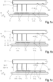
- optoelectronic chips 1 arranged on a wafer with electrical interfaces in the form of contact pads 1.1 and optical interfaces arranged fixedly thereto in the form of optical deflection elements 1.1, e.g. grating couplers or mirrors, are tested with a specific coupling angle ⁇ .
- the specific coupling angle ⁇ represents an angle that an optical signal or its main beam encloses with a perpendicular to the chip 1. It is typically greater than 0° and less than 25°.
- a common value for the specific coupling angle ⁇ is, for example, 11.6° and refers to the glass fibers with the corresponding wedge cut used for coupling in the final application of the chip.
- a wafer is picked up by a positioning table 3 that is adjustable in the x, y and z directions of a Cartesian coordinate system relative to a contacting module 2 and can be rotated about the z axis.
- the contacting module 2 also has optical interfaces 2.2 that can be assigned to them.
- the electrical interfaces and the optical interfaces of the chips 1 are manufactured in the wafer assembly using different technologies and in different process steps, so that although they each have only small positional tolerances among themselves, the electrical interfaces
- the arrangements formed are subject to comparatively large tolerance deviations compared to the arrangements formed by the optical interfaces, particularly with regard to different wafers.
- a first adjustment step the wafer is delivered to the contacting module 2 in such a way that the electrical interfaces in the form of needles 1.1 present on the contacting module 2 are arranged in a first adjustment position (nominal position), perpendicularly above the centers of the contact pads 1.1 of a first of the chips 1.
- the contacting module has an adjustment distance a in the z direction that is greater than the free length l of the needles 2.1 to the chip 1, so that no contact can occur between the needle tips of the needles 2.1 and the contact pads 1.1. See Fig. 1a , whereby for the sake of simplicity, as in the other figures, the representation of the adjustment in the y-direction has been omitted. Accordingly, adjustment paths during individual adjustment steps are only shown as adjustment paths in the x-direction.
- the positional deviation between the arrangements of the electrical interfaces and the arrangements of the optical interfaces of individual chips of a wafer is at least approximately the same.
- the actual position of the optical interfaces of the chip to the optical interfaces on the contacting module 2.2 deviates from a target position due to various reasons, see Fig. 1a .
- the position of the optical interfaces on the chip 1 deviates from their nominal position in the x-, y-, z- and around the z-direction in a statistically variable manner for each wafer, while the deviations around the x- and y-direction can be assumed to be unchangeable due to the alignment of the positioning table 3 after the position of the chip 1 and thus of the wafer has been fixed (systematic deviations).
- the positioning table 3 de facto corrects the position of the entire contacting module 2 to the chip/wafer accordingly - and thus also changes the position of the arrangement of the optical interfaces of the contacting module 2.2 to the arrangement of the optical interfaces on the chip 1 due to the specific coupling angle of the respective optical deflection element, in particular a grating coupler.
- the needles 2.1 as electrical interfaces on the contacting module 2 are optimally aligned with the centers of the contacting pads 1.1 as the electrical interfaces on the chip 1, there is a margin for adjusting the optical interfaces of the chip 1 to those on the contacting module, which is given by the size of the contact pads 1.1, since it is sufficient for the electrical signal conduction that there is mechanical contact between the needle tip and the contact pad.
- a first further adjustment step the relative alignment of the optical interfaces of the chip and the contacting module to each other is carried out by deflecting the positioning table in a scan field smaller than the size of the contact pads, in relation to the first adjustment position in the x and y directions into a second adjustment position (raster scan), as shown in Fig. 1b was represented by the first adjustment path ⁇ x1.
- a second adjustment position raster scan
- an optical signal is passed through at least one of the optical interfaces of the contacting module and the first chip.
- the second adjustment position was taken when the optical signal is coupled in with a maximum intensity. See Fig. 1b .
- the positioning table is deflected in the x and y directions to a third adjustment position, as shown in Fig. 1c by the second Adjustment path ⁇ x2 was shown.
- the adjustment path from the second to the third adjustment position is calculated from the feed path ⁇ z and the coupling angle ⁇ of the relevant grating coupler before the positioning table is fed to the contacting module in the z direction by the feed path ⁇ z to the optical working distance b by pressing the needles against the contact pads with a predetermined constant pressure force. This is achieved by selecting the optical working distance smaller than the free length of the needles l. The difference is referred to as overtravel or overdrive.
- the value of the overtravel must be taken into account in the final adjustment of the chip so that, in the contacted state, it is ensured that an optical working distance is given between the optical interfaces of the contacting module and the chip at which maximum coupling of the optical signals is given.
- the chip is brought into the third adjustment position. In this position, the final adjustment state is created in which both the electrical and the optical interfaces of the chip and the contact module are aligned to each other in the best possible way, i.e. the best possible measurement capability of the optical signal flows is given (maximum position of the optical coupling). where the electrical signal flow is also present.
- electrical or optical signals are then passed through the respective interfaces assigned to each other.
- the adjustment path from the first adjustment position (nominal position) to the third adjustment position (maximum position of the optical coupling) represents an offset (in Fig. 1c , represented as ⁇ x1 + ⁇ x2 , and ⁇ z) which is advantageously stored and taken into account when adjusting all other chips on this wafer.
- This procedure only needs to be performed once per wafer or at even longer intervals.
- the raster scan can also be performed on several chips of the wafer before starting the inspection of all chips of the wafer and the results averaged.
- the required overtravel may change over the lifetime of the contact module due to "running in” or wear of the needles, which reduces the working distance.
- the direct monitoring of the optical working distance is important to ensure the defined optical coupling properties between the contacting module and the chip (measurement capability) and to prevent collisions of the optical interfaces of the contacting module and chips (a few 10-100 ⁇ m distance during operation).
- a distance sensor permanently integrated in the contact module can be used, e.g. a capacitive distance sensor.
- This enables control of the real optical working distance.
- the working distance can be actively adjusted by moving the positioning table in the z-direction and, if necessary, a hard stop can be programmed if the minimum working distance is exceeded, e.g. to avoid a collision due to incorrect operation by the operator.
- a change in the needle tip positions is to be expected when the contact module is first put into operation (run-in behavior). This can be anticipated by multiple contact simulations before adjusting a first chip (pre-aging), which can reduce the value of the offset to be set.
- all optical interfaces of the chips embodied by grating couplers, have coupling angles with the same angular magnitude and the same orientation, so that a change in the optical working distance ⁇ b results in an equal relative change ⁇ X of the optimal coupling position for all optical interfaces.
- the change in the optical working distance ⁇ b is in the range ⁇ 50 ⁇ m. If the optical working distance changes by, for example, 10 ⁇ m and the coupling angle ⁇ is 11.6° in the x-z plane, this would result in a change in the optimal coupling position ⁇ X of 2 ⁇ m in the x-direction. If the optical working distance ⁇ b changes by 20 ⁇ m, this would result in a change in the optimal coupling position ⁇ X of 4 ⁇ m in the x-direction. This can be compensated for by the correction described above, i.e. the positioning table is corrected in the x-direction using a control command, assuming that the needles still hit the contact pads with sufficient reliability.
- the requirements for the accuracy of the adjustment steps can be reduced if the optical signals transmitted for testing the chip via the respective associated interfaces outshine the coupling interface.
- the optical signals exhibit a tophat distribution of their radiation intensity when they impinge on the coupling interface.
Landscapes
- Engineering & Computer Science (AREA)
- Physics & Mathematics (AREA)
- Computer Hardware Design (AREA)
- Microelectronics & Electronic Packaging (AREA)
- General Engineering & Computer Science (AREA)
- General Physics & Mathematics (AREA)
- Health & Medical Sciences (AREA)
- Computer Vision & Pattern Recognition (AREA)
- Electromagnetism (AREA)
- Toxicology (AREA)
- Testing Or Measuring Of Semiconductors Or The Like (AREA)
- Testing Of Individual Semiconductor Devices (AREA)
- Tests Of Electronic Circuits (AREA)
Description
- Die Erfindung betrifft ein Verfahren mit dem in einem Waferprober zeitgleich die Funktionalität von elektrischen und optischen Komponenten bzw. Schaltungen eines Chips auf Wafer - Ebene getestet werden kann. Ein solches Verfahren ist gattungsgemäß aus der
US 2011/0279812 A1 bekannt. - Die Erfindung ist im Bereich des Testens und Qualifizierens von Chips mit optischelektrisch integrierten Schaltungen, sogenannten PICs (Photonic Integrated Circuits), auf Wafer-Ebene angesiedelt. Im Unterschied zu herkömmlichen, rein elektrisch integrierten Schaltungen, sogenannten ICs (Integrated Circuits), sind bei PICs neben den elektrischen Schaltungen auch optische Funktionalitäten integriert.
- Bei der Herstellung von ICs, z. B. mittels CMOS-Technologie, finden in verschiedenen Herstellungsschritten Tests und Messungen statt, um einerseits den Prozess zu überwachen und andererseits eine Qualitätskontrolle durchzuführen. Ein etablierter Test ist dabei der elektrische Wafer Level Test nach der Fertigstellung des Wafers. Hier werden funktionale und nicht-funktionale Chips ermittelt, in einer Wafermap erfasst und damit die Ausbeute bestimmt. Funktionale Chips werden auch als Known Good Dies (KGD) bezeichnet. Beim Vereinzeln des Wafers in einzelne Chips erfolgt dann das Aussortieren der nicht funktionalen Chips. Die für den Wafer Level Test benötigte Testapparatur steht in Form von Waferprobern und Wafertestern mit zugehörigen Kontaktierungsmodulen (auch Probecards genannt) zur Verfügung. Mittels des Kontaktierungsmoduls werden die geräteseitigen Schnittstellen des Wafertesters mit den individuellen Schnittstellen der Chips des auf dem Waferprober fixierten Wafers verbunden. Grundsätzlich kann das Kontaktierungsmodul so ausgeführt sein, dass es nur einen oder aber auch zeitgleich mehrere Chips kontaktiert. Es ist auch nicht zwingend erforderlich, dass die Chips zur Kontaktierung noch im Waferverbund vorliegen. Um gleichzeitig mehrere oder auch nacheinander die Chips eines Wafers zu kontaktieren, müssen die Chips lediglich eine fixierte und definierte Lage zueinander aufweisen.
- Testapparaturen zum Testen rein elektronischer Chips (Halbleiterchip mit ICs) wurden über Jahrzehnte optimiert und diversifiziert, um zur Kostenoptimierung hohe Volumina unterschiedlichster ICs mit hohem Durchsatz qualifizieren zu können.
- Die Herstellung der PICs erfolgt i.d.R. mit den gleichen etablierten Halbleiterprozessen, z. B. der CMOS-Technologie. Die bisher im Vergleich zur IC-Herstellung sehr geringen Fertigungsvolumina von PICs führen dazu, dass i.d.R. in einer Halbleiterfabrik nur Tests zur Prozesscharakterisierung, aber keine funktionalen Tests der PICs durchgeführt werden. Die funktionale Charakterisierung obliegt dem Endkunden und wird oft an gesägten Chips durchgeführt. Die benutzte Testapparatur verwendet voneinander unabhängige, getrennte elektrische und optische Kontaktierungsmodule und ist nicht auf Durchsatz optimiert.
- Das Testen von PICs auf Wafer-Level-Ebene erfordert das Ein- und Auskoppeln von Licht in die bzw. aus der Ebene der PICs, i.d.R. mittels integrierter Grating-Koppler als Koppelstellen, wie in der Fachliteratur "Grating Couplers for Coupling between Optical Fibers and Nanophotonic Waveguides" (D. Taillaert et al, Japanese Journal of Applied Physics, Vol. 45, No. 8A, 2006, S. 6071-6077) beschrieben. Die Gitterkoppler (Grating Couplers) können funktionaler Bestandteil im Chip oder Opferstrukturen auf dem Wafer z. B. im Ritzgraben oder auf benachbarten Chips sein.
- Dem Stand der Technik entsprechend werden glasfaserbasierte Systeme für den Wafer Level Test verwendet, wie in der Fachliteratur: "Test-station for flexible semiautomatic wafer-level silicon photonics testing" beschrieben (J. De Coster et al, 21th IEEE European Test Symposium, ETS 2016, Amsterdam, Netherlands, May 23-27, 2016. IEEE 2016, ISBN 978-1-4673-9659-2). Diese beinhalten ein glasfaserbasiertes Optikmodul, das über einzelne Glasfasern Licht in die Koppelstellen des Chips ein- und auskoppelt. Um eine wiederholgenaue optische Kopplung zu gewährleisten, müssen die Glasfasern zum einen submikrometergenau zu den Koppelstellen in einem Abstand bis zu wenigen Mikrometern justiert werden. Dies ist nur unter Zuhilfenahme hochpräziser Stellelemente möglich, z.B. in Kombination von Hexapoden mit Piezoelementen. Zum anderen muss vor jeder einzelnen optischen Kopplung ein zeitintensiver, aktiver und auf das Erreichen maximaler Koppeleffizienz ausgelegter Justageablauf erfolgen.
- Damit sind bestehende Wafer-Level-Test-Systeme gekennzeichnet durch
- sequentielles, zeitintensives Kontaktieren aller optischen Koppelstellen eines Chips nacheinander, d. h. eine parallele Kontaktierung aller optischen Koppelstellen eines Chips ist nicht oder nur stark eingeschränkt möglich, eine parallele Kontaktierung mehrerer Chips gar nicht möglich.
- geräteseitige Sonderlösungen, so dass herkömmliche Waferprober nur mit aufwendigen und kostenintensiven Modifikationen umrüstbar und danach nicht mehr oder nur bedingt bzw. erst nach zeitaufwendiger Umrüstung für den Wafer Level Test von ICs einsetzbar sind.
- getrennte, nicht fest miteinander verbundene Elektronik- und Optikmodule, d. h. beide müssen separat gehaltert und justiert werden.
- Aus der vorgenannten
US 2006/0109015 A1 ist ein optoelektronisches Kontaktierungsmodul (probe module) zum Testen von Chips (zu untersuchendes Objekt - DUT 140) mit elektrischen und optischen Ein- und Ausgängen bekannt. Das Kontaktierungsmodul stellt eine Schnittstelle zwischen einer Testapparatur (ATE) und dem Testobjekt (device under test, kurz DUT) dar und ist mit elektrischen Kontakten (electical probes), optischen Kontakten (optical probes), optischen Elementen und Kombinationen hiervon ausgeführt, um Signale von dem DUT und zu dem DUT zu leiten und diese Signale umzuverteilen für eine Schnittstelle zur Testapparatur. - Zu den optischen Ein- und Ausgängen ist offenbart, dass diese über optische Elemente geschaffen sind, die sich auf der Kontaktierungsplatte und / oder der Umverteilungsplatte befinden und auf verschiedene Einkoppelmechanismen, z. B. Freistrahlung, Quasifreistrahlung oder Wellenleiter, abgestimmt sind. Als hierfür geeignete optische Elemente sind diffraktive Elemente und refraktive Elemente angegeben. Auch ist angegeben, dass ein Photodetektor oder eine Lichtquelle direkt an der Schnittstelle zum DUT angeordnet sein können, die dann den optischen Ein- oder Ausgang an der Kontaktierungsplatte darstellen.
- Darüber hinaus lehrt die vorgenannte
US 2006/0109015 A1 , dass für Ausführungen der optischen Einkopplung über Freistrahl- oder Quasifreistrahlverbindungen, bei denen das optische Signal durch einen Freiraum zwischen dem optischen Element und der Schnittstelle zum DUT geleitet wird, das optische Signal fokussiert oder kollimiert wird, um eine hohe Einkoppeleffizienz des übertragenen Signals zu erreichen. Die Signaleinkopplung unterliegt hier folglich dem Konzept, das Signal möglichst vollständig einzukoppeln. - Nach einem Ausführungsbeispiel der vorgenannten
US 2006/0109015 A1 sind die optischen und die elektrischen Signalleitungen (optisches und elektrisches Verteilernetz) auf separaten Umverteilungsplatten ausgeführt. Es wird vorgeschlagen, die elektrischen Signale von dem DUT zu den Randbereichen der Kontaktierungsplatte zu führen, so dass in der oberhalb der Kontaktierungsplatte angeordneten ersten Umverteilungsplatte die elektrischen Signale oberhalb des Randbereiches eingekoppelt werden. Dadurch kann in der ersten Umverteilungsplatte, in der nur die elektrischen Signale umverteilt werden, eine Öffnung ausgebildet sein, durch die hindurch die optischen Signale in eine darüber angeordnete separate zweite Umverteilungsplatte geführt werden. - Zusammenfassend werden in der vorgenannten
US 2006/0109015 A1 eine Vielzahl von Ideen aufgezeigt, wie ein Kontaktierungsmodul, das begründet, z. B. durch den Verschleiß der mechanischen Kontakte für die elektrische Signalübertragung, in eine Kontaktierungsplatte und eine Umverteilungsplatte unterteilt ist, zusätzlich mit optischen Signalleitungen ausgestattet werden könnte. Dabei wird völlig außer Betracht gelassen, dass die für den mechanischen Kontakt der elektrischen Ein- und Ausgänge des Kontaktierungsmoduls zum DUT möglichen Toleranzen nicht auf die optischen Ein- und Ausgänge übertragbar sind. - Während die Übertragung eines stets gleichen elektrischen Signals lediglich einen mechanischen Kontakt von an dem Kontaktierungsmodul vorhandenen Nadeln mit an dem DUT vorhandenen Kontaktplättchen (Kontaktpads) erfordert, was innerhalb einer vergleichsweise großen Lagetoleranz von einigen µm in alle drei Raumrichtungen gesichert werden kann, wird die Qualität der optischen Signalübertragung bereits bei einer sehr viel kleineren, im Sub-µm-Bereich liegenden Abweichung von einer Solllage beeinflusst.
- Erfolgt, wie in der vorgenannten
US 2006/0109015 A1 beschrieben, eine Optimierung der Koppeleffizienz des optischen Signals durch eine Kollimation oder Fokussierung des optischen Strahls, muss das gesamte Kontaktierungsmodul hochpräzise im Sub-µm-Bereich justiert werden. Andernfalls ist die justageabhängige Wiederholgenauigkeit der Messung nicht ausreichend für die beschriebenen Anwendungen. Das wiederum hat zur Folge, dass das Kontaktierungsmodul nicht die in herkömmlichen elektrischen Waferprobern typischen Justagetoleranzen für die elektrische Kontaktierung im Bereich von einigen Mikrometern in X-, Y- und Z-Richtung ausschöpfen kann. Es werden aufwendige und teure Waferprober-Sonderlösungen u. a. mit diversen Stellelementen, wie zum Beispiel Piezostellelementen, und Linearachsen oder Hexapoden benötigt, um das Kontaktierungsmodul hochgenau zum DUT zu justieren. - Ein weiterer kritischer Punkt ist, dass für die saubere elektrische Justage der Nadeln ein sogenannter Overdrive von typisch einigen 10 µm in Z-Richtung eingestellt wird, d. h. dass nach Erstkontakt der Nadeln mit den elektrischen Kontaktpads das Kontaktierungsmodul noch um einen zusätzlichen Betrag in Z-Richtung verfahren wird, um eine zuverlässige elektrische Kontaktierung zu gewährleisten. Abnutzung und Verformung der Nadeln werden i.d.R. durch eine Anpassung des Overdrives während des Betriebes gegenkompensiert. Bei einer einfachen Kollimation oder Fokussierung des optischen Strahls, wie in der vorgenannten
US 2006/0109015 A1 beschrieben, darf für eine wiederholgenaue Kopplung der Arbeitsabstand in Z-Richtung jedoch nur im Bereich um Mikrometer schwanken. Damit ist diese Art der optischen Kopplung nicht kompatibel mit etablierten elektrischen Kontaktierungsverfahren. - Die
US 2011/0279812 A1 offenbart ein Kontaktierungsmodul zum Testen von Chips mit elektrischen und optischen Ein- und Ausgängen. Der Chip ist auf einem beweglichen Träger aufgenommen, mit dem er sich grob zum Kontaktierungsmodul ausrichten lässt. Die Grobausrichtung erfolgt sensorgesteuert anhand einer Positionsüberwachung des Chips oder der Justiermarken des Chips. Die Feinausrichtung des Chips erfolgt in zwei Verfahrensschritten. Im ersten Verfahrensschritt wird überprüft, ob die elektrischen Ein- und Ausgänge in Kontakt zum Kontaktierungsmodul stehen. Der Chip wird dazu mit dem Kontaktierungsmodul angesaugt, sodass die elektrischen Ein- und Ausgänge des Chips mit den elektrischen Kontakten des Kontaktierungsmoduls in Kontakt kommen. Mittels eines Testsignals wird auf eine erfolgreiche Kontaktierung geprüft und bei fehlerhafter Kontaktierung mittels einer wiederholten Grobausrichtung korrigiert. Im zweiten Verfahrensschritt erfolgt die Ausrichtung an den optischen Ein- und Ausgängen. Die optischen Ein- und Ausgänge des Chips können fokussierte oder kollimierte Strahlen mit angepasster Apertur und Fokusposition empfangen oder aussenden. Die optischen Ein- und Ausgänge des Kontaktierungsmoduls verfügen über variable Optiken, mit denen senkrecht auf die Oberfläche der optischen Ein- und Ausgänge fokussierte Strahlen erzeugt werden können, wobei die axiale und seitliche Fokuslage und die Apertur der Strahlen anpassbar sind. Für die Anpassung verfügt die variable Optik über mindestens ein optisches Element mit veränderbarer Brennweite und/oder mindestens ein optisches Element, das beweglich ist. Die axiale Anpassung der Fokuslage erfolgt auf Grundlage von Abstandsmessungen mittels zusätzlicher Abstandssensoren oder von Intensitätsmessungen anhand eines optischen Testsignals. Die seitliche Anpassung der Fokuslage erfolgt auf Grundlage von Intensitätsmessungen, bei denen ein bereits auf die Oberfläche des Chips fokussierter Teststrahl in einer scannenden Relativbewegung gegenüber den optischen Ein- und Ausgängen bewegt wird, bis der Teststrahl optimal in die optischen Ein- und Ausgänge eingekoppelt wird. Die dafür benötigte Zeit kann verkürzt werden, indem die scannende Relativbewegung zunächst mit einem vergrößerten Fokusdurchmesser des Teststrahls ausgeführt wird. Nach der Feinausrichtung erfolgt der Test des Chips mittels spezieller elektrischer und optischer Testsignalsequenzen, wobei beim Testen mehrerer gleichartiger Chips Teile der Grob- und Feinjustage abgespeichert und weiter verwendet werden können. - Zum Testen von elektronischen Chips auf Waferebene ist es aus der Praxis bekannt, dass mittels einer ersten Kamera die Raumlage der Spitzen der Nadeln und mit einer zweiten Kamera die Raumlage der Mittelpunkte der Kontaktpads eines Chips bestimmt werden. Aus einer daraus abgeleiteten Relativlage der Spitzen zu den Kontaktpads werden Steuersignale gebildet, mit denen ein Positioniertisch angesteuert wird und die Mittelpunkte der Kontaktpads lotrecht unterhalb der Spitzen positioniert werden, bevor die Kontaktnadeln mit den Kontaktpads in Kontakt gebracht werden. Ein weiteres Verfahren zum Testen von auf einem Wafer angeordneten opto-elektrischen Chips ist in
WO 2019/029765 A beschrieben. - Es ist die Aufgabe der Erfindung ein Verfahren zum Testen von auf einem Wafer angeordneten optoelektronischen Chips mit elektrischen Schnittstellen in Form von Kontaktpads und hierzu fest angeordneten optischen Schnittstellen in Form von optischen Umlenkelementen mit einem spezifischen Kopplungswinkel zu finden, das auf bewährten Verfahren zum Testen von elektronischen Chips basiert.
- Diese Aufgabe wird mit einem Verfahren zum Testen von auf einem Wafer angeordneten opto-elektronischen Chips mit elektrischen Schnittstellen in Form von Kontaktpads und hierzu fest angeordneten optischen Schnittstellen in Form von optischen Umlenkelementen gelöst. Die optischen Umlenkelemente weisen einen spezifischen Kopplungswinkel auf.
- Dabei wird der Wafer von einem in x -, y- und z- Richtung eines kartesischen Koordinatensystems verstellbaren und um die z Achse drehbaren Positioniertisch aufgenommen. Es ist ein Kontaktierungsmodul vorhanden, welches über zu den Chips zugeordnete elektrische Schnittstellen und optische Schnittstellen verfügt und gegenüber dem Positioniertisch verstell- und verdrehbar ist.
- In einem ersten Justierschritt wird der Wafer dem Kontaktierungsmodul so zugestellt, dass die an dem Kontaktierungsmodul vorhandenen elektrischen Schnittstellen in Form von Nadeln, in einer ersten Justierlage, lotrecht oberhalb der Mittelpunkte der Kontaktpads eines ersten der Chips angeordnet sind. In dieser ersten Justierlage ist das Kontaktierungsmodul in z-Richtung in einem Justierabstand größer einer freien Länge der Nadeln zu dem ersten der Chips angeordnet, sodass die Nadeln während der nächsten Justierschritte keinen Kontakt zu den Kontaktpads haben
- Aus dieser ersten Justierlage heraus erfolgt in weiteren Justierschritten die relative Ausrichtung der optischen Umlenkelemente zu den an dem Kontaktierungsmodul vorhandenen optischen Schnittstellen. Die Kontaktpads sind so dimensioniert, dass die bei den weiteren Justierschritten erforderlichen Stellwege nur so groß sind, dass die Nadel nach einem abschließenden Absenken Kontakt mit den Kontaktpads erlangen.
- Es wird in einem Scanfeld kleiner der Größe der Kontaktpads zuerst der Positioniertisch gegenüber der ersten Justierlage in x- und y-Richtung in eine zweite Justierlage ausgelenkt. Währenddessen wird über wenigstens eine der optischen Schnittstellen des Kontaktierungsmoduls und eines der optischen Umlenkelemente ein optisches Signal geleitet wird. Die zweite Justierlage ist dann eingenommen, wenn das optische Signal mit einer maximalen Intensität eingekoppelt wird. Anschließend wird der erste der Chips über einen Stellweg in eine dritte Justierlage in x-y- Richtung ausgelenkt wird, nachdem der Stellweg aus dem Zustellweg und dem Kopplungswinkel des betreffenden optischen Umlenkelementes berechnet wurde.
- Anschließend wird der Positioniertisch dem Kontaktierungsmodul in z-Richtung um einen Zustellweg in einen optischen Arbeitsabstand zugestellt, indem die Nadeln mit einer vorgegebenen Andruckkraft an den Kontaktpads anliegen.
- Zum Testen des opto-elektronischen Chips werden jetzt über die jeweils einander zugeordneten Schnittstellen elektrische bzw. optische Signale geleitet Vorteilhaft wird eine sich aus der ersten Justierlage und der zweiten Justierlage des ersten der Chips ergebende Lagedifferenz als Offset abgespeichert und für die Justierung weiterer der Chips berücksichtigt, nachdem diese in einer ersten Justierlage zum Kontaktierungsmodul positioniert wurden.
- Insbesondere um den Verschleiß der Nadelspitzen zu berücksichtigen, ist es von Vorteil, wenn der optische Arbeitsabstand, bei dem die Nadeln mit einer vorgegebenen Andruckkraft an den Kontaktpads anliegen, überwacht wird und bei Änderungen der Andruckkraft die dritte Justierlage korrigiert wird.
- Indem die Änderung des optischen Arbeitsabstandes langfristig über die Einsatzdauer des Kontaktierungsmoduls ermittelt wird, ist es vorteilhaft möglich für die Verfahrensdurchführung die Nadeln des Kontaktierungsmoduls gegen neue Nadeln zu ersetzen, wenn der optische Arbeitsabstand einen vorgegebenen Minimalabstand unterschreitet.
- Indem die optischen Signale die jeweilige Schnittstelle beim Einkoppeln vorteilhaft überstrahlen, werden insbesondere Lagetoleranzen der optischen Schnittstellen der Chips untereinander ausgeglichen.
- Noch vorteilhafter ist es, wenn die über die jeweils einander zugeordneten Schnittstellen geleiteten optische Signale beim Einkoppeln eine Tophat-Verteilung ihrer Strahlungsintensität aufweisen.
- Die Erfindung soll nachfolgend anhand von Ausführungsbeispielen unter Zuhilfenahme von Zeichnungen näher erläutert werden. Hierzu zeigt:
- Fig. 1a
- einen Chip in einer ersten Justierlage (Nominalposition) zum Kontaktierungsmodul angeordnet,
- Fig. 1b
- der Chip in einer zweiten Justierlage zum Kontaktierungsmodul angeordnet und
- Fig. 1c
- der Chip in einer dritten Justierlage (Maximum-Position der optischen Kopplung) zum Kontaktierungsmodul angeordnet.
- Mit einem erfindungsgemäßen Verfahren werden von auf einem Wafer angeordnete opto-elektronische Chips 1 mit elektrischen Schnittstellen in Form von Kontaktpads 1.1 und hierzu fest angeordnete optische Schnittstellen in Form von optischen Umlenkelementen 1.1, z.B. Gitterkopplern oder Spiegeln, mit einem spezifischen Kopplungswinkel α getestet. Der spezifische Kopplungswinkel α stellt einen Winkel dar, den ein optisches Signal bzw. dessen Hauptstrahl mit einem Lot auf den Chip 1 einschließt. Er ist typischerweise größer 0° und kleiner 25°. Ein gängiger Wert für den spezifischen Koppelungswinkel α liegt z.B. bei 11,6° und bezieht sich auf die zur Kopplung in der Endanwendung des Chips verwendeten Glasfasern mit entsprechendem Keilanschliff.
- Dabei wird gleich einem Verfahren des Standes der Technik ein Wafer von einem in x -, y - und z- Richtung eines kartesischen Koordinatensystems gegenüber einem Kontaktierungsmodul 2, verstellbaren und um die z Achse drehbaren Positioniertisch 3 aufgenommen. Das Kontaktierungsmodul 2 verfügt neben über zu den Chips 1 zuordenbaren elektrische Schnittstellen 2.1 auch über hierzu zuordenbaren optische Schnittstellen 2.2. Die elektrischen Schnittstellen und die optischen Schnittstellen der Chips 1 werden im Waferverbund mit unterschiedlichen Technologien und in unterschiedlichen Verfahrensschritten hergestellt, so dass sie jeweils untereinander zwar nur geringe Lagetoleranzen aufweisen, die durch die elektrischen Schnittstellen gebildete Anordnungen unterliegen jedoch gegenüber den durch die optischen Schnittstellen gebildete Anordnungen insbesondere bezogen auf verschiedene Wafer vergleichsweise großen Toleranzabweichungen.
- In einem ersten Justierschritt, wird der Wafer dem Kontaktierungsmodul 2 so zugestellt, dass die an dem Kontaktierungsmodul 2 vorhandenen elektrischen Schnittstellen in Form von Nadeln 1.1, in eine erste Justierlage (Nominalposition), lotrecht oberhalb der Mittelpunkte der Kontaktpads 1.1 eines ersten der Chips 1 angeordnet werden. Während der Justierung weist der Kontaktierungsmodul in z-Richtung einen Justierabstand a auf, größer der freien Länge l der Nadeln 2.1 zu dem Chip 1, sodass es zu keinem Kontakt zwischen den Nadelspitzen der Nadeln 2.1 und den Kontaktpads 1.1 kommen kann. Siehe hierzu
Fig. 1a , wobei hier der Einfachheit halber, wie auch in den andren Figuren, auf die die Darstellung der Justierung in y-Richtung verzichtet wurde. Entsprechend sind Stellwege während einzelner Justierschritte nur als Stellwege in x-Richtung dargestellt. - Der Ablauf dieses ersten Justierschrittes erfolgt vorteilhaft gemäß einer aus der Praxis bekannten festen Routine. Dabei misst eine Kamera die Nadeln 2, durch Fokussierung auf die Nadelspitzen, und eine zweite Kamera misst die Kontaktpads 1.1 des Chips 1 ein. Beide Kameras sind vorher über ein Normal zueinander referenziert worden. Das ermöglicht anschließend die genaue Berechnung der optimalen Position (Nominalposition) der Nadeln 2 in Bezug auf die Kontaktpads 1.1 und damit die Positionierung des Kontaktmoduls 2 zum Chip 1. Meistens geschieht das über Regression und Extrapolation der Messwerte. Zudem wird zu jeder gefundenen Nadel 2 auch ein Kontaktpad 1.1 als Gegenstück erwartet. In diese Routine kann durch den Nutzer im Regelfall nicht eingegriffen werden. Auch können meist keine alternativen Strukturen wie Justiermarken etc. für die Positionierung verwendet werden. Über die Kameras wird nicht nur die x-y Position sowie eine Verdrehung um die z-Achse korrigiert, sondern auch die z-Position ermittelt.
- Es ist dem Fachmann klar, dass aufgrund von Lagetoleranzen der Nadelspitzen zueinander und der Mittelpunkte der Kontaktpads 1.1 zueinander zeitgleich nicht wirklich alle Nadelspitzen exakt oberhalb der Mittelpunkte der Kontaktpads 1.1 angeordnet werden können und man letztendlich eine Position einjustiert in der die mittlere Abweichung am geringsten ist. Die Lagetoleranz der elektrischen Schnittstellen zueinander, ist jedoch vernachlässigbar klein im Vergleich zu der Lagetoleranz der Anordnung der elektrischen Schnittstellen zu der Anordnung der optischen Schnittstellen eines Chips 1, was seine Ursache insbesondere darin hat, dass die elektrischen Schnittstellen und die optischen Schnittstellen nacheinander mit unterschiedlichen Technologien hergestellt werden.
- Da die Herstellung der elektrischen Schnittstellen bzw. die Herstellung der optischen Schnittstellen für alle Chips eines Wafers jeweils in einem Verfahrensablauf erfolgt ist die Lageabweichung zwischen den Anordnungen der elektrischen Schnittstellen und den Anordnungen der optischen Schnittstellen einzelner Chips eines Wafers wenigstens annähernd gleich.
- Nachdem die Anordnung der elektrischen Kontakte des Chips 1 (Nadeln 2.1) zu den elektrischen Kontakten des Kontaktierungsmodul 2 (Kontaktpads 1) ausgerichtet ist, weicht die tatsächliche Position der optischen Schnittstellen des Chips zu den optischen Schnittstellen am Kontaktierungsmodul 2.2 aufgrund verschiedener Ursachen von einer Solllage ab, siehe
Fig. 1a . - So weicht erstens die Lage der optischen Schnittstellen am Chip 1 von ihrer Sollposition in x-, y-, z- und um die z-Richtung statistisch veränderlich bei jedem Wafer ab, während die Abweichungen um die x- und um die y-Richtung durch die Ausrichtung des Positioniertisches 3 nach erfolgter Lagefixierung des Chips 1 und damit des Wafers als unveränderlich angenommen werden können (systematische Abweichungen).
- Zweitens gibt es eine Abweichung der Lage der optischen Schnittstellen am Kontaktierungsmodul 2.2 von einer Solllage in Bezug zu den Nadeln 2.1, abhängig von der Montagegenauigkeit des optischen Moduls, welches integraler Bestandteil des Kontaktierungsmoduls ist. Dies betrifft nicht nur Lageabweichungen in x-, y- und z-Richtung, sondern auch Verkippungen um die z-, sowie um die x- und um die y-Richtung. Es handelt sich bei allen 6 Parametern um montagebedingte, systematische Abweichungen.
- Und drittens kommt es über die Lebensdauer des Kontaktierungsmoduls 2 zu veränderlichen Abweichungen. Der Grund dafür ist die mechanische Abnutzung und damit Formänderung der Nadelspitzen sowie mögliche Verbiegungen und der daraus resultierenden Änderung im Fitergebnis.
- Über die Kameramessung korrigiert der Positioniertisch 3 de facto die Position des gesamten Kontaktierungsmoduls 2 zum Chip/Wafer entsprechend nach - und ändert damit auch aufgrund des spezifischen Kopplungswinkels des jeweiligen optischen Umlenkelementes, insbesondere eines Gitterkopplers, die Position der Anordnung der optischen Schnittstellen des Kontaktierungsmoduls 2.2 zu der Anordnung der optischen Schnittstellen am Chip 1.
- In weiteren Justierschritten erfolgt jetzt die relative Ausrichtung der optischen Schnittstellen des ersten Chips 1 zu den an dem Kontaktierungsmodul vorhanden optischen Schnittstellen
- Davon ausgehend, dass die Nadeln 2.1 als elektrische Schnittstellen am Kontaktierungsmodul 2 optimal zu den Mittelpunkten der Kontaktierungspads 1.1 als den elektrischen Schnittstellen am Chip 1 ausgerichtet sind, ist für die Justierung der optischen Schnittstellen des Chips 1 zu denen am Kontaktierungsmodul ein Spielraum gegeben, der durch die Größe der Kontaktpads 1.1 gegeben ist, da es für die elektrische Signalleitung ausreichend ist, dass ein mechanischer Kontakt zwischen der Nadelspitze und dem Kontaktpad besteht.
- In einem ersten weiteren Justierschritt erfolgt die relative Ausrichtung der optischen Schnittstellen von Chip und Kontaktierungsmodul zueinander, indem in einem Scanfeld kleiner der Größe der Kontaktpads der Positioniertisch, gegenüber der ersten Justierlage in x- und y-Richtung in eine zweite Justierlage ausgelenkt wird (Rasterscan), wie in
Fig. 1b durch den ersten Stellweg Δx1 dargestellt wurde. Während dessen wird über wenigstens eine der optischen Schnittstellen des Kontaktierungsmoduls und des ersten Chips ein optisches Signal geleitet. Die zweite Justierlage wurde eingenommen, wenn das optische Signal mit einer maximalen Intensität eingekoppelt wird. Siehe hierzuFig. 1b . - Anschließend wird der Positioniertisch in einem zweiten weiteren Justierschritt in x- und y- Richtung in eine dritte Justierlage ausgelenkt, wie in
Fig. 1c durch den zweiten Stellweg Δx2 dargestellt wurde. Der Justierweg von der zweiten in die dritte Justierlage wird aus dem Zustellweg Δz und dem Kopplungswinkel α des betreffenden Gitterkopplers berechnet, bevor der Positioniertisch dem Kontaktierungsmodul in z-Richtung um den Zustellweg Δz in den optischen Arbeitsabstand b zugestellt wird, indem die Nadeln mit einer vorgegebenen konstanten Andruckkraft an den Kontaktpads anliegen. Das wird erreicht in dem der optische Arbeitsabstand kleiner der freien Länge der Nadeln l gewählt wird. Die Differenz wird als Overtravel oder auch Overdrive bezeichnet. - Mit dem Overtravel wird ein sicherer elektrischer Kontakt der Nadeln mit den Kontaktpads gewährleistet (geringer Kontaktwiderstand). Nach dem ersten leichten Kontakt der Nadeln mit den Kontaktpads wird der Wafer noch um einige 10µm in z-Richtung nach oben gefahren. Damit werden zwei Sachen erreicht. Einerseits wird damit ein Scratchen der Nadeln über das Kontaktpad forciert, wodurch die Oxidoberfläche durchbrochen und ein reproduzierbarer, niederohmiger Kontakt erreicht wird. Andererseits wird durch den Overtravel ein konstanter Anpressdruck der Nadeln erzeugt, da die Nadeln aufgrund des zusätzlichen Stellweges entsprechend einfedern und eine Andruckkraft auf das Kontaktpad ausüben. Diese Andruckkraft ist je nach verwendetem Nadeltyp unterschiedlich, man kann aber größenordnungsmäßig von ca. 3g pro Nadel ausgehen. Typischerweise wird der Overtravel in Vielfachen von MIL angegeben (amerik. 1mil = 1/1000 Zoll = 0,0254mm)
- Bei einem Kontaktierungsmodul, bei dem die Anordnung der Nadel eine feste Lage zu den optischen Schnittstellen aufweist, muss der Wert des Overtravels bei der finalen Justierung des Chips berücksichtigt werden, sodass im kontaktierten Zustand sichergestellt wird, dass ein optischer Arbeitsabstand zwischen den optischen Schnittstellen des Kontaktierungsmoduls und dem Chip gegeben ist, beim dem eine maximale Einkopplung der optischen Signale gegeben ist.
- Um den optischen Arbeitsabstand b einzustellen wird der Chip in die dritte Justierlage gebracht. In dieser ist der finale Justierzustand hergestellt, in dem sowohl die elektrischen als auch die optischen Schnittstellen von Chip und Kontaktierungsmodul bestmöglich zueinander ausgerichtet sind, das heißt eine bestmögliche Messfähigkeit der optischen Signalflüsse gegeben ist (Maximum-Position der optischen Kopplung), wobei auch der elektrische Signalfluss gegeben ist. Zur Prüfung des Chips werden anschließend über die jeweils einander zugeordneten Schnittstellen elektrische bzw. optische Signale geleitet.
- Der Justierweg von der ersten Justierlage (Nominalposition) in die dritte Justierlage ((Maximum-Position der optischen Kopplung) stellt einen Versatz (Offset) dar (in
Fig. 1c , als Δx1 +Δx2 , und Δz dargestellt) der vorteilhaft gespeichert wird und bei der Einjustierung aller weiteren Chips auf diesem Wafer mitberücksichtigt wird. D.h. die Nominalposition des Positioniertisches wird um diesen Versatz korrigiert. Das setzt jedoch eine entsprechend Verschiebung der Nadeln über den Kontaktpads voraus, die noch tolerierbar ist. - Diese Prozedur muss nur einmal pro Wafer oder auch in noch größeren Abständen durchgeführt werden.
- Zudem kann dieser Versatzwert (Offset-Wert) und seine Änderungen über die Zeit beobachtet werden und lässt damit Aussagen über die Abnutzung und damit verbundene Veränderung der Nadeln zu.
- Zu Erhöhung der Genauigkeit der Bestimmung des Versatzes kann der Rasterscan auch an mehreren Chips des Wafers vor Beginn der Prüfung aller Chips des Wafers durchgeführt und die Ergebnisse gemittelt werden.
- Der benötigte Overtravel kann sich über die Lebensdauer des Kontaktierungsmoduls aufgrund eines "Einlaufens" oder durch Abnutzung der Nadeln ändern, womit sind der Arbeitsabstand verringert.
- Die direkte Überwachung des optischen Arbeitsabstandes ist wichtig, um die definierten optischen Kopplungseigenschaften zwischen dem Kontaktierungsmodul und dem Chip zu gewährleisten (Messfähigkeit) und Kollisionen der optischen Schnittstellen von Kontaktierungsmodul und Chips zu verhindern (wenige 10-100µm Abstand im Betrieb).
- Dafür kann ein fest im Kontaktierungsmodul integrierter Abstandssensor verwendet werden, z.B. ein kapazitiver Abstandssensor. Dieser ermöglicht eine Kontrolle des realen optischen Arbeitsabstandes. In Kombination mit einer aktiven Regelung kann der Arbeitsabstand durch Verfahren des Positioniertisches in z-Richtung aktiv nachgeregelt werden und bei Bedarf ein Hard Stop für die Unterschreitung eines Mindestarbeitsabstandes einprogrammiert werden, z.B. um eine Kollision durch Fehlbedienung des Operators zu vermeiden.
- Typischerweise ist eine Veränderung der Nadelspitzenpositionen bei der Erstinbetriebnahme des Kontaktierungsmoduls zu erwarten (Einlaufverhalten). Dies kann durch eine mehrfache Kontaktsimulation vor der Einjustierung eines ersten Chips vorweggenommen werden (Voraltern), womit der Wert des einzustellenden Versatzes reduziert werden kann.
- Üblicherweise weisen alle optischen Schnittstellen der Chips, verkörpert durch Gitterkoppler, Kopplungswinkel mit einem gleichen Winkelbetrag und einer gleichen Ausrichtung auf, so dass sich aus einer Änderung des optischen Arbeitsabstandes Δb entsprechend eine gleiche relative Änderung ΔX der optimalen Koppelposition für alle optischen Schnittstellen ergibt.
- Typischerweise liegt die Änderung des optischen Arbeitsabstandes Δb im Bereich <50µm. Bei einer Änderung des optischen Arbeitsabstandes von beispielsweise 10µm und einem Kopplungswinkel α von 11.6° in der x-z-Ebene ergäbe sich damit in x-Richtung eine Änderung der optimalen Koppelposition ΔX von 2µm. Bei einer Änderung des optischen Arbeitsabstandes Δb von 20µm ergäbe sich in x-Richtung eine Änderung der optimalen Koppelposition ein ΔX von 4µm. Dies kann durch die oben beschriebene Korrektur noch abgefangen werden, d.h. der Positioniertisch wird in x-Richtung per Steuerbefehl unter der Annahme nachkorrigiert, dass die Nadeln immer noch ausreichend sicher auf die Kontaktpads treffen.
- Die Anforderungen an die Genauigkeit der Justierschritte kann reduziert werden, wenn die zur Prüfung des Chips über die jeweils einander zugeordneten Schnittstellen geleiteten optische Signale die einkoppelnde Schnittstelle jeweils überstrahlen.
- Vorteilhaft weisen die optischen Signale beim Auftreffen auf die einkoppelnde Schnittstelle eine Tophat-Verteilung ihrer Strahlungsintensität auf.
-
- 1
- Chip
- 1.1
- Kontaktpad
- 1.2
- optisches Umlenkelement
- 2
- Kontaktierungsmodul
- 2.1
- Nadel
- 2.2
- optische Schnittstelle am Kontaktierungsmodul
- 3
- Positioniertisch
- Δz
- Zustellweg
- α
- Kopplungswinkel
- a
- Justierabstand
- b
- optischer Arbeitsabstand
- l
- freie Länge der Nadel
- Δx1
- erster Stellweg
- Δx2
- zweiter Stellweg
Claims (6)
- Verfahren zum Testen von auf einem Wafer angeordneten opto-elektronischen Chips (1), mit elektrischen Schnittstellen in Form von Kontaktpads (1.1) und hierzu fest angeordneten optischen Schnittstellen in Form von optischen Umlenkelementen (1.2), mit einem spezifischen Kopplungswinkel (α),bei dem der Wafer von einem Positioniertisch (3) aufgenommen wird, der in x -, y- und z- Richtung eines kartesischen Koordinatensystems gegenüber einem Kontaktierungsmodul (2) verstellbar und um die z-Achse drehbar ist, wobei das Kontaktierungsmodul (2) den Kontaktpads (1.1) zugeordnete elektrische Schnittstellen in Form von Nadeln (2.1) und den optischen Umlenkelementen (1.2) zugeordnete optische Schnittstellen (2.2) aufweist, undin einem ersten Justierschritt der Wafer dem Kontaktierungsmodul (2) so zugestellt wird, dass die Nadeln (2.1), in einer ersten Justierlage, lotrecht oberhalb der Mittelpunkte der Kontaktpads (1.1) eines ersten der Chips (1) angeordnet sind, wobei das Kontaktierungsmodul (2) in z-Richtung einen Justierabstand (a) größer einer freien Länge (I) der Nadeln (2.1) zu dem ersten der Chips (1) aufweist,in weiteren Justierschritten die relative Ausrichtung der optischen Umlenkelemente (1.2) zu den an dem Kontaktierungsmodul (2) vorhandenen optischen Schnittstellen (2.2) erfolgt,dann der Positioniertisch (3) dem Kontaktierungsmodul (2) in z-Richtung um einen Zustellweg (Δz) in einen optischen Arbeitsabstand (b) zugestellt wird, bei dem die Nadeln (2.1) mit einer vorgegebenen Andruckkraft an den Kontaktpads (1.1) anliegen, undanschließend über die jeweils einander zugeordneten Schnittstellen elektrische bzw. optische Signale geleitet werden, dadurch gekennzeichnet,dass die relative Ausrichtung der optischen Umlenkelemente (1.2) zu den an dem Kontaktierungsmodul (2) vorhandenen optischen Schnittstellen (2.2) erfolgt, indem in einem Scanfeld kleiner der Größe der Kontaktpads (1.1) zuerst der Positioniertisch (3) gegenüber der ersten Justierlage in x- und y-Richtung in eine zweite Justierlage ausgelenkt wird, während über wenigstens eine der optischen Schnittstellen des Kontaktierungsmoduls (2.2) und eine der optischen Umlenkelemente (1.2) ein optisches Signal geleitet wird, wobei die zweite Justierlage eingenommen ist, wenn das optische Signal mit einer maximalen Intensität eingekoppelt wird, undanschließend der erste der Chips (1) über einen Stellweg in eine dritte Justierlage in x-y- Richtung ausgelenkt wird, wobei der Stellweg aus dem Zustellweg (Δz) und dem Kopplungswinkel (α) des betreffenden optischen Umlenkelementes (1.2) berechnet wurde, bevor der Positioniertisch (3) dem Kontaktierungsmodul (2) in z-Richtung um den Zustellweg (Δz) in den optischen Arbeitsabstand (b) zugestellt wird.
- Verfahren zum Testen von auf einem Wafer angeordneten opto-elektronischen Chips (1) nach Anspruch 1, dadurch gekennzeichnet,
dass eine sich aus der ersten Justierlage und der zweiten Justierlage des ersten der Chips (1) ergebende Lagedifferenz als Offset abgespeichert wird und für die Justierung weiterer der Chips (1) berücksichtigt wird, nachdem diese in einer ersten Justierlage zum Kontaktierungsmodul (2) positioniert wurden. - Verfahren zum Testen von auf einem Wafer angeordneten opto-elektronischen Chips (1) nach Anspruch 1 oder 2, dadurch gekennzeichnet,
dass der optische Arbeitsabstand (b), bei dem die Nadeln (2.1) mit einer vorgegebenen Andruckkraft an den Kontaktpads (1.1) anliegen, überwacht wird und bei Änderungen der Andruckkraft die dritte Justierlage korrigiert wird. - Verfahren zum Testen von auf einem Wafer angeordneten opto-elektronischen Chips (1) nach einem der Ansprüche 1 bis 3, dadurch gekennzeichnet,
dass die Änderung des optischen Arbeitsabstandes (b) langfristig über die Einsatzdauer des Kontaktierungsmoduls (2) ermittelt wird und für die Verfahrensdurchführung die Nadeln (2.1) des Kontaktierungsmoduls (2) gegen neue Nadeln (2.1) ersetzt werden, wenn der optische Arbeitsabstand (b) einen vorgegebenen Minimalabstand unterschreitet. - Verfahren zum Testen von auf einem Wafer angeordneten opto-elektronischen Chips (1) nach einem der Ansprüche 1 oder 2, dadurch gekennzeichnet,
dass die über die jeweils einander zugeordneten Schnittstellen geleiteten optischen Signale beim Einkoppeln in einer der Schnittstellen diese überstrahlen. - Verfahren zum Testen von auf einem Wafer angeordneten opto-elektronischen Chips (1) nach einem der Ansprüche 1 oder 2, dadurch gekennzeichnet,
dass die über die jeweils einander zugeordneten Schnittstellen geleiteten optischen Signale beim Einkoppeln in eine der Schnittstellen eine Tophat-Verteilung ihrer Strahlungsintensität aufweisen.
Applications Claiming Priority (2)
| Application Number | Priority Date | Filing Date | Title |
|---|---|---|---|
| DE102019007516 | 2019-10-25 | ||
| PCT/DE2020/100521 WO2021078318A1 (de) | 2019-10-25 | 2020-06-19 | Wafer-level-testverfahren für opto-elektronische chips |
Publications (2)
| Publication Number | Publication Date |
|---|---|
| EP4049048A1 EP4049048A1 (de) | 2022-08-31 |
| EP4049048B1 true EP4049048B1 (de) | 2025-02-12 |
Family
ID=71614659
Family Applications (1)
| Application Number | Title | Priority Date | Filing Date |
|---|---|---|---|
| EP20740227.2A Active EP4049048B1 (de) | 2019-10-25 | 2020-06-19 | Wafer-level-testverfahren für opto-elektronische chips |
Country Status (6)
| Country | Link |
|---|---|
| US (1) | US11906579B2 (de) |
| EP (1) | EP4049048B1 (de) |
| JP (1) | JP7509199B2 (de) |
| ES (1) | ES3026766T3 (de) |
| FI (1) | FI4049048T3 (de) |
| WO (1) | WO2021078318A1 (de) |
Families Citing this family (6)
| Publication number | Priority date | Publication date | Assignee | Title |
|---|---|---|---|---|
| DE102021110102B4 (de) | 2021-04-16 | 2024-05-23 | Jenoptik Optical Systems Gmbh | Wafer-Level-Testverfahren für opto-elektronische Chips |
| US12210057B2 (en) | 2021-04-16 | 2025-01-28 | Jenoptik Optical Systems Gmbh | Wafer-level test method for optoelectronic chips |
| DE102023120242A1 (de) | 2023-07-31 | 2025-02-06 | Jenoptik Optical Systems Gmbh | Prüfanordnung zum Prüfen von optischen Komponenten, Verfahren zum Betreiben einer Prüfanordnung sowie Steuereinheit |
| DE102024119860B3 (de) | 2024-07-12 | 2025-08-21 | Jenoptik Optical Systems Gmbh | Optisches Koppelmodul zum Testen eines zu prüfenden Elementes, Testeinheit, Verfahren zum Betreiben eines optischen Koppelmoduls, Verfahren zum Herstellen eines optischen Koppelmoduls und Steuereinheit |
| DE102024119857B3 (de) | 2024-07-12 | 2025-08-21 | Jenoptik Optical Systems Gmbh | Optisches Koppelmodul, Testeinheit, Verfahren zur Herstellung eines optischen Koppelmoduls, Verfahren zum optischen Testen von einem prüfenden Element unter Verwendung einer Testeinheit und Steuereinheit |
| WO2026078079A1 (en) * | 2024-10-09 | 2026-04-16 | Technoprobe S.P.A. | Measurement system provided with means for measuring a distance from the semiconductor wafer |
Family Cites Families (15)
| Publication number | Priority date | Publication date | Assignee | Title |
|---|---|---|---|---|
| JP3628344B2 (ja) * | 1993-12-28 | 2005-03-09 | 株式会社リコー | 半導体検査装置 |
| JP2000098005A (ja) | 1998-09-28 | 2000-04-07 | Fujitsu Ltd | 探針の寿命判定方法及びプローブ装置 |
| JP2003202359A (ja) | 2001-12-28 | 2003-07-18 | Fujitsu Ltd | 接触子の接触圧力制御装置 |
| US6777964B2 (en) | 2002-01-25 | 2004-08-17 | Cascade Microtech, Inc. | Probe station |
| US7378861B1 (en) | 2003-04-07 | 2008-05-27 | Luxtera, Inc. | Optical alignment loops for the wafer-level testing of optical and optoelectronic chips |
| WO2005086786A2 (en) * | 2004-03-08 | 2005-09-22 | Sioptical, Inc. | Wafer-level opto-electronic testing apparatus and method |
| JP2005351807A (ja) * | 2004-06-11 | 2005-12-22 | Kawasaki Microelectronics Kk | プローブカードおよびプローブカードの管理方法 |
| US7348786B2 (en) | 2004-08-31 | 2008-03-25 | Georgia Tech Research Corporation | Probe module for testing chips with electrical and optical input/output interconnects, methods of use, and methods of fabrication |
| JP5586238B2 (ja) | 2010-01-08 | 2014-09-10 | イェーノプティク アウトマティジールングステヒニーク ゲゼルシャフト ミット ベシュレンクテル ハフツング | レーザビームを用いる被加工物の高ダイナミック3次元加工システム |
| JP5314634B2 (ja) | 2010-05-17 | 2013-10-16 | 株式会社アドバンテスト | 試験装置、試験方法、およびデバイスインターフェイス |
| US9040896B2 (en) | 2011-07-01 | 2015-05-26 | James Albert Walker | Optoelectronic-device wafer probe and method therefor |
| JP2018005067A (ja) | 2016-07-06 | 2018-01-11 | 日本電気株式会社 | アライメント用光学測定素子及び該光学測定素子を用いた光プローブのアライメント方法 |
| DE112018004026A5 (de) * | 2017-08-07 | 2020-05-28 | Jenoptik Optical Systems Gmbh | Lagetoleranzunempfindliches kontaktierungsmodul zur kontaktierung optoelektronischer chips |
| JP2019113329A (ja) | 2017-12-21 | 2019-07-11 | 株式会社ニューフレアテクノロジー | 変位計測装置及び電子ビーム検査装置 |
| DE102018108283A1 (de) | 2018-04-09 | 2019-10-10 | Carl Zeiss Smt Gmbh | Elektro-optische Leiterplatte zur Kontaktierung von photonischen integrierten Schaltungen |
-
2020
- 2020-06-19 WO PCT/DE2020/100521 patent/WO2021078318A1/de not_active Ceased
- 2020-06-19 EP EP20740227.2A patent/EP4049048B1/de active Active
- 2020-06-19 FI FIEP20740227.2T patent/FI4049048T3/en active
- 2020-06-19 JP JP2022524230A patent/JP7509199B2/ja active Active
- 2020-06-19 US US17/770,916 patent/US11906579B2/en active Active
- 2020-06-19 ES ES20740227T patent/ES3026766T3/es active Active
Also Published As
| Publication number | Publication date |
|---|---|
| JP2022554205A (ja) | 2022-12-28 |
| US20220397602A1 (en) | 2022-12-15 |
| JP7509199B2 (ja) | 2024-07-02 |
| ES3026766T3 (en) | 2025-06-12 |
| EP4049048A1 (de) | 2022-08-31 |
| FI4049048T3 (en) | 2025-04-30 |
| US11906579B2 (en) | 2024-02-20 |
| WO2021078318A1 (de) | 2021-04-29 |
Similar Documents
| Publication | Publication Date | Title |
|---|---|---|
| EP4049048B1 (de) | Wafer-level-testverfahren für opto-elektronische chips | |
| EP3665491A1 (de) | Lagetole ranzunempfindliches kontaktierungsmodul zur kontaktierung optoelektronischer chips | |
| DE102018108283A1 (de) | Elektro-optische Leiterplatte zur Kontaktierung von photonischen integrierten Schaltungen | |
| DE102007003681B4 (de) | Verfahren und Vorrichtung zur Analyse einer optischen Einrichtung | |
| EP3596750A1 (de) | Verfahren zum bonden von mindestens drei substraten | |
| EP4323784B1 (de) | Wafer-level-testverfahren für opto-elektronische chips | |
| DE102021110102B4 (de) | Wafer-Level-Testverfahren für opto-elektronische Chips | |
| EP4196804B1 (de) | Kontaktierungsmodul zur kontaktierung opto-elektronischer chips | |
| EP2446285B1 (de) | Verfahren zur messung eines leistungsbauelements | |
| DE10355681A1 (de) | Direkte Justierung in Maskalignern | |
| DE102019133738A1 (de) | Vorrichtung, Verfahren und Verwendung der Vorrichtung zur Justage, Montage und/oder Prüfung eines elektrooptischen Systems | |
| CN117203536B (zh) | 光电芯片的晶圆级测试方法 | |
| EP4374206A1 (de) | Optische vorrichtung und verfahren zum herstellen einer optischen vorrichtung | |
| DE4234856A1 (de) | Verfahren und Vorrichtung zur Prüfung von Nadelkarten für die Prüfung von integrierten Schaltkreisen | |
| DE102024119860B3 (de) | Optisches Koppelmodul zum Testen eines zu prüfenden Elementes, Testeinheit, Verfahren zum Betreiben eines optischen Koppelmoduls, Verfahren zum Herstellen eines optischen Koppelmoduls und Steuereinheit | |
| DE10224786A1 (de) | Vorrichtung und Verfahren zum Koppeln von Licht durch einen Wellenleiter in einer planaren, optischen Vorrichtung | |
| EP2042878A2 (de) | Verfahren zur automatischen Ausrichtung einer Vielzahl von Messnadelspitzen | |
| WO2026012983A1 (de) | Optisches koppelmodul, testeinheit, verfahren zur herstellung eines optischen koppelmoduls, verfahren zum optischen testen von einem prüfenden element unter verwendung einer testeinheit und steuereinheit | |
| DE102006030363B3 (de) | Prozesstolerante Justiermarken | |
| WO2009043653A1 (de) | Verfahren zur justierung von messnadeln | |
| DE102007046443A1 (de) | Verfahren zur Messnadelüberwachung im Prüfbetrieb |
Legal Events
| Date | Code | Title | Description |
|---|---|---|---|
| STAA | Information on the status of an ep patent application or granted ep patent |
Free format text: STATUS: UNKNOWN |
|
| STAA | Information on the status of an ep patent application or granted ep patent |
Free format text: STATUS: THE INTERNATIONAL PUBLICATION HAS BEEN MADE |
|
| PUAI | Public reference made under article 153(3) epc to a published international application that has entered the european phase |
Free format text: ORIGINAL CODE: 0009012 |
|
| STAA | Information on the status of an ep patent application or granted ep patent |
Free format text: STATUS: REQUEST FOR EXAMINATION WAS MADE |
|
| 17P | Request for examination filed |
Effective date: 20220523 |
|
| AK | Designated contracting states |
Kind code of ref document: A1 Designated state(s): AL AT BE BG CH CY CZ DE DK EE ES FI FR GB GR HR HU IE IS IT LI LT LU LV MC MK MT NL NO PL PT RO RS SE SI SK SM TR |
|
| DAV | Request for validation of the european patent (deleted) | ||
| DAX | Request for extension of the european patent (deleted) | ||
| GRAP | Despatch of communication of intention to grant a patent |
Free format text: ORIGINAL CODE: EPIDOSNIGR1 |
|
| STAA | Information on the status of an ep patent application or granted ep patent |
Free format text: STATUS: GRANT OF PATENT IS INTENDED |
|
| INTG | Intention to grant announced |
Effective date: 20240522 |
|
| GRAJ | Information related to disapproval of communication of intention to grant by the applicant or resumption of examination proceedings by the epo deleted |
Free format text: ORIGINAL CODE: EPIDOSDIGR1 |
|
| STAA | Information on the status of an ep patent application or granted ep patent |
Free format text: STATUS: REQUEST FOR EXAMINATION WAS MADE |
|
| GRAP | Despatch of communication of intention to grant a patent |
Free format text: ORIGINAL CODE: EPIDOSNIGR1 |
|
| STAA | Information on the status of an ep patent application or granted ep patent |
Free format text: STATUS: GRANT OF PATENT IS INTENDED |
|
| INTC | Intention to grant announced (deleted) | ||
| GRAJ | Information related to disapproval of communication of intention to grant by the applicant or resumption of examination proceedings by the epo deleted |
Free format text: ORIGINAL CODE: EPIDOSDIGR1 |
|
| STAA | Information on the status of an ep patent application or granted ep patent |
Free format text: STATUS: REQUEST FOR EXAMINATION WAS MADE |
|
| GRAP | Despatch of communication of intention to grant a patent |
Free format text: ORIGINAL CODE: EPIDOSNIGR1 |
|
| STAA | Information on the status of an ep patent application or granted ep patent |
Free format text: STATUS: GRANT OF PATENT IS INTENDED |
|
| INTG | Intention to grant announced |
Effective date: 20240924 |
|
| INTC | Intention to grant announced (deleted) | ||
| INTG | Intention to grant announced |
Effective date: 20241010 |
|
| GRAS | Grant fee paid |
Free format text: ORIGINAL CODE: EPIDOSNIGR3 |
|
| GRAA | (expected) grant |
Free format text: ORIGINAL CODE: 0009210 |
|
| STAA | Information on the status of an ep patent application or granted ep patent |
Free format text: STATUS: THE PATENT HAS BEEN GRANTED |
|
| AK | Designated contracting states |
Kind code of ref document: B1 Designated state(s): AL AT BE BG CH CY CZ DE DK EE ES FI FR GB GR HR HU IE IS IT LI LT LU LV MC MK MT NL NO PL PT RO RS SE SI SK SM TR |
|
| REG | Reference to a national code |
Ref country code: GB Ref legal event code: FG4D Free format text: NOT ENGLISH |
|
| REG | Reference to a national code |
Ref country code: CH Ref legal event code: EP |
|
| REG | Reference to a national code |
Ref country code: DE Ref legal event code: R096 Ref document number: 502020010382 Country of ref document: DE |
|
| REG | Reference to a national code |
Ref country code: IE Ref legal event code: FG4D Free format text: LANGUAGE OF EP DOCUMENT: GERMAN |
|
| REG | Reference to a national code |
Ref country code: FI Ref legal event code: FGE |
|
| REG | Reference to a national code |
Ref country code: NL Ref legal event code: FP |
|
| REG | Reference to a national code |
Ref country code: ES Ref legal event code: FG2A Ref document number: 3026766 Country of ref document: ES Kind code of ref document: T3 Effective date: 20250612 |
|
| PG25 | Lapsed in a contracting state [announced via postgrant information from national office to epo] |
Ref country code: RS Free format text: LAPSE BECAUSE OF FAILURE TO SUBMIT A TRANSLATION OF THE DESCRIPTION OR TO PAY THE FEE WITHIN THE PRESCRIBED TIME-LIMIT Effective date: 20250512 |
|
| PGFP | Annual fee paid to national office [announced via postgrant information from national office to epo] |
Ref country code: FI Payment date: 20250617 Year of fee payment: 6 |
|
| PG25 | Lapsed in a contracting state [announced via postgrant information from national office to epo] |
Ref country code: PL Free format text: LAPSE BECAUSE OF FAILURE TO SUBMIT A TRANSLATION OF THE DESCRIPTION OR TO PAY THE FEE WITHIN THE PRESCRIBED TIME-LIMIT Effective date: 20250212 |
|
| PGFP | Annual fee paid to national office [announced via postgrant information from national office to epo] |
Ref country code: DE Payment date: 20250618 Year of fee payment: 6 |
|
| PGFP | Annual fee paid to national office [announced via postgrant information from national office to epo] |
Ref country code: GB Payment date: 20250620 Year of fee payment: 6 |
|
| REG | Reference to a national code |
Ref country code: LT Ref legal event code: MG9D |
|
| PG25 | Lapsed in a contracting state [announced via postgrant information from national office to epo] |
Ref country code: NO Free format text: LAPSE BECAUSE OF FAILURE TO SUBMIT A TRANSLATION OF THE DESCRIPTION OR TO PAY THE FEE WITHIN THE PRESCRIBED TIME-LIMIT Effective date: 20250512 Ref country code: IS Free format text: LAPSE BECAUSE OF FAILURE TO SUBMIT A TRANSLATION OF THE DESCRIPTION OR TO PAY THE FEE WITHIN THE PRESCRIBED TIME-LIMIT Effective date: 20250612 |
|
| PGFP | Annual fee paid to national office [announced via postgrant information from national office to epo] |
Ref country code: NL Payment date: 20250618 Year of fee payment: 6 |
|
| PG25 | Lapsed in a contracting state [announced via postgrant information from national office to epo] |
Ref country code: HR Free format text: LAPSE BECAUSE OF FAILURE TO SUBMIT A TRANSLATION OF THE DESCRIPTION OR TO PAY THE FEE WITHIN THE PRESCRIBED TIME-LIMIT Effective date: 20250212 |
|
| PG25 | Lapsed in a contracting state [announced via postgrant information from national office to epo] |
Ref country code: LV Free format text: LAPSE BECAUSE OF FAILURE TO SUBMIT A TRANSLATION OF THE DESCRIPTION OR TO PAY THE FEE WITHIN THE PRESCRIBED TIME-LIMIT Effective date: 20250212 Ref country code: PT Free format text: LAPSE BECAUSE OF FAILURE TO SUBMIT A TRANSLATION OF THE DESCRIPTION OR TO PAY THE FEE WITHIN THE PRESCRIBED TIME-LIMIT Effective date: 20250612 |
|
| PGFP | Annual fee paid to national office [announced via postgrant information from national office to epo] |
Ref country code: FR Payment date: 20250618 Year of fee payment: 6 |
|
| PG25 | Lapsed in a contracting state [announced via postgrant information from national office to epo] |
Ref country code: GR Free format text: LAPSE BECAUSE OF FAILURE TO SUBMIT A TRANSLATION OF THE DESCRIPTION OR TO PAY THE FEE WITHIN THE PRESCRIBED TIME-LIMIT Effective date: 20250513 Ref country code: BG Free format text: LAPSE BECAUSE OF FAILURE TO SUBMIT A TRANSLATION OF THE DESCRIPTION OR TO PAY THE FEE WITHIN THE PRESCRIBED TIME-LIMIT Effective date: 20250212 |
|
| PG25 | Lapsed in a contracting state [announced via postgrant information from national office to epo] |
Ref country code: SE Free format text: LAPSE BECAUSE OF FAILURE TO SUBMIT A TRANSLATION OF THE DESCRIPTION OR TO PAY THE FEE WITHIN THE PRESCRIBED TIME-LIMIT Effective date: 20250212 |
|
| PG25 | Lapsed in a contracting state [announced via postgrant information from national office to epo] |
Ref country code: SM Free format text: LAPSE BECAUSE OF FAILURE TO SUBMIT A TRANSLATION OF THE DESCRIPTION OR TO PAY THE FEE WITHIN THE PRESCRIBED TIME-LIMIT Effective date: 20250212 |
|
| PGFP | Annual fee paid to national office [announced via postgrant information from national office to epo] |
Ref country code: ES Payment date: 20250718 Year of fee payment: 6 |
|
| PG25 | Lapsed in a contracting state [announced via postgrant information from national office to epo] |
Ref country code: DK Free format text: LAPSE BECAUSE OF FAILURE TO SUBMIT A TRANSLATION OF THE DESCRIPTION OR TO PAY THE FEE WITHIN THE PRESCRIBED TIME-LIMIT Effective date: 20250212 |
|
| PGFP | Annual fee paid to national office [announced via postgrant information from national office to epo] |
Ref country code: IT Payment date: 20250630 Year of fee payment: 6 |
|
| PGFP | Annual fee paid to national office [announced via postgrant information from national office to epo] |
Ref country code: CH Payment date: 20250701 Year of fee payment: 6 |
|
| PG25 | Lapsed in a contracting state [announced via postgrant information from national office to epo] |
Ref country code: EE Free format text: LAPSE BECAUSE OF FAILURE TO SUBMIT A TRANSLATION OF THE DESCRIPTION OR TO PAY THE FEE WITHIN THE PRESCRIBED TIME-LIMIT Effective date: 20250212 Ref country code: CZ Free format text: LAPSE BECAUSE OF FAILURE TO SUBMIT A TRANSLATION OF THE DESCRIPTION OR TO PAY THE FEE WITHIN THE PRESCRIBED TIME-LIMIT Effective date: 20250212 |
|
| PG25 | Lapsed in a contracting state [announced via postgrant information from national office to epo] |
Ref country code: RO Free format text: LAPSE BECAUSE OF FAILURE TO SUBMIT A TRANSLATION OF THE DESCRIPTION OR TO PAY THE FEE WITHIN THE PRESCRIBED TIME-LIMIT Effective date: 20250212 |
|
| PG25 | Lapsed in a contracting state [announced via postgrant information from national office to epo] |
Ref country code: SK Free format text: LAPSE BECAUSE OF FAILURE TO SUBMIT A TRANSLATION OF THE DESCRIPTION OR TO PAY THE FEE WITHIN THE PRESCRIBED TIME-LIMIT Effective date: 20250212 |
|
| REG | Reference to a national code |
Ref country code: DE Ref legal event code: R097 Ref document number: 502020010382 Country of ref document: DE |
|
| PLBE | No opposition filed within time limit |
Free format text: ORIGINAL CODE: 0009261 |
|
| STAA | Information on the status of an ep patent application or granted ep patent |
Free format text: STATUS: NO OPPOSITION FILED WITHIN TIME LIMIT |
|
| 26N | No opposition filed |
Effective date: 20251113 |
|
| PG25 | Lapsed in a contracting state [announced via postgrant information from national office to epo] |
Ref country code: MC Free format text: LAPSE BECAUSE OF FAILURE TO SUBMIT A TRANSLATION OF THE DESCRIPTION OR TO PAY THE FEE WITHIN THE PRESCRIBED TIME-LIMIT Effective date: 20250212 |
|
| PG25 | Lapsed in a contracting state [announced via postgrant information from national office to epo] |
Ref country code: LU Free format text: LAPSE BECAUSE OF NON-PAYMENT OF DUE FEES Effective date: 20250619 |
|
| REG | Reference to a national code |
Ref country code: BE Ref legal event code: MM Effective date: 20250630 |
|
| PG25 | Lapsed in a contracting state [announced via postgrant information from national office to epo] |
Ref country code: IE Free format text: LAPSE BECAUSE OF NON-PAYMENT OF DUE FEES Effective date: 20250619 |
|
| PG25 | Lapsed in a contracting state [announced via postgrant information from national office to epo] |
Ref country code: BE Free format text: LAPSE BECAUSE OF NON-PAYMENT OF DUE FEES Effective date: 20250630 |