EP4040459A1 - Kapazitätserfassungssensor, kapazitätserfassungssensormodul und zustandsbestimmungsverfahren mit kapazitätserfassungssensor - Google Patents
Kapazitätserfassungssensor, kapazitätserfassungssensormodul und zustandsbestimmungsverfahren mit kapazitätserfassungssensor Download PDFInfo
- Publication number
- EP4040459A1 EP4040459A1 EP20871933.6A EP20871933A EP4040459A1 EP 4040459 A1 EP4040459 A1 EP 4040459A1 EP 20871933 A EP20871933 A EP 20871933A EP 4040459 A1 EP4040459 A1 EP 4040459A1
- Authority
- EP
- European Patent Office
- Prior art keywords
- base material
- electrodes
- electrode
- capacitance
- pair
- Prior art date
- Legal status (The legal status is an assumption and is not a legal conclusion. Google has not performed a legal analysis and makes no representation as to the accuracy of the status listed.)
- Granted
Links
Images


Classifications
-
- H—ELECTRICITY
- H03—ELECTRONIC CIRCUITRY
- H03K—PULSE TECHNIQUE
- H03K17/00—Electronic switching or gating, i.e. not by contact-making and –breaking
- H03K17/94—Electronic switching or gating, i.e. not by contact-making and –breaking characterised by the way in which the control signals are generated
- H03K17/96—Touch switches
- H03K17/962—Capacitive touch switches
-
- G—PHYSICS
- G01—MEASURING; TESTING
- G01D—MEASURING NOT SPECIALLY ADAPTED FOR A SPECIFIC VARIABLE; ARRANGEMENTS FOR MEASURING TWO OR MORE VARIABLES NOT COVERED IN A SINGLE OTHER SUBCLASS; TARIFF METERING APPARATUS; MEASURING OR TESTING NOT OTHERWISE PROVIDED FOR
- G01D5/00—Mechanical means for transferring the output of a sensing member; Means for converting the output of a sensing member to another variable where the form or nature of the sensing member does not constrain the means for converting; Transducers not specially adapted for a specific variable
- G01D5/12—Mechanical means for transferring the output of a sensing member; Means for converting the output of a sensing member to another variable where the form or nature of the sensing member does not constrain the means for converting; Transducers not specially adapted for a specific variable using electric or magnetic means
- G01D5/14—Mechanical means for transferring the output of a sensing member; Means for converting the output of a sensing member to another variable where the form or nature of the sensing member does not constrain the means for converting; Transducers not specially adapted for a specific variable using electric or magnetic means influencing the magnitude of a current or voltage
- G01D5/24—Mechanical means for transferring the output of a sensing member; Means for converting the output of a sensing member to another variable where the form or nature of the sensing member does not constrain the means for converting; Transducers not specially adapted for a specific variable using electric or magnetic means influencing the magnitude of a current or voltage by varying capacitance
- G01D5/241—Mechanical means for transferring the output of a sensing member; Means for converting the output of a sensing member to another variable where the form or nature of the sensing member does not constrain the means for converting; Transducers not specially adapted for a specific variable using electric or magnetic means influencing the magnitude of a current or voltage by varying capacitance by relative movement of capacitor electrodes
-
- G—PHYSICS
- G01—MEASURING; TESTING
- G01L—MEASURING FORCE, STRESS, TORQUE, WORK, MECHANICAL POWER, MECHANICAL EFFICIENCY, OR FLUID PRESSURE
- G01L1/00—Measuring force or stress, in general
- G01L1/14—Measuring force or stress, in general by measuring variations in capacitance or inductance of electrical elements, e.g. by measuring variations of frequency of electrical oscillators
-
- G—PHYSICS
- G01—MEASURING; TESTING
- G01D—MEASURING NOT SPECIALLY ADAPTED FOR A SPECIFIC VARIABLE; ARRANGEMENTS FOR MEASURING TWO OR MORE VARIABLES NOT COVERED IN A SINGLE OTHER SUBCLASS; TARIFF METERING APPARATUS; MEASURING OR TESTING NOT OTHERWISE PROVIDED FOR
- G01D5/00—Mechanical means for transferring the output of a sensing member; Means for converting the output of a sensing member to another variable where the form or nature of the sensing member does not constrain the means for converting; Transducers not specially adapted for a specific variable
- G01D5/12—Mechanical means for transferring the output of a sensing member; Means for converting the output of a sensing member to another variable where the form or nature of the sensing member does not constrain the means for converting; Transducers not specially adapted for a specific variable using electric or magnetic means
- G01D5/14—Mechanical means for transferring the output of a sensing member; Means for converting the output of a sensing member to another variable where the form or nature of the sensing member does not constrain the means for converting; Transducers not specially adapted for a specific variable using electric or magnetic means influencing the magnitude of a current or voltage
- G01D5/24—Mechanical means for transferring the output of a sensing member; Means for converting the output of a sensing member to another variable where the form or nature of the sensing member does not constrain the means for converting; Transducers not specially adapted for a specific variable using electric or magnetic means influencing the magnitude of a current or voltage by varying capacitance
-
- G—PHYSICS
- G01—MEASURING; TESTING
- G01V—GEOPHYSICS; GRAVITATIONAL MEASUREMENTS; DETECTING MASSES OR OBJECTS; TAGS
- G01V3/00—Electric or magnetic prospecting or detecting; Measuring magnetic field characteristics of the earth, e.g. declination, deviation
-
- G—PHYSICS
- G01—MEASURING; TESTING
- G01V—GEOPHYSICS; GRAVITATIONAL MEASUREMENTS; DETECTING MASSES OR OBJECTS; TAGS
- G01V3/00—Electric or magnetic prospecting or detecting; Measuring magnetic field characteristics of the earth, e.g. declination, deviation
- G01V3/08—Electric or magnetic prospecting or detecting; Measuring magnetic field characteristics of the earth, e.g. declination, deviation operating with magnetic or electric fields produced or modified by objects or geological structures or by detecting devices
- G01V3/088—Electric or magnetic prospecting or detecting; Measuring magnetic field characteristics of the earth, e.g. declination, deviation operating with magnetic or electric fields produced or modified by objects or geological structures or by detecting devices operating with electric fields
-
- H—ELECTRICITY
- H03—ELECTRONIC CIRCUITRY
- H03K—PULSE TECHNIQUE
- H03K17/00—Electronic switching or gating, i.e. not by contact-making and –breaking
- H03K17/94—Electronic switching or gating, i.e. not by contact-making and –breaking characterised by the way in which the control signals are generated
- H03K17/945—Proximity switches
- H03K17/955—Proximity switches using a capacitive detector
-
- H—ELECTRICITY
- H03—ELECTRONIC CIRCUITRY
- H03K—PULSE TECHNIQUE
- H03K17/00—Electronic switching or gating, i.e. not by contact-making and –breaking
- H03K17/94—Electronic switching or gating, i.e. not by contact-making and –breaking characterised by the way in which the control signals are generated
- H03K17/965—Switches controlled by moving an element forming part of the switch
- H03K17/975—Switches controlled by moving an element forming part of the switch using a capacitive movable element
-
- H—ELECTRICITY
- H03—ELECTRONIC CIRCUITRY
- H03K—PULSE TECHNIQUE
- H03K2217/00—Indexing scheme related to electronic switching or gating, i.e. not by contact-making or -breaking covered by H03K17/00
- H03K2217/94—Indexing scheme related to electronic switching or gating, i.e. not by contact-making or -breaking covered by H03K17/00 characterised by the way in which the control signal is generated
- H03K2217/96—Touch switches
- H03K2217/9607—Capacitive touch switches
- H03K2217/960705—Safety of capacitive touch and proximity switches, e.g. increasing reliability, fail-safe
-
- H—ELECTRICITY
- H03—ELECTRONIC CIRCUITRY
- H03K—PULSE TECHNIQUE
- H03K2217/00—Indexing scheme related to electronic switching or gating, i.e. not by contact-making or -breaking covered by H03K17/00
- H03K2217/94—Indexing scheme related to electronic switching or gating, i.e. not by contact-making or -breaking covered by H03K17/00 characterised by the way in which the control signal is generated
- H03K2217/96—Touch switches
- H03K2217/9607—Capacitive touch switches
- H03K2217/960755—Constructional details of capacitive touch and proximity switches
- H03K2217/960765—Details of shielding arrangements
-
- H—ELECTRICITY
- H03—ELECTRONIC CIRCUITRY
- H03K—PULSE TECHNIQUE
- H03K2217/00—Indexing scheme related to electronic switching or gating, i.e. not by contact-making or -breaking covered by H03K17/00
- H03K2217/94—Indexing scheme related to electronic switching or gating, i.e. not by contact-making or -breaking covered by H03K17/00 characterised by the way in which the control signal is generated
- H03K2217/965—Switches controlled by moving an element forming part of the switch
- H03K2217/9651—Switches controlled by moving an element forming part of the switch the moving element acting on a force, e.g. pressure sensitive element
Definitions
- the present invention relates to a capacitance detection sensor.
- Patent Literature 1 JP 2016-173299 A (particularly paragraphs 0037 to 0039 and FIG. 11)
- the present invention is intended to provide a capacitance detection sensor capable of improving the detection accuracy of the presence or absence of proximity of an object such as a human body and pressure received from the object.
- a capacitance detection sensor includes: a base material made of a dielectric; a pair of first electrodes arranged such that lines of electric force three-dimensionally separated and connecting electrodes pass through a contact surface of the dielectric and are at least partially in contact with the base material; and a pair of second electrodes that at least partially overlap at least one first electrode of the pair of first electrodes and face each other with the base material in between, at a position farther from the surface of the base material than the pair of first electrodes in the direction perpendicular to the surface of the base material.
- a capacitance detection sensor module includes: the capacitance detection sensor according to the first aspect of the present invention; and a detection processing device that applies a voltage between the pair of first electrodes, detects a proximity state of an object to a surface of the base material according to a capacitance between the pair of first electrodes, applies a voltage between the pair of second electrodes, and detects pressure acting on the base material from the object in contact with the surface of the base material according to a capacitance between the pair of second electrodes.
- capacitance C1 between the pair of first electrodes is measured, and capacitance C2 between the pair of second electrodes is measured.
- a plurality of states is determined on the basis of a capacitance value Cp between the pair of first electrodes in a state where an object is not in proximity to and in contact with the base material, a capacitance value Cp_min between the pair of first electrodes in a state where the object is in contact with the base material, and a capacitance value Cf between the pair of second electrodes in a state where there is no pressure from the object on the base material.
- the capacitance detection sensor or the capacitance detection sensor module according to the first aspect of the present invention preferably further includes an electrostatic shielding member that is arranged between the pair of first electrodes and the pair of second electrodes so as to be grounded at least partially overlapping the pair of first electrodes and the pair of second electrodes as seen in the direction perpendicular to the surface of the base material.
- the capacitance detection sensor or the capacitance detection sensor module configured as described above, it is possible to avoid a reduction in the measurement accuracy of the capacitance C2 between the pair of second electrodes due to the electrostatic interaction between the object approaching the base material and the pair of second electrodes, thereby improving the determination accuracy of each state.
- a capacitance detection sensor includes: a base material made of a dielectric; a reference electrode and a first electrode arranged such that lines of electric force three-dimensionally separated and connecting electrodes pass through a contact surface of the dielectric and are at least partially in contact with the base material; and a second electrode arranged to face the reference electrode so as to sandwich the base material together with the reference electrode at a position farther from the surface of the base material than the first electrode in a direction perpendicular to the surface of the base material.
- a capacitance detection sensor module includes: the capacitance detection sensor according to the second aspect of the present invention; a detection processing device that alternately switches between a first detection period in which a voltage is applied between the reference electrode and the first electrode and a second detection period in which a voltage is applied between the reference electrode and the second electrode, detects a proximity state of an object to a surface of the base material according to a capacitance between the reference electrode and the first electrode in the first detection period, and detects a pressure acting on the base material from the object in contact with the surface of the base material according to a capacitance between the reference electrode and the second electrode in the second detection period.
- a capacitance C1 between the reference electrode and the first electrode is measured in the first detection period in which a voltage is applied between the reference electrode and the first electrode.
- a capacitance C2 between the reference electrode and the second electrode is measured in the second detection period in which a voltage is applied between the reference electrode and the second electrode.
- a plurality of states is determined on the basis of a capacitance value Cp between the reference electrode and the first electrode in a state where an object is not in proximity to and in contact with the base material, a capacitance value Cp_min between the reference electrode and the first electrode in a state where the object is in contact with the base material, and a capacitance value Cf between the reference electrode and the second electrode in a state where there is no pressure from the object on the base material.
- the capacitance detection sensor or the capacitance detection sensor module according to the second aspect of the present invention preferably further includes an electrostatic shielding member arranged in a grounded state between the reference electrode and the first electrode in a direction parallel to the surface of the base material.
- the capacitance detection sensor or the capacitance detection sensor module configured as described above, it is possible to avoid a reduction in the measurement accuracy of the capacitance C2 between the reference electrode and the second electrode due to the electrostatic interaction between the object approaching the base material and the second electrode, thereby improving the determination accuracy of each state.
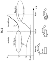
- a capacitance detection sensor as a first embodiment of the present invention illustrated in FIG. 1 includes a base material 10, a pair of first electrodes 111 and 112, a pair of second electrodes 121 and 122, and an electrostatic shielding member 140.
- a capacitance detection sensor module according to the first embodiment of the present invention includes the capacitance detection sensor according to the first embodiment of the present invention and a detection processing device 200.
- the electrostatic shielding member 140 may be omitted.
- the base material 10 is made of a dielectric such as PVC gel, polyvinylidene fluoride (PVDF), polydimethylsiloxane (PDMS), a silicon-based resin, a urethane-based resin, or epoxy-based resin, or a composite material of any combination thereof.
- the pair of first electrodes 111 and 112 is arranged apart from each other in a direction parallel to a contact surface 102 of the base material 10, and is embedded in the base material 10 with a gap interposed between the first electrodes and a dielectric constituting the base material 10 in a direction in which the sensitivity in the shearing direction needs to be increased.
- the pair of second electrodes 121 and 122 is embedded in the base material 10 so as to face each other at a position farther from the contact surface 102 of the base material 10 than the pair of first electrodes 111 and 112 in a direction perpendicular to the contact surface 102 of the base material 10.
- the electrostatic shielding member 140 is arranged between the pair of first electrodes 111 and 112 and the pair of second electrodes 121 and 122 so as to at least partially overlap each of the pair of first electrodes 111 and 112 and the pair of second electrodes 121 and 122 as seen in the direction perpendicular to the contact surface 102 of the base material 10, and is embedded in the base material 10 in a grounded state.
- the pair of first electrodes 111 and 112, the pair of second electrodes 121 and 122, and the electrostatic shielding member 140 are each made of a metal such as carbon, silver, gold, or a liquid metal, a conductive resin such as a thiophene-based conductive polymer or PSS, PVC gel, polyvinylidene fluoride (PVDF), polydimethylsiloxane (PDMS), a silicon-based resin, a urethane-based resin, or an epoxy-based resin, or a dielectric such as a composite material of any combination thereof, or a composite material of any combination thereof.
- a metal such as carbon, silver, gold, or a liquid metal
- a conductive resin such as a thiophene-based conductive polymer or PSS, PVC gel, polyvinylidene fluoride (PVDF), polydimethylsiloxane (PDMS), a silicon-based resin, a urethane-based resin, or an epoxy-based
- the capacitance detection sensor may be produced by forming each of the first electrodes 111 and 112, the second electrodes 121 and 122, and the electrostatic shielding member 140 by a conductive paste printed in a predetermined pattern on a sheet of a dielectric, and then stacking and integrating the plurality of dielectric sheets.
- the detection processing device 200 is configured by a computer including a microprocessor, a memory, and the like.
- the detection processing device 200 includes a first capacitance measurement element 210, a second capacitance measurement element 220, and a state determination element 240.
- the first capacitance measurement element 210 applies a voltage between the pair of first electrodes 111 and 112, and measures the potential difference between the pair of first electrodes 111 and 112 at this time, and thus the capacitance C1.
- the state determination element 240 detects the proximity state of an object Q with respect to the contact surface 102 of the base material 10 according to the measurement result of the capacitance C1 between the pair of first electrodes 111 and 112.
- the second capacitance measurement element 220 applies a voltage between the pair of second electrodes 121 and 122, and measures the potential difference between the pair of second electrodes 121 and 122 at this time, and thus the capacitance C2.
- the state determination element 240 detects the pressure acting on the base material 10 from the object Q in contact with the contact surface 102 of the base material 10 according to the measurement result of the capacitance C2 between the pair of second electrodes 121 and 122.
- a voltage is applied between the pair of first electrodes 111 and 112 (see the lines of electric force represented by the curved arrows in FIG. 1 ), and the capacitance C1 between the pair of first electrodes 111 and 112 is measured based on the potential difference between the pair of first electrodes 111 and 112 at this time.
- a voltage is applied between the pair of second electrodes 121 and 122 (see the lines of electric force represented by the upward arrows in FIG. 1 ), and the capacitance C2 between the pair of second electrodes 121 and 122 is measured based on the potential difference between the pair of second electrodes 121 and 122 at this time.
- a voltage may be applied to the pair of second electrodes 121 and 122 such that the lower second electrode 121 has a higher potential than the upper second electrode 122, or a voltage may be applied to the pair of second electrodes 121 and 122 such that the lower second electrode 121 has a lower potential than the upper second electrode 122.
- a plurality of states is determined on the basis of a capacitance value Cp between the pair of first electrodes 111 and 112 in a state where the object Q that is a part of a human body such as a finger of a hand is not in proximity to and in contact with the base material 10, a capacitance value Cp_min between the pair of first electrodes 111 and 112 in a state where the object Q is in contact with the base material 10, and a capacitance value Cf between the pair of second electrodes 121 and 122 in a state where there is no pressure from the object Q on the base material 10.
- Table 1 collectively shows the measurement results of the capacitance C1 between the pair of first electrodes 111 and 112 and the determination results of the states according to the measurement results of the capacitance C2 between the pair of second electrodes 121 and 122.
- FIG. 2 illustrates change modes of the capacitance C1 between the pair of first electrodes 111 and 112 and the capacitance C2 between the pair of second electrodes 121 and 122 with the state transitions from (1) to (5).
- the electrostatic shielding member 140 it is possible to avoid a reduction in the measurement accuracy of the capacitance C2 between the pair of second electrodes 121 and 122 due to the electrostatic interaction between the object Q approaching the base material 10 and the pair of second electrodes 121 and 122, thereby improving the determination accuracy of each state.
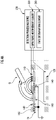
- a capacitance detection sensor as a second embodiment of the present invention illustrated in FIG. 3 includes a base material 10, a reference electrode 100, a first electrode 110, and a second electrode 120.
- a capacitance detection sensor module according to the second embodiment of the present invention includes the capacitance detection sensor according to the second embodiment of the present invention and a detection processing device 200.
- the electrostatic shielding member 140 may be omitted.
- the base material 10 is made of a dielectric such as PVC gel, polyvinylidene fluoride (PVDF), polydimethylsiloxane (PDMS), a silicon-based resin, a urethane-based resin, or epoxy-based resin, or a composite material of any combination thereof.
- the reference electrode 100 and the first electrode 110 are arranged apart from each other in a direction parallel to a contact surface 102 of the base material 10, and is embedded in the base material 10 with a gap interposed between the first electrodes and a dielectric constituting the base material 10 in a direction in which the sensitivity in the shearing direction needs to be increased.
- the second electrode 120 is embedded in the base material 10 so as to face the reference electrode 100 at a position farther from the contact surface 102 of the base material 10 than the first electrode 110 in a direction perpendicular to the contact surface 102 of the base material 10.
- the electrostatic shielding member 140 is arranged between the reference electrode 100 and the first electrode 110 in a direction parallel to the contact surface 102 of the base material 10, and is embedded in the base material 10 in a grounded state.
- the reference electrode 100, the first electrode 110, the second electrode 120, and the electrostatic shielding member 140 are each made of a metal such as carbon, silver, gold, or a liquid metal, a conductive resin such as a thiophene-based conductive polymer or PSS, PVC gel, polyvinylidene fluoride (PVDF), polydimethylsiloxane (PDMS), a silicon-based resin, a urethane-based resin, or an epoxy-based resin, or a dielectric such as a composite material of any combination thereof, or a composite material of any combination thereof.
- a metal such as carbon, silver, gold, or a liquid metal
- a conductive resin such as a thiophene-based conductive polymer or PSS, PVC gel, polyvinylidene fluoride (PVDF), polydimethylsiloxane (PDMS), a silicon-based resin, a urethane-based resin, or an epoxy-based resin, or a dielectric such
- the capacitance detection sensor may be produced by forming each of the reference electrode 100, the first electrode 110, the second electrode 120, and the electrostatic shielding member 140 by a conductive paste printed in a predetermined pattern on a sheet of a dielectric, and then stacking and integrating the plurality of dielectric sheets.
- the pair of first electrodes 111 and 112, the one second electrode 122, and the other second electrodes 121 are arranged at three places or on three layers having different distances from the contact surface 102 of the base material 10 (see FIG. 1 ).
- the reference electrode 100, the first electrode 110, and the second electrode 120 are arranged at two places or on two layers having different distances from the surface 102 (see FIG. 3 ). Therefore, in the second embodiment, the arrangement space of the plurality of electrodes can be made compact and the capacitance detection sensor can be made thinner than in the first embodiment in the direction perpendicular to the contact surface 102 of the base material 10.
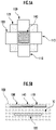
- an existing configuration in which five substantially square electrodes are arranged in a cross shape and buried in a first layer of the base material 10, and a substantially square electrode having a large area is buried in a second layer of the base material 10 so as to overlap the five substantially square electrodes will be considered.
- the central electrode arranged in the first layer may be used as the electrostatic shielding member 140
- the first pair of electrodes adjacent to the central electrode may be used as the reference electrode 100
- the second pair of electrodes adjacent to the central electrode may be used as the first electrode 110
- the electrode arranged in the second layer may be used as the second electrode 120.
- the detection processing device 200 is configured by a computer including a microprocessor, a memory, and the like.
- the detection processing device 200 includes a capacitance measurement element 230 and a state determination element 240.
- the capacitance measurement element 230 alternately switches between a first detection period in which a voltage is applied between the reference electrode 100 and the first electrode 110 and a second detection period in which a voltage is applied between the reference electrode 100 and the second electrode 120.
- the capacitance measurement element 230 measures a capacitance C1 between the reference electrode 100 and the first electrode 110 in the first detection period.
- the state determination element 240 detects the proximity state of an object Q with respect to the contact surface 102 of the base material 10 according to the measurement result.
- the capacitance measurement element 230 measures a capacitance C2 between the reference electrode 100 and the second electrode 120 in the second detection period.
- the state determination element 240 detects the pressure acting on the base material 10 from the object Q in contact with the contact surface 102 of the base material 10 according to the measurement result.
- a voltage is applied between the reference electrode 100 and the first electrode 110 in the first detection period (see the lines of electric force represented by the curved arrows in FIG. 4A ).
- a voltage may be applied between the reference electrode 100 and the first electrode 110 such that the reference electrode 100 has a higher potential than the first electrode 110, or a voltage may be applied between the reference electrode 100 and the first electrode 110 such that the reference electrode 100 has a lower potential than the first electrode 110.
- the potential difference between the reference electrode 100 and the first electrode 110, and eventually, the capacitance C1 are measured.
- a voltage is applied between the reference electrode 100 and the second electrode 120 (see the lines of electric force represented by the downward arrows in FIG. 4B ).
- a voltage may be applied between the reference electrode 100 and the second electrode 120 such that the reference electrode 100 has a higher potential than the second electrode 120, or a voltage may be applied between the reference electrode 100 and the second electrode 120 such that the reference electrode 100 has a lower potential than the second electrode 120.
- the potential difference between the reference electrode 100 and the second electrode 120, and eventually the capacitance C2 are measured.
- a plurality of states is determined on the basis of a capacitance value Cp between the reference electrode 100 and the first electrode 110 in a state where the object Q is not in proximity to and in contact with the base material 10, a capacitance value Cp_min between the reference electrode 100 and the first electrode 110 in a state where the object is in contact with the base material 10, and a capacitance value Cf between the reference electrode 100 and the second electrode 120 in a state where there is no pressure from the object on the base material 10.
- This determination method is similar to the determination method of the first embodiment shown in Table 1.
- the electrostatic shielding member 140 it is possible to avoid a reduction in the measurement accuracy of the capacitance C2 between the reference electrode 100 and the second electrode 120 due to the electrostatic interaction between the object Q approaching the base material 10 and the second electrode 120, thereby improving the determination accuracy of each state.
- an average distance d between all the fingers and the object is 0 while all the fingers stroke the object, and then gradually increases as some of the fingers move away from the object.
- an average shear force f applied from the finger to the object is substantially constant while all the fingers stroke the object, and then gradually decreases as some of the fingers move away from the object, and becomes 0 when all the fingers move away from the object.
- the capacitance detection sensors as the first embodiment of the present invention are arranged on the surface of the object, as indicated by the one-dot chain line in FIG. 7A , the total value of the capacitance C1 between the pair of first electrodes 111 and 112 is 0 while all the fingers stroke the object, and then gradually increases as some of the fingers move away from the object, and is saturated at a certain value.
- the two-dot chain line in FIG. 7A the total value of the capacitance C1 between the pair of first electrodes 111 and 112 is 0 while all the fingers stroke the object, and then gradually increases as some of the fingers move away from the object, and is saturated at a certain value.
- the total value of the capacitance C2 between the pair of second electrodes 121 and 122 is substantially constant while all the fingers stroke the object, and then gradually decreases when some of the fingers move away from the object, and converges to a constant value when all the fingers are separated from the object by a predetermined distance or more.
- the total value of the intermittent capacitance C1 between the reference electrode 100 and the first electrode 110 in the first detection period is 0 while all the fingers stroke the object, and then gradually increases as some of the fingers move away from the object, and is saturated at a certain value.
- the two-dot chain line in FIG. 7B indicates that the two-dot chain line in FIG.
- the total value of the intermittent capacitance C2 between the reference electrode 100 and the second electrode 120 in the second detection period is substantially constant while all the fingers stroke the object, and then gradually decreases when some of the fingers move away from the object, and converges to a constant value when all the fingers are separated from the object by a predetermined distance or more.
- the pair of first electrodes 111 and 112 is entirely embedded in the base material 10 in a state of being separated from each other in the direction parallel to the contact surface 102 of the base material 10 (see FIG. 2 ).
- at least one of the pair of first electrodes 111 and 112 may be attached to the surface of the base material 10 or partially embedded in the base material 10 so as to be partially exposed (for example, one main surface of the plate electrode is exposed).
- the pair of first electrodes 111 and 112 do not need to be separated from each other in the parallel direction as long as the lines of electric force that are three-dimensionally separated and connect the electrodes pass through the contact surface 102 of the dielectric.
- the exposed portion may be protected by an insulating sheet.
- the pair of second electrodes 121 and 122 are both entirely embedded in the base material 10 (see FIG. 1 ).
- at least one of the pair of second electrodes 121 and 122 may be attached to the surface of the base material 10 or partially embedded in the base material 10 so as to be partially exposed (for example, a part of one main surface of the flat plate electrode is exposed). The exposed portion may be protected by an insulating sheet.
- the reference electrode 100, the first electrode 110, and the second electrode 120 are all entirely embedded in the base material 10 (see FIG. 3 ).
- at least one of the electrodes may be attached to the surface of the base material 10 or partially embedded in the base material 10 so as to be partially exposed (for example, one main surface of the flat plate electrode is exposed). The exposed portion may be protected by an insulating sheet.
Landscapes
- Physics & Mathematics (AREA)
- General Physics & Mathematics (AREA)
- Life Sciences & Earth Sciences (AREA)
- Engineering & Computer Science (AREA)
- Remote Sensing (AREA)
- Geophysics (AREA)
- Geology (AREA)
- General Life Sciences & Earth Sciences (AREA)
- Environmental & Geological Engineering (AREA)
- Electromagnetism (AREA)
- Power Engineering (AREA)
- Geophysics And Detection Of Objects (AREA)
- Switches That Are Operated By Magnetic Or Electric Fields (AREA)
- Electronic Switches (AREA)
- Force Measurement Appropriate To Specific Purposes (AREA)
- Measurement Of Length, Angles, Or The Like Using Electric Or Magnetic Means (AREA)
Applications Claiming Priority (2)
| Application Number | Priority Date | Filing Date | Title |
|---|---|---|---|
| JP2019182941A JP7216963B2 (ja) | 2019-10-03 | 2019-10-03 | 静電容量型検知センサ、静電容量型検知センサモジュールおよび静電容量型検知センサを用いた状態判定方法 |
| PCT/JP2020/028929 WO2021065177A1 (ja) | 2019-10-03 | 2020-07-28 | 静電容量型検知センサ、静電容量型検知センサモジュールおよび静電容量型検知センサを用いた状態判定方法 |
Publications (3)
| Publication Number | Publication Date |
|---|---|
| EP4040459A1 true EP4040459A1 (de) | 2022-08-10 |
| EP4040459A4 EP4040459A4 (de) | 2022-11-23 |
| EP4040459B1 EP4040459B1 (de) | 2024-04-24 |
Family
ID=75338108
Family Applications (1)
| Application Number | Title | Priority Date | Filing Date |
|---|---|---|---|
| EP20871933.6A Active EP4040459B1 (de) | 2019-10-03 | 2020-07-28 | Kapazitätserfassungssensor, kapazitätserfassungssensormodul und zustandsbestimmungsverfahren mit kapazitätserfassungssensor |
Country Status (5)
| Country | Link |
|---|---|
| US (1) | US12117354B2 (de) |
| EP (1) | EP4040459B1 (de) |
| JP (2) | JP7216963B2 (de) |
| CN (1) | CN114450560B (de) |
| WO (1) | WO2021065177A1 (de) |
Families Citing this family (2)
| Publication number | Priority date | Publication date | Assignee | Title |
|---|---|---|---|---|
| JP7024908B1 (ja) * | 2021-05-06 | 2022-02-24 | 三菱電機株式会社 | 静電容量ボタン |
| CN117524791A (zh) * | 2021-05-06 | 2024-02-06 | 三菱电机株式会社 | 静电电容按钮 |
Family Cites Families (17)
| Publication number | Priority date | Publication date | Assignee | Title |
|---|---|---|---|---|
| US5682788A (en) * | 1995-07-12 | 1997-11-04 | Netzer; Yishay | Differential windshield capacitive moisture sensor |
| JPWO2006100725A1 (ja) * | 2005-03-18 | 2008-08-28 | ニッタ株式会社 | 静電容量式センサ |
| JP2008203055A (ja) * | 2007-02-20 | 2008-09-04 | Omron Corp | 静電容量センサ |
| US8692565B2 (en) * | 2007-10-04 | 2014-04-08 | Fujikura Ltd. | Capacitive proximity sensor and proximity sensing method |
| JP2010133791A (ja) * | 2008-12-03 | 2010-06-17 | Hitachi Cable Ltd | シート状センサ装置 |
| JP5609907B2 (ja) * | 2011-05-25 | 2014-10-22 | 株式会社デンソー | 乗員検知センサ |
| JP5748274B2 (ja) * | 2011-07-08 | 2015-07-15 | 株式会社ワコム | 位置検出センサ、位置検出装置および位置検出方法 |
| JP5888686B2 (ja) | 2012-11-26 | 2016-03-22 | 学校法人福岡大学 | 近接・接触センサ |
| JP2014119306A (ja) | 2012-12-14 | 2014-06-30 | Denso Corp | 荷重検出セル、荷重検出セルの製造方法および乗員検知センサ |
| EP2950190B1 (de) * | 2013-07-30 | 2019-05-22 | Sumitomo Riko Company Limited | Vorrichtung zur eingabezustandserfassung |
| DE102014107559A1 (de) * | 2014-05-28 | 2015-12-03 | Huf Hülsbeck & Fürst Gmbh & Co. Kg | Sensoreinrichtung für ein Kraftfahrzeug |
| US10724908B2 (en) | 2014-12-03 | 2020-07-28 | University Of British Columbia | Flexible transparent sensor with ionically-conductive material |
| JP6585907B2 (ja) | 2015-03-17 | 2019-10-02 | ローム株式会社 | 静電スイッチコントローラおよびその制御方法、ドア開閉装置、および電子キーシステム |
| US20180326456A1 (en) * | 2015-11-06 | 2018-11-15 | Moda-Innochips Co., Ltd. | Pressure sensor, and composite element and electronic device having same |
| KR20170056450A (ko) * | 2015-11-13 | 2017-05-23 | 주식회사 모다이노칩 | 복합 소자 및 이를 구비하는 전자기기 |
| CN111051834A (zh) * | 2017-07-10 | 2020-04-21 | 小利兰·斯坦福大学托管委员会 | 电容式和触觉传感器及相关感测方法 |
| KR102745345B1 (ko) * | 2018-10-23 | 2024-12-20 | 삼성전자주식회사 | 변형가능한 지문 인식 소자, 이를 이용한 지문 인증 방법 및 전자 장치 |
-
2019
- 2019-10-03 JP JP2019182941A patent/JP7216963B2/ja active Active
-
2020
- 2020-07-28 CN CN202080068170.7A patent/CN114450560B/zh active Active
- 2020-07-28 WO PCT/JP2020/028929 patent/WO2021065177A1/ja not_active Ceased
- 2020-07-28 EP EP20871933.6A patent/EP4040459B1/de active Active
- 2020-07-28 US US17/764,725 patent/US12117354B2/en active Active
-
2022
- 2022-12-13 JP JP2022198366A patent/JP2023051944A/ja active Pending
Also Published As
| Publication number | Publication date |
|---|---|
| US20220316964A1 (en) | 2022-10-06 |
| US12117354B2 (en) | 2024-10-15 |
| JP7216963B2 (ja) | 2023-02-02 |
| CN114450560B (zh) | 2024-04-30 |
| EP4040459B1 (de) | 2024-04-24 |
| WO2021065177A1 (ja) | 2021-04-08 |
| JP2023051944A (ja) | 2023-04-11 |
| CN114450560A (zh) | 2022-05-06 |
| EP4040459A4 (de) | 2022-11-23 |
| JP2021060211A (ja) | 2021-04-15 |
Similar Documents
| Publication | Publication Date | Title |
|---|---|---|
| CN102193699B (zh) | 传感设备和显示设备 | |
| US7679376B2 (en) | Capacitive sensor for sensing tactile and proximity, and a sensing system using the same | |
| US9696223B2 (en) | Single layer force sensor | |
| US8184106B2 (en) | Position detection device | |
| EP3073236B1 (de) | Drucksensor | |
| JP2013015976A (ja) | 多機能センサ | |
| US20100230181A1 (en) | Input device | |
| US20120218221A1 (en) | Touch panel device | |
| US11740141B2 (en) | Pressure-sensitive element | |
| US10509523B2 (en) | Methods and apparatus for a capacitive pressure sensor | |
| US10127835B2 (en) | Capacitive touch sensor | |
| JP7232263B2 (ja) | 感圧タッチセンサ及び感圧タッチセンサモジュール | |
| US12117354B2 (en) | Capacitance detection sensor, capacitance detection sensor module and state determination method using capacitance detection sensor | |
| CN103264674A (zh) | 一种座椅乘员占用传感器 | |
| JP2018115873A (ja) | センサシート | |
| US20220252471A1 (en) | A capacitive touch and pressure sensor | |
| CN105404430A (zh) | 3d压感触摸屏及其制造方法以及3d压感触控实现方法 | |
| US20230064769A1 (en) | Pressure sensor | |
| US11906372B2 (en) | Capacitance sensor and measurement device | |
| US11740150B2 (en) | Electrostatic capacity sensor | |
| KR20150096318A (ko) | 압력 센서 및 스타일러스 펜 | |
| JP5490043B2 (ja) | 乗員検知装置 | |
| US20250216992A1 (en) | Input Device | |
| US11630006B1 (en) | Vehicle surface force sensor | |
| WO2025084058A1 (ja) | せん断力検出装置 |
Legal Events
| Date | Code | Title | Description |
|---|---|---|---|
| STAA | Information on the status of an ep patent application or granted ep patent |
Free format text: STATUS: THE INTERNATIONAL PUBLICATION HAS BEEN MADE |
|
| PUAI | Public reference made under article 153(3) epc to a published international application that has entered the european phase |
Free format text: ORIGINAL CODE: 0009012 |
|
| STAA | Information on the status of an ep patent application or granted ep patent |
Free format text: STATUS: REQUEST FOR EXAMINATION WAS MADE |
|
| 17P | Request for examination filed |
Effective date: 20220324 |
|
| AK | Designated contracting states |
Kind code of ref document: A1 Designated state(s): AL AT BE BG CH CY CZ DE DK EE ES FI FR GB GR HR HU IE IS IT LI LT LU LV MC MK MT NL NO PL PT RO RS SE SI SK SM TR |
|
| A4 | Supplementary search report drawn up and despatched |
Effective date: 20221025 |
|
| RIC1 | Information provided on ipc code assigned before grant |
Ipc: H03K 17/96 20060101ALI20221019BHEP Ipc: H03K 17/975 20060101ALI20221019BHEP Ipc: G01V 3/08 20060101ALI20221019BHEP Ipc: H03K 17/955 20060101ALI20221019BHEP Ipc: G01D 5/241 20060101ALI20221019BHEP Ipc: H01H 36/00 20060101AFI20221019BHEP |
|
| DAV | Request for validation of the european patent (deleted) | ||
| DAX | Request for extension of the european patent (deleted) | ||
| STAA | Information on the status of an ep patent application or granted ep patent |
Free format text: STATUS: EXAMINATION IS IN PROGRESS |
|
| 17Q | First examination report despatched |
Effective date: 20230707 |
|
| GRAP | Despatch of communication of intention to grant a patent |
Free format text: ORIGINAL CODE: EPIDOSNIGR1 |
|
| STAA | Information on the status of an ep patent application or granted ep patent |
Free format text: STATUS: GRANT OF PATENT IS INTENDED |
|
| RAP3 | Party data changed (applicant data changed or rights of an application transferred) |
Owner name: THE UNIVERSITY OF BRITISH COLUMBIA Owner name: HONDA MOTOR CO., LTD. |
|
| INTG | Intention to grant announced |
Effective date: 20231218 |
|
| GRAS | Grant fee paid |
Free format text: ORIGINAL CODE: EPIDOSNIGR3 |
|
| GRAA | (expected) grant |
Free format text: ORIGINAL CODE: 0009210 |
|
| STAA | Information on the status of an ep patent application or granted ep patent |
Free format text: STATUS: THE PATENT HAS BEEN GRANTED |
|
| AK | Designated contracting states |
Kind code of ref document: B1 Designated state(s): AL AT BE BG CH CY CZ DE DK EE ES FI FR GB GR HR HU IE IS IT LI LT LU LV MC MK MT NL NO PL PT RO RS SE SI SK SM TR |
|
| REG | Reference to a national code |
Ref country code: GB Ref legal event code: FG4D |
|
| REG | Reference to a national code |
Ref country code: CH Ref legal event code: EP |
|
| REG | Reference to a national code |
Ref country code: DE Ref legal event code: R096 Ref document number: 602020029799 Country of ref document: DE |
|
| REG | Reference to a national code |
Ref country code: IE Ref legal event code: FG4D |
|
| REG | Reference to a national code |
Ref country code: LT Ref legal event code: MG9D |
|
| REG | Reference to a national code |
Ref country code: NL Ref legal event code: MP Effective date: 20240424 |
|
| REG | Reference to a national code |
Ref country code: AT Ref legal event code: MK05 Ref document number: 1680556 Country of ref document: AT Kind code of ref document: T Effective date: 20240424 |
|
| PG25 | Lapsed in a contracting state [announced via postgrant information from national office to epo] |
Ref country code: NL Free format text: LAPSE BECAUSE OF FAILURE TO SUBMIT A TRANSLATION OF THE DESCRIPTION OR TO PAY THE FEE WITHIN THE PRESCRIBED TIME-LIMIT Effective date: 20240424 |
|
| PG25 | Lapsed in a contracting state [announced via postgrant information from national office to epo] |
Ref country code: NL Free format text: LAPSE BECAUSE OF FAILURE TO SUBMIT A TRANSLATION OF THE DESCRIPTION OR TO PAY THE FEE WITHIN THE PRESCRIBED TIME-LIMIT Effective date: 20240424 |
|
| PG25 | Lapsed in a contracting state [announced via postgrant information from national office to epo] |
Ref country code: IS Free format text: LAPSE BECAUSE OF FAILURE TO SUBMIT A TRANSLATION OF THE DESCRIPTION OR TO PAY THE FEE WITHIN THE PRESCRIBED TIME-LIMIT Effective date: 20240824 |
|
| PG25 | Lapsed in a contracting state [announced via postgrant information from national office to epo] |
Ref country code: BG Free format text: LAPSE BECAUSE OF FAILURE TO SUBMIT A TRANSLATION OF THE DESCRIPTION OR TO PAY THE FEE WITHIN THE PRESCRIBED TIME-LIMIT Effective date: 20240424 |
|
| PG25 | Lapsed in a contracting state [announced via postgrant information from national office to epo] |
Ref country code: HR Free format text: LAPSE BECAUSE OF FAILURE TO SUBMIT A TRANSLATION OF THE DESCRIPTION OR TO PAY THE FEE WITHIN THE PRESCRIBED TIME-LIMIT Effective date: 20240424 Ref country code: FI Free format text: LAPSE BECAUSE OF FAILURE TO SUBMIT A TRANSLATION OF THE DESCRIPTION OR TO PAY THE FEE WITHIN THE PRESCRIBED TIME-LIMIT Effective date: 20240424 |
|
| PG25 | Lapsed in a contracting state [announced via postgrant information from national office to epo] |
Ref country code: GR Free format text: LAPSE BECAUSE OF FAILURE TO SUBMIT A TRANSLATION OF THE DESCRIPTION OR TO PAY THE FEE WITHIN THE PRESCRIBED TIME-LIMIT Effective date: 20240725 |
|
| PG25 | Lapsed in a contracting state [announced via postgrant information from national office to epo] |
Ref country code: PT Free format text: LAPSE BECAUSE OF FAILURE TO SUBMIT A TRANSLATION OF THE DESCRIPTION OR TO PAY THE FEE WITHIN THE PRESCRIBED TIME-LIMIT Effective date: 20240826 |
|
| PG25 | Lapsed in a contracting state [announced via postgrant information from national office to epo] |
Ref country code: ES Free format text: LAPSE BECAUSE OF FAILURE TO SUBMIT A TRANSLATION OF THE DESCRIPTION OR TO PAY THE FEE WITHIN THE PRESCRIBED TIME-LIMIT Effective date: 20240424 |
|
| PG25 | Lapsed in a contracting state [announced via postgrant information from national office to epo] |
Ref country code: AT Free format text: LAPSE BECAUSE OF FAILURE TO SUBMIT A TRANSLATION OF THE DESCRIPTION OR TO PAY THE FEE WITHIN THE PRESCRIBED TIME-LIMIT Effective date: 20240424 |
|
| PG25 | Lapsed in a contracting state [announced via postgrant information from national office to epo] |
Ref country code: PL Free format text: LAPSE BECAUSE OF FAILURE TO SUBMIT A TRANSLATION OF THE DESCRIPTION OR TO PAY THE FEE WITHIN THE PRESCRIBED TIME-LIMIT Effective date: 20240424 |
|
| PG25 | Lapsed in a contracting state [announced via postgrant information from national office to epo] |
Ref country code: LV Free format text: LAPSE BECAUSE OF FAILURE TO SUBMIT A TRANSLATION OF THE DESCRIPTION OR TO PAY THE FEE WITHIN THE PRESCRIBED TIME-LIMIT Effective date: 20240424 |
|
| PG25 | Lapsed in a contracting state [announced via postgrant information from national office to epo] |
Ref country code: PT Free format text: LAPSE BECAUSE OF FAILURE TO SUBMIT A TRANSLATION OF THE DESCRIPTION OR TO PAY THE FEE WITHIN THE PRESCRIBED TIME-LIMIT Effective date: 20240826 Ref country code: PL Free format text: LAPSE BECAUSE OF FAILURE TO SUBMIT A TRANSLATION OF THE DESCRIPTION OR TO PAY THE FEE WITHIN THE PRESCRIBED TIME-LIMIT Effective date: 20240424 Ref country code: NO Free format text: LAPSE BECAUSE OF FAILURE TO SUBMIT A TRANSLATION OF THE DESCRIPTION OR TO PAY THE FEE WITHIN THE PRESCRIBED TIME-LIMIT Effective date: 20240724 Ref country code: LV Free format text: LAPSE BECAUSE OF FAILURE TO SUBMIT A TRANSLATION OF THE DESCRIPTION OR TO PAY THE FEE WITHIN THE PRESCRIBED TIME-LIMIT Effective date: 20240424 Ref country code: IS Free format text: LAPSE BECAUSE OF FAILURE TO SUBMIT A TRANSLATION OF THE DESCRIPTION OR TO PAY THE FEE WITHIN THE PRESCRIBED TIME-LIMIT Effective date: 20240824 Ref country code: HR Free format text: LAPSE BECAUSE OF FAILURE TO SUBMIT A TRANSLATION OF THE DESCRIPTION OR TO PAY THE FEE WITHIN THE PRESCRIBED TIME-LIMIT Effective date: 20240424 Ref country code: GR Free format text: LAPSE BECAUSE OF FAILURE TO SUBMIT A TRANSLATION OF THE DESCRIPTION OR TO PAY THE FEE WITHIN THE PRESCRIBED TIME-LIMIT Effective date: 20240725 Ref country code: FI Free format text: LAPSE BECAUSE OF FAILURE TO SUBMIT A TRANSLATION OF THE DESCRIPTION OR TO PAY THE FEE WITHIN THE PRESCRIBED TIME-LIMIT Effective date: 20240424 Ref country code: ES Free format text: LAPSE BECAUSE OF FAILURE TO SUBMIT A TRANSLATION OF THE DESCRIPTION OR TO PAY THE FEE WITHIN THE PRESCRIBED TIME-LIMIT Effective date: 20240424 Ref country code: BG Free format text: LAPSE BECAUSE OF FAILURE TO SUBMIT A TRANSLATION OF THE DESCRIPTION OR TO PAY THE FEE WITHIN THE PRESCRIBED TIME-LIMIT Effective date: 20240424 Ref country code: AT Free format text: LAPSE BECAUSE OF FAILURE TO SUBMIT A TRANSLATION OF THE DESCRIPTION OR TO PAY THE FEE WITHIN THE PRESCRIBED TIME-LIMIT Effective date: 20240424 Ref country code: RS Free format text: LAPSE BECAUSE OF FAILURE TO SUBMIT A TRANSLATION OF THE DESCRIPTION OR TO PAY THE FEE WITHIN THE PRESCRIBED TIME-LIMIT Effective date: 20240724 |
|
| PG25 | Lapsed in a contracting state [announced via postgrant information from national office to epo] |
Ref country code: DK Free format text: LAPSE BECAUSE OF FAILURE TO SUBMIT A TRANSLATION OF THE DESCRIPTION OR TO PAY THE FEE WITHIN THE PRESCRIBED TIME-LIMIT Effective date: 20240424 |
|
| PG25 | Lapsed in a contracting state [announced via postgrant information from national office to epo] |
Ref country code: EE Free format text: LAPSE BECAUSE OF FAILURE TO SUBMIT A TRANSLATION OF THE DESCRIPTION OR TO PAY THE FEE WITHIN THE PRESCRIBED TIME-LIMIT Effective date: 20240424 |
|
| PG25 | Lapsed in a contracting state [announced via postgrant information from national office to epo] |
Ref country code: CZ Free format text: LAPSE BECAUSE OF FAILURE TO SUBMIT A TRANSLATION OF THE DESCRIPTION OR TO PAY THE FEE WITHIN THE PRESCRIBED TIME-LIMIT Effective date: 20240424 |
|
| PG25 | Lapsed in a contracting state [announced via postgrant information from national office to epo] |
Ref country code: SK Free format text: LAPSE BECAUSE OF FAILURE TO SUBMIT A TRANSLATION OF THE DESCRIPTION OR TO PAY THE FEE WITHIN THE PRESCRIBED TIME-LIMIT Effective date: 20240424 Ref country code: RO Free format text: LAPSE BECAUSE OF FAILURE TO SUBMIT A TRANSLATION OF THE DESCRIPTION OR TO PAY THE FEE WITHIN THE PRESCRIBED TIME-LIMIT Effective date: 20240424 |
|
| REG | Reference to a national code |
Ref country code: DE Ref legal event code: R097 Ref document number: 602020029799 Country of ref document: DE |
|
| PG25 | Lapsed in a contracting state [announced via postgrant information from national office to epo] |
Ref country code: SM Free format text: LAPSE BECAUSE OF FAILURE TO SUBMIT A TRANSLATION OF THE DESCRIPTION OR TO PAY THE FEE WITHIN THE PRESCRIBED TIME-LIMIT Effective date: 20240424 |
|
| PG25 | Lapsed in a contracting state [announced via postgrant information from national office to epo] |
Ref country code: SM Free format text: LAPSE BECAUSE OF FAILURE TO SUBMIT A TRANSLATION OF THE DESCRIPTION OR TO PAY THE FEE WITHIN THE PRESCRIBED TIME-LIMIT Effective date: 20240424 Ref country code: SK Free format text: LAPSE BECAUSE OF FAILURE TO SUBMIT A TRANSLATION OF THE DESCRIPTION OR TO PAY THE FEE WITHIN THE PRESCRIBED TIME-LIMIT Effective date: 20240424 Ref country code: RO Free format text: LAPSE BECAUSE OF FAILURE TO SUBMIT A TRANSLATION OF THE DESCRIPTION OR TO PAY THE FEE WITHIN THE PRESCRIBED TIME-LIMIT Effective date: 20240424 Ref country code: EE Free format text: LAPSE BECAUSE OF FAILURE TO SUBMIT A TRANSLATION OF THE DESCRIPTION OR TO PAY THE FEE WITHIN THE PRESCRIBED TIME-LIMIT Effective date: 20240424 Ref country code: DK Free format text: LAPSE BECAUSE OF FAILURE TO SUBMIT A TRANSLATION OF THE DESCRIPTION OR TO PAY THE FEE WITHIN THE PRESCRIBED TIME-LIMIT Effective date: 20240424 Ref country code: CZ Free format text: LAPSE BECAUSE OF FAILURE TO SUBMIT A TRANSLATION OF THE DESCRIPTION OR TO PAY THE FEE WITHIN THE PRESCRIBED TIME-LIMIT Effective date: 20240424 |
|
| PG25 | Lapsed in a contracting state [announced via postgrant information from national office to epo] |
Ref country code: MC Free format text: LAPSE BECAUSE OF FAILURE TO SUBMIT A TRANSLATION OF THE DESCRIPTION OR TO PAY THE FEE WITHIN THE PRESCRIBED TIME-LIMIT Effective date: 20240424 |
|
| PLBE | No opposition filed within time limit |
Free format text: ORIGINAL CODE: 0009261 |
|
| STAA | Information on the status of an ep patent application or granted ep patent |
Free format text: STATUS: NO OPPOSITION FILED WITHIN TIME LIMIT |
|
| PG25 | Lapsed in a contracting state [announced via postgrant information from national office to epo] |
Ref country code: LU Free format text: LAPSE BECAUSE OF NON-PAYMENT OF DUE FEES Effective date: 20240728 |
|
| GBPC | Gb: european patent ceased through non-payment of renewal fee |
Effective date: 20240728 |
|
| PG25 | Lapsed in a contracting state [announced via postgrant information from national office to epo] |
Ref country code: LU Free format text: LAPSE BECAUSE OF NON-PAYMENT OF DUE FEES Effective date: 20240728 |
|
| 26N | No opposition filed |
Effective date: 20250127 |
|
| PG25 | Lapsed in a contracting state [announced via postgrant information from national office to epo] |
Ref country code: SI Free format text: LAPSE BECAUSE OF FAILURE TO SUBMIT A TRANSLATION OF THE DESCRIPTION OR TO PAY THE FEE WITHIN THE PRESCRIBED TIME-LIMIT Effective date: 20240424 Ref country code: BE Free format text: LAPSE BECAUSE OF NON-PAYMENT OF DUE FEES Effective date: 20240731 |
|
| PG25 | Lapsed in a contracting state [announced via postgrant information from national office to epo] |
Ref country code: FR Free format text: LAPSE BECAUSE OF NON-PAYMENT OF DUE FEES Effective date: 20240731 |
|
| PG25 | Lapsed in a contracting state [announced via postgrant information from national office to epo] |
Ref country code: GB Free format text: LAPSE BECAUSE OF NON-PAYMENT OF DUE FEES Effective date: 20240728 |
|
| REG | Reference to a national code |
Ref country code: BE Ref legal event code: MM Effective date: 20240731 |
|
| PG25 | Lapsed in a contracting state [announced via postgrant information from national office to epo] |
Ref country code: IE Free format text: LAPSE BECAUSE OF NON-PAYMENT OF DUE FEES Effective date: 20240728 |
|
| PG25 | Lapsed in a contracting state [announced via postgrant information from national office to epo] |
Ref country code: SE Free format text: LAPSE BECAUSE OF FAILURE TO SUBMIT A TRANSLATION OF THE DESCRIPTION OR TO PAY THE FEE WITHIN THE PRESCRIBED TIME-LIMIT Effective date: 20240424 |
|
| PGFP | Annual fee paid to national office [announced via postgrant information from national office to epo] |
Ref country code: DE Payment date: 20250509 Year of fee payment: 6 |
|
| PGFP | Annual fee paid to national office [announced via postgrant information from national office to epo] |
Ref country code: CH Payment date: 20250801 Year of fee payment: 6 |
|
| PG25 | Lapsed in a contracting state [announced via postgrant information from national office to epo] |
Ref country code: IT Free format text: LAPSE BECAUSE OF NON-PAYMENT OF DUE FEES Effective date: 20240728 |
|
| PG25 | Lapsed in a contracting state [announced via postgrant information from national office to epo] |
Ref country code: CY Free format text: LAPSE BECAUSE OF FAILURE TO SUBMIT A TRANSLATION OF THE DESCRIPTION OR TO PAY THE FEE WITHIN THE PRESCRIBED TIME-LIMIT; INVALID AB INITIO Effective date: 20200728 |
|
| PG25 | Lapsed in a contracting state [announced via postgrant information from national office to epo] |
Ref country code: HU Free format text: LAPSE BECAUSE OF FAILURE TO SUBMIT A TRANSLATION OF THE DESCRIPTION OR TO PAY THE FEE WITHIN THE PRESCRIBED TIME-LIMIT; INVALID AB INITIO Effective date: 20200728 |