EP4030468B1 - Verfahren zur herstellung einer luftbrücke - Google Patents
Verfahren zur herstellung einer luftbrücke Download PDFInfo
- Publication number
- EP4030468B1 EP4030468B1 EP21791237.7A EP21791237A EP4030468B1 EP 4030468 B1 EP4030468 B1 EP 4030468B1 EP 21791237 A EP21791237 A EP 21791237A EP 4030468 B1 EP4030468 B1 EP 4030468B1
- Authority
- EP
- European Patent Office
- Prior art keywords
- photoresist layer
- bridge
- photoresist
- bridge support
- substrate
- Prior art date
- Legal status (The legal status is an assumption and is not a legal conclusion. Google has not performed a legal analysis and makes no representation as to the accuracy of the status listed.)
- Active
Links
Images


Classifications
-
- H—ELECTRICITY
- H10—SEMICONDUCTOR DEVICES; ELECTRIC SOLID-STATE DEVICES NOT OTHERWISE PROVIDED FOR
- H10D—INORGANIC ELECTRIC SEMICONDUCTOR DEVICES
- H10D62/00—Semiconductor bodies, or regions thereof, of devices having potential barriers
- H10D62/10—Shapes, relative sizes or dispositions of the regions of the semiconductor bodies; Shapes of the semiconductor bodies
- H10D62/113—Isolations within a component, i.e. internal isolations
- H10D62/115—Dielectric isolations, e.g. air gaps
-
- H—ELECTRICITY
- H10—SEMICONDUCTOR DEVICES; ELECTRIC SOLID-STATE DEVICES NOT OTHERWISE PROVIDED FOR
- H10W—GENERIC PACKAGES, INTERCONNECTIONS, CONNECTORS OR OTHER CONSTRUCTIONAL DETAILS OF DEVICES COVERED BY CLASS H10
- H10W10/00—Isolation regions in semiconductor bodies between components of integrated devices
- H10W10/01—Manufacture or treatment
- H10W10/021—Manufacture or treatment of air gaps
-
- H—ELECTRICITY
- H10—SEMICONDUCTOR DEVICES; ELECTRIC SOLID-STATE DEVICES NOT OTHERWISE PROVIDED FOR
- H10W—GENERIC PACKAGES, INTERCONNECTIONS, CONNECTORS OR OTHER CONSTRUCTIONAL DETAILS OF DEVICES COVERED BY CLASS H10
- H10W10/00—Isolation regions in semiconductor bodies between components of integrated devices
- H10W10/20—Air gaps
-
- H—ELECTRICITY
- H10—SEMICONDUCTOR DEVICES; ELECTRIC SOLID-STATE DEVICES NOT OTHERWISE PROVIDED FOR
- H10W—GENERIC PACKAGES, INTERCONNECTIONS, CONNECTORS OR OTHER CONSTRUCTIONAL DETAILS OF DEVICES COVERED BY CLASS H10
- H10W20/00—Interconnections in chips, wafers or substrates
- H10W20/40—Interconnections external to wafers or substrates, e.g. back-end-of-line [BEOL] metallisations or vias connecting to gate electrodes
- H10W20/482—Interconnections external to wafers or substrates, e.g. back-end-of-line [BEOL] metallisations or vias connecting to gate electrodes for individual devices provided for in groups H10D8/00 - H10D48/00, e.g. for power transistors
- H10W20/483—Interconnections over air gaps, e.g. air bridges
-
- H—ELECTRICITY
- H10—SEMICONDUCTOR DEVICES; ELECTRIC SOLID-STATE DEVICES NOT OTHERWISE PROVIDED FOR
- H10W—GENERIC PACKAGES, INTERCONNECTIONS, CONNECTORS OR OTHER CONSTRUCTIONAL DETAILS OF DEVICES COVERED BY CLASS H10
- H10W44/00—Electrical arrangements for controlling or matching impedance
- H10W44/20—Electrical arrangements for controlling or matching impedance at high-frequency [HF] or radio frequency [RF]
Definitions
- This disclosure relates to the field of semiconductor, superconductor, quantum, and nanofabrication technologies, and in particular, to a method for manufacturing an air bridge, an air bridge, and an electronic device.
- an air bridge structure provides a low thermal resistance connection and a heat dissipation channel for the electrode lead.
- An air bridge is a circuit structure, which is an approach to implement crossconnection of planar circuits by a three-dimensional bridge structure. Because a medium between the bridge and the circuit is air (or vacuum), the medium is referred to as an air bridge or a vacuum bridge. A bridge support angle of the air bridge determines the stability of the air bridge. However, no solution for effectively adjusting a bridge support angle of an air bridge is provided in the related art. US5817446A provides a method for forming an airbridge for interconnecting metal contacts on an integrated circuit. The airbridge is formed by initially patterning a support photoresist between the metal contacts to be interconnected, over the metal contact to be crossed.
- the pattern support photoresist is flood exposed with UV light and subsequently baked at a relatively high temperature to cause the support photoresist to flow into a generally spherical shape.
- the airbridged metal lines are patterned over the spherically shaped support photoresist. Excess metallization is lifted off the support photoresist and the photoresist used to pattern the airbridge is removed, forming an airbridge with curvature along both its width and length.
- a fabricating process of a semiconductor device includes the steps of forming a first photoresist layer on a surface of a substrate so as to cover a gate electrode on the substrate, forming a second photoresist layer on the fist photoresist layer with an increased sensitivity, forming a third photoresist layer on the second photoresist layer with a reduced sensitivity, forming an opening in a photoresist structure thus formed of the first through third photoresist layers such that the opening exposes the gate electrode and such that the opening has a diameter that increases gradually from the first photoresist layer to the second photoresist layer.
- a low-resistance metal layer is deposited on the photoresist structure including the opening, such that the metal layer forms a low-resistance electrode on the gate electrode.
- US5408742A relates to an air bridge and an evaporative process for making air bridges.
- a first layer of photoresist is patterned to create two openings over the contacts to be connected, separated by a strip of photoresist.
- the photoresist strip is hard baked to allow it to soften and to cause further cross linking. The softening allows surface tension to reshape the photoresist strip to create a gradually sloping arcuate surface between contact openings upon which a metal layer of nearly constant thickness may be evaporated.
- JPH09270464A intends to facilitate the production of highly integrated circuits and an minute aerial wiring.
- the solution is as follows. To form an aerial wiring 50 by lift-off method, insulation films 42 and 43 are formed, overhang or undercut opening is formed in the insulation film, the opening with a resist 51 and a wiring metal 48 is deposited. Since the resist is along the overhang or undercut opening, the lift-off method can be applied easily although the resist film is made thinner for minute processing
- Embodiments of this disclosure provide a method for manufacturing an air bridge.
- the disclosure also provides, as examples not being part of the invention, an air bridge, and an electronic device, which can implement effective control and adjustment of a bridge support angle of an air bridge.
- the invention provides a method for manufacturing an air bridge, including: applying a first photoresist layer to a substrate; applying a second photoresist layer to the first photoresist layer; exposing, developing, and fixing the second photoresist layer, to form a patterned structure for depositing a bridge support on the second photoresist layer; etching away the first photoresist layer in a specified area through the patterned structure, to form a structure for blocking a deposition material from diffusing to a periphery on the substrate, the specified area including a projection area formed on the first photoresist layer by a top opening of the patterned structure; and depositing a bridge support structure on a surface of the substrate exposed after the first photoresist layer in the specified area is etched away, and forming an air bridge based on the bridge support structure.
- a first photoresist layer and a second photoresist layer are sequentially applied to a substrate, and the second photoresist layer is then exposed, developed, and fixed, to form a patterned structure for depositing a bridge support on the second photoresist layer, so as to etch away the first photoresist layer in a specified area through the patterned structure.
- the specified area includes a projection area formed on the first photoresist layer by a top opening of the patterned structure, during deposition of a bridge support structure on a surface of the substrate exposed after the first photoresist layer in the specified area is etched away, the first photoresist layer that has not been etched away can block a deposition material from diffusing to a periphery, and a degree of etching (such as an etching range) of the first photoresist layer in the projection area can also affect a blocking procedure of the deposition material, so as to implement effective control and adjustment of a bridge support angle of an air bridge.
- an air bridge is based on a bridge support made of photoresist.
- an air bridge is based on a bridge support made of a releasable deposition material (which is usually silicon dioxide).
- a releasable deposition material which is usually silicon dioxide.
- the shape of a bridge may be changed by heating reflux.
- the shape of a bridge arch is usually improved.
- the bridge arch of the air bridge using this manufacturing solution is relatively stable.
- the air bridge based on a bridge support made of a releasable deposition material has a shape the same as that of the bridge support, and with additional restriction by a coating process, the air bridge is usually trapezoidal.
- the air bridge is crucial to the stability of the remaining part. Due to different bridge support angles 105, the trapezoidal shape of a trapezoidal bridge varies greatly. However, the bridge support angle determines an approach angle (an angle between an approach 103 and the bridge pier 106).
- the bridge support angle 105 is equal to the approach angle. If the approach angle is excessively small, a bridge top 104 is prone to collapse. If the approach angle is excessively large, a part of the approach tends to be very thin due to particular directionality during evaporation coating, to cause a fracture at the approach. Therefore, generally, the trapezoidal bridge with the approach angle being a tilt of 35° to 50° is the most stable. Therefore, it is very important to modify the bridge support angle 105 to ensure the stability of the air bridge.
- a coating process such as deposition and evaporation of manufacturing a bridge support usually starts to be taken into consideration to adjust the bridge support angle.
- Various parameters such as temperature, speed, and vacuum degree during the coating are changed. If process parameters of the coating are fixed or adjustable ranges are restricted, it is very difficult to adjust the bridge support angle of the air bridge.
- an additional part such as a sample pan water cooling system and an infrared heating and baking system usually needs to be added to a device.
- the invention provides a new method for manufacturing an air bridge.
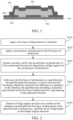
- the method includes the following steps:
- FIG. 2 The manufacturing method shown in FIG. 2 is described in detail below with reference to FIG. 3 to FIG. 8 .
- 301 is a substrate.
- a first photoresist layer 302 is applied to the substrate 301.
- a second photoresist layer 303 is applied to the first photoresist layer 302.
- a first baking may be performed on the first photoresist layer 302, to solidify the first photoresist layer 302 on the substrate 301 as soon as possible.
- the second photoresist layer 303 is applied to the first photoresist layer 302.
- a second baking may be performed on the second photoresist layer 303.
- a temperature of the second baking is less than or equal to a temperature of the first baking.
- the first photoresist layer 302 may be polymethyl methacrylate (PMMA).
- the second photoresist layer 303 may be an AZ negative photoresist.
- the second photoresist layer 303 is exposed as a pattern defining layer. After the exposure, as shown in FIG. 5 , the exposed second photoresist layer 303 is developed and fixed, to form a patterned structure 304 for depositing a bridge support on the second photoresist layer 303.
- the second photoresist layer 303 may be exposed through ultraviolet exposure or direct laser writing.
- a developer used for developing the second photoresist layer 303 may be a developer that do not cause a physical reaction or a chemical reaction with the first photoresist layer 302, so that the developer only develops the second photoresist layer 303.
- the first photoresist layer in a specified area 305 is etched away through the patterned structure 304, to form a structure (for clarity, refer to 306 in FIG. 7 for the structure) for blocking a deposition material from diffusing to a periphery on the substrate 301.
- the specified area 305 includes a projection area formed on the first photoresist layer 302 by a top opening of the patterned structure 304. In some embodiments, the specified area 305 may be the entire projection area, or the specified area 305 may be slightly larger than the projection area.
- a width of a bottom of the patterned structure 304 may be greater than a width of the top opening of the patterned structure 304, the bottom of the patterned structure 304 being in contact with the first photoresist layer 302.
- the surface of the substrate 301 may also form a structure protruding from the bottom of the patterned structure 304, to block the deposition material during deposition of the bridge support structure.
- a cross-section of the patterned structure 304 may be a regular trapezoid.
- a bridge support structure 307 is deposited on a surface of the exposed substrate, to form an air bridge based on the bridge support structure 307.
- a material of the bridge support structure 307 may be silicon dioxide.
- a thickness of the first photoresist layer 302 affects a height of the bridge support structure 307 that needs to be deposited.
- the thickness of the first photoresist layer 302 and the height of the bridge support structure 307 to be deposited satisfy the following conditions: 5 h ⁇ H ⁇ 6 h , where h represents the thickness of the first photoresist layer 302; and H represents the height of the bridge support structure 307 to be deposited.
- the second photoresist layer 303 and the first photoresist layer 302 on the substrate 301 may be removed after the bridge support structure 307 is deposited, to obtain the structure shown in FIG. 8 . Then overlaying and metal deposition may be performed on the structure based on FIG. 8 , to form the air bridge.
- the substrate that is, the structure shown in FIG. 7
- the substrate formed with the bridge support structure 307, the first photoresist layer 302, and the second photoresist layer 303 may be placed in a photoresist stripping solution, to remove the second photoresist layer 303 and the first photoresist layer 302.
- the structure shown in FIG. 7 may be directly placed in the same photoresist stripping solution. If the photoresist stripping solution for the first photoresist layer 302 is different from the photoresist stripping solution for the second photoresist layer 303, the structure shown in FIG. 7 is first placed in the photoresist stripping solution for the second photoresist layer 303. After the second photoresist layer 303 is removed, the substrate formed with the bridge support structure and the first photoresist layer 302 is placed in the photoresist stripping solution for the first photoresist layer 302.
- the bridge support angle obtained based on the technical solution in the embodiments of this disclosure is related to a position where the deposition material contacts the structure 306 when the deposition material diffuses, and is also related to a size of the opening formed through etching in the first photoresist layer 302.
- the bridge support angle is smaller.
- the opening is smaller (that is, the structure 306 protrudes more)
- the bridge support angle is larger.
- the size of the opening in the first photoresist layer 302 is related to an etching duration, that is, when the etching duration is longer, the opening is larger. When the etching duration is shorter, the opening is smaller.
- the bridge support angle may be modified by controlling the duration of etching the first photoresist layer 302.
- the etching duration of the first photoresist layer 302 is longer, the eventually obtained bridge support angle is smaller. Conversely, when the etching duration of the first photoresist layer 302 is shorter, the eventually obtained bridge support angle is larger.
- the method for manufacturing an air bridge may include the following steps:
- the bridge support structure manufactured by using the manufacturing method in the embodiments of this disclosure is shown in FIG. 9(b) , in which apparently the bridge support angle can be appropriately modified, and the bridge support angle can be increased, to make the bridge support angle in a state that ensures the stability of the air bridge.
- the bridge support angle of the bridge support structure manufactured by using the manufacturing method in the embodiments of this disclosure may reach about 37°.
- the bridge support angle of the bridge support structure manufactured in the related art is only about 22°.
- the etching duration also affects the final bridge support angle.
- FIG. 10(a) shows the bridge support structure obtained with a longer etching duration
- FIG. 10(b) shows the bridge support structure obtained with a shorter etching duration.
- the bridge support angle obtained in FIG. 10(a) is smaller than the bridge support angle obtained in FIG. 10(b) . That is, when the etching duration is longer, the bridge support angle of the obtained bridge support structure is smaller.
- the bridge support angle obtained with a longer etching duration is about 18°
- the bridge support angle obtained with a shorter etching duration is about 34°. Therefore, in embodiments of this disclosure, the bridge support angle of the air bridge can be modified by controlling the etching duration of the primer, thereby implementing effective control and adjustment of a bridge support angle of an air bridge.
- the air bridge manufactured by using the manufacturing method object of this invention has high stability, and can be used in various electronic circuits and electronic devices, such as in high frequency and ultra-high frequency devices, thereby greatly improving the working stability of electronic devices.
- the air bridge may also be used in superconducting quantum chip circuits, to provide a stable air bridge structure.
Landscapes
- Internal Circuitry In Semiconductor Integrated Circuit Devices (AREA)
- Drying Of Semiconductors (AREA)
- Micromachines (AREA)
Claims (11)
- Verfahren zur Herstellung einer Luftbrücke, umfassend:Aufbringen (S210) einer ersten Photoresistschicht (302) auf ein Substrat (301);Aufbringen (S220) einer zweiten Photoresistschicht (303) auf die erste Photoresistschicht (302);Belichten, Entwickeln und Fixieren (S230) der zweiten Photoresistschicht (303), um eine gemusterte Struktur (304) zum Aufbringen eines Brückenträgers auf der zweiten Photoresistschicht (303) zu bilden;Wegätzen (S240) der ersten Photoresistschicht (302) in einem spezifizierten Bereich (305) durch die gemusterte Struktur (304), um eine Struktur zu bilden, die ein Abscheidungsmaterial daran hindert, zu einer Peripherie auf dem Substrat zu diffundieren, wobei der spezifizierte Bereich (305) einen Projektionsbereich umfasst, der auf der ersten Photoresistschicht (302) durch eine obere Öffnung der gemusterten Struktur (304) gebildet wird;wobei das Verfahren gekennzeichnet ist durch Abscheiden (S250) einer Brückenträgerstruktur (307) auf einer Oberfläche des Substrats (301), die freiliegt, nachdem die erste Photoresistschicht (302) in dem spezifizierten Bereich (305) weggeätzt worden ist; undBilden (S250) der Luftbrücke auf der Basis der Brückenträgerstruktur (307).
- Verfahren zur Herstellung einer Luftbrücke nach Anspruch 1, wobei das Verfahren nach dem Aufbringen der ersten Photoresistschicht (302) auf das Substrat ferner umfasst:Durchführen eines ersten Backens der ersten Photoresistschicht (302); undnach dem Aufbringen der zweiten Photoresistschicht (303) auf die erste Photoresistschicht (302), das Verfahren ferner umfasst:
Durchführen eines zweiten Backens der zweiten Photoresistschicht (303), wobei eine Temperatur des zweiten Backens geringer oder gleich einer Temperatur des ersten Backens ist. - Verfahren zur Herstellung einer Luftbrücke nach Anspruch 1, wobei das Bilden der Luftbrücke auf der Basis der Brückenträgerstruktur (307) umfasst:Entfernen der zweiten Photoresistschicht (303) und der ersten Photoresistschicht (302) auf dem Substrat (301), nachdem die Brückenträgerstruktur (307) abgeschieden ist; undDurchführen einer Überlagerung und Metallabscheidung auf der Oberfläche des mit der Brückenträgerstruktur (307) gebildeten Substrats (301), nachdem die zweite Photoresistschicht (303) und die erste Photoresistschicht (302) auf dem Substrat (301) entfernt wurden, um die Luftbrücke zu bilden.
- Verfahren zur Herstellung einer Luftbrücke nach Anspruch 3, wobei das Entfernen der zweiten Photoresistschicht (303) und der ersten Photoresistschicht (302) auf dem Substrat (301) umfasst:
Anordnen des mit der Brückenträgerstruktur (307), der ersten Photoresistschicht (302) und der zweiten Photoresistschicht (303) gebildeten Substrats (301) in einer oder zwei Photoresistentfernerlösungen, Entfernen der zweiten Photoresistschicht (303) und der ersten Photoresistschicht (302). - Verfahren zur Herstellung einer Luftbrücke nach Anspruch 4, wobei es sich bei den Photoresistentfernerlösungen um eine erste Art einer Photoresistentfernerlösung für die erste Photoresistschicht (302) und eine zweite Art einer Entfernerlösung für die zweite Photoresistschicht (303) handelt, und die erste Art der Photoresistentfernerlösung für die erste Photoresistschicht (302) sich von der zweiten Art der Photoresistentfernerlösung für die zweite Photoresistschicht (303) unterscheidet, und das Anordnen des mit der Brückenträgerstruktur (307), der ersten Photoresistschicht (302) und der zweiten Photoresistschicht (303) gebildeten Substrats (301) in den zwei Photoresistentfernerlösungen umfasst:zuerst das Einbringen des mit der Brückenträgerstruktur (307) gebildeten Substrats (301), der ersten Photoresistschicht (302) und der zweiten Photoresistschicht (303) in die zweite Art der Photoresistentfernerlösung für die zweite Photoresistschicht (303); undnachdem die zweite Photoresistschicht (303) entfernt ist, Einlegen des mit der Brückenträgerstruktur (307) und der ersten Photoresistschicht (302) gebildeten Substrats (301) in die erste Art der Photoresistentfernerlösung für die erste Photoresistschicht (302).
- Verfahren zur Herstellung einer Luftbrücke nach Anspruch 1, wobei das Belichten, Entwickeln und Fixieren der zweiten Photoresistschicht (303) die Durchführung einer Ultraviolettbelichtung oder eines direkten Laserschreibens umfasst.
- Verfahren zur Herstellung einer Luftbrücke nach Anspruch 1, wobei eine Dicke der ersten Photoresistschicht (302) und eine Höhe der abzuscheidenden Brückenträgerstruktur (307) die folgenden Bedingungen erfüllen:

- Verfahren zur Herstellung einer Luftbrücke nach Anspruch 1, ferner umfassend:
Steuern eines Brückentragwinkels der Brückenträgerstruktur (307), die durch Abscheidung auf der Oberfläche des Substrats (301) erhalten wird, durch Steuern einer Ätzdauer der ersten Photoresistschicht (302) durch die gemusterte Struktur (304), wobei die Ätzdauer der ersten Photoresistschicht (302) durch die gemusterte Struktur (304) in einer umgekehrten Beziehung zu dem Brückentragwinkel der Brückenträgerstruktur (307) steht. - Verfahren zur Herstellung einer Luftbrücke nach Anspruch 1, wobei eine Breite eines Bodens der gemusterten Struktur (304) größer ist als eine Breite der oberen Öffnung der gemusterten Struktur (304), wobei der Boden der gemusterten Struktur (304) in Kontakt mit der ersten Photoresistschicht (302) steht.
- Verfahren zur Herstellung einer Luftbrücke nach Anspruch 9, wobei ein Querschnitt der gemusterten Struktur (304) ein regelmäßiges Trapez ist.
- Verfahren zur Herstellung einer Luftbrücke nach Anspruch 1, wobei das Belichten, Entwickeln und Fixieren der zweiten Photoresistschicht (303) zur Bildung der gemusterten Struktur (304) die Verwendung eines Entwicklers bei der Entwicklung der zweiten Photoresistschicht (303) umfasst, wobei der Entwickler nicht in der Lage ist, eine physikalische Reaktion oder eine chemische Reaktion mit der ersten Photoresistschicht (302) zu verursachen.
Applications Claiming Priority (2)
| Application Number | Priority Date | Filing Date | Title |
|---|---|---|---|
| CN202011288110.4A CN112103241B (zh) | 2020-11-17 | 2020-11-17 | 空气桥制作方法、空气桥及电子设备 |
| PCT/CN2021/102878 WO2022105232A1 (zh) | 2020-11-17 | 2021-06-28 | 空气桥制作方法、空气桥及电子设备 |
Publications (4)
| Publication Number | Publication Date |
|---|---|
| EP4030468A1 EP4030468A1 (de) | 2022-07-20 |
| EP4030468A4 EP4030468A4 (de) | 2022-07-20 |
| EP4030468B1 true EP4030468B1 (de) | 2023-12-06 |
| EP4030468C0 EP4030468C0 (de) | 2023-12-06 |
Family
ID=81586861
Family Applications (1)
| Application Number | Title | Priority Date | Filing Date |
|---|---|---|---|
| EP21791237.7A Active EP4030468B1 (de) | 2020-11-17 | 2021-06-28 | Verfahren zur herstellung einer luftbrücke |
Country Status (4)
| Country | Link |
|---|---|
| US (1) | US11996319B2 (de) |
| EP (1) | EP4030468B1 (de) |
| JP (1) | JP7304967B2 (de) |
| KR (1) | KR102563128B1 (de) |
Families Citing this family (1)
| Publication number | Priority date | Publication date | Assignee | Title |
|---|---|---|---|---|
| CN115642091A (zh) * | 2022-10-21 | 2023-01-24 | 中国科学院苏州纳米技术与纳米仿生研究所 | 耐超声空气桥及其制作方法 |
Family Cites Families (15)
| Publication number | Priority date | Publication date | Assignee | Title |
|---|---|---|---|---|
| JPS6465006A (en) | 1987-05-28 | 1989-03-10 | Nippon Mining Co | Production of superconductive material |
| JP3019884B2 (ja) | 1991-09-05 | 2000-03-13 | 松下電器産業株式会社 | 半導体装置およびその製造方法 |
| US5408742A (en) * | 1991-10-28 | 1995-04-25 | Martin Marietta Corporation | Process for making air bridges for integrated circuits |
| JP2765561B2 (ja) * | 1996-03-29 | 1998-06-18 | 日本電気株式会社 | 微細空中配線の作製方法 |
| US5686743A (en) | 1996-07-10 | 1997-11-11 | Trw Inc. | Method of forming airbridged metallization for integrated circuit fabrication |
| JP4015756B2 (ja) * | 1998-06-30 | 2007-11-28 | ユーディナデバイス株式会社 | 半導体装置の製造方法 |
| US20050011673A1 (en) | 2003-07-15 | 2005-01-20 | Wong Marvin Glenn | Methods for producing air bridges |
| JP3945486B2 (ja) * | 2004-02-18 | 2007-07-18 | ソニー株式会社 | 薄膜バルク音響共振子およびその製造方法 |
| WO2005109485A2 (en) * | 2004-05-06 | 2005-11-17 | Etech Ag | Metallic air-bridges |
| CN101276778A (zh) | 2007-03-28 | 2008-10-01 | 中国科学院微电子研究所 | 一种利用光敏胶层制作空气桥的方法 |
| US9467105B2 (en) | 2013-03-26 | 2016-10-11 | Sensor Electronic Technology, Inc. | Perforated channel field effect transistor |
| CN104075811B (zh) | 2014-05-14 | 2017-06-23 | 电子科技大学 | 高TCR吸收敏感复合薄膜的THz探测结构及制备方法 |
| US10453778B1 (en) * | 2017-08-09 | 2019-10-22 | Facebook Technologies, Llc | Fine-scale interconnect with micro-air bridge |
| CN112652522B (zh) * | 2020-07-23 | 2022-05-03 | 腾讯科技(深圳)有限公司 | 光刻胶结构、图形化沉积层和半导体芯片及其制作方法 |
| CN112103241B (zh) | 2020-11-17 | 2021-02-19 | 腾讯科技(深圳)有限公司 | 空气桥制作方法、空气桥及电子设备 |
-
2021
- 2021-06-28 JP JP2021564818A patent/JP7304967B2/ja active Active
- 2021-06-28 EP EP21791237.7A patent/EP4030468B1/de active Active
- 2021-06-28 KR KR1020217038831A patent/KR102563128B1/ko active Active
- 2021-10-19 US US17/505,294 patent/US11996319B2/en active Active
Also Published As
| Publication number | Publication date |
|---|---|
| JP7304967B2 (ja) | 2023-07-07 |
| EP4030468A1 (de) | 2022-07-20 |
| US20220157646A1 (en) | 2022-05-19 |
| KR102563128B1 (ko) | 2023-08-02 |
| JP2023507685A (ja) | 2023-02-27 |
| EP4030468A4 (de) | 2022-07-20 |
| KR20220071150A (ko) | 2022-05-31 |
| US11996319B2 (en) | 2024-05-28 |
| EP4030468C0 (de) | 2023-12-06 |
Similar Documents
| Publication | Publication Date | Title |
|---|---|---|
| CN112103241B (zh) | 空气桥制作方法、空气桥及电子设备 | |
| EP3971946B1 (de) | Fotoresiststruktur, strukturierte ablagerungsschicht, halbleiterchip und herstellungsverfahren dafür | |
| KR102647346B1 (ko) | 인듐 필러 솔더를 제조하기 위한 방법, 칩 기판 및 칩 | |
| US11569275B2 (en) | Array substrate, method for preparing the same, and display device | |
| US11996319B2 (en) | Manufacturing method of air bridge, air bridge and electronic device | |
| CN101335184B (zh) | 形成半导体器件的微图案的方法 | |
| US6451511B1 (en) | Method for forming-photoresist mask | |
| CN114093756A (zh) | 薄膜蚀刻方法及阵列基板的制作方法 | |
| JP2002151381A (ja) | パターン形成方法 | |
| HK40035428B (en) | Method for manufacturing air bridge, air bridge and electronic device | |
| HK40035428A (en) | Method for manufacturing air bridge, air bridge and electronic device | |
| JPS6120334A (ja) | 半導体装置の製造方法 | |
| CN106298643A (zh) | 一种过孔的制作方法及显示基板的制作方法 | |
| KR20110114046A (ko) | 반도체 소자의 제조 방법 | |
| JPH05283358A (ja) | 半導体装置のコンタクトホール形成方法 | |
| KR100310943B1 (ko) | 초전도 소자의 포토리소그라피 방법 | |
| KR100310942B1 (ko) | 초전도 소자의 포토리소그라피 방법 | |
| CN116230505A (zh) | 半导体图形的形成方法及制冷红外探测器的制造方法 | |
| JPH0442562A (ja) | 半導体装置の製造方法 | |
| KR100310978B1 (ko) | 초전도 소자의 포토리소그라피 방법 | |
| JP2713061B2 (ja) | レジストパターンの形成方法 | |
| JP2005136430A (ja) | パターン形成方法 | |
| KR20050030343A (ko) | 반도체소자의 콘택홀 형성방법 | |
| JPS58143529A (ja) | パタ−ン形成方法 | |
| JPS62137831A (ja) | 半導体装置の製造方法 |
Legal Events
| Date | Code | Title | Description |
|---|---|---|---|
| STAA | Information on the status of an ep patent application or granted ep patent |
Free format text: STATUS: UNKNOWN |
|
| STAA | Information on the status of an ep patent application or granted ep patent |
Free format text: STATUS: THE INTERNATIONAL PUBLICATION HAS BEEN MADE |
|
| PUAI | Public reference made under article 153(3) epc to a published international application that has entered the european phase |
Free format text: ORIGINAL CODE: 0009012 |
|
| STAA | Information on the status of an ep patent application or granted ep patent |
Free format text: STATUS: REQUEST FOR EXAMINATION WAS MADE |
|
| 17P | Request for examination filed |
Effective date: 20211029 |
|
| A4 | Supplementary search report drawn up and despatched |
Effective date: 20220607 |
|
| AK | Designated contracting states |
Kind code of ref document: A1 Designated state(s): AL AT BE BG CH CY CZ DE DK EE ES FI FR GB GR HR HU IE IS IT LI LT LU LV MC MK MT NL NO PL PT RO RS SE SI SK SM TR |
|
| REG | Reference to a national code |
Ref country code: DE Ref legal event code: R079 Free format text: PREVIOUS MAIN CLASS: H01L0021764000 Ipc: H01L0023482000 Ref country code: DE Ref legal event code: R079 Ref document number: 602021007534 Country of ref document: DE Free format text: PREVIOUS MAIN CLASS: H01L0021764000 Ipc: H01L0023482000 |
|
| GRAP | Despatch of communication of intention to grant a patent |
Free format text: ORIGINAL CODE: EPIDOSNIGR1 |
|
| STAA | Information on the status of an ep patent application or granted ep patent |
Free format text: STATUS: GRANT OF PATENT IS INTENDED |
|
| RIC1 | Information provided on ipc code assigned before grant |
Ipc: H01L 23/66 20060101ALI20230530BHEP Ipc: H01L 23/482 20060101AFI20230530BHEP |
|
| DAV | Request for validation of the european patent (deleted) | ||
| DAX | Request for extension of the european patent (deleted) | ||
| INTG | Intention to grant announced |
Effective date: 20230627 |
|
| GRAS | Grant fee paid |
Free format text: ORIGINAL CODE: EPIDOSNIGR3 |
|
| GRAA | (expected) grant |
Free format text: ORIGINAL CODE: 0009210 |
|
| STAA | Information on the status of an ep patent application or granted ep patent |
Free format text: STATUS: THE PATENT HAS BEEN GRANTED |
|
| AK | Designated contracting states |
Kind code of ref document: B1 Designated state(s): AL AT BE BG CH CY CZ DE DK EE ES FI FR GB GR HR HU IE IS IT LI LT LU LV MC MK MT NL NO PL PT RO RS SE SI SK SM TR |
|
| REG | Reference to a national code |
Ref country code: GB Ref legal event code: FG4D |
|
| REG | Reference to a national code |
Ref country code: CH Ref legal event code: EP |
|
| REG | Reference to a national code |
Ref country code: DE Ref legal event code: R096 Ref document number: 602021007534 Country of ref document: DE |
|
| REG | Reference to a national code |
Ref country code: IE Ref legal event code: FG4D |
|
| U01 | Request for unitary effect filed |
Effective date: 20231211 |
|
| U07 | Unitary effect registered |
Designated state(s): AT BE BG DE DK EE FI FR IT LT LU LV MT NL PT SE SI Effective date: 20231215 |
|
| PG25 | Lapsed in a contracting state [announced via postgrant information from national office to epo] |
Ref country code: GR Free format text: LAPSE BECAUSE OF FAILURE TO SUBMIT A TRANSLATION OF THE DESCRIPTION OR TO PAY THE FEE WITHIN THE PRESCRIBED TIME-LIMIT Effective date: 20240307 |
|
| PG25 | Lapsed in a contracting state [announced via postgrant information from national office to epo] |
Ref country code: ES Free format text: LAPSE BECAUSE OF FAILURE TO SUBMIT A TRANSLATION OF THE DESCRIPTION OR TO PAY THE FEE WITHIN THE PRESCRIBED TIME-LIMIT Effective date: 20231206 |
|
| PG25 | Lapsed in a contracting state [announced via postgrant information from national office to epo] |
Ref country code: GR Free format text: LAPSE BECAUSE OF FAILURE TO SUBMIT A TRANSLATION OF THE DESCRIPTION OR TO PAY THE FEE WITHIN THE PRESCRIBED TIME-LIMIT Effective date: 20240307 Ref country code: ES Free format text: LAPSE BECAUSE OF FAILURE TO SUBMIT A TRANSLATION OF THE DESCRIPTION OR TO PAY THE FEE WITHIN THE PRESCRIBED TIME-LIMIT Effective date: 20231206 |
|
| PG25 | Lapsed in a contracting state [announced via postgrant information from national office to epo] |
Ref country code: RS Free format text: LAPSE BECAUSE OF FAILURE TO SUBMIT A TRANSLATION OF THE DESCRIPTION OR TO PAY THE FEE WITHIN THE PRESCRIBED TIME-LIMIT Effective date: 20231206 Ref country code: NO Free format text: LAPSE BECAUSE OF FAILURE TO SUBMIT A TRANSLATION OF THE DESCRIPTION OR TO PAY THE FEE WITHIN THE PRESCRIBED TIME-LIMIT Effective date: 20240306 Ref country code: HR Free format text: LAPSE BECAUSE OF FAILURE TO SUBMIT A TRANSLATION OF THE DESCRIPTION OR TO PAY THE FEE WITHIN THE PRESCRIBED TIME-LIMIT Effective date: 20231206 |
|
| PG25 | Lapsed in a contracting state [announced via postgrant information from national office to epo] |
Ref country code: IS Free format text: LAPSE BECAUSE OF FAILURE TO SUBMIT A TRANSLATION OF THE DESCRIPTION OR TO PAY THE FEE WITHIN THE PRESCRIBED TIME-LIMIT Effective date: 20240406 |
|
| U20 | Renewal fee for the european patent with unitary effect paid |
Year of fee payment: 4 Effective date: 20240613 |
|
| PG25 | Lapsed in a contracting state [announced via postgrant information from national office to epo] |
Ref country code: CZ Free format text: LAPSE BECAUSE OF FAILURE TO SUBMIT A TRANSLATION OF THE DESCRIPTION OR TO PAY THE FEE WITHIN THE PRESCRIBED TIME-LIMIT Effective date: 20231206 |
|
| PG25 | Lapsed in a contracting state [announced via postgrant information from national office to epo] |
Ref country code: SK Free format text: LAPSE BECAUSE OF FAILURE TO SUBMIT A TRANSLATION OF THE DESCRIPTION OR TO PAY THE FEE WITHIN THE PRESCRIBED TIME-LIMIT Effective date: 20231206 |
|
| PG25 | Lapsed in a contracting state [announced via postgrant information from national office to epo] |
Ref country code: SM Free format text: LAPSE BECAUSE OF FAILURE TO SUBMIT A TRANSLATION OF THE DESCRIPTION OR TO PAY THE FEE WITHIN THE PRESCRIBED TIME-LIMIT Effective date: 20231206 Ref country code: SK Free format text: LAPSE BECAUSE OF FAILURE TO SUBMIT A TRANSLATION OF THE DESCRIPTION OR TO PAY THE FEE WITHIN THE PRESCRIBED TIME-LIMIT Effective date: 20231206 Ref country code: RO Free format text: LAPSE BECAUSE OF FAILURE TO SUBMIT A TRANSLATION OF THE DESCRIPTION OR TO PAY THE FEE WITHIN THE PRESCRIBED TIME-LIMIT Effective date: 20231206 Ref country code: IS Free format text: LAPSE BECAUSE OF FAILURE TO SUBMIT A TRANSLATION OF THE DESCRIPTION OR TO PAY THE FEE WITHIN THE PRESCRIBED TIME-LIMIT Effective date: 20240406 Ref country code: CZ Free format text: LAPSE BECAUSE OF FAILURE TO SUBMIT A TRANSLATION OF THE DESCRIPTION OR TO PAY THE FEE WITHIN THE PRESCRIBED TIME-LIMIT Effective date: 20231206 |
|
| PG25 | Lapsed in a contracting state [announced via postgrant information from national office to epo] |
Ref country code: PL Free format text: LAPSE BECAUSE OF FAILURE TO SUBMIT A TRANSLATION OF THE DESCRIPTION OR TO PAY THE FEE WITHIN THE PRESCRIBED TIME-LIMIT Effective date: 20231206 |
|
| PG25 | Lapsed in a contracting state [announced via postgrant information from national office to epo] |
Ref country code: PL Free format text: LAPSE BECAUSE OF FAILURE TO SUBMIT A TRANSLATION OF THE DESCRIPTION OR TO PAY THE FEE WITHIN THE PRESCRIBED TIME-LIMIT Effective date: 20231206 |
|
| REG | Reference to a national code |
Ref country code: DE Ref legal event code: R097 Ref document number: 602021007534 Country of ref document: DE |
|
| PLBE | No opposition filed within time limit |
Free format text: ORIGINAL CODE: 0009261 |
|
| STAA | Information on the status of an ep patent application or granted ep patent |
Free format text: STATUS: NO OPPOSITION FILED WITHIN TIME LIMIT |
|
| 26N | No opposition filed |
Effective date: 20240909 |
|
| PG25 | Lapsed in a contracting state [announced via postgrant information from national office to epo] |
Ref country code: MC Free format text: LAPSE BECAUSE OF FAILURE TO SUBMIT A TRANSLATION OF THE DESCRIPTION OR TO PAY THE FEE WITHIN THE PRESCRIBED TIME-LIMIT Effective date: 20231206 |
|
| REG | Reference to a national code |
Ref country code: CH Ref legal event code: PL |
|
| PG25 | Lapsed in a contracting state [announced via postgrant information from national office to epo] |
Ref country code: IE Free format text: LAPSE BECAUSE OF NON-PAYMENT OF DUE FEES Effective date: 20240628 |
|
| PG25 | Lapsed in a contracting state [announced via postgrant information from national office to epo] |
Ref country code: CH Free format text: LAPSE BECAUSE OF NON-PAYMENT OF DUE FEES Effective date: 20240630 |
|
| PGFP | Annual fee paid to national office [announced via postgrant information from national office to epo] |
Ref country code: GB Payment date: 20250620 Year of fee payment: 5 |
|
| U20 | Renewal fee for the european patent with unitary effect paid |
Year of fee payment: 5 Effective date: 20250623 |
|
| PG25 | Lapsed in a contracting state [announced via postgrant information from national office to epo] |
Ref country code: CY Free format text: LAPSE BECAUSE OF FAILURE TO SUBMIT A TRANSLATION OF THE DESCRIPTION OR TO PAY THE FEE WITHIN THE PRESCRIBED TIME-LIMIT; INVALID AB INITIO Effective date: 20210628 |
|
| PG25 | Lapsed in a contracting state [announced via postgrant information from national office to epo] |
Ref country code: HU Free format text: LAPSE BECAUSE OF FAILURE TO SUBMIT A TRANSLATION OF THE DESCRIPTION OR TO PAY THE FEE WITHIN THE PRESCRIBED TIME-LIMIT; INVALID AB INITIO Effective date: 20210628 |