EP4024180A1 - Touch display device - Google Patents
Touch display device Download PDFInfo
- Publication number
- EP4024180A1 EP4024180A1 EP21215976.8A EP21215976A EP4024180A1 EP 4024180 A1 EP4024180 A1 EP 4024180A1 EP 21215976 A EP21215976 A EP 21215976A EP 4024180 A1 EP4024180 A1 EP 4024180A1
- Authority
- EP
- European Patent Office
- Prior art keywords
- disposed
- touch
- black matrix
- layer
- display device
- Prior art date
- Legal status (The legal status is an assumption and is not a legal conclusion. Google has not performed a legal analysis and makes no representation as to the accuracy of the status listed.)
- Pending
Links
Images


Classifications
-
- G—PHYSICS
- G06—COMPUTING; CALCULATING OR COUNTING
- G06F—ELECTRIC DIGITAL DATA PROCESSING
- G06F3/00—Input arrangements for transferring data to be processed into a form capable of being handled by the computer; Output arrangements for transferring data from processing unit to output unit, e.g. interface arrangements
- G06F3/01—Input arrangements or combined input and output arrangements for interaction between user and computer
- G06F3/03—Arrangements for converting the position or the displacement of a member into a coded form
- G06F3/041—Digitisers, e.g. for touch screens or touch pads, characterised by the transducing means
- G06F3/044—Digitisers, e.g. for touch screens or touch pads, characterised by the transducing means by capacitive means
- G06F3/0443—Digitisers, e.g. for touch screens or touch pads, characterised by the transducing means by capacitive means using a single layer of sensing electrodes
-
- G—PHYSICS
- G06—COMPUTING; CALCULATING OR COUNTING
- G06F—ELECTRIC DIGITAL DATA PROCESSING
- G06F3/00—Input arrangements for transferring data to be processed into a form capable of being handled by the computer; Output arrangements for transferring data from processing unit to output unit, e.g. interface arrangements
- G06F3/01—Input arrangements or combined input and output arrangements for interaction between user and computer
- G06F3/03—Arrangements for converting the position or the displacement of a member into a coded form
- G06F3/041—Digitisers, e.g. for touch screens or touch pads, characterised by the transducing means
- G06F3/0412—Digitisers structurally integrated in a display
-
- G—PHYSICS
- G06—COMPUTING; CALCULATING OR COUNTING
- G06F—ELECTRIC DIGITAL DATA PROCESSING
- G06F3/00—Input arrangements for transferring data to be processed into a form capable of being handled by the computer; Output arrangements for transferring data from processing unit to output unit, e.g. interface arrangements
- G06F3/01—Input arrangements or combined input and output arrangements for interaction between user and computer
- G06F3/03—Arrangements for converting the position or the displacement of a member into a coded form
- G06F3/041—Digitisers, e.g. for touch screens or touch pads, characterised by the transducing means
- G06F3/0416—Control or interface arrangements specially adapted for digitisers
-
- G—PHYSICS
- G06—COMPUTING; CALCULATING OR COUNTING
- G06F—ELECTRIC DIGITAL DATA PROCESSING
- G06F3/00—Input arrangements for transferring data to be processed into a form capable of being handled by the computer; Output arrangements for transferring data from processing unit to output unit, e.g. interface arrangements
- G06F3/01—Input arrangements or combined input and output arrangements for interaction between user and computer
- G06F3/03—Arrangements for converting the position or the displacement of a member into a coded form
- G06F3/041—Digitisers, e.g. for touch screens or touch pads, characterised by the transducing means
- G06F3/044—Digitisers, e.g. for touch screens or touch pads, characterised by the transducing means by capacitive means
- G06F3/0446—Digitisers, e.g. for touch screens or touch pads, characterised by the transducing means by capacitive means using a grid-like structure of electrodes in at least two directions, e.g. using row and column electrodes
-
- H—ELECTRICITY
- H10—SEMICONDUCTOR DEVICES; ELECTRIC SOLID-STATE DEVICES NOT OTHERWISE PROVIDED FOR
- H10K—ORGANIC ELECTRIC SOLID-STATE DEVICES
- H10K50/00—Organic light-emitting devices
- H10K50/80—Constructional details
- H10K50/84—Passivation; Containers; Encapsulations
- H10K50/842—Containers
- H10K50/8426—Peripheral sealing arrangements, e.g. adhesives, sealants
-
- H—ELECTRICITY
- H10—SEMICONDUCTOR DEVICES; ELECTRIC SOLID-STATE DEVICES NOT OTHERWISE PROVIDED FOR
- H10K—ORGANIC ELECTRIC SOLID-STATE DEVICES
- H10K50/00—Organic light-emitting devices
- H10K50/80—Constructional details
- H10K50/84—Passivation; Containers; Encapsulations
- H10K50/844—Encapsulations
-
- H—ELECTRICITY
- H10—SEMICONDUCTOR DEVICES; ELECTRIC SOLID-STATE DEVICES NOT OTHERWISE PROVIDED FOR
- H10K—ORGANIC ELECTRIC SOLID-STATE DEVICES
- H10K50/00—Organic light-emitting devices
- H10K50/80—Constructional details
- H10K50/86—Arrangements for improving contrast, e.g. preventing reflection of ambient light
- H10K50/865—Arrangements for improving contrast, e.g. preventing reflection of ambient light comprising light absorbing layers, e.g. light-blocking layers
-
- H—ELECTRICITY
- H10—SEMICONDUCTOR DEVICES; ELECTRIC SOLID-STATE DEVICES NOT OTHERWISE PROVIDED FOR
- H10K—ORGANIC ELECTRIC SOLID-STATE DEVICES
- H10K59/00—Integrated devices, or assemblies of multiple devices, comprising at least one organic light-emitting element covered by group H10K50/00
- H10K59/30—Devices specially adapted for multicolour light emission
- H10K59/38—Devices specially adapted for multicolour light emission comprising colour filters or colour changing media [CCM]
-
- H—ELECTRICITY
- H10—SEMICONDUCTOR DEVICES; ELECTRIC SOLID-STATE DEVICES NOT OTHERWISE PROVIDED FOR
- H10K—ORGANIC ELECTRIC SOLID-STATE DEVICES
- H10K59/00—Integrated devices, or assemblies of multiple devices, comprising at least one organic light-emitting element covered by group H10K50/00
- H10K59/40—OLEDs integrated with touch screens
-
- G—PHYSICS
- G06—COMPUTING; CALCULATING OR COUNTING
- G06F—ELECTRIC DIGITAL DATA PROCESSING
- G06F2203/00—Indexing scheme relating to G06F3/00 - G06F3/048
- G06F2203/041—Indexing scheme relating to G06F3/041 - G06F3/045
- G06F2203/04111—Cross over in capacitive digitiser, i.e. details of structures for connecting electrodes of the sensing pattern where the connections cross each other, e.g. bridge structures comprising an insulating layer, or vias through substrate
Definitions
- the present disclosure relates to a display device, and more particularly, to a touch display device, the structure and manufacturing process of which may be simplified.
- a touchscreen is an input device which may input user commands by selecting instructions displayed on a screen of a display device or the like with a human hand or an object. For example, the touchscreen converts a contact position directly contacting the human hand or the object into an electrical signal, and accepts instructions selected at the contact position as an input signal. Because such a touchscreen may replace a separate input device, which is connected to the display device so as to be operated, such as a keyboard or a mouse, the usage range of the touchscreen tends to be gradually extended.
- a touchscreen In order to improve convenience of manufacture of display devices and to reduce the sizes of the display devices, attempts to install a touchscreen within a display panel, such as a liquid crystal display panel or an organic light emitting display panel, are being made.
- the structure and the manufacturing process of a display device may be complicated, and the manufacturing costs of the display device may increase.
- the present disclosure is directed to a touch display device that substantially obviates one or more problems due to limitations and disadvantages of the related art.
- An object of the present disclosure is to provide a touch display device, the structure and manufacturing process of which may be simplified.
- the structure and manufacturing process of a touch display device may be simplified by replacing a touch insulating film with a black matrix and embedding color filters in the black matrix.
- a touch display device includes light emitting devices disposed on a substrate, an encapsulation unit disposed on the light emitting devices, a touch buffer film disposed on the encapsulation unit, second bridge electrodes disposed on the touch buffer film, a black matrix disposed on the touch buffer film and including openings, color filters configured to fill the openings, and a cover layer disposed on the color filters and the black matrix.
- the touch display device may further include touch contact holes formed through the black matrix to expose a part of each of the second bridge electrodes, a second sensor layer disposed on the black matrix, the second sensor layer including second touch electrodes disposed on the black matrix and/or in the touch contact holes and connected to the second bridge electrodes, and a first sensor layer disposed on the black matrix, first sensor layer including first touch electrodes and first bridge electrodes.
- Each of the openings may have a lower surface configured to serve as an upper surface of the touch buffer film, and/or a side surface configured to serve as an exposed side surface of the black matrix.
- a lower surface of the openings may thus be formed by the touch buffer film. That is, the black matrix may be directly formed on the touch buffer film.
- the openings may penetrate through the black matrix, and may preferably be formed only in the black matrix. In other words, the openings may be denoted as through-holes in the black matrix. That is, a height of the openings, i.e. a distance from a lower surface to a (open) top surface of the openings, may correspond to a thickness of the touch buffer film. Side surfaces of the openings may be formed of or consist of the black matrix.
- thickness may refer to a dimension perpendicular to a light emitting surface or displaying surface of the display device.
- an upper surface may refer to a surface of an element, part or layer facing towards the light emitting surface or displaying surface of the display device.
- the touch buffer film may be formed of a hydrophilic material.
- the touch buffer film may be formed of a hydrophilic material configured to have strong affinity for the color filters, and/or the black matrix may be formed of a hydrophobic material configured to repel the color filters.
- the color filters may have a convex shape based on or with respect to an upper surface of the black matrix. That is, the color filters may be curved upwards and/or protrude from the black matrix, in particular from an upper surface of the black matrix.
- the color filters, in particular an upper surface thereof, may have a peripheral edge that is level with the black matrix adjacent to the respective color filters, and/or a center portion being closer to the cover layer than the black matrix.
- the color filters may be formed to have a protruding surface from an upper surface of the black matrix so as to form a step with the upper surface of the black matrix.
- the color filters may have a flat or plane upper surface.
- the upper surface of the color filters may be parallel to an upper surface of the black matrix, but spaced apart therefrom by a step.
- each of the openings may be greater in size than a lower portion or surface of each of the openings. That is, the openings may have a tapered shape with increasing cross-section in a direction from the substrate towards the cover layer.
- the touch display device may further include an active area and a bezel area.
- the active area may be configured such that the light emitting devices are disposed therein.
- the bezel area may be disposed at a periphery or peripheral edge of the active area and/or may be disposed adjacent to the active area and/or surround the active area.
- the bezel area may include a first bezel area disposed adjacent to the active area.
- the bezel area may include a first bezel area disposed adjacent to the active area such that ends of the encapsulation unit are disposed therein.
- the bezel area may include a pad area configured such that touch pads are disposed therein.
- the bezel area may include a second bezel area disposed adjacent to the first bezel area and/or the pad area, respectively.
- the second bezel area may be located between the first bezel area and the pad area.
- the touch pads may be conductively connected to routing lines configured to extend from the active area.
- the routing lines may be disposed on the black matrix in the first bezel area and the active area, and/or may be disposed on the touch buffer film in the second bezel area.
- Each of the touch pads may include a first touch pad electrode, a second touch pad electrode, and a third touch pad electrode.
- the first touch pad electrode may be disposed on the substrate.
- the touch buffer film may be disposed on the first touch pad electrode.
- the touch buffer film may include a hole exposing at least a part of the first touch pad electrode.
- the second touch pad electrode may be disposed on the touch buffer film and/or within the hole of the touch buffer film.
- the second touch pad electrode may be in contact with the first touch pad electrode.
- the third touch pad electrode may be disposed on and/or in contact with the second touch pad electrode.
- the routing lines may be disposed on and/or in contact with the third touch pad electrode.
- Each of the touch pads may include a first touch pad electrode disposed on an interlayer insulating film configured to extend from the light emitting devices, a second touch pad electrode disposed on the first touch pad electrode, and a third touch pad electrode disposed on the second touch pad electrode.
- the second touch pad electrode may be disposed in a first touch pad contact hole formed to expose the first touch pad electrode by removing the touch buffer film.
- the first touch pad electrode may be formed of an identical metal with source and/or drain electrodes of the light emitting devices; the second touch pad electrode may be formed of an identical metal with the second bridge electrodes; and the third touch pad electrode may be formed of an identical metal with a first sensor layer disposed on an upper surface of the black matrix.
- the first touch pad electrode may be formed of the same metal as source and/or drain electrodes of thin film transistor.
- the second touch pad electrode may be formed of the same metal as the second bridge electrodes.
- the third touch pad electrode may be formed of the same metal as the first sensor layer.
- the first touch pad electrode may be formed of the same metal as source and/or drain electrodes of transistors, in particular of driving transistors and/or thin film transistors disposed on the substrate.
- the transistors may be driving transistors for driving the light emitting devices.
- the first touch pad electrode may be formed by patterning the same layer as for forming source and/or drain electrodes of the transistors.
- the second touch pad electrode may be formed of the same metal as the second bridge electrodes.
- the second touch pad electrode may be formed by patterning the same layer as for forming the second bridge electrodes.
- the third touch pad electrode may be formed of the same metal as the first sensor layer.
- the third touch pad electrode may be formed by patterning the same layer as for forming the first sensor layer.
- a passivation layer may be disposed on the black matrix.
- the cover layer may be disposed on the passivation layer.
- the cover layer may include a black optical adhesive layer disposed on the passivation layer.
- a cover window may be disposed on the black optical adhesive layer.
- the cover layer may include a first optical adhesive layer disposed on the black matrix.
- the cover layer may further include a polarization layer disposed on the first optical adhesive layer.
- the cover layer may further include a second optical adhesive layer disposed on the polarization layer.
- the cover layer may further include a cover window disposed on the second optical adhesive layer.
- the cover layer may include a passivation layer disposed on the black matrix, a first optical adhesive layer disposed on the passivation layer, a polarization layer disposed on the first optical adhesive layer, a second optical adhesive layer disposed on the polarization layer, and a cover window layer disposed on the second optical adhesive layer.
- Respective features of the various embodiments of the present disclosure may be partially or wholly coupled to or combined with each other and be interlocked or driven in various technical manners, and the respective embodiments may be implemented independently of each other or be implemented together through connection therebetween.
- FIG. 1 is a perspective view illustrating a display device according to one embodiment of the present disclosure
- FIG. 2 is a plan view illustrating the touch display device shown in FIG. 1
- FIG. 3 is an enlarged plan view of portion A of FIG. 2
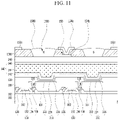
- FIG. 4 is a longitudinal-sectional view taken along line I-I' of FIG. 3
- FIG. 5 is a longitudinal-sectional view taken along line II-II' of FIG. 2 .
- a touch display device 1 senses changes in mutual capacitances Cm (touch sensors) by a user touch through touch electrodes 152e and 154e, and thus senses whether or not there is a touch and a touch position.
- Cm mutual capacitances
- the touch display device 1 having the touch sensors shown in FIG. 1 displays an image through unit pixels including light emitting devices 210.
- the unit pixel may include red (R), green (G) and blue (B) subpixels SP arranged in a row.
- the unit pixel may include red (R), green (G), blue (B) and white (W) subpixels SP.
- the unit pixel may be formed in a pentile structure. Referring to FIG. 3 , the unit pixel having the pentile structure may include one red (R) subpixel SP, one blue (B) subpixel SP and two green (G) subpixels SP.
- the touch display device 1 may include a plurality of subpixels SP arranged in a matrix on a substrate 111, an encapsulation unit 140 disposed on the subpixels SP, and the touch sensors Cm disposed on the encapsulation unit 140.
- Each of the subpixels SP include a pixel driving circuit, and the light emitting device 210 connected to the pixel driving circuit.
- the pixel driving circuit includes a switching transistor T1, a driving transistor T2 and a storage capacitor Cst.
- a switching transistor T1 a driving transistor T2
- a storage capacitor Cst a storage capacitor
- the present disclosure exemplarily describes the pixel driving circuit as having a structure including two transistors T and one capacitor C, the pixel driving circuit is not limited thereto.
- the pixel driving circuit having a 3T1C structure or a 3T2C structure including three or more transistors T and one or more capacitors C may be used.
- the switching transistor T1 is turned on, when a scan pulse is applied to a scan line SL, and supplies a data signal supplied to a data line DL to the storage capacitor Cst and a gate electrode of the driving transistor T2.
- the driving transistor T2 controls current I supplied from a high voltage (VDD) supply line to the light emitting device 210 in response to the data signal to the gate electrode of the corresponding driving transistor T2, thereby adjusting the amount of light emitted by the light emitting device 210. Further, even though the switching transistor T1 is turned off, the driving transistor T2 supplies regular current to the light emitting device 210 due to voltage charging the storage capacitor Cst so that the light emitting device 210 maintains light emission, until a data signal of the next frame is supplied to the driving transistor T2.
- VDD high voltage
- the driving thin film transistor 130 includes a semiconductor layer 134 disposed on a buffer layer 112, a gate electrode 132 configured to overlap the semiconductor layer 134 with a gate insulating film 102 interposed therebetween, and source and drain electrodes 136 and 138 formed on an interlayer insulating film 114 so as to contact the semiconductor layer 134.
- the semiconductor layer 134 may be formed of at least one of an amorphous semiconductor material, a polycrystalline semiconductor material or an oxide semiconductor material.
- the light emitting device 210 includes an anode 222, an emission stack 224 formed on the anode 222, and a cathode 226 formed on the emission stack 224.
- the anode may be conductively connected to the drain electrode 138 or the source electrode 136 of the driving thin film transistor 130 (T2) exposed through a pixel contact hole 116 formed through a pixel planarization layer 118.
- At least one emission stack 224 is formed on the anode 222 in an emission region prepared by a bank 128.
- the at least one emission stack 224 may be formed by stacking a hole-related layer, an emission layer and an electron-related layer on the anode 222 in regular order or in reverse order.
- the at least one emission stack 224 may include first and second emission stacks disposed opposite to each other with a charge generation layer interposed therebetween. In this case, one of the first and second emission stacks may emit blue light and the other of the first and second emission stacks may emit yellow-green light, and thereby the first and second emission stacks may produce white light.
- the white light produced by the emission stack 224 is incident upon a color filter located on the upper or lower surface of the emission stack 224, thereby being capable of implementing a color image.
- the respective emission stacks 224 of the light emitting devices 210 emit light with colors corresponding to the corresponding subpixels without separate color filters, thereby being capable of implementing a color image.
- the emission stack 224 of the red (R) subpixel SP may emit red light
- the emission stack 224 of the green (G) subpixel SP may emit green light
- the emission stack 224 of the blue (B) subpixel SP may emit blue light.
- the hole-related layer may include at least one of a hole injection layer and a hole transport layer.
- the electron-related layer may include at least one of an electron injection layer and an electron transport layer.
- the cathode 226 may be formed opposite the anode 222 with the emission stack 224 interposed therebetween.
- the cathode 226 may be connected to a low voltage (VSS) supply line.
- VSS low voltage
- the encapsulation unit 140 prevents external moisture or oxygen from permeating the light emitting devices 210 which are vulnerable to external moisture or oxygen.
- the encapsulation unit 140 includes a plurality of inorganic encapsulation layers 142 and 146 and an organic encapsulation layer 144 disposed between the inorganic encapsulation layers 142 and 146, and one of the inorganic encapsulation layers 142 and 146 is disposed as the uppermost layer.
- the encapsulation unit 140 includes at least two inorganic encapsulation layers 142 and 146 and at least one organic encapsulation layer 144.
- the structure of the encapsulation unit 140 in which an organic encapsulation layer 144 is disposed between first and second encapsulation layers 142 and 146 will be exemplarily described.
- the first inorganic encapsulation layer 142 may be formed on the substrate 111 provided with the cathode 226 formed thereon so as to be located closest to the light emitting devices 210.
- the first inorganic encapsulation layer 142 may be formed of an inorganic insulating material which may be deposited at a low temperature, such as silicon nitride (SiN x ), silicon oxide (SiO x ), silicon oxynitride (SiON) or aluminum oxide (Al 2 O 3 ). Further, the first inorganic encapsulation layer 142 may be formed of as a single layer structure or a multilayer structure.
- first inorganic encapsulation layer 142 is deposited at a low temperature, damage to the emission stacks 224 of the light emitting devices 210, which are vulnerable to high temperature, may be prevented during the deposition process of the first inorganic encapsulation layer 142.
- the organic encapsulation layer 144 serves as a buffer layer which relieves stress between respective layers caused by bending of the display device, and strengthens planarization performance.
- the organic encapsulation layer 144 is formed of an organic insulating material, such as an acrylic resin, an epoxy resin, polyimide, polyethylene or silicon oxycarbide (SiOC).
- At least one dam 106 may be disposed so as to prevent the organic encapsulation layer 144 in a liquid state from diffusing towards the edge of the substrate 111.
- the at least one dam 106 may prevent the organic encapsulation layer 144 from diffusing towards a pad area PDA, in which touch pads 170 and display pads 104 are disposed, at the outermost edge of the substrate 111.
- the at least one dam 106 may be formed to completely surround the active area AA in which the light emitting devices 210 are disposed.
- the at least one dam 106 is not limited thereto, the at least one dam 106 may be formed only between the active area AA and the pad area PDA.
- the pad area PDA in which the touch pads 170 and the display pads 104 are disposed, is disposed at one side of the substrate 111
- the at least one dam 106 may be disposed only at the corresponding side of the substrate 111.
- the pad area PDA in which the touch pads 170 and the display pads 104 are disposed, is disposed at both sides of the substrate 111
- the at least one dam 106 may be disposed at the two sides of the substrate 111.
- the at least one dam 106 is formed in a single layer structure or a multilayer structure.
- the at least one dam 106 may be formed of the same material at the same time as at least one of the pixel planarization layer 118, the bank 128 or spacers.
- the second inorganic encapsulation layer 146 may be formed on the substrate 111 provided with the organic encapsulation layer 144 formed thereon so as to the upper and side surfaces of the organic encapsulation layer 144 and the first inorganic encapsulation layer 142.
- the second inorganic encapsulation layer 146 may minimize or prevent permeation of external moisture or oxygen into the first inorganic encapsulation layer 142 and the organic encapsulation layer 144.
- the second inorganic encapsulation layer 146 may be formed of an inorganic insulating material, such as silicon nitride (SiN x ), silicon oxide (SiO x ), silicon oxynitride (SiON) or aluminum oxide (Al 2 O 3 ). Further, the second inorganic encapsulation layer 146 may be formed in a single layer structure or a multilayer structure.
- a touch buffer film 148 may be disposed on the encapsulation unit 140, and a black matrix 1000 may be disposed on the touch buffer film 148. Further, the touch sensors Cm including a first sensor layer 152 and a second sensor layer 154, which are disposed so as to intersect each other with the black matrix 1000 interposed therebetween, are disposed.
- the first sensor layer 152 may be a touch driving line
- the second sensor layer 154 may be a touch sensing line.
- the touch sensor Cm may be charged with electric charges due to a touch driving pulse supplied to the first sensor layer 152, and may discharge the electric charges to the second sensor layer 154.
- the first sensor layer 152 includes a plurality of first touch electrodes 152e, and first bridge electrodes 152b configured to conductively connect the first touch electrodes 152e.
- the first touch electrodes 152e may be disposed on the upper surface of the black matrix 100 so as to be spaced apart from each other by a designated interval in a first direction, i.e., an X-axis direction. Each of the first touch electrodes 152e may be conductively connected to adjacent first touch electrodes 152e by the first bridge electrodes 152b.
- the first bridge electrodes 152b are disposed on the same plane as the second touch electrodes 154e in the same plane on the black matrix 1000, and may be conductively connected to the second touch electrodes 154e without separate contact holes.
- the second sensor layer 154 includes a plurality of second touch electrodes 154e, and second bridge electrodes 154b configured to conductively connect the second touch electrodes 154e.
- the second touch electrodes 154e may be disposed on the black matrix 1000 so as to be spaced apart from each other by a designated interval in a second direction, i.e., a Y-axis direction. Each of the second touch electrodes 154e may be conductively connected to adjacent second touch electrodes 154e by the second bridge electrodes 154b.
- the second bridge electrodes 154b may be formed on the touch buffer film 148 formed of an insulating material, may be exposed through touch contact holes 150 formed through the black matrix 1000, and may be conductively connected to the second touch electrode 154e.
- the second bridge electrodes 154b may be disposed between the touch buffer film 148 and the black matrix 1000, and may be connected to the second touch electrodes 154e disposed on the black matrix 1000 through the touch contact holes 150 in the black matrix 1000.
- the first and second touch electrodes 152e and 154e and the first bridge electrodes 152b disposed on the upper surface of the black matrix 1000 may not overlap the emission regions of the respective subpixels SP, and may overlap the bank 128. Further, the first and second touch electrodes 152e and 154e and the first bridge electrodes 152b may be formed in a mesh type.
- the second bridge electrodes 154b disposed on the touch buffer film 148 may not overlap the emission regions of the respective subpixels SP, and may overlap the bank 128. Further, the second bridge electrodes 154b located between the touch buffer film 148 and the black matrix 1000 may be formed in a V-shape.
- the first and second touch electrodes 152e and 154e and the first and second bridge electrodes 152b and 154b are disposed so as not to overlap the emission regions of the respective subpixels SP, and thus, deterioration of the aperture ratio and transmittance of the touch display device 1 due to the first and second touch electrodes 152e and 154e and the first and second bridge electrodes 152b and 154b may be prevented.
- openings 1550 may be formed through the black matrix 1000.
- the openings 1550 are disposed so as to overlap the emission regions of the respective subpixels SP, i.e., to correspond to regions in which the light emitting devices 210 are disposed.
- the openings 1550 may be formed to expose some parts of the upper surface of the touch buffer film 148 disposed under the black matrix 1000 by removing some regions of the black matrix 1000. Therefore, the openings 1550 formed by removing the black matrix 1000 may serve as the upper surface of the touch buffer film 148 and the side surface of the black matrix 1000. Therefore, each of the openings 1550 may include a lower surface formed of the exposed upper surface of the touch buffer film 148, and a side surface formed of the exposed side surface of the black matrix 1000.
- Color filters 1500 may be disposed in the opening 1550. Therefore, the black matrix 1000 may be disposed between the color filters 1500 so as to overlap the bank 128.
- the black matrix 100 may divide respective subpixel regions from each other and serve to prevent optical interference and light leakage between adjacent subpixel regions.
- the black matrix 1000 may be formed of a black insulating material having high resistance.
- the openings 1550 and the color filters 1500 disposed in the openings 1550 may be designed to have a width equal to or greater than the width of the emission regions exposed from the bank 128.
- the emission regions may be defined as regions in which the lower surface of the emission stack 224 directly contacts the upper surface of the anode 222 by removing the bank 128 disposed on the anode 222.
- the color filters 1500 disposed in the openings 1550 may be formed using an inkjet printing method, or may be formed through a photolithography process. This figure illustrates the color filters 1500 as being formed by injecting color inks using the inkjet printing method and then hardening the color inks.
- the color filters 1500 may be formed on some parts of the upper surface of the buffer film 148 exposed through the openings 1550 and some parts of the side surface of the black matrix 1000 exposed through the openings 1550.
- the color inks of the color filters 1500 used to fill the openings 1550 using the inkjet printing method may overflow the openings 1550 and flow to adjacent subpixels configured to emit light with different colors.
- the touch buffer film 148 may be formed of a hydrophilic material, i.e., a material which has strong affinity for the color inks of the color filters 1500, and the black matrix 1000 may be formed of a hydrophobic material, i.e., a material which repels the color inks.
- repulsive force may be generated between the color filters 1500 and the hydrophobic black matrix 1000, and attractive force may be generated between the color filters 1500 and the hydrophilic touch buffer film 148. Therefore, even though the applied thickness of the black matrix 1000, i.e., the height of the black matrix 1000, is low, overflow of the color inks of the color filters 1500 to adjacent subpixels configured to emit light with different colors may be prevented.
- the color inks of the color filters 1500 repel the material of the black matrix 1000, the color inks have repulsive force with respect to the black matrix 1000, and is thus formed in a convex shape.
- the color filters 1500 may be formed in a convex shape based on the upper surface of the black matrix 1000.
- the touch display device 1 may include the active area AA in which the light emitting devices 210 are disposed, and a bezel area BZ disposed adjacent to the active area AA.
- the bezel area BZ may include a first bezel area BZ1 disposed adjacent to the active area AA, the pad area PDA in which the touch pads 170 are disposed, and a second bezel area BZ2 disposed between the first bezel area BZ1 and the pad area PDA.
- the dam 106 disposed adjacent to the organic encapsulation layer 144 of the encapsulation unit 140 may be formed in the first bezel area BZ1.
- the display pads 104 may also be disposed.
- the display pads 104 may be disposed between the touch pads 170.
- the touch pads 170 may be disposed between the display pads 104.
- both touch pads 170 and the display pads 104 are disposed at one side of the display panel, the touch pads 170 and the display pads 104 are not limited thereto.
- the touch pads 170 may be disposed at one side of the display panel, and the display pads 104 may be disposed at the other side of the display panel. Therefore, the disposition of the touch pads 170 and the display pads 104 are not limited to the structure of FIG. 2 , and may be variously changed depending on the design of the touch display device 1.
- the display pads 104 are formed to have the same stack structure as the touch pads 170. However, the display pads 104 are not limited thereto, and may be formed to have a different stack structure from the touch pads 170.
- the touch display device 1 includes routing lines 160 disposed in the bezel area BZ.
- the routing lines 160 transmit a touch driving signal generated by a touch driver to the first sensor layer 152 through the touch pads 170, and transmit a touch signal from the second sensor layer 154 to the touch driver through the touch pads 170.
- the routing lines 160 may be formed between each of the first and second touch electrodes 152e and 154e and the touch pads 170. Further, the routing lines 160 may conductively connect each of the first and second touch electrodes 152e and 154e and the touch pads 170. As shown in FIG. 2 , the routing lines 160 may extend from the second touch electrodes 154e to at least one of left or right sides of the active area AA, and may be connected to the touch pads 170 in the pad area PDA. The routing lines 160 may extend from the first touch electrodes 152e to at least one of upper and lower sides of the active area AA, and may be connected to the touch pads 170. Such disposition of the routing lines may be variously changed according to the design of the touch display device 1.
- the routing lines 160 may be disposed on at least one dam 106 so as to intersect the at least one dam 106, and may be disposed along the side surface of the encapsulation unit 140. Therefore, the routing lines 160 may overlap the upper surface of the at least one dam 106.
- the routing lines 160 and the first and second touch electrodes 152e and 154e may be selectively formed on the same plane.
- the routing lines 160 may be disposed on the black matrix 1000 in the active area AA, the first bezel area BZ1 and the second bezel area BZ2.
- routing lines 160 are not limited thereto, and the routing lines 160 and the first and second touch electrodes 152e and 154e may be disposed on different planes.
- the routing lines 160 may be disposed on the black matrix 1000 in the first bezel area BZ1 and the active area AA.
- the routing lines 160 may be disposed on the touch buffer film 148 in the second bezel area BZ2.
- FIG. 5 illustrates the case in which the routing lines 160 are disposed on the touch buffer film 148 in the second bezel area BZ2, and are disposed on the black matrix 1000 in the first bezel area BZ1 and the active area AA.
- the routing lines 160 are disposed on the black matrix 1000 in the first bezel area BZ1 and the active area AA, and are disposed on the touch buffer film 148 in the second bezel area BZ2 will be described in more detail.
- the black matrix 1000 may be disposed in the active area AA and the first bezel area BZ1, but may not be disposed in some regions of the second bezel area BZ2. Therefore, in the second bezel area BZ2 among the bezel area BZ, the routing lines 160 may contact the upper surface of the touch buffer film 148.
- the first and second touch electrodes 152e and 154e and the routing lines 160 may be disposed on the black matrix 1000 in the active area AA and the first bezel area BZ1.
- the openings 1550 and the touch contact holes 150 may be formed in the black matrix 1000, thereby being capable of exposing some parts of the touch buffer film 148, disposed under the black matrix 1000, and the second bridge electrodes 154b.
- openings 1550 and the touch contact holes 150 are formed by removing some regions of the black matrix 1000 disposed in the active area AA, some regions of the black matrix 1000 disposed in the bezel area BZ may be removed.
- the black matrix 1000 disposed in the second bezel area BZ2 and the pad area PDA among the bezel area BZ may be selectively removed.
- the black matrix 1000 may be removed from the bending region of the second bezel area BZ2.
- at least a part of the black matrix 1000 may be removed.
- the routing lines 160 and the first and second touch electrodes 152e and 154e may be disposed on different layers.
- the third touch pad electrodes 176 formed of the same material to have the same stack structure as the routing lines 160 may be disposed on different layers from the first and second touch electrodes 152e and 154e.
- the first and second touch electrodes 152e and 154e and some parts of the routing lines 160 may be disposed on the black matrix 1000 in the first bezel area BZ1.
- the routing lines 160 may be disposed on the touch buffer film 148 in the second bezel area BZ2.
- the third touch pad electrodes 176 having the same stack structure as the routing lines 160 may be disposed on the second touch pad electrodes 174 in the pad area PDA.
- the routing lines 160 are disposed on the black matrix 1000 in the active area AA, the first bezel area BZ1 and the second bezel area BZ2, in the same manner as the first and second touch electrodes 152e and 154e disposed on the black matrix 1000 in the active area AA, will be described.
- the black matrix 1000 may be disposed in the first bezel area BZ1, the second bezel area BZ2 and the pad area PDA among the bezel area BZ.
- some regions of the black matrix 1000 may be removed.
- the first and second touch electrodes 152e and 154e and the routing lines 160 may be formed on the same layer, i.e., the black matrix 1000, in the first bezel area BZ1 and the second bezel area BZ2. Further, the third touch pad electrodes 176 may be disposed on the second touch pad electrodes 174 exposed through the first pad contact holes 178a in the pad area PDA.
- the black matrix 1000 disposed on the second touch pad electrodes 174 and the touch buffer film 148 in the bezel area BZ may be selectively removed.
- each of the first sensor layer 152 and the second sensor layer 154 may be conductively connected to the touch driver (not shown) through the routing lines 160 and the touch pads 170.
- the touch pads 170 may be connected to a signal transfer film (not shown) on which the touch driver is mounted.
- Each of the touch pads 170 disposed in the pad area PDA may include the first to third touch pad electrodes 172, 174 and 176.
- the first touch pad electrode 172 may be disposed on at least one of the substrate 111, the buffer layer 112 or the interlayer insulating film 114 which is disposed below the encapsulation unit 140.
- the first touch pad electrode 172 may be formed of the same material on the same plane as at least one of the gate electrode 132 or the source and drain electrodes 136 and 138 of the driving transistor 130 (T2), and may be formed in a single layer structure or a multilayer structure.
- the first touch pad electrode 172 may have the same stack structure as at least one of the gate electrode 132 or the source and drain electrodes 136 and 138.
- the first touch pad electrode 172 which is formed of the same material as the source and drain electrodes 136 and 138 and disposed on the interlayer insulating film 114, is illustrated. Therefore, the first touch pad electrode 172 may be formed through the same mask process as the source and drain electrodes 136 and 138. Therefore, the first touch pad electrode 172 may have the same stack structure as the source and drain electrodes 136 and 138.
- the second touch pad electrode 174 may be conductively connected to the first touch pad electrode 172 exposed through the first pad contact hole 178a formed through the touch buffer film 148.
- the second touch pad electrode 174 may be formed through the same mask process as the second bridge electrodes 154b, thus being capable of being formed of the same material on the same plane as the second bridge electrodes 154b. Further, the second touch pad electrode 174 may have the same stack structure as the second bridge electrodes 154b.
- the third touch pad electrode 176 may be conductively connected to the second touch pad electrode 174 exposed from the black matrix 1000.
- the third touch pad electrode 176 may be formed through the same mask process as the first and second touch electrodes 152e and 154e. Therefore, the third touch pad electrode 176 may be formed of the same material as the first and second touch electrodes 152e and 154e. Further, the third touch pad electrode 176 may have the same stack structure as the first and second touch electrodes 152e and 154e. Therefore, the third touch pad electrode 176 may have the same stack structure as the routing lines 160 respectively extending from the first and second touch electrodes 152e and 154e. The third touch pad electrode 176 may extend from each of the routing lines 160.
- a cover layer 500 may be disposed on the substrate 111 provided with the encapsulation unit 140 and the touch sensors Cm disposed thereon.
- the cover layer 500 may include a passivation layer 520, a black optical adhesive layer 550 disposed on the passivation layer 520, and a cover window 590 disposed on the black optical adhesive layer 550.
- the passivation layer 520 and the black optical adhesive layer 550 and the cover window 590 may be disposed up to the first bezel area BZ1.
- the passivation layer 520 and the black optical adhesive layer 550 and the cover window 590 are not limited thereto, and may be disposed up to the second bezel area BZ2.
- the black optical adhesive layer 550 may serve as both an adhesive layer and a polarization layer.
- the polarization layer serves to block light reflected by metals forming the touch electrodes 152 and 154.
- the black optical adhesive layer 550 may prevent reflection of external light and prevent color interference between the subpixels.
- the black matrix 100 may block light reflected by the metals forming the touch electrodes 152 and 154, and thus, the touch display device 1 according to one embodiment of the present disclosure may display a clearer image.
- the black optical adhesive layer 550 may be implemented in black using a material in which a dye is combined with an adhesive sheet, such as an optically clear adhesive (OCA), so as to serve as both an adhesive layer and a polarization layer in a black color tone.
- OCA optically clear adhesive
- the lower surface of the passivation layer 520 may have an uneven surface due to the touch electrodes 152 and 154 and the color filters 1500 disposed under the passivation layer 520.
- the upper surface of the passivation layer 520 may have a flat surface.
- the passivation layer 520 may be formed of an organic material having fluidity.
- the passivation layer 520 may be formed of an organic material, such as an acrylic resin, an epoxy resin, polyimide, polyethylene or silicon oxycarbide (SiOC).
- the touch display device 1 may replace a touch insulating film with the black matrix 1000 and embed the color filters 1500 in the black matrix 1000, thereby being capable simplifying the structure of the touch display device 1 and the manufacturing process thereof.
- the touch display device 1 may replace the touch insulating film with the black matrix 1000 and embed color filters 1500 in the black matrix 1000 so as to realize slimness of the touch display panel, and may use the black optical adhesive layer 550 as a substitute for a polarization plate because the black optical adhesive layer 550 applied together with the black matrix 1000 may reduce reflectance.
- FIG. 6 is a longitudinal-sectional view of a touch display device according to another embodiment of the present disclosure
- FIG. 7 is a longitudinal-sectional view of a touch display device according to yet another embodiment of the present disclosure.
- FIGs. 6 and 7 A detailed description of some parts in these embodiments shown in FIGs. 6 and 7 , which are substantially the same as those in the former embodiment shown in FIGs. 1 to 5 , will be omitted because it is considered to be unnecessary, and FIGs. 1 to 5 will be cited for ease of description.
- a touch display device 2 includes a first optical adhesive layer 523 disposed on a black matrix 1000, a polarization layer 530 disposed on the first optical adhesive layer 523, a second optical adhesive layer 525 disposed on the polarization layer 530, and a cover window layer 590 disposed on the second optical adhesive layer 525.
- the polarization layer 530 may be used to block light reflected by metals forming touch electrodes 152 and 154.
- the first optical adhesive layer 523 may be disposed between a lower layer including the black matrix 1000 and the polarization layer 530, and may serve to adhere the black matrix 1000 and the polarization layer 530 to each other.
- the polarization layer 530 may be formed by applying a polarizing material to the black matrix 1000, or may be formed as a separate component. Therefore, the polarization layer 530 may be adhered to the black matrix 1000 by interposing a layer, which may adhere the lower layer including the black matrix 1000 and the polarization layer 530 to each other, therebetween.
- the polarization layer 530 may employ polyvinyl alcohol (PVA), triacetyl cellulose (TAC) or the like.
- the second optical adhesive layer 525 may exhibit the same function as the first optical adhesive layer 523.
- the first and second optical adhesive layers 523 and 525 may employ an optically clear adhesive (OCA).
- a touch display device 3 includes a passivation layer 510 disposed on a black matrix 1000, a first optical adhesive layer 523 disposed on the passivation layer 510, a polarization layer 530 disposed on the first optical adhesive layer 523, a second optical adhesive layer 525 disposed on the polarization layer 530, and a cover window layer 590 disposed on the second optical adhesive layer 525.
- the polarization layer 530 may be used to block light reflected by metals forming touch electrodes 152 and 154.
- the passivation layer 510 may protect the black matrix 1000, color filters 1500 and the touch electrodes 152 and 154 disposed under the passivation layer 510 from external moisture, oxygen and foreign substances.
- the touch display devices 2 and 3 may realize slimness of a touch display panel, may reduce reflectance through use of the polarization layer 530, and protect structures located under the passivation layer 510 from foreign substances.
- FIGs. 8 to 12 are longitudinal-sectional views illustrating a method for manufacturing the touch display device according to one embodiment of the present disclosure.
- FIGs. 8 to 12 A detailed description of some parts of the method shown in FIGs. 8 to 12 , which are substantially the same as those in the embodiment shown in FIGs. 1 to 5 , will be omitted because it is considered to be unnecessary, and FIGs. 1 to 5 will be cited for ease of description.
- a first touch metal layer is deposited onto the entire surface of the substrate 111 provided with the encapsulation unit 140 and the touch buffer film 148 formed thereon.
- the second bridge electrodes 154b and the second touch pad electrodes 174 may be formed by patterning the first touch metal layer through a mask process.
- the first touch metal layer is formed to have a single layer structure or a multilayer structure using a metal, such as aluminum (Al), titanium (Ti), copper (Cu), molybdenum (Mo), tantalum (Ta) or molybdenum-titanium (MoTi).
- a metal such as aluminum (Al), titanium (Ti), copper (Cu), molybdenum (Mo), tantalum (Ta) or molybdenum-titanium (MoTi).
- the first touch metal layer may be formed to have a three-layer stack structure, such as titanium/aluminum/titanium (Ti/Al/Ti), molybdenum-titanium/copper/molybdenum-titanium (MoTi/Cu/MoTi) or titanium/aluminum/molybdenum (Ti/Al/Mo).
- a matrix material is deposited onto the entire surface of the substrate 111 provided with the second bridge electrodes 154b and the second touch pad electrodes 174 formed thereon.
- the black matrix 100 and the touch contact holes 150, and the openings 1550 and second pad contact holes 178b formed therein may be formed by patterning the black matrix material through a mask process.
- the touch contact holes 150 may be disposed at positions, each of which corresponds to a part of a corresponding one of the second bridge electrodes 154b, and second pad contact holes 178b may be disposed at positions corresponding to the first touch pad electrodes 172. Further, the openings 1550 may be formed at positions corresponding to the anodes 222.
- the second bridge electrodes 154b and the second touch pad electrodes 174 may be protected. That is to say, because the second bridge electrodes 154b and the second touch pad electrodes 174 do not react to a chemical solution (for example, a developer) used during the manufacturing process of the black matrix 1000, corrosion of the second bridge electrodes 154b and the second touch pad electrodes 174 may be prevented.
- a chemical solution for example, a developer
- the color filters 1500 may be formed by injecting color inks into the openings 1550 using the inkjet printing method and hardening the color inks.
- the black matrix 1000 may be formed of a hydrophobic material, i.e., a material which repels the color inks
- the color filters 1500 may be formed in a convex shape based on the upper surface of the black matrix 1000.
- the color filters 1500 are formed in the openings 1550 formed in the black matrix 1000 using the inkjet printing method, and thus, the manufacturing process of the touch display device may be simplified.
- a second touch metal layer is deposited onto the entire surface of the substrate 111 provided with the color filters 1500 filling the openings 1550 and the touch contact holes 150 configured to open the second bridge electrodes 154b, and is then patterned through a mask process.
- the first and second touch electrodes 152e and 154e, the first bridge electrodes 152b, the routing lines 160 and the third touch pad electrodes 176 may be formed by patterning the second touch metal layer.
- the second touch metal layer is formed to have a single layer structure or a multilayer structure using a metal, such as aluminum (Al), titanium (Ti), copper (Cu), molybdenum (Mo), tantalum (Ta) or molybdenum-titanium (MoTi).
- a metal such as aluminum (Al), titanium (Ti), copper (Cu), molybdenum (Mo), tantalum (Ta) or molybdenum-titanium (MoTi).
- the second touch metal layer may be formed to have a three-layer stack structure, such as titanium/aluminum/titanium (Ti/Al/Ti), molybdenum-titanium/copper/molybdenum-titanium (MoTi/Cu/MoTi) or titanium/aluminum/molybdenum (Ti/Al/Mo).
- the cover layer 500 may be formed on the substrate 111 provided with the first and second touch electrodes 152e and 154e and the first bridge electrodes 152b formed thereon.
- the cover layer 500 may include the cover window 590.
- the black optical adhesive layer 550 may be further disposed between the cover window 590 and the substrate 111 provided with the first and second touch electrodes 152e and 154e and the first bridge electrodes 152b formed thereon.
- the passivation layer 510 may be formed on the substrate 111 provided with the first and second touch electrodes 152e and 154e and the first bridge electrodes 152b formed thereon, and may be adhered to the cover window 590 by an optical adhesive layer disposed on the passivation layer 510.
- FIGs. 13 and 14 are longitudinal-sectional views of a touch display device according to still another embodiment of the present disclosure.
- FIG. 13 illustrates the structure of an active area of the touch display device according to still another embodiment of the present disclosure
- FIG. 14 illustrates the structure of a bezel area of the touch display device according to still another embodiment of the present disclosure.
- FIGs. 13 and 14 A detailed description of some parts in this embodiment shown in FIGs. 13 and 14 , which are substantially the same as those in the former embodiment shown in FIGs. 1 to 5 , will be omitted because it is considered to be unnecessary, and FIGs. 1 to 5 will be cited for ease of description.
- color filters 1600 may be formed in a different shape from the color filters 1500 of the touch display device 1 according to one embodiment of the present disclosure.
- the color filters 1500 may be formed using the inkjet printing method, and may thus have a convex shape based on the upper surface of the black matrix 1000.
- the color filters 1600 may be formed using a photomask process, and may thus be formed in a protruding shape from the upper surface of the black matrix 1000.
- openings 1550 may be formed to have a tapered shape in the downward direction of the black matrix 1000.
- the black matrix 1000 is formed of an opaque material and thus absorbs light during a light exposure process, and thus it may be difficult to allow light to reach the touch buffer film 148 disposed under the black matrix 1000.
- the material of the color filters 1600 may not be hardened. Therefore, the upper portion of each of the openings 1550 may be greater in size than the lower portion of each of the openings 1550 so that light may reach the touch buffer film 148 disposed under the color filter 1600.
- the material of the color filters 1600 may require a greater amount than the amount to fill the openings 1550 of the black matrix 100 for forming the application thickness.
- the color filters 1550 formed by hardening the organic material may have a flat upper surface while filling the openings 1550.
- a greater amount of the material of the color filters 1600 than the amount to fill the openings 1550 must be provided to the substrate 111.
- the color filters 1600 may have a protruding surface from the upper surface of the black matrix 1000 so as to form a step with the upper surface of the black matrix 1000. That is to say, the color filters 1600 may be formed to protrude from the upper portions of the corresponding openings 1550.
- the black matrix 1000 may be disposed on the touch buffer film 148.
- the black matrix 1000 may be selectively disposed on the touch buffer film 148 in the bezel area BZ.
- the black matrix 1000 is removed from the first bezel area BZ1 and the pad area PDA of the bezel area BZ.
- the black matrix 1000 may be formed to be left in the bezel area BZ while touch contact holes 150 and the openings 1550 are formed through the black matrix 1000. Therefore, this embodiment describes that the black matrix 1000 may be disposed on the entire surfaces of the bezel area BZ.
- second touch pad contact holes 178b may be further formed through the black matrix 1000 in the pad area PDA, and third touch pad electrodes 176 having the same stack structure as routing lines 160 may be disposed in the second touch pad contact holes 178b.
- a touch display device may replace a touch insulating film with a black matrix and embed color filters in the black matrix, thereby being capable of simplifying the structure of the touch display device and the manufacturing process thereof.
- the touch display device may replace the touch insulating film with the black matrix and embed the color filters in the black matrix so as to realize slimness of a touch display panel, and may use a black optical adhesive layer, applied together with the black matrix, as a substitute for a polarization plate so as to reduce reflectance.
Landscapes
- Engineering & Computer Science (AREA)
- General Engineering & Computer Science (AREA)
- Theoretical Computer Science (AREA)
- Physics & Mathematics (AREA)
- Human Computer Interaction (AREA)
- General Physics & Mathematics (AREA)
- Optics & Photonics (AREA)
- Devices For Indicating Variable Information By Combining Individual Elements (AREA)
- Electroluminescent Light Sources (AREA)
- Push-Button Switches (AREA)
- Electrophonic Musical Instruments (AREA)
- Fittings On The Vehicle Exterior For Carrying Loads, And Devices For Holding Or Mounting Articles (AREA)
Applications Claiming Priority (1)
| Application Number | Priority Date | Filing Date | Title |
|---|---|---|---|
| KR1020200190018A KR20220097048A (ko) | 2020-12-31 | 2020-12-31 | 터치 디스플레이 장치 |
Publications (1)
| Publication Number | Publication Date |
|---|---|
| EP4024180A1 true EP4024180A1 (en) | 2022-07-06 |
Family
ID=78957663
Family Applications (1)
| Application Number | Title | Priority Date | Filing Date |
|---|---|---|---|
| EP21215976.8A Pending EP4024180A1 (en) | 2020-12-31 | 2021-12-20 | Touch display device |
Country Status (6)
| Country | Link |
|---|---|
| US (1) | US11635835B2 (ja) |
| EP (1) | EP4024180A1 (ja) |
| JP (1) | JP7304400B2 (ja) |
| KR (1) | KR20220097048A (ja) |
| CN (1) | CN114690946A (ja) |
| TW (1) | TWI820548B (ja) |
Families Citing this family (1)
| Publication number | Priority date | Publication date | Assignee | Title |
|---|---|---|---|---|
| WO2023184306A1 (zh) * | 2022-03-31 | 2023-10-05 | 京东方科技集团股份有限公司 | 触控显示面板和触控显示装置 |
Citations (5)
| Publication number | Priority date | Publication date | Assignee | Title |
|---|---|---|---|---|
| KR20140143498A (ko) * | 2013-06-07 | 2014-12-17 | 전자부품연구원 | 블랙매트릭스를 이용한 대면적 터치센서 제조방법 |
| US20180032193A1 (en) * | 2016-07-29 | 2018-02-01 | Boe Technology Group Co., Ltd. | Touch panel and manufacturing method thereof, display apparatus having the same |
| EP3301553A1 (en) * | 2016-09-30 | 2018-04-04 | LG Display Co., Ltd. | Display device with touch sensor |
| US20190064960A1 (en) * | 2017-08-28 | 2019-02-28 | Samsung Display Co., Ltd. | Display device |
| US20190187850A1 (en) * | 2017-12-14 | 2019-06-20 | Lg Display Co., Ltd. | Display apparatus with integrated touch screen |
Family Cites Families (18)
| Publication number | Priority date | Publication date | Assignee | Title |
|---|---|---|---|---|
| JP2002148429A (ja) | 2000-11-16 | 2002-05-22 | Canon Inc | 光学素子とその製造方法、該光学素子を用いた液晶素子 |
| JP2009198904A (ja) | 2008-02-22 | 2009-09-03 | Mitsubishi Chemicals Corp | 着色樹脂組成物、カラーフィルタおよび液晶表示装置 |
| KR101552994B1 (ko) | 2012-08-31 | 2015-09-15 | 엘지디스플레이 주식회사 | 유기 발광 표시 장치 및 이의 제조 방법 |
| KR102124906B1 (ko) * | 2013-12-26 | 2020-07-07 | 엘지디스플레이 주식회사 | 터치스크린을 구비한 유기전계 발광소자 및 이의 제조 방법 |
| KR20160128513A (ko) * | 2015-04-28 | 2016-11-08 | 삼성디스플레이 주식회사 | 터치 센서를 포함하는 표시 장치 |
| KR102146271B1 (ko) * | 2015-06-03 | 2020-08-21 | 동우 화인켐 주식회사 | 플렉서블 컬러필터와 그를 포함하는 플렉서블 유기 발광 표시 장치 및 그 제조방법 |
| KR101750428B1 (ko) | 2015-09-24 | 2017-06-23 | 엘지디스플레이 주식회사 | 터치 스크린 일체형 표시장치 |
| KR101908982B1 (ko) * | 2016-08-31 | 2018-10-17 | 엘지디스플레이 주식회사 | 터치 센서를 가지는 유기 발광 표시 장치 및 그 제조 방법 |
| KR102089340B1 (ko) | 2016-08-31 | 2020-03-16 | 엘지디스플레이 주식회사 | 터치 센서를 가지는 유기 발광 표시 장치 및 그 제조 방법 |
| KR102608954B1 (ko) * | 2016-09-30 | 2023-12-05 | 삼성디스플레이 주식회사 | 표시 장치 |
| KR102662681B1 (ko) | 2016-12-26 | 2024-04-30 | 엘지디스플레이 주식회사 | 터치 스크린 일체형 표시장치와 그의 제조방법 |
| KR20180076689A (ko) | 2016-12-28 | 2018-07-06 | 엘지디스플레이 주식회사 | 표시 장치 |
| CN107275512A (zh) * | 2017-05-25 | 2017-10-20 | 厦门天马微电子有限公司 | 一种有机电致发光显示面板、其制作方法及显示装置 |
| KR102390478B1 (ko) * | 2017-10-31 | 2022-04-25 | 엘지디스플레이 주식회사 | 터치 센서를 가지는 표시 장치 |
| KR102514873B1 (ko) * | 2017-11-29 | 2023-03-29 | 삼성전자주식회사 | 엘이디 디스플레이 장치 |
| KR102655476B1 (ko) | 2018-05-03 | 2024-04-08 | 삼성디스플레이 주식회사 | 유기발광 표시장치 |
| KR102664311B1 (ko) * | 2018-11-14 | 2024-05-09 | 엘지디스플레이 주식회사 | 표시 장치 |
| KR20200145887A (ko) * | 2019-06-19 | 2020-12-31 | 삼성디스플레이 주식회사 | 표시 장치 및 이를 포함하는 표시 장치의 제조 방법 |
-
2020
- 2020-12-31 KR KR1020200190018A patent/KR20220097048A/ko active Search and Examination
-
2021
- 2021-12-16 US US17/553,204 patent/US11635835B2/en active Active
- 2021-12-20 JP JP2021205923A patent/JP7304400B2/ja active Active
- 2021-12-20 EP EP21215976.8A patent/EP4024180A1/en active Pending
- 2021-12-22 CN CN202111582222.5A patent/CN114690946A/zh active Pending
- 2021-12-24 TW TW110148600A patent/TWI820548B/zh active
Patent Citations (5)
| Publication number | Priority date | Publication date | Assignee | Title |
|---|---|---|---|---|
| KR20140143498A (ko) * | 2013-06-07 | 2014-12-17 | 전자부품연구원 | 블랙매트릭스를 이용한 대면적 터치센서 제조방법 |
| US20180032193A1 (en) * | 2016-07-29 | 2018-02-01 | Boe Technology Group Co., Ltd. | Touch panel and manufacturing method thereof, display apparatus having the same |
| EP3301553A1 (en) * | 2016-09-30 | 2018-04-04 | LG Display Co., Ltd. | Display device with touch sensor |
| US20190064960A1 (en) * | 2017-08-28 | 2019-02-28 | Samsung Display Co., Ltd. | Display device |
| US20190187850A1 (en) * | 2017-12-14 | 2019-06-20 | Lg Display Co., Ltd. | Display apparatus with integrated touch screen |
Also Published As
| Publication number | Publication date |
|---|---|
| CN114690946A (zh) | 2022-07-01 |
| US20220206617A1 (en) | 2022-06-30 |
| JP2022105283A (ja) | 2022-07-13 |
| JP7304400B2 (ja) | 2023-07-06 |
| US11635835B2 (en) | 2023-04-25 |
| TW202227884A (zh) | 2022-07-16 |
| TWI820548B (zh) | 2023-11-01 |
| KR20220097048A (ko) | 2022-07-07 |
Similar Documents
| Publication | Publication Date | Title |
|---|---|---|
| US11744134B2 (en) | Organic light emitting display having touch sensor and method of fabricating the same | |
| US11301100B2 (en) | Display device | |
| US10490610B2 (en) | Display device | |
| CN108241451B (zh) | 显示装置 | |
| US11610946B2 (en) | Display device | |
| US11462597B2 (en) | Organic light-emitting display device having touch sensor | |
| US11256356B2 (en) | Display device having touch sensor and black matrix on the encapsulation unit | |
| CN108958529B (zh) | 显示装置及其制造方法 | |
| CN111180486A (zh) | 显示装置 | |
| US20210175476A1 (en) | Touch display device | |
| US11226695B2 (en) | Display device | |
| US11943967B2 (en) | Display panel and display device comprising the same | |
| CN111190498B (zh) | 显示装置 | |
| EP4024180A1 (en) | Touch display device | |
| KR102009330B1 (ko) | 유기 발광 표시 장치 |
Legal Events
| Date | Code | Title | Description |
|---|---|---|---|
| PUAI | Public reference made under article 153(3) epc to a published international application that has entered the european phase |
Free format text: ORIGINAL CODE: 0009012 |
|
| STAA | Information on the status of an ep patent application or granted ep patent |
Free format text: STATUS: REQUEST FOR EXAMINATION WAS MADE |
|
| 17P | Request for examination filed |
Effective date: 20211220 |
|
| AK | Designated contracting states |
Kind code of ref document: A1 Designated state(s): AL AT BE BG CH CY CZ DE DK EE ES FI FR GB GR HR HU IE IS IT LI LT LU LV MC MK MT NL NO PL PT RO RS SE SI SK SM TR |
|
| RBV | Designated contracting states (corrected) |
Designated state(s): AL AT BE BG CH CY CZ DE DK EE ES FI FR GB GR HR HU IE IS IT LI LT LU LV MC MK MT NL NO PL PT RO RS SE SI SK SM TR |
|
| STAA | Information on the status of an ep patent application or granted ep patent |
Free format text: STATUS: EXAMINATION IS IN PROGRESS |
|
| 17Q | First examination report despatched |
Effective date: 20230504 |