EP4022364B1 - Optische vorrichtung - Google Patents
Optische vorrichtung Download PDFInfo
- Publication number
- EP4022364B1 EP4022364B1 EP20808492.1A EP20808492A EP4022364B1 EP 4022364 B1 EP4022364 B1 EP 4022364B1 EP 20808492 A EP20808492 A EP 20808492A EP 4022364 B1 EP4022364 B1 EP 4022364B1
- Authority
- EP
- European Patent Office
- Prior art keywords
- substrate
- cavities
- coating layer
- transmission
- une
- Prior art date
- Legal status (The legal status is an assumption and is not a legal conclusion. Google has not performed a legal analysis and makes no representation as to the accuracy of the status listed.)
- Active
Links
Images


Classifications
-
- G—PHYSICS
- G02—OPTICS
- G02B—OPTICAL ELEMENTS, SYSTEMS OR APPARATUS
- G02B1/00—Optical elements characterised by the material of which they are made; Optical coatings for optical elements
- G02B1/10—Optical coatings produced by application to, or surface treatment of, optical elements
- G02B1/11—Anti-reflection coatings
- G02B1/118—Anti-reflection coatings having sub-optical wavelength surface structures designed to provide an enhanced transmittance, e.g. moth-eye structures
-
- G—PHYSICS
- G02—OPTICS
- G02B—OPTICAL ELEMENTS, SYSTEMS OR APPARATUS
- G02B1/00—Optical elements characterised by the material of which they are made; Optical coatings for optical elements
- G02B1/10—Optical coatings produced by application to, or surface treatment of, optical elements
- G02B1/12—Optical coatings produced by application to, or surface treatment of, optical elements by surface treatment, e.g. by irradiation
-
- G—PHYSICS
- G02—OPTICS
- G02B—OPTICAL ELEMENTS, SYSTEMS OR APPARATUS
- G02B5/00—Optical elements other than lenses
- G02B5/08—Mirrors
- G02B5/0808—Mirrors having a single reflecting layer
-
- G—PHYSICS
- G02—OPTICS
- G02B—OPTICAL ELEMENTS, SYSTEMS OR APPARATUS
- G02B5/00—Optical elements other than lenses
- G02B5/20—Filters
- G02B5/208—Filters for use with infrared or ultraviolet radiation, e.g. for separating visible light from infrared and/or ultraviolet radiation
Definitions
- the present invention relates to an optical device, suitable for the transmission or reflection of radiation in a predetermined wavelength range, for example of the ultraviolet, visible, infrared or microwave type.
- the field of the invention is that of optical devices, designed for example to equip imaging systems.
- the applications depend on the wavelength range.
- anti-reflective or mirror effects can be obtained by multi-layer construction and/or by structuring optical devices.
- the aim of the present invention is to propose an optical device, of the anti-reflective or mirror type, having improved properties.
- the invention relates to an optical device according to claim 1.
- the invention makes it possible to modify the front of an electromagnetic wave in a controlled manner.
- Texturing allows to vary the effective refractive index on the surface of the textured device. In particular, texturing allows to obtain lower effective refractive indices in a controlled manner, in the textured coating layer and in the textured area of the substrate. Texturing allows to obtain effective indices unattainable directly using multilayers. The indices are variable depending on the wavelength of the radiation.
- the invention makes it possible to increase the range of incidence angle for which the validity of the optical function is interesting.
- the device structure forms at least one bi-layer system, comprising the textured coating layer and the textured substrate layer, overlying the non-textured portion of the substrate.
- the optical device has an anti-reflective function.
- the invention makes it possible to improve the transmission of the device, in terms of spectral width and maximum transmission (therefore minimum absorption), compared to an untextured and uncoated substrate; a textured and uncoated substrate; a substrate coated with an untextured coating layer; and even a substrate coated with a textured coating layer, but whose texturing does not penetrate the substrate.
- This improvement depends on the configuration of the device, in particular on the characteristics of the substrate-coating pair and of the texturing.
- the textured coating layer improves transmission by forming shallower cavities. Thus, texturing is easier and faster to achieve.
- the surface behavior of the device is changed.
- the device does not improve transmission across the entire electromagnetic spectrum, but is configured for transmission over a wavelength range in the infrared (IR) dependent on the characteristics of the substrate-coating pair and the texturing.
- IR infrared
- the different variants of the device are not necessarily more efficient than the devices of the state of the art.
- the device according to the invention has other advantages: simplicity of manufacture, surface tension, etc.
- the optical device has a mirror function.
- the invention makes it possible to improve the reflection of the device, compared to an untextured and uncoated substrate, a textured and uncoated substrate, or a substrate coated with an untextured coating layer.
- the optical device may have a function of modifying the wavefront of optical surfaces, different from the antireflection and mirror functions.
- the device (1) is well suited for the transmission of electromagnetic radiation in a far IR wavelength range, between 7 and 15 ⁇ m (LWIR).
- the device (1) comprises a substrate (10) made of silicon Si, with for example a thickness (E10) of 1 or 2 mm.
- the device (1) comprises a coating layer (20) of amorphous carbon, also called DLC, with a thickness (E20) of 1425 nm.
- DLC amorphous carbon
- the device (1) comprises a surface texturing (30) forming distinct cavities (31), which pass through the coating layer (20) and partially hollow out the substrate (10).
- the cavities (31) are distributed in a regular network on the surface of the device (1).
- the cavities (31) have a periodicity (L31) of 2 ⁇ m, a diameter (D31) of 1.6 ⁇ m, and a depth (P31) of the order of 2.34 ⁇ m.
- the cavities (31) penetrate into the substrate (10), in a textured layer (11) having a depth (P11) of 915 nm, much less than the thickness (E10) of the substrate (10).
- the texturing (30) makes it possible to lower the effective refractive index in the textured layer (11) of the substrate (10), in a controlled manner.
- the texturing (30) can be carried out by any type of technique suitable for crossing the coating layer (20) and partially digging the substrate (10), for example laser ablation, photolithography, nano-imprinting, etc.
- Laser texturing is relatively economical and well controlled.
- the texturing (30) can be carried out by an ultra-short laser, with a pulse duration in the femtosecond or picosecond regime.
- the wavelength of the laser which typically varies between 200 and 16000 nm, is to be chosen according to the desired texturing (30) characteristics, such as the shape and dimensions of the cavities (31), patterns, periodicity, etc.
- the device (2) is constituted by a substrate (10) in silicon Si and a coating (20) in DLC, not textured.
- the device (3) is constituted by a substrate (10) made of textured, but uncoated silicon Si.
- the substrate (10) of the device (3) has the same thickness as the device (1).
- the cavities (31) have the same depth (P31) for the two devices (1, 3).
- the device (4) consists of a substrate (10) made of non-textured silicon Si and a coating (20) made of textured DLC.
- the cavities (31) pass through the coating (20), but do not penetrate the substrate (10).
- the device (5) is constituted by a substrate (10) made of non-textured and non-coated Si.
- the substrate (10) of the device (3) has the same thickness as the substrate (10) of the device (1).
- the transmission (T1) of the device (1) is improved compared to each of the devices (2, 3, 4, 5), at the level of the spectral width and the maximum transmission (therefore minimum absorption).
- the transmissions (T1, T3) show a cut-off around 3 to 5 ⁇ m, possibly linked to the depth of the cavities (31) penetrating the substrate (10).
- the graphs include two curves showing the evolution of the transmission (T1, T2) as a function of the angle of incidence (Angle), for devices (1, 2). It can be seen that the angular width of transmission is greater for device (1) than for device (2).
- the diagrams show the evolution of the transmission (T1, T2) as a function of the wavelength (WL) and the angle of incidence (Angle).
- the evolution of the transmission (T1, T2) is represented in two dimensions, by shades of colors. It can be seen that the transmission range is larger for device (1) than for device (2), except for wavelengths (WL) around 3 to 5 ⁇ m.
- the structure of the device (1) forms a two-layer system, comprising a textured coating layer (20) and a textured layer (11) of the substrate (10), overlying the non-textured portion of the substrate (10).
- the structure of the device (1) makes it possible to obtain improved anti-reflective performances compared to the devices (2, 3, 4, 5).
- the antireflective performance of the device (1) is comparable to that of multilayer systems comprising several superimposed coating layers (20).
- the implementation of the texturing (30) is particularly advantageous when the application of multilayer coatings is not possible, practical or desirable.
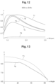
- FIG 12 is represented a graph analogous to the figure 7 , showing the evolution of the transmission (T1, T2, T3, T4, T5), for five devices (1, 2, 3, 4, 5) configured as in the Figures 1 to 5 , with a coating layer (20) of silicon dioxide SiO2 deposited on a substrate (10) of zinc selenide ZnSe.
- the wavelength (WL) varies from 0.8 to 3 ⁇ m, in the near and mid IR range.
- the transmission (T) varies from 0.7 to 1.
- the cavities (31) have a periodicity (L31) of 320 nm and a diameter (D31) of 265 nm.
- the cavities (31) have a depth (P31) of the order of 400 nm.
- the device (1) is well suited for the transmission of electromagnetic radiation in a near and mid IR wavelength range, between 0.8 and 3 ⁇ m.
- the transmission (T1) of the device (1) is improved compared to each of the devices (2, 3, 4, 5), at the level of the spectral width and the maximum transmission (therefore minimum absorption).
- the graph includes two curves showing the evolution of the transmission (T1, T2) as a function of the angle of incidence (Angle), for the devices (1, 2) described above in line with the figure 12 . It is observed that the angular transmission width is greater for device (1) than for device (2).
- FIG 14 is represented a graph analogous to the figure 7 , showing the evolution of the transmission (T1, T2, T3, T4, T5), for five devices (1, 2, 3, 4, 5) configured as in the Figures 1 to 5 , with a coating layer (20) of magnesium fluoride MgF2 deposited on a substrate (10) of silicon dioxide SiO2.
- the wavelength (WL) varies from 0.3 to 1 ⁇ m, in the visible, near and mid IR range.
- the transmission (T) varies from 0.96 to 1.
- the cavities (31) have a periodicity (L31) of 202 nm and a diameter (D31) of 160 nm.
- the cavities (31) have a depth (P31) of the order of 94 nm.
- the device (1) is well suited for the transmission of electromagnetic radiation in a visible wavelength range, between 0.38 and 0.78 ⁇ m.
- the transmission (T1) of the device (1) is improved compared to the transmissions (T2, T5) of the devices (2, 5), at the level of the spectral width and the maximum transmission (therefore minimum absorption).
- the transmission (T1) of the device (1) is relatively close to the transmissions (T3, T4) of the devices (3, 4).
- the graph includes two curves showing the evolution of the transmission (T1, T2) as a function of the angle of incidence (Angle), for the devices (1, 2) described above in line with the figure 14 . It is observed that the angular transmission width is greater for device (1) than for device (2).
- FIG 16 is represented a graph analogous to the figure 7 , showing the evolution of the transmission (T1, T2, T3, T4, T5), for five devices (1, 2, 3, 4, 5) configured as in the Figures 1 to 5 , with a coating layer (20) of silicon dioxide SiO2 deposited on a substrate (10) of alumina Al2O3.
- the wavelength (WL) varies from 0.3 to 1 ⁇ m, in the visible, near and mid IR range.
- the transmission (T) varies from 0.96 to 1.
- the cavities (31) have a periodicity (L31) of 176 nm and a diameter (D31) of 159 nm.
- the cavities (31) have a depth (P31) of the order of 156 nm.
- the device (1) is well suited for the transmission of electromagnetic radiation in a visible, near and mid IR wavelength range, between 0.3 and 1 ⁇ m.
- the transmission (T1) of the device (1) is improved compared to each of the devices (2, 3, 4, 5), at the level of the spectral width and the maximum transmission (therefore minimum absorption), in particular for a near and mid IR wavelength range.
- the cavities (31) are distributed on the surface of the device (1) with a variable periodicity. This variable periodicity evolves according to a defined rule and not randomly.
- the cavities (31) are distinct and not in communication with each other. The variations are controlled, they are not due to an irregular surface state of the device (1) and/or to the imprecisions of the texturing process.
- the periodicity is different between the center and the edges of the device (1).
- the cavities (31) are closer together in the center than on the edges.
- the cavities (31) have a symmetrical concave profile in an axial plane, with a diameter (D31) and a section of area decreasing with depth (P31).
- the cavities (31) have an asymmetrical concave profile in an axial plane, with a larger dimension (D31) and a decreasing area section with depth (P31). If the section is circular, the larger dimension (D31) is a diameter, otherwise for a non-circular section, the larger dimension (D31) is a length.
- the texturing (30) produces different optical effects depending on the orientation of the incident radiation. This phenomenon is reinforced by the asymmetry of the cavities (31).
- the cavities (31) have different depths (P31a, P31b).
- the cavities (31) have different diameters (D31a, D31b).
- the device (1) comprises a stack of two substrates (10) and two coating layers (20) in alternation.
- the cavities (31) are formed only in the first combination (10+20) of a substrate (10) and a coating layer (20), oriented on the upper side, receiving the incident radiation.
- this solution makes it possible to improve the wavefront correction, in comparison with a non-textured multilayer device.
- this solution represents a time saving compared with a multilayer device of which all the layers (20, 30) are crossed by the cavities (31), as described below.
- the device (1) also comprises a stack of two substrates (10) and two coating layers (20) alternately.
- the cavities (31) pass entirely through the stack except for the last substrate (10), which is partially hollowed out.
- the device (1) comprises a rear layer (40) made of a material different from the substrate (10) and the coating layer (20).
- the coating (20) is formed on a first side of the substrate (10), while the rear layer (40) is formed on a second side of the substrate (10) opposite the first side.
- the rear layer (40) has a different function from the coating layer (20).
- this rear layer (40) can provide anti-reflective and mechanical functions on the rear face, while the coating layer (20) has a broadband anti-reflective function.
- this rear layer (40) can be designed to reflect part of the radiation.
- the device (1) comprises two faces configured according to the invention, with a central substrate (10).
- Each face comprises a coating layer (20) and a texturing (30), forming cavities (31) which pass through the coating layer (20) and partially penetrate the substrate (10).
- the two coating layers (20) may be identical or different (materials, thicknesses, etc.).
- the behavior of a surface of the device (1) does not depend on the direction of the optical path. That is, the direction of passage of light from the air to the device (1) or from the device (1) to the air does not change the reflection and transmission rates of the device (1).
- the figure 28 schematically shows that under these conditions, whatever the direction of the device (1), then for incident optical radiation (I), the reflected (R) and transmitted (T) optical radiation are the same.
- the device (1) illustrated in the figure 25 can be considered as the assembly of two independent simple devices (1a, 1b) that have been juxtaposed.
- the transmission rate of the device (1) illustrated is then the multiplication of the transmission rates of these two independent simple devices.
- This configuration increases the performance of the device (1), since the optical system is thus equipped with a double wavefront correction device.
- This solution is advantageous for improving the wavefront correction, because it allows the use of both sides of the same device (1) to correctly correct the wavefront twice, instead of adding a second device in addition to the first.
- the overall size remains moderate.
- the device (1) comprises a first face configured according to the invention, with a coating layer (20) and a texturing (30) partially penetrating into the substrate (10), and a second face with a coating layer (20) which is devoid of texturing, or devoid of treatment, or receives a treatment different from the texturing of the first face.
- this configuration provides the equivalent of two complementary devices (1).
- the second side being adapted in terms of treatment or texturing, this solution allows you to choose the effect(s) you want to have, for one or more wavelength ranges.
- different treatments can be applied in the same wavelength range, for example a V-shaped antireflection treatment and a broadband antireflection treatment.
- different treatments can be applied in different wavelength ranges.
- the same treatment can be applied in two separate, juxtaposed or overlapping wavelength ranges. If the two wavelength ranges treated by each of the faces are juxtaposed or overlapping, the device (1) can be used to treat a larger range than with a single-sided device. Alternatively, if the two wavelength ranges treated by each of the faces are separate, the device (1) can act as a filter.
- the device (1) comprises two faces configured according to the invention, with a central layer (20/40).
- Each face comprises a coating layer (20) and a texturing (30), forming cavities (31) which pass through the coating layer (20) and partially penetrate the substrate (10).
- the substrate (10) and coating layers (20) of the two faces may be identical or different (materials, thicknesses, etc.).
- the device (1) comprises two stacks of substrate (10) and coating (20), as well as a back layer (40).
- the cavities (31) are formed only in the first combination (10+20) of a substrate (10) and a coating layer (20), oriented on the upper side, receiving the incident radiation. From such a configuration, several tests have been carried out.
- the device (1) according to the above configuration makes it possible to obtain improved transmission compared to the other two configurations, and over a much larger wavelength range.
- the device (1) according to the above configuration makes it possible to obtain an improved transmission compared to the two other configurations, and over a much larger wavelength range.
- the device (1) according to the above configuration makes it possible to obtain an improved transmission compared to the two other configurations, and over a much larger wavelength range.
- the device (1) according to the above configuration makes it possible to obtain an improved transmission compared to the two other configurations, and over a much larger wavelength range.
- the device (1) may be shaped differently from the Figures 1 to 37 without departing from the scope of the invention, which is defined by the claims. Furthermore, the technical characteristics of the various embodiments and variants mentioned above can be, in whole or in some cases, combined with each other. Thus, the device (1) can be adapted in terms of cost, functionality and performance.
Landscapes
- Physics & Mathematics (AREA)
- General Physics & Mathematics (AREA)
- Optics & Photonics (AREA)
- Health & Medical Sciences (AREA)
- Toxicology (AREA)
- Surface Treatment Of Optical Elements (AREA)
- Optical Elements Other Than Lenses (AREA)
- Optical Filters (AREA)
- Laminated Bodies (AREA)
- Glass Compositions (AREA)
- Optical Communication System (AREA)
Claims (15)
- Optisches Gerät (1), geeignet für die Übertragung/Reflexion von elektromagnetischer Strahlung in einem Wellenlängenbereich des elektromagnetischen Spektrums, der Infrarotstrahlung entspricht, ohne Beugungsordnung, wobei die Richtung des Lichtdurchgangs von der Luft zum Gerät (1) oder vom Gerät (1) zur Luft die Reflexions- und Transmissionsraten des Geräts (1) nicht verändert, wobei das Gerät (1) mindestens umfasst:- ein Substrat (10) aus einem ersten Material, das aus den folgenden Materialien ausgewählt ist: Silizium Si, Germanium Ge, Zinksulfid ZnS, Zinkselenid ZnSe,- eine Beschichtungsschicht (20), die auf einer ersten Seite des Substrats (10) gebildet ist und aus einem zweiten Material besteht, das sich von dem ersten Material unterscheidet, wobei dieses zweite Material aus den folgenden Materialien ausgewählt ist: Silizium Si, Germanium Ge, Zinksulfid ZnS, Zinkselenid ZnSe, Tantalpentoxid Ta2O5, Hafniumdioxid HfO2, Aluminiumoxid Al2O3, und- eine Oberflächenstrukturierung (30), die Hohlräume (31) im Gerät (1) bildet und den effektiven Brechungsindex auf der Oberfläche des Geräts variiert, wobei die Hohlräume (31) die Beschichtungsschicht (20) durchdringen und teilweise das Substrat (10) eingraben,- mindestens eine Rückseite-Schicht (40), die auf einer zweiten Seite des Substrats (10) gegenüber der ersten Seite gebildet ist und eine andere Funktion als die Beschichtungsschicht (20) hat, wobei das Material der Rückseite-Schicht sich vom Substrat (10) und der Beschichtung (20) unterscheidet und aus den folgenden Materialien ausgewählt ist: Silizium Si, Germanium Ge, Zinksulfid ZnS oder Zinkselenid ZnSe.
- Gerät (1) nach Anspruch 1, dadurch gekennzeichnet, dass die Hohlräume (31) ein durchgängiges Profil zwischen der Beschichtungsschicht (20) und dem Substrat (10) aufweisen.
- Gerät (1) nach Anspruch 1 oder 2, dadurch gekennzeichnet, dass die Hohlräume (31) einen kreisförmigen Querschnitt aufweisen.
- Gerät (1) nach einem der Ansprüche 1 bis 3, dadurch gekennzeichnet, dass die Hohlräume (31) ein konkaves Profil in einer axialen Ebene aufweisen, wobei die Querschnittsfläche mit der Tiefe abnimmt.
- Gerät (1) nach einem der Ansprüche 1 bis 4, dadurch gekennzeichnet, dass die Hohlräume (31) ein symmetrisches konkaves Profil in einer axialen Ebene aufweisen.
- Gerät (1) nach einem der Ansprüche 1 bis 4, dadurch gekennzeichnet, dass die Hohlräume (31) ein asymmetrisches konkaves Profil in einer axialen Ebene aufweisen.
- Gerät (1) nach einem der Ansprüche 1 bis 6, dadurch gekennzeichnet, dass die Hohlräume (31) in einem regelmäßigen Raster auf der Oberfläche des Geräts (1) angeordnet sind.
- Gerät (1) nach einem der vorhergehenden Ansprüche, dadurch gekennzeichnet, dass die Hohlräume (31) auf der Oberfläche des Geräts (1) mit variabler Periodizität angeordnet sind, die sich nach einer definierten Regel entwickelt und nicht zufällig ist, beispielsweise eine unterschiedliche Periodizität zwischen der Mitte und den Rändern des Geräts (1).
- Gerät (1) nach einem der vorhergehenden Ansprüche, dadurch gekennzeichnet, dass es einen Stapel aus mehreren Substraten (10) und Beschichtungsschichten (20) abwechselnd umfasst, wobei mindestens eine erste Kombination (10+20) aus einer ersten Beschichtungsschicht (20) und einem ersten Substrat (10) und eine letzte Kombination (10+20) aus einer letzten Beschichtungsschicht (20) und einem letzten Substrat (10) vorliegt.
- Gerät (1) nach Anspruch 9, dadurch gekennzeichnet, dass die Hohlräume (31) nur in der ersten Kombination (10+20) gebildet sind.
- Gerät (1) nach Anspruch 9, dadurch gekennzeichnet, dass die Hohlräume (31) den Stapel vollständig durchdringen, mit Ausnahme des letzten Substrats (10), das teilweise eingraviert ist, und dass die Hohlräume (31) eine streng abnehmende Querschnittsfläche in Richtung des letzten Substrats (10) aufweisen.
- Gerät (1) nach einem der Ansprüche 9 bis 11, dadurch gekennzeichnet, dass der Stapel mindestens eine Zwischenkombination (10+20) zwischen der ersten Kombination (10+20) und der letzten Kombination (10+20) umfasst.
- Gerät (1) nach einem der Ansprüche 1 bis 12, dadurch gekennzeichnet, dass es zwei Seiten umfasst, jede mit einer Beschichtungsschicht (20) und einer Oberflächenstrukturierung (30), die Hohlräume (31) bildet, die durch die Beschichtungsschicht hindurchgehen und teilweise das Substrat oder eines der Substrate durchdringen.
- Gerät (1) nach einem der Ansprüche 1 bis 12, dadurch gekennzeichnet, dass es eine erste Seite mit einer Beschichtungsschicht (20) und einer Oberflächenstrukturierung (30) aufweist, die Hohlräume (31) bildet, die durch die Beschichtungsschicht (20) hindurchgehen und teilweise das Substrat (10) oder eines der Substrate (10) durchdringen, und eine zweite Seite mit einer Beschichtungsschicht (20), die keine Strukturierung aufweist, nicht behandelt ist oder eine andere Behandlung erhält als die Strukturierung der ersten Seite.
- Verfahren zur Herstellung eines optischen Geräts, geeignet für die Übertragung/Reflexion von elektromagnetischer Strahlung in einem Wellenlängenbereich des elektromagnetischen Spektrums, der Infrarotstrahlung entspricht, wobei die Richtung des Lichtdurchgangs von der Luft zum Gerät (1) oder vom Gerät (1) zur Luft die Reflexions- und Transmissionsraten des Geräts (1) nicht verändert, wobei das Verfahren mindestens die folgenden Schritte umfasst:- Bilden von mindestens einer Kombination:* eines Substrats, das aus einem ersten Material ausgewählt ist, das zu den folgenden gehört: Silizium Si, Germanium Ge, Zinksulfid ZnS, Zinkselenid ZnSe,* einer Beschichtungsschicht, die aus einem zweiten Material besteht, das sich von dem ersten Material unterscheidet, wobei dieses zweite Material aus den folgenden Materialien ausgewählt ist: Silizium Si, Germanium Ge, Zinksulfid ZnS, Zinkselenid ZnSe, Tantalpentoxid Ta2O5, Hafniumdioxid HfO2, Aluminiumoxid Al2O3, und* einer Rückseite-Schicht, die eine andere Funktion als die der Beschichtungsschicht (20) hat, aus einem Material besteht, das sich von dem Substrat und der Beschichtung unterscheidet, und aus den folgenden Materialien ausgewählt ist: Silizium Si, Germanium Ge, Zinksulfid ZnS oder Zinkselenid ZnSe, wobei die Beschichtung auf einer ersten Seite des Substrats gebildet wird, die Rückseite-Schicht auf einer zweiten Seite des Substrats gegenüber der ersten Seite gebildet wird, und anschließend- eine Oberflächenstrukturierung durchführen, die Hohlräume im Gerät bildet und den effektiven Brechungsindex auf der Oberfläche des Geräts variiert, wobei die Hohlräume die Beschichtungsschicht durchdringen und teilweise das Substrat eingraben.
Applications Claiming Priority (5)
| Application Number | Priority Date | Filing Date | Title |
|---|---|---|---|
| FR1911937A FR3102565B1 (fr) | 2019-10-24 | 2019-10-24 | Dispositif optique avec une texturation de surface |
| FR2010389A FR3102567B1 (fr) | 2019-10-24 | 2020-10-12 | Dispositif optique |
| FR2010388A FR3102566B1 (fr) | 2019-10-24 | 2020-10-12 | Dispositif optique |
| FR2010382A FR3102574B1 (fr) | 2019-10-24 | 2020-10-12 | Dispositif optique adapté à la transmission/réflexion d'un rayonnement électromagnétique |
| PCT/FR2020/051933 WO2021079077A1 (fr) | 2019-10-24 | 2020-10-26 | Dispositif optique |
Publications (2)
| Publication Number | Publication Date |
|---|---|
| EP4022364A1 EP4022364A1 (de) | 2022-07-06 |
| EP4022364B1 true EP4022364B1 (de) | 2024-12-04 |
Family
ID=75617151
Family Applications (2)
| Application Number | Title | Priority Date | Filing Date |
|---|---|---|---|
| EP20808492.1A Active EP4022364B1 (de) | 2019-10-24 | 2020-10-26 | Optische vorrichtung |
| EP20808181.0A Active EP4022363B1 (de) | 2019-10-24 | 2020-10-26 | Optische vorrichtung |
Family Applications After (1)
| Application Number | Title | Priority Date | Filing Date |
|---|---|---|---|
| EP20808181.0A Active EP4022363B1 (de) | 2019-10-24 | 2020-10-26 | Optische vorrichtung |
Country Status (12)
| Country | Link |
|---|---|
| US (2) | US12392934B2 (de) |
| EP (2) | EP4022364B1 (de) |
| JP (3) | JP2023507873A (de) |
| KR (2) | KR102798391B1 (de) |
| CN (3) | CN120405812A (de) |
| DK (2) | DK4022364T3 (de) |
| ES (2) | ES2999209T3 (de) |
| FI (2) | FI4022364T3 (de) |
| FR (4) | FR3102565B1 (de) |
| IL (2) | IL292368B1 (de) |
| LT (2) | LT4022363T (de) |
| WO (2) | WO2021079077A1 (de) |
Families Citing this family (1)
| Publication number | Priority date | Publication date | Assignee | Title |
|---|---|---|---|---|
| US20230051264A1 (en) * | 2021-08-12 | 2023-02-16 | Teledyne Flir Commercial Systems, Inc. | Superhydrophobic surface in thermal infrared imaging device |
Citations (1)
| Publication number | Priority date | Publication date | Assignee | Title |
|---|---|---|---|---|
| US20080074748A1 (en) * | 2006-09-21 | 2008-03-27 | Nippon Sheet Glass Company, Limited | Transmissive diffraction grating, and spectral separation element and spectroscope using the same |
Family Cites Families (29)
| Publication number | Priority date | Publication date | Assignee | Title |
|---|---|---|---|---|
| JPS564896A (en) * | 1979-06-22 | 1981-01-19 | Tamura Electric Works Ltd | Emergency annunciator |
| JP2004077806A (ja) * | 2002-08-19 | 2004-03-11 | Sanyo Electric Co Ltd | 位相板光学素子 |
| JP2004109432A (ja) * | 2002-09-18 | 2004-04-08 | Mitsubishi Electric Corp | シリコン構造体およびその製造方法 |
| US20060256428A1 (en) * | 2005-05-16 | 2006-11-16 | Lake Shore Cryotronics, Inc. | Long wave pass infrared filter based on porous semiconductor material and the method of manufacturing the same |
| US8535616B2 (en) * | 2005-08-02 | 2013-09-17 | Moxtek, Inc. | Sub-wavelength metallic apertures as light enhancement devices |
| JP2007069604A (ja) * | 2005-08-10 | 2007-03-22 | Toray Ind Inc | パターン形成方法、パターン形成用シート、およびそれを用いて形成される光学機能性シート |
| EP1785748A1 (de) * | 2005-11-10 | 2007-05-16 | C.R.F. Società Consortile per Azioni | Nanometrische antireflektive Struktur basierend auf poröses anodisches Aluminiumoxid, und Vefahren zu deren Herstellung |
| JP5016872B2 (ja) * | 2006-08-30 | 2012-09-05 | キヤノン電子株式会社 | 光学フィルタ |
| JP5280654B2 (ja) * | 2006-09-21 | 2013-09-04 | 日本板硝子株式会社 | 透過型回折格子、並びに、それを用いた分光素子及び分光器 |
| JP4842763B2 (ja) * | 2006-10-23 | 2011-12-21 | 株式会社リコー | 光学素子および光学装置 |
| JP2008164996A (ja) | 2006-12-28 | 2008-07-17 | Nissan Motor Co Ltd | 発色性反射防止構造及び構造体 |
| WO2009051595A1 (en) * | 2007-10-18 | 2009-04-23 | Midwest Research Institue | High temperature solar selective coatings |
| KR101081499B1 (ko) * | 2009-08-19 | 2011-11-08 | 광주과학기술원 | 무반사 나노구조의 제조방법 |
| CN101726769B (zh) * | 2009-12-16 | 2011-11-16 | 中国科学院苏州纳米技术与纳米仿生研究所 | 叠层亚波长减反结构及其制备方法 |
| JP5659551B2 (ja) * | 2010-04-28 | 2015-01-28 | ソニー株式会社 | 透明導電性素子、入力装置、および表示装置 |
| JP5658484B2 (ja) * | 2010-05-28 | 2015-01-28 | リコー光学株式会社 | 反射型波長板 |
| FR2975506B1 (fr) | 2011-05-19 | 2013-08-09 | Thales Sa | Composant optique avec empilement de structures micro ou nanostructurees |
| DE202011110173U1 (de) * | 2011-07-13 | 2013-03-15 | Fraunhofer-Gesellschaft zur Förderung der angewandten Forschung e.V. | Optisches Element mit einer Antireflexionsbeschichtung |
| DE102011112696B4 (de) * | 2011-08-31 | 2016-02-18 | Martin-Luther-Universität Halle-Wittenberg | Solarzelle mit Folie zur Rückseitenkontaktierung, Verfahren zu deren Herstellung und Verwendung einer Folie als Rückseitenkontaktierung |
| CN104160311A (zh) | 2012-01-04 | 2014-11-19 | 瑞达克斯科技有限公司 | 使用纳米多孔结晶材料的光学薄膜层之结构及方法 |
| EP2828629B1 (de) * | 2012-03-23 | 2021-06-16 | Fraunhofer Gesellschaft zur Förderung der angewandten Forschung e.V. | Mikrovorrichtung mit elektromagnetischer strahlung, wafer-element und verfahren zur herstellung eines derartigen mikrovorrichtung |
| EP2983015B1 (de) * | 2013-04-02 | 2021-10-27 | Panasonic Intellectual Property Management Co., Ltd. | Optisches element |
| US20150103396A1 (en) * | 2013-05-01 | 2015-04-16 | Byron Zollars | Antireflective Structures for Optics |
| JP6903418B2 (ja) * | 2015-11-16 | 2021-07-14 | デクセリアルズ株式会社 | 光学体、原盤、及び光学体の製造方法 |
| FR3047810B1 (fr) | 2016-02-12 | 2018-05-25 | Thales | Composant diffractif sub longueur d'onde large bande spectracle |
| JP2018194620A (ja) * | 2017-05-15 | 2018-12-06 | Jsr株式会社 | 光学フィルター |
| JPWO2019004199A1 (ja) * | 2017-06-28 | 2020-04-30 | マクセルホールディングス株式会社 | 透明遮熱断熱部材及びその製造方法 |
| JP6401837B1 (ja) * | 2017-08-10 | 2018-10-10 | デクセリアルズ株式会社 | 偏光板及び光学機器 |
| US10712475B2 (en) * | 2017-08-16 | 2020-07-14 | Lumentum Operations Llc | Multi-layer thin film stack for diffractive optical elements |
-
2019
- 2019-10-24 FR FR1911937A patent/FR3102565B1/fr active Active
-
2020
- 2020-10-12 FR FR2010389A patent/FR3102567B1/fr active Active
- 2020-10-12 FR FR2010382A patent/FR3102574B1/fr active Active
- 2020-10-12 FR FR2010388A patent/FR3102566B1/fr active Active
- 2020-10-26 IL IL292368A patent/IL292368B1/en unknown
- 2020-10-26 FI FIEP20808492.1T patent/FI4022364T3/en active
- 2020-10-26 DK DK20808492.1T patent/DK4022364T3/da active
- 2020-10-26 FI FIEP20808181.0T patent/FI4022363T3/en active
- 2020-10-26 ES ES20808492T patent/ES2999209T3/es active Active
- 2020-10-26 CN CN202510722668.5A patent/CN120405812A/zh active Pending
- 2020-10-26 KR KR1020227017148A patent/KR102798391B1/ko active Active
- 2020-10-26 EP EP20808492.1A patent/EP4022364B1/de active Active
- 2020-10-26 CN CN202080074440.5A patent/CN114600005A/zh active Pending
- 2020-10-26 WO PCT/FR2020/051933 patent/WO2021079077A1/fr not_active Ceased
- 2020-10-26 IL IL292369A patent/IL292369B1/en unknown
- 2020-10-26 EP EP20808181.0A patent/EP4022363B1/de active Active
- 2020-10-26 KR KR1020227017149A patent/KR102781754B1/ko active Active
- 2020-10-26 LT LTEPPCT/FR2020/051934T patent/LT4022363T/lt unknown
- 2020-10-26 ES ES20808181T patent/ES3034149T3/es active Active
- 2020-10-26 JP JP2022524164A patent/JP2023507873A/ja active Pending
- 2020-10-26 WO PCT/FR2020/051934 patent/WO2021079078A1/fr not_active Ceased
- 2020-10-26 JP JP2022524166A patent/JP7594005B2/ja active Active
- 2020-10-26 DK DK20808181.0T patent/DK4022363T3/da active
- 2020-10-26 US US17/771,505 patent/US12392934B2/en active Active
- 2020-10-26 US US17/771,504 patent/US12287453B2/en active Active
- 2020-10-26 CN CN202080074431.6A patent/CN114600004A/zh active Pending
- 2020-10-26 LT LTEPPCT/FR2020/051933T patent/LT4022364T/lt unknown
-
2024
- 2024-09-06 JP JP2024154005A patent/JP2024161268A/ja active Pending
Patent Citations (1)
| Publication number | Priority date | Publication date | Assignee | Title |
|---|---|---|---|---|
| US20080074748A1 (en) * | 2006-09-21 | 2008-03-27 | Nippon Sheet Glass Company, Limited | Transmissive diffraction grating, and spectral separation element and spectroscope using the same |
Also Published As
Similar Documents
| Publication | Publication Date | Title |
|---|---|---|
| EP2613181B1 (de) | Infrarotdetektor mit gehäuse mit mindestens einem integrierten beugungsgitter | |
| EP4022364B1 (de) | Optische vorrichtung | |
| WO2011157809A1 (fr) | Ecran phosphore a fibres optiques comportant un filtre angulaire | |
| WO2015040288A1 (fr) | Dispositif catadioptrique améliorant la visualisation d'une image placée devant un capteur solaire | |
| EP4416535A1 (de) | Optisches antireflexionselement | |
| RU2798743C1 (ru) | Оптическое устройство | |
| RU2800647C1 (ru) | Оптическое устройство | |
| WO2024052607A1 (fr) | Filtre spectral a resonateurs couples | |
| FR3147388A1 (fr) | Elément optique antireflet | |
| FR3152606A1 (fr) | Filtre multispectral pour une radiation électromagnétique et procédé de fabrication dudit filtre | |
| EP2092380A2 (de) | Schaltbares optisches filter mit photonischen kristallen |
Legal Events
| Date | Code | Title | Description |
|---|---|---|---|
| STAA | Information on the status of an ep patent application or granted ep patent |
Free format text: STATUS: UNKNOWN |
|
| STAA | Information on the status of an ep patent application or granted ep patent |
Free format text: STATUS: THE INTERNATIONAL PUBLICATION HAS BEEN MADE |
|
| PUAI | Public reference made under article 153(3) epc to a published international application that has entered the european phase |
Free format text: ORIGINAL CODE: 0009012 |
|
| STAA | Information on the status of an ep patent application or granted ep patent |
Free format text: STATUS: REQUEST FOR EXAMINATION WAS MADE |
|
| 17P | Request for examination filed |
Effective date: 20220401 |
|
| AK | Designated contracting states |
Kind code of ref document: A1 Designated state(s): AL AT BE BG CH CY CZ DE DK EE ES FI FR GB GR HR HU IE IS IT LI LT LU LV MC MK MT NL NO PL PT RO RS SE SI SK SM TR |
|
| STAA | Information on the status of an ep patent application or granted ep patent |
Free format text: STATUS: EXAMINATION IS IN PROGRESS |
|
| DAV | Request for validation of the european patent (deleted) | ||
| DAX | Request for extension of the european patent (deleted) | ||
| 17Q | First examination report despatched |
Effective date: 20230207 |
|
| P01 | Opt-out of the competence of the unified patent court (upc) registered |
Effective date: 20230527 |
|
| GRAP | Despatch of communication of intention to grant a patent |
Free format text: ORIGINAL CODE: EPIDOSNIGR1 |
|
| GRAP | Despatch of communication of intention to grant a patent |
Free format text: ORIGINAL CODE: EPIDOSNIGR1 |
|
| STAA | Information on the status of an ep patent application or granted ep patent |
Free format text: STATUS: GRANT OF PATENT IS INTENDED |
|
| INTG | Intention to grant announced |
Effective date: 20240614 |
|
| GRAS | Grant fee paid |
Free format text: ORIGINAL CODE: EPIDOSNIGR3 |
|
| GRAA | (expected) grant |
Free format text: ORIGINAL CODE: 0009210 |
|
| STAA | Information on the status of an ep patent application or granted ep patent |
Free format text: STATUS: THE PATENT HAS BEEN GRANTED |
|
| AK | Designated contracting states |
Kind code of ref document: B1 Designated state(s): AL AT BE BG CH CY CZ DE DK EE ES FI FR GB GR HR HU IE IS IT LI LT LU LV MC MK MT NL NO PL PT RO RS SE SI SK SM TR |
|
| REG | Reference to a national code |
Ref country code: DK Ref legal event code: T3 Effective date: 20241206 |
|
| REG | Reference to a national code |
Ref country code: NL Ref legal event code: FP |
|
| REG | Reference to a national code |
Ref country code: CH Ref legal event code: EP |
|
| REG | Reference to a national code |
Ref country code: DE Ref legal event code: R096 Ref document number: 602020042636 Country of ref document: DE |
|
| REG | Reference to a national code |
Ref country code: IE Ref legal event code: FG4D Free format text: LANGUAGE OF EP DOCUMENT: FRENCH |
|
| REG | Reference to a national code |
Ref country code: FI Ref legal event code: FGE |
|
| REG | Reference to a national code |
Ref country code: ES Ref legal event code: FG2A Ref document number: 2999209 Country of ref document: ES Kind code of ref document: T3 Effective date: 20250225 |
|
| PG25 | Lapsed in a contracting state [announced via postgrant information from national office to epo] |
Ref country code: HR Free format text: LAPSE BECAUSE OF FAILURE TO SUBMIT A TRANSLATION OF THE DESCRIPTION OR TO PAY THE FEE WITHIN THE PRESCRIBED TIME-LIMIT Effective date: 20241204 |
|
| PG25 | Lapsed in a contracting state [announced via postgrant information from national office to epo] |
Ref country code: BG Free format text: LAPSE BECAUSE OF FAILURE TO SUBMIT A TRANSLATION OF THE DESCRIPTION OR TO PAY THE FEE WITHIN THE PRESCRIBED TIME-LIMIT Effective date: 20241204 |
|
| PG25 | Lapsed in a contracting state [announced via postgrant information from national office to epo] |
Ref country code: NO Free format text: LAPSE BECAUSE OF FAILURE TO SUBMIT A TRANSLATION OF THE DESCRIPTION OR TO PAY THE FEE WITHIN THE PRESCRIBED TIME-LIMIT Effective date: 20250304 |
|
| PG25 | Lapsed in a contracting state [announced via postgrant information from national office to epo] |
Ref country code: LV Free format text: LAPSE BECAUSE OF FAILURE TO SUBMIT A TRANSLATION OF THE DESCRIPTION OR TO PAY THE FEE WITHIN THE PRESCRIBED TIME-LIMIT Effective date: 20241204 Ref country code: GR Free format text: LAPSE BECAUSE OF FAILURE TO SUBMIT A TRANSLATION OF THE DESCRIPTION OR TO PAY THE FEE WITHIN THE PRESCRIBED TIME-LIMIT Effective date: 20250305 |
|
| PG25 | Lapsed in a contracting state [announced via postgrant information from national office to epo] |
Ref country code: RS Free format text: LAPSE BECAUSE OF FAILURE TO SUBMIT A TRANSLATION OF THE DESCRIPTION OR TO PAY THE FEE WITHIN THE PRESCRIBED TIME-LIMIT Effective date: 20250304 |
|
| REG | Reference to a national code |
Ref country code: AT Ref legal event code: MK05 Ref document number: 1748738 Country of ref document: AT Kind code of ref document: T Effective date: 20241204 |
|
| PG25 | Lapsed in a contracting state [announced via postgrant information from national office to epo] |
Ref country code: SM Free format text: LAPSE BECAUSE OF FAILURE TO SUBMIT A TRANSLATION OF THE DESCRIPTION OR TO PAY THE FEE WITHIN THE PRESCRIBED TIME-LIMIT Effective date: 20241204 |
|
| PG25 | Lapsed in a contracting state [announced via postgrant information from national office to epo] |
Ref country code: PL Free format text: LAPSE BECAUSE OF FAILURE TO SUBMIT A TRANSLATION OF THE DESCRIPTION OR TO PAY THE FEE WITHIN THE PRESCRIBED TIME-LIMIT Effective date: 20241204 |
|
| PG25 | Lapsed in a contracting state [announced via postgrant information from national office to epo] |
Ref country code: IS Free format text: LAPSE BECAUSE OF FAILURE TO SUBMIT A TRANSLATION OF THE DESCRIPTION OR TO PAY THE FEE WITHIN THE PRESCRIBED TIME-LIMIT Effective date: 20250404 |
|
| PG25 | Lapsed in a contracting state [announced via postgrant information from national office to epo] |
Ref country code: PT Free format text: LAPSE BECAUSE OF FAILURE TO SUBMIT A TRANSLATION OF THE DESCRIPTION OR TO PAY THE FEE WITHIN THE PRESCRIBED TIME-LIMIT Effective date: 20250404 |
|
| PG25 | Lapsed in a contracting state [announced via postgrant information from national office to epo] |
Ref country code: EE Free format text: LAPSE BECAUSE OF FAILURE TO SUBMIT A TRANSLATION OF THE DESCRIPTION OR TO PAY THE FEE WITHIN THE PRESCRIBED TIME-LIMIT Effective date: 20241204 |
|
| PG25 | Lapsed in a contracting state [announced via postgrant information from national office to epo] |
Ref country code: AT Free format text: LAPSE BECAUSE OF FAILURE TO SUBMIT A TRANSLATION OF THE DESCRIPTION OR TO PAY THE FEE WITHIN THE PRESCRIBED TIME-LIMIT Effective date: 20241204 |
|
| PG25 | Lapsed in a contracting state [announced via postgrant information from national office to epo] |
Ref country code: SK Free format text: LAPSE BECAUSE OF FAILURE TO SUBMIT A TRANSLATION OF THE DESCRIPTION OR TO PAY THE FEE WITHIN THE PRESCRIBED TIME-LIMIT Effective date: 20241204 |
|
| PG25 | Lapsed in a contracting state [announced via postgrant information from national office to epo] |
Ref country code: CZ Free format text: LAPSE BECAUSE OF FAILURE TO SUBMIT A TRANSLATION OF THE DESCRIPTION OR TO PAY THE FEE WITHIN THE PRESCRIBED TIME-LIMIT Effective date: 20241204 |
|
| REG | Reference to a national code |
Ref country code: DE Ref legal event code: R097 Ref document number: 602020042636 Country of ref document: DE |
|
| PG25 | Lapsed in a contracting state [announced via postgrant information from national office to epo] |
Ref country code: SE Free format text: LAPSE BECAUSE OF FAILURE TO SUBMIT A TRANSLATION OF THE DESCRIPTION OR TO PAY THE FEE WITHIN THE PRESCRIBED TIME-LIMIT Effective date: 20241204 |
|
| PGFP | Annual fee paid to national office [announced via postgrant information from national office to epo] |
Ref country code: FI Payment date: 20250922 Year of fee payment: 6 |
|
| PGFP | Annual fee paid to national office [announced via postgrant information from national office to epo] |
Ref country code: LT Payment date: 20250923 Year of fee payment: 6 Ref country code: DK Payment date: 20250930 Year of fee payment: 6 |
|
| PLBE | No opposition filed within time limit |
Free format text: ORIGINAL CODE: 0009261 |
|
| STAA | Information on the status of an ep patent application or granted ep patent |
Free format text: STATUS: NO OPPOSITION FILED WITHIN TIME LIMIT |
|
| PGFP | Annual fee paid to national office [announced via postgrant information from national office to epo] |
Ref country code: NL Payment date: 20250926 Year of fee payment: 6 |
|
| REG | Reference to a national code |
Ref country code: CH Ref legal event code: L10 Free format text: ST27 STATUS EVENT CODE: U-0-0-L10-L00 (AS PROVIDED BY THE NATIONAL OFFICE) Effective date: 20251015 |
|
| REG | Reference to a national code |
Ref country code: CH Ref legal event code: U11 Free format text: ST27 STATUS EVENT CODE: U-0-0-U10-U11 (AS PROVIDED BY THE NATIONAL OFFICE) Effective date: 20251101 |
|
| 26N | No opposition filed |
Effective date: 20250905 |
|
| PGFP | Annual fee paid to national office [announced via postgrant information from national office to epo] |
Ref country code: DE Payment date: 20251015 Year of fee payment: 6 |
|
| PGFP | Annual fee paid to national office [announced via postgrant information from national office to epo] |
Ref country code: GB Payment date: 20251023 Year of fee payment: 6 |
|
| PGFP | Annual fee paid to national office [announced via postgrant information from national office to epo] |
Ref country code: IT Payment date: 20251007 Year of fee payment: 6 |
|
| PGFP | Annual fee paid to national office [announced via postgrant information from national office to epo] |
Ref country code: FR Payment date: 20251031 Year of fee payment: 6 |
|
| PGFP | Annual fee paid to national office [announced via postgrant information from national office to epo] |
Ref country code: TR Payment date: 20251017 Year of fee payment: 6 |
|
| PGFP | Annual fee paid to national office [announced via postgrant information from national office to epo] |
Ref country code: CH Payment date: 20251101 Year of fee payment: 6 |
|
| PGFP | Annual fee paid to national office [announced via postgrant information from national office to epo] |
Ref country code: RO Payment date: 20251001 Year of fee payment: 6 |
|
| PGFP | Annual fee paid to national office [announced via postgrant information from national office to epo] |
Ref country code: ES Payment date: 20251110 Year of fee payment: 6 |