EP4016641B1 - Halbleiterbauelement und layout für gate-elektroden - Google Patents
Halbleiterbauelement und layout für gate-elektroden Download PDFInfo
- Publication number
- EP4016641B1 EP4016641B1 EP21192097.0A EP21192097A EP4016641B1 EP 4016641 B1 EP4016641 B1 EP 4016641B1 EP 21192097 A EP21192097 A EP 21192097A EP 4016641 B1 EP4016641 B1 EP 4016641B1
- Authority
- EP
- European Patent Office
- Prior art keywords
- gate electrode
- region
- electrode
- gate
- silicon carbide
- Prior art date
- Legal status (The legal status is an assumption and is not a legal conclusion. Google has not performed a legal analysis and makes no representation as to the accuracy of the status listed.)
- Active
Links
Images







Classifications
-
- H—ELECTRICITY
- H10—SEMICONDUCTOR DEVICES; ELECTRIC SOLID-STATE DEVICES NOT OTHERWISE PROVIDED FOR
- H10D—INORGANIC ELECTRIC SEMICONDUCTOR DEVICES
- H10D30/00—Field-effect transistors [FET]
- H10D30/60—Insulated-gate field-effect transistors [IGFET]
- H10D30/611—Insulated-gate field-effect transistors [IGFET] having multiple independently-addressable gate electrodes influencing the same channel
-
- H—ELECTRICITY
- H10—SEMICONDUCTOR DEVICES; ELECTRIC SOLID-STATE DEVICES NOT OTHERWISE PROVIDED FOR
- H10D—INORGANIC ELECTRIC SEMICONDUCTOR DEVICES
- H10D64/00—Electrodes of devices having potential barriers
- H10D64/20—Electrodes characterised by their shapes, relative sizes or dispositions
- H10D64/27—Electrodes not carrying the current to be rectified, amplified, oscillated or switched, e.g. gates
- H10D64/311—Gate electrodes for field-effect devices
- H10D64/411—Gate electrodes for field-effect devices for FETs
- H10D64/511—Gate electrodes for field-effect devices for FETs for IGFETs
- H10D64/517—Gate electrodes for field-effect devices for FETs for IGFETs characterised by the conducting layers
- H10D64/519—Gate electrodes for field-effect devices for FETs for IGFETs characterised by the conducting layers characterised by their top-view geometrical layouts
-
- H—ELECTRICITY
- H10—SEMICONDUCTOR DEVICES; ELECTRIC SOLID-STATE DEVICES NOT OTHERWISE PROVIDED FOR
- H10D—INORGANIC ELECTRIC SEMICONDUCTOR DEVICES
- H10D30/00—Field-effect transistors [FET]
- H10D30/60—Insulated-gate field-effect transistors [IGFET]
- H10D30/63—Vertical IGFETs
-
- H—ELECTRICITY
- H10—SEMICONDUCTOR DEVICES; ELECTRIC SOLID-STATE DEVICES NOT OTHERWISE PROVIDED FOR
- H10D—INORGANIC ELECTRIC SEMICONDUCTOR DEVICES
- H10D30/00—Field-effect transistors [FET]
- H10D30/60—Insulated-gate field-effect transistors [IGFET]
- H10D30/64—Double-diffused metal-oxide semiconductor [DMOS] FETs
- H10D30/66—Vertical DMOS [VDMOS] FETs
-
- H—ELECTRICITY
- H10—SEMICONDUCTOR DEVICES; ELECTRIC SOLID-STATE DEVICES NOT OTHERWISE PROVIDED FOR
- H10D—INORGANIC ELECTRIC SEMICONDUCTOR DEVICES
- H10D62/00—Semiconductor bodies, or regions thereof, of devices having potential barriers
- H10D62/80—Semiconductor bodies, or regions thereof, of devices having potential barriers characterised by the materials
- H10D62/83—Semiconductor bodies, or regions thereof, of devices having potential barriers characterised by the materials being Group IV materials, e.g. B-doped Si or undoped Ge
- H10D62/832—Semiconductor bodies, or regions thereof, of devices having potential barriers characterised by the materials being Group IV materials, e.g. B-doped Si or undoped Ge being Group IV materials comprising two or more elements, e.g. SiGe
- H10D62/8325—Silicon carbide
-
- H—ELECTRICITY
- H10—SEMICONDUCTOR DEVICES; ELECTRIC SOLID-STATE DEVICES NOT OTHERWISE PROVIDED FOR
- H10D—INORGANIC ELECTRIC SEMICONDUCTOR DEVICES
- H10D84/00—Integrated devices formed in or on semiconductor substrates that comprise only semiconducting layers, e.g. on Si wafers or on GaAs-on-Si wafers
- H10D84/101—Integrated devices comprising main components and built-in components, e.g. IGBT having built-in freewheel diode
- H10D84/141—VDMOS having built-in components
- H10D84/146—VDMOS having built-in components the built-in components being Schottky barrier diodes
-
- H—ELECTRICITY
- H10—SEMICONDUCTOR DEVICES; ELECTRIC SOLID-STATE DEVICES NOT OTHERWISE PROVIDED FOR
- H10D—INORGANIC ELECTRIC SEMICONDUCTOR DEVICES
- H10D84/00—Integrated devices formed in or on semiconductor substrates that comprise only semiconducting layers, e.g. on Si wafers or on GaAs-on-Si wafers
- H10D84/80—Integrated devices formed in or on semiconductor substrates that comprise only semiconducting layers, e.g. on Si wafers or on GaAs-on-Si wafers characterised by the integration of at least one component covered by groups H10D12/00 or H10D30/00, e.g. integration of IGFETs
- H10D84/82—Integrated devices formed in or on semiconductor substrates that comprise only semiconducting layers, e.g. on Si wafers or on GaAs-on-Si wafers characterised by the integration of at least one component covered by groups H10D12/00 or H10D30/00, e.g. integration of IGFETs of only field-effect components
- H10D84/83—Integrated devices formed in or on semiconductor substrates that comprise only semiconducting layers, e.g. on Si wafers or on GaAs-on-Si wafers characterised by the integration of at least one component covered by groups H10D12/00 or H10D30/00, e.g. integration of IGFETs of only field-effect components of only insulated-gate FETs [IGFET]
-
- H—ELECTRICITY
- H10—SEMICONDUCTOR DEVICES; ELECTRIC SOLID-STATE DEVICES NOT OTHERWISE PROVIDED FOR
- H10D—INORGANIC ELECTRIC SEMICONDUCTOR DEVICES
- H10D84/00—Integrated devices formed in or on semiconductor substrates that comprise only semiconducting layers, e.g. on Si wafers or on GaAs-on-Si wafers
- H10D84/101—Integrated devices comprising main components and built-in components, e.g. IGBT having built-in freewheel diode
- H10D84/141—VDMOS having built-in components
- H10D84/143—VDMOS having built-in components the built-in components being PN junction diodes
- H10D84/144—VDMOS having built-in components the built-in components being PN junction diodes in antiparallel diode configurations
-
- H—ELECTRICITY
- H10—SEMICONDUCTOR DEVICES; ELECTRIC SOLID-STATE DEVICES NOT OTHERWISE PROVIDED FOR
- H10W—GENERIC PACKAGES, INTERCONNECTIONS, CONNECTORS OR OTHER CONSTRUCTIONAL DETAILS OF DEVICES COVERED BY CLASS H10
- H10W72/00—Interconnections or connectors in packages
- H10W72/90—Bond pads, in general
- H10W72/921—Structures or relative sizes of bond pads
- H10W72/926—Multiple bond pads having different sizes
Definitions
- a plurality of gate electrodes arranged in a stripe pattern are provided in the MOSFET.
- the plurality of gate electrodes are connected to, for example, one gate wiring line, and a gate voltage is applied to the gate wiring line to drive the MOSFET.
- the present invention provides a semiconductor device, in accordance with claim 1. Preferred embodiments are set out in the dependent claims.
- n + , n, n - , p + , p, and p - these are assumed to indicate the relative high and low of the impurity concentration in each conductive type. That is, n + indicates that the n-type impurity concentration is relatively higher than n, and n - indicates that the n-type impurity concentration is relatively lower than n. In addition, p + indicates that the p-type impurity concentration is relatively higher than p, and p - indicates that the p-type impurity concentration is relatively lower than p. In addition, n + -type and n - -type may be simply described as n-type, p + -type and p - -type may be simply described as p-type.
- the impurity concentration can be measured by, for example, secondary ion mass spectrometry (SIMS).
- SIMS secondary ion mass spectrometry
- the relative difference of the impurity concentration can be determined from, for example, the difference of the carrier concentration obtained by scanning capacitance microscopy (SCM).
- SCM scanning capacitance microscopy
- the distance such as the depth and thickness of an impurity region can be calculated by, for example, SIMS.
- the distance such as the depth, thickness, and width of an impurity region and a distance between impurity regions can be calculated, for example, by using an SCM image and SIMS measurement results.
- the width of a conductive layer, a distance between conductive layers, the thickness of an insulating layer, and the like can be measured on, for example, an image of a scanning electron microscope (SEM) or a transmission electron microscope (TEM).
- a semiconductor device of a first embodiment includes: a first electrode; a second electrode; a silicon carbide layer provided between the first electrode and the second electrode and including a first silicon carbide region of a first conductive type, a second silicon carbide region of a second conductive type provided between the first electrode and the first silicon carbide region, and a third silicon carbide region of a first conductive type provided between the first electrode and the second silicon carbide region; a first gate electrode provided between the first electrode and the silicon carbide layer and extending in a first direction; a second gate electrode provided between the first electrode and the silicon carbide layer and extending in the first direction; a third gate electrode provided between the first electrode and the silicon carbide layer and extending in the first direction; a gate wiring line provided between the first electrode and the silicon carbide layer and extending in a second direction crossing the first direction, the first gate electrode, the second gate electrode, and the third gate electrode being connected to the gate wiring line; and a gate insulating layer provided between the first gate electrode and the silicon carbide layer, between
- Fig. 1 is a schematic top view of the semiconductor device of the first embodiment.
- Fig. 2 is an enlarged schematic top view of the semiconductor device of the first embodiment.
- Fig. 2 is an enlarged view of a region X surrounded by the dotted line in Fig. 1 .
- Fig. 2 shows a pattern layout of a gate electrode and a gate wiring line.
- the semiconductor device of the first embodiment is a planar gate type vertical MOSFET 100 using silicon carbide.
- the MOSFET 100 is, for example, a double implantation MOSFET (DIMOSFET) in which a body region and a source region are formed by ion implantation.
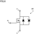
- the MOSFET 100 includes a Schottky barrier diode (SBD) as a built-in diode.
- SBD Schottky barrier diode
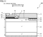
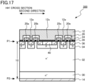
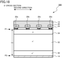
- the MOSFET 100 includes a silicon carbide layer 10, a source electrode 12 (first electrode), a drain electrode 14 (second electrode), a gate electrode pad 16, a metal wiring line 18, a first gate electrode 20a, a second gate electrode 20b, a third gate electrode 20c, a fourth gate electrode 20d, a fifth gate electrode 20e, a sixth gate electrode 20f, a gate wiring line 22, a gate insulating layer 24, an interlayer insulating layer 26, a field insulating layer 27, and a silicide layer 28.
- the source electrode 12 has a first portion 12a and a second portion 12b.
- the interlayer insulating layer 26 has a contact hole 26a.
- the first gate electrode 20a, the second gate electrode 20b, the third gate electrode 20c, the fourth gate electrode 20d, the fifth gate electrode 20e, and the sixth gate electrode 20f may be simply referred to collectively as a gate electrode 20.
- the silicon carbide layer 10 includes an n + -type drain region 30, an n - -type drift region 32 (first silicon carbide region), a p-type body region 34 (second silicon carbide region), an n-type source region 36 (third silicon carbide region), and a p-type body contact region 40.
- the silicon carbide layer 10 is provided between the source electrode 12 and the drain electrode 14.
- the silicon carbide layer 10 is a single crystal SiC.
- the silicon carbide layer 10 is, for example, 4H-SiC.
- the first face P1 is, for example, a face inclined by an angle equal to or more than 0° and equal to or less than 8° with respect to the (0001) face.
- the second face P2 is, for example, a face inclined by an angle equal to or more than 0° and equal to or less than 8° with respect to the (000-1) face.
- the (0001) face is referred to as a silicon face.
- the (000-1) face is referred to as a carbon face.
- the n + -type drain region 30 is provided on the side of the second face P2 in the silicon carbide layer 10.
- the drain region 30 contains, for example, nitrogen (N) as an n-type impurity.
- the n-type impurity concentration in the drain region 30 is, for example, equal to or more than 1 ⁇ 10 18 cm -3 and equal to or less than 1 ⁇ 10 21 cm -3 .
- the drain region 30 is electrically connected to the drain electrode 14.
- the drift region 32 contains, for example, nitrogen (N) as an n-type impurity.
- the n-type impurity concentration in the drift region 32 is lower than the n-type impurity concentration in the drain region 30.
- the n-type impurity concentration in the drift region 32 is, for example, equal to or more than 4 ⁇ 10 14 cm -3 and equal to or less than 1 ⁇ 10 17 cm -3 .
- the thickness of the drift region 32 is, for example, equal to or more than 4 ⁇ m and equal to or less than 150 ⁇ m.
- the p-type body region 34 is provided between the source electrode 12 and the drift region 32.
- the body region 34 is provided between the drift region 32 and the first face P1.
- the body region 34 functions as a channel region of the MOSFET 100.
- the body region 34 contains, for example, aluminum (Al) as a p-type impurity.
- the p-type impurity concentration in the body region 34 is, for example, equal to or more than 1 ⁇ 10 17 cm -3 and equal to or less than 5 ⁇ 10 18 cm -3 .
- the body region 34 is electrically connected to the source electrode 12.
- the electric potential of the body region 34 is fixed to the electric potential of the source electrode 12.
- the source region 36 contains, for example, phosphorus (P) as an n-type impurity.
- the n-type impurity concentration in the source region 36 is higher than the n-type impurity concentration in the drift region 32.
- the source region 36 is electrically connected to the source electrode 12.
- the electric potential of the source region 36 is fixed to the electric potential of the source electrode 12.
- the body contact region 40 contains, for example, aluminum (Al) as a p-type impurity.
- the p-type impurity concentration in the body contact region 40 is, for example, equal to or more than 5 ⁇ 10 18 cm -3 and equal to or less than 1 ⁇ 10 21 cm -3 .
- the fourth gate electrode 20d is provided between the source electrode 12 and the silicon carbide layer 10.
- the fourth gate electrode 20d is provided on the first face P1 side of the silicon carbide layer 10.
- the fourth gate electrode 20d extends in the first direction.
- the fourth gate electrode 20d is adjacent to the first gate electrode 20a.
- the fifth gate electrode 20e is provided between the source electrode 12 and the silicon carbide layer 10.
- the fifth gate electrode 20e is provided on the first face P1 side of the silicon carbide layer 10.
- the fifth gate electrode 20e extends in the first direction.
- the fifth gate electrode 20e is adjacent to the third gate electrode 20c.
- the sixth gate electrode 20f is provided between the source electrode 12 and the silicon carbide layer 10.
- the sixth gate electrode 20f is provided on the first face P1 side of the silicon carbide layer 10.
- the sixth gate electrode 20f extends in the first direction.
- the sixth gate electrode 20f is adjacent to the fourth gate electrode 20d.
- the gate electrode 20 is a conductive layer.
- the gate electrode 20 is, for example, polycrystalline silicon containing p-type impurities or n-type impurities.
- the body region 34 facing the gate electrode 20 functions as a channel region of the MOSFET 100.
- the gate wiring line 22 is provided between the source electrode 12 and the silicon carbide layer 10.
- the gate wiring line 22 is provided on the first face P1 side of the silicon carbide layer 10.
- a part of the gate wiring line 22 is provided between the source electrode 12 and the field insulating layer 27.
- the gate wiring line 22 extends in a second direction crossing the first direction.
- the gate wiring line 22 extends, for example, in a second direction perpendicular to the first direction.
- the gate electrode 20 is connected to the gate wiring line 22. According to the present invention, the first gate electrode 20a, the second gate electrode 20b, and the third gate electrode 20c are connected to the gate wiring line 22.
- the gate wiring line 22 is a conductive layer.
- the gate wiring line 22 is, for example, polycrystalline silicon containing p-type impurities or n-type impurities.
- the gate wiring line 22 is formed of, for example, the same material as the gate electrode 20.
- the gate wiring line 22 is, for example, a polycrystalline layer continuous with the gate electrode 20.
- the gate wiring line 22 is, for example, a polycrystalline silicon layer continuous with the gate electrode 20.
- the gate wiring line 22 and the gate electrode 20 are simultaneously formed, for example, by patterning the formed conductive film.
- a connection portion between the gate electrode 20 and the gate wiring line 22 is provided between the source electrode 12 and the silicon carbide layer 10.
- a connection portion between the first gate electrode 20a and the gate wiring line 22 and a connection portion between the second gate electrode 20b and the gate wiring line 22 are provided between the source electrode 12 and the silicon carbide layer 10.
- the distance between the first gate electrode 20a and the second gate electrode 20b in the second direction in a first region R1 is defined as S1.
- the distance between the first gate electrode 20a and the second gate electrode 20b in the second direction in a second region R2 closer to the gate wiring line 22 than the first region R1 is defined as S2.
- the distance between the second gate electrode 20b and the third gate electrode 20c in the second direction in the first region R1 is defined as S3.
- the distance between the second gate electrode 20b and the third gate electrode 20c in the second direction in the second region R2 is defined as S4.
- the MOSFET 100 satisfies the following Expression 1, Expression 2, and Expression 3.
- the MOSFET 100 satisfies, for example, the following Expression 4.
- the MOSFET 100 satisfies, for example, the following Expression 5.
- the MOSFET 100 satisfies, for example, the following Expression 6. 0.8 ⁇ S 2 ⁇ S 4 ⁇ 1.2 ⁇ S 2
- the MOSFET 100 satisfies, for example, the following Expression 7. 2 ⁇ S 1 ⁇ S 3
- MOSFET 100 satisfies, for example, the following Expression 8.
- S 1 + S 3 S 2 + S 4
- the width of the gate electrode 20 in the second direction is, for example, equal to or more than 1 ⁇ m and equal to or less than 3 ⁇ m.
- the gate insulating layer 24 is provided between the gate electrode 20 and the silicon carbide layer 10.
- the gate insulating layer 24 is provided, for example, between the first gate electrode 20a and the silicon carbide layer 10.
- the gate insulating layer 24 is provided, for example, between the second gate electrode 20b and the silicon carbide layer 10.
- the interlayer insulating layer 26 contains, for example, silicon oxide.
- the interlayer insulating layer 26 is, for example, silicon oxide.
- the interlayer insulating layer 26 is, for example, a deposited film formed by a vapor phase growth method.
Landscapes
- Electrodes Of Semiconductors (AREA)
- Internal Circuitry In Semiconductor Integrated Circuit Devices (AREA)
- Metal-Oxide And Bipolar Metal-Oxide Semiconductor Integrated Circuits (AREA)
Claims (9)
- Halbleitervorrichtung (100, 200, 300), umfassend:eine erste Elektrode (12);eine zweite Elektrode (14);eine Siliziumkarbidschicht (10), die zwischen der ersten Elektrode (12) und der zweiten Elektrode (14) vorgesehen ist und eine ersten Siliziumkarbidregion (32) eines ersten Leitfähigkeitstyps, eine zweite Siliziumkarbidregion (34) eines zweiten Leitfähigkeitstyps, die zwischen der ersten Elektrode (12) und der ersten Siliziumkarbidregion (32) vorgesehen ist, und eine dritte Siliziumkarbidregion (36) des ersten Leitfähigkeitstyps, die zwischen der ersten Elektrode (12) und der zweiten Siliziumkarbidregion (34) vorgesehen ist, umfasst;eine erste Gate-Elektrode (20a), die zwischen der ersten Elektrode (12) und der Siliziumkarbidschicht (10) vorgesehen ist und sich in einer ersten Richtung parallel zu einer Oberfläche der Siliziumkarbidschicht (10) erstreckt;eine zweite Gate-Elektrode (20b), die zwischen der ersten Elektrode (12) und der Siliziumkarbidschicht (10) vorgesehen ist und sich in der ersten Richtung erstreckt;eine dritte Gate-Elektrode (20c), die zwischen der ersten Elektrode (12) und der Siliziumkarbidschicht (10) vorgesehen ist und sich in der ersten Richtung erstreckt;eine Gate-Verdrahtungsleitung (22), die zwischen der ersten Elektrode (12) und der Siliziumkarbidschicht (10) vorgesehen ist und sich in einer zweiten Richtung erstreckt, die die erste Richtung kreuzt, wobei die zweite Richtung parallel zur Oberfläche ist, wobei die erste Gate-Elektrode (20a), die zweite Gate-Elektrode (20b) und die dritte Gate-Elektrode (20c) mit der Gate-Verdrahtungsleitung (22) verbunden sind; undeine Gate-Isolierschicht (24), die zwischen der ersten Gate-Elektrode (20a) und der Siliziumkarbidschicht (10), zwischen der zweiten Gate-Elektrode (20b) und der Siliziumkarbidschicht (10) und zwischen der dritten Gate-Elektrode (20c) und der Siliziumkarbidschicht (10) vorgesehen ist,wobei unter der Annahme, dass ein Abstand zwischen der ersten Gate-Elektrode (20a) und der zweiten Gate-Elektrode (20b) in der zweiten Richtung in einer ersten Region (R1) S1 ist, ein Abstand zwischen der ersten Gate-Elektrode (20a) und der zweiten Gate-Elektrode (20b) in der zweiten Richtung in einem zweiten Bereich (R2), der näher an der Gate-Verdrahtungsleitung (22) liegt als die erste Region (R1), S2 ist, ein Abstand zwischen der zweiten Gate-Elektrode (20b) und der dritten Gate-Elektrode (20c) in der zweiten Richtung in der ersten Region (R1) S3 ist, und ein Abstand zwischen der zweiten Gate-Elektrode (20b) und der dritten Gate-Elektrode (20c) in der zweiten Richtung in dem zweiten Bereich (R2) S4 ist, nachdem Ausdruck 1, Ausdruck 2, Ausdruck 3 und Ausdruck 4 erfüllt sind, und die erste Gate-Elektrode (20a), die zweite Gate-Elektrode (20b) und die dritte Gate-Elektrode (20c) mit der Gate-Verdrahtungsleitung (22) in der zweiten Region (R2) verbunden sind,


- Halbleitervorrichtung (100, 200, 300) gemäß Anspruch 1, wobei der folgende Ausdruck 5 erfüllt ist,

- Halbleitervorrichtung (100, 200, 300) gemäß Anspruch 1, wobei der folgende Ausdruck 6 erfüllt ist,

- Halbleitervorrichtung (100, 200, 300) gemäß Anspruch 1, wobei der folgende Ausdruck 7 erfüllt ist,

- Halbleitervorrichtung (100, 300) gemäß Anspruch 1, wobei der folgende Ausdruck 8 erfüllt ist,

- Halbleitervorrichtung (100, 200, 300) gemäß Anspruch 1, ferner umfassend:
eine Isolierschicht (26), die zwischen der ersten Gate-Elektrode (20a) und der ersten Elektrode (12), zwischen der zweiten Gate-Elektrode (20b) und der ersten Elektrode (12) und zwischen der Gate-Verdrahtungsleitung (22) und der ersten Elektrode (12) vorgesehen ist. - Halbleitervorrichtung (100, 200, 300) nach Anspruch 1,wobei die erste Elektrode (12) einen ersten Abschnitt (12a) und einen zweiten Abschnitt (12b) aufweist,der erste Abschnitt (12a) zwischen der ersten Gate-Elektrode (20a) und der zweiten Gate-Elektrode (20b) angeordnet ist, und der zweite Abschnitt (12b) zwischen der zweiten Gate-Elektrode (20b) und der dritten Gate-Elektrode (20c) angeordnet ist und der zweite Abschnitt (12b) in Kontakt mit dem ersten Siliziumkarbidbereich (32) steht.
- Halbleitervorrichtung (200) nach Anspruch 1, ferner umfassend:eine vierte Gate-Elektrode (20d), die zwischen der ersten Elektrode (12) und der Siliziumkarbidschicht (10) vorgesehen ist und sich in der ersten Richtung erstreckt, wobei die erste Gate-Elektrode (20a) zwischen der zweiten Gate-Elektrode (20b) und der vierten Gate-Elektrode (20d) angeordnet ist,wobei, unter der Annahme, dass ein Abstand zwischen der vierten Gate-Elektrode (20d) und der ersten Gate-Elektrode (20a) in der zweiten Richtung in der ersten Region (R1) S5 ist und ein Abstand zwischen der vierten Gate-Elektrode (20d) und der ersten Gate-Elektrode (20a) in der zweiten Richtung in der zweiten Region (R2) S6 ist, die folgenden Ausdrücke 9 und 10 erfüllt sind,


- Halbleitervorrichtung (200) gemäß Anspruch 8, wobei der folgende Ausdruck 11 erfüllt ist,

Applications Claiming Priority (1)
| Application Number | Priority Date | Filing Date | Title |
|---|---|---|---|
| JP2020207693A JP7516236B2 (ja) | 2020-12-15 | 2020-12-15 | 半導体装置 |
Publications (2)
| Publication Number | Publication Date |
|---|---|
| EP4016641A1 EP4016641A1 (de) | 2022-06-22 |
| EP4016641B1 true EP4016641B1 (de) | 2025-07-09 |
Family
ID=77411608
Family Applications (1)
| Application Number | Title | Priority Date | Filing Date |
|---|---|---|---|
| EP21192097.0A Active EP4016641B1 (de) | 2020-12-15 | 2021-08-19 | Halbleiterbauelement und layout für gate-elektroden |
Country Status (4)
| Country | Link |
|---|---|
| US (1) | US11769800B2 (de) |
| EP (1) | EP4016641B1 (de) |
| JP (1) | JP7516236B2 (de) |
| CN (1) | CN114639733B (de) |
Families Citing this family (3)
| Publication number | Priority date | Publication date | Assignee | Title |
|---|---|---|---|---|
| JP7513565B2 (ja) * | 2021-04-14 | 2024-07-09 | 株式会社デンソー | スイッチング素子の製造方法 |
| JP7574162B2 (ja) * | 2021-09-22 | 2024-10-28 | 東芝デバイス&ストレージ株式会社 | 半導体装置 |
| JP2024137537A (ja) * | 2023-03-24 | 2024-10-07 | 株式会社東芝 | 半導体装置 |
Family Cites Families (19)
| Publication number | Priority date | Publication date | Assignee | Title |
|---|---|---|---|---|
| US7345342B2 (en) * | 2001-01-30 | 2008-03-18 | Fairchild Semiconductor Corporation | Power semiconductor devices and methods of manufacture |
| JP2003197910A (ja) | 2001-12-26 | 2003-07-11 | Toshiba Corp | 半導体装置 |
| US7075147B2 (en) * | 2003-06-11 | 2006-07-11 | International Rectifier Corporation | Low on resistance power MOSFET with variably spaced trenches and offset contacts |
| JP2005333068A (ja) * | 2004-05-21 | 2005-12-02 | Toshiba Corp | 半導体装置 |
| KR100674956B1 (ko) * | 2005-02-12 | 2007-01-26 | 삼성전자주식회사 | Esd에 내성을 가지는 프리미티브 셀 |
| JP5211666B2 (ja) | 2007-12-06 | 2013-06-12 | 株式会社デンソー | 絶縁ゲートトランジスタ |
| US8080847B2 (en) * | 2008-04-08 | 2011-12-20 | Fairchild Semiconductor Corporation | Low on resistance CMOS “wave” transistor for integrated circuit applications |
| JP2010206002A (ja) * | 2009-03-04 | 2010-09-16 | Fuji Electric Systems Co Ltd | pチャネル型炭化珪素MOSFET |
| JP5493840B2 (ja) | 2009-12-25 | 2014-05-14 | 富士電機株式会社 | 半導体装置 |
| JP5667926B2 (ja) * | 2011-05-12 | 2015-02-12 | 新電元工業株式会社 | 半導体素子 |
| JP5992094B2 (ja) | 2013-04-03 | 2016-09-14 | 三菱電機株式会社 | 半導体装置 |
| JP6541862B2 (ja) | 2013-08-28 | 2019-07-10 | ローム株式会社 | 半導体装置 |
| US9716168B2 (en) * | 2014-09-24 | 2017-07-25 | Shindengen Electric Manufacturing Co., Ltd. | Silicon carbide semiconductor device, method of manufacturing silicon carbide semiconductor device and method of designing silicon carbide semiconductor device |
| JP2017135245A (ja) | 2016-01-27 | 2017-08-03 | 株式会社東芝 | 半導体装置 |
| WO2019077877A1 (ja) * | 2017-10-17 | 2019-04-25 | 富士電機株式会社 | 炭化珪素半導体装置および炭化珪素半導体装置の製造方法 |
| JP2018082202A (ja) | 2017-12-27 | 2018-05-24 | ルネサスエレクトロニクス株式会社 | 半導体装置 |
| JP6966377B2 (ja) | 2018-04-19 | 2021-11-17 | ルネサスエレクトロニクス株式会社 | 半導体装置およびその製造方法 |
| KR102563442B1 (ko) * | 2018-12-07 | 2023-08-03 | 현대자동차 주식회사 | 반도체 소자 |
| JP2020074426A (ja) | 2020-01-10 | 2020-05-14 | 株式会社東芝 | 半導体装置 |
-
2020
- 2020-12-15 JP JP2020207693A patent/JP7516236B2/ja active Active
-
2021
- 2021-06-11 CN CN202110651477.6A patent/CN114639733B/zh active Active
- 2021-08-19 EP EP21192097.0A patent/EP4016641B1/de active Active
- 2021-09-01 US US17/464,604 patent/US11769800B2/en active Active
Also Published As
| Publication number | Publication date |
|---|---|
| US20220190118A1 (en) | 2022-06-16 |
| JP7516236B2 (ja) | 2024-07-16 |
| EP4016641A1 (de) | 2022-06-22 |
| US11769800B2 (en) | 2023-09-26 |
| JP2022094676A (ja) | 2022-06-27 |
| CN114639733B (zh) | 2024-10-29 |
| CN114639733A (zh) | 2022-06-17 |
Similar Documents
| Publication | Publication Date | Title |
|---|---|---|
| US11411084B2 (en) | Semiconductor device, inverter circuit, drive device, vehicle, and elevator | |
| US10930773B2 (en) | Semiconductor device | |
| JP6649183B2 (ja) | 半導体装置 | |
| JP7003019B2 (ja) | 半導体装置 | |
| US10872974B2 (en) | Semiconductor device | |
| US11222973B2 (en) | Semiconductor device | |
| US11955543B2 (en) | Semiconductor device | |
| EP4016641B1 (de) | Halbleiterbauelement und layout für gate-elektroden | |
| US12382711B2 (en) | Semiconductor device | |
| US12107127B2 (en) | Semiconductor device | |
| US12363929B2 (en) | Semiconductor device | |
| JP2022009745A (ja) | 半導体装置 | |
| JP2020074426A (ja) | 半導体装置 | |
| JP2025113483A (ja) | 半導体装置 | |
| US12255253B2 (en) | Semiconductor device | |
| EP4156301A1 (de) | Halbleiterbauelement | |
| US20260040658A1 (en) | Semiconductor device | |
| US20260090072A1 (en) | Semiconductor device | |
| US12237411B2 (en) | Semiconductor device | |
| US20240321968A1 (en) | Semiconductor device | |
| CN121014272A (zh) | 半导体装置 |
Legal Events
| Date | Code | Title | Description |
|---|---|---|---|
| PUAI | Public reference made under article 153(3) epc to a published international application that has entered the european phase |
Free format text: ORIGINAL CODE: 0009012 |
|
| STAA | Information on the status of an ep patent application or granted ep patent |
Free format text: STATUS: REQUEST FOR EXAMINATION WAS MADE |
|
| 17P | Request for examination filed |
Effective date: 20210819 |
|
| AK | Designated contracting states |
Kind code of ref document: A1 Designated state(s): AL AT BE BG CH CY CZ DE DK EE ES FI FR GB GR HR HU IE IS IT LI LT LU LV MC MK MT NL NO PL PT RO RS SE SI SK SM TR |
|
| REG | Reference to a national code |
Ref country code: DE Ref legal event code: R079 Ref document number: 602021033663 Country of ref document: DE Free format text: PREVIOUS MAIN CLASS: H01L0029423000 Ipc: H10D0030660000 |
|
| GRAP | Despatch of communication of intention to grant a patent |
Free format text: ORIGINAL CODE: EPIDOSNIGR1 |
|
| STAA | Information on the status of an ep patent application or granted ep patent |
Free format text: STATUS: GRANT OF PATENT IS INTENDED |
|
| RIC1 | Information provided on ipc code assigned before grant |
Ipc: H10D 84/00 20250101ALI20250123BHEP Ipc: H10D 64/27 20250101ALI20250123BHEP Ipc: H10D 62/832 20250101ALI20250123BHEP Ipc: H10D 30/66 20250101AFI20250123BHEP |
|
| INTG | Intention to grant announced |
Effective date: 20250204 |
|
| GRAS | Grant fee paid |
Free format text: ORIGINAL CODE: EPIDOSNIGR3 |
|
| GRAA | (expected) grant |
Free format text: ORIGINAL CODE: 0009210 |
|
| STAA | Information on the status of an ep patent application or granted ep patent |
Free format text: STATUS: THE PATENT HAS BEEN GRANTED |
|
| AK | Designated contracting states |
Kind code of ref document: B1 Designated state(s): AL AT BE BG CH CY CZ DE DK EE ES FI FR GB GR HR HU IE IS IT LI LT LU LV MC MK MT NL NO PL PT RO RS SE SI SK SM TR |
|
| REG | Reference to a national code |
Ref country code: GB Ref legal event code: FG4D |
|
| REG | Reference to a national code |
Ref country code: CH Ref legal event code: EP |
|
| REG | Reference to a national code |
Ref country code: IE Ref legal event code: FG4D |
|
| REG | Reference to a national code |
Ref country code: DE Ref legal event code: R096 Ref document number: 602021033663 Country of ref document: DE |
|
| PGFP | Annual fee paid to national office [announced via postgrant information from national office to epo] |
Ref country code: DE Payment date: 20250716 Year of fee payment: 5 |
|
| PGFP | Annual fee paid to national office [announced via postgrant information from national office to epo] |
Ref country code: GB Payment date: 20250717 Year of fee payment: 5 |
|
| PGFP | Annual fee paid to national office [announced via postgrant information from national office to epo] |
Ref country code: AT Payment date: 20251020 Year of fee payment: 5 Ref country code: FR Payment date: 20250721 Year of fee payment: 5 |
|
| REG | Reference to a national code |
Ref country code: NL Ref legal event code: MP Effective date: 20250709 |
|
| PG25 | Lapsed in a contracting state [announced via postgrant information from national office to epo] |
Ref country code: PT Free format text: LAPSE BECAUSE OF FAILURE TO SUBMIT A TRANSLATION OF THE DESCRIPTION OR TO PAY THE FEE WITHIN THE PRESCRIBED TIME-LIMIT Effective date: 20251110 |
|
| PG25 | Lapsed in a contracting state [announced via postgrant information from national office to epo] |
Ref country code: NL Free format text: LAPSE BECAUSE OF FAILURE TO SUBMIT A TRANSLATION OF THE DESCRIPTION OR TO PAY THE FEE WITHIN THE PRESCRIBED TIME-LIMIT Effective date: 20250709 |
|
| REG | Reference to a national code |
Ref country code: AT Ref legal event code: MK05 Ref document number: 1813115 Country of ref document: AT Kind code of ref document: T Effective date: 20250709 |
|
| PG25 | Lapsed in a contracting state [announced via postgrant information from national office to epo] |
Ref country code: IS Free format text: LAPSE BECAUSE OF FAILURE TO SUBMIT A TRANSLATION OF THE DESCRIPTION OR TO PAY THE FEE WITHIN THE PRESCRIBED TIME-LIMIT Effective date: 20251109 |
|
| PG25 | Lapsed in a contracting state [announced via postgrant information from national office to epo] |
Ref country code: NO Free format text: LAPSE BECAUSE OF FAILURE TO SUBMIT A TRANSLATION OF THE DESCRIPTION OR TO PAY THE FEE WITHIN THE PRESCRIBED TIME-LIMIT Effective date: 20251009 |
|
| REG | Reference to a national code |
Ref country code: LT Ref legal event code: MG9D |
|
| PG25 | Lapsed in a contracting state [announced via postgrant information from national office to epo] |
Ref country code: AT Free format text: LAPSE BECAUSE OF FAILURE TO SUBMIT A TRANSLATION OF THE DESCRIPTION OR TO PAY THE FEE WITHIN THE PRESCRIBED TIME-LIMIT Effective date: 20250709 |
|
| PG25 | Lapsed in a contracting state [announced via postgrant information from national office to epo] |
Ref country code: FI Free format text: LAPSE BECAUSE OF FAILURE TO SUBMIT A TRANSLATION OF THE DESCRIPTION OR TO PAY THE FEE WITHIN THE PRESCRIBED TIME-LIMIT Effective date: 20250709 |
|
| PG25 | Lapsed in a contracting state [announced via postgrant information from national office to epo] |
Ref country code: HR Free format text: LAPSE BECAUSE OF FAILURE TO SUBMIT A TRANSLATION OF THE DESCRIPTION OR TO PAY THE FEE WITHIN THE PRESCRIBED TIME-LIMIT Effective date: 20250709 |
|
| PG25 | Lapsed in a contracting state [announced via postgrant information from national office to epo] |
Ref country code: GR Free format text: LAPSE BECAUSE OF FAILURE TO SUBMIT A TRANSLATION OF THE DESCRIPTION OR TO PAY THE FEE WITHIN THE PRESCRIBED TIME-LIMIT Effective date: 20251010 |
|
| PG25 | Lapsed in a contracting state [announced via postgrant information from national office to epo] |
Ref country code: SE Free format text: LAPSE BECAUSE OF FAILURE TO SUBMIT A TRANSLATION OF THE DESCRIPTION OR TO PAY THE FEE WITHIN THE PRESCRIBED TIME-LIMIT Effective date: 20250709 |
|
| PG25 | Lapsed in a contracting state [announced via postgrant information from national office to epo] |
Ref country code: LV Free format text: LAPSE BECAUSE OF FAILURE TO SUBMIT A TRANSLATION OF THE DESCRIPTION OR TO PAY THE FEE WITHIN THE PRESCRIBED TIME-LIMIT Effective date: 20250709 |
|
| PG25 | Lapsed in a contracting state [announced via postgrant information from national office to epo] |
Ref country code: BG Free format text: LAPSE BECAUSE OF FAILURE TO SUBMIT A TRANSLATION OF THE DESCRIPTION OR TO PAY THE FEE WITHIN THE PRESCRIBED TIME-LIMIT Effective date: 20250709 Ref country code: PL Free format text: LAPSE BECAUSE OF FAILURE TO SUBMIT A TRANSLATION OF THE DESCRIPTION OR TO PAY THE FEE WITHIN THE PRESCRIBED TIME-LIMIT Effective date: 20250709 |
|
| PG25 | Lapsed in a contracting state [announced via postgrant information from national office to epo] |
Ref country code: RS Free format text: LAPSE BECAUSE OF FAILURE TO SUBMIT A TRANSLATION OF THE DESCRIPTION OR TO PAY THE FEE WITHIN THE PRESCRIBED TIME-LIMIT Effective date: 20251009 |
|
| PG25 | Lapsed in a contracting state [announced via postgrant information from national office to epo] |
Ref country code: ES Free format text: LAPSE BECAUSE OF FAILURE TO SUBMIT A TRANSLATION OF THE DESCRIPTION OR TO PAY THE FEE WITHIN THE PRESCRIBED TIME-LIMIT Effective date: 20250709 |
|
| PG25 | Lapsed in a contracting state [announced via postgrant information from national office to epo] |
Ref country code: RO Free format text: LAPSE BECAUSE OF FAILURE TO SUBMIT A TRANSLATION OF THE DESCRIPTION OR TO PAY THE FEE WITHIN THE PRESCRIBED TIME-LIMIT Effective date: 20250709 |
|
| REG | Reference to a national code |
Ref country code: CH Ref legal event code: H13 Free format text: ST27 STATUS EVENT CODE: U-0-0-H10-H13 (AS PROVIDED BY THE NATIONAL OFFICE) Effective date: 20260324 |
|
| PG25 | Lapsed in a contracting state [announced via postgrant information from national office to epo] |
Ref country code: SM Free format text: LAPSE BECAUSE OF FAILURE TO SUBMIT A TRANSLATION OF THE DESCRIPTION OR TO PAY THE FEE WITHIN THE PRESCRIBED TIME-LIMIT Effective date: 20250709 |
|
| PG25 | Lapsed in a contracting state [announced via postgrant information from national office to epo] |
Ref country code: DK Free format text: LAPSE BECAUSE OF FAILURE TO SUBMIT A TRANSLATION OF THE DESCRIPTION OR TO PAY THE FEE WITHIN THE PRESCRIBED TIME-LIMIT Effective date: 20250709 |
|
| PG25 | Lapsed in a contracting state [announced via postgrant information from national office to epo] |
Ref country code: IT Free format text: LAPSE BECAUSE OF FAILURE TO SUBMIT A TRANSLATION OF THE DESCRIPTION OR TO PAY THE FEE WITHIN THE PRESCRIBED TIME-LIMIT Effective date: 20250709 Ref country code: LU Free format text: LAPSE BECAUSE OF NON-PAYMENT OF DUE FEES Effective date: 20250819 |
|
| PG25 | Lapsed in a contracting state [announced via postgrant information from national office to epo] |
Ref country code: CH Free format text: LAPSE BECAUSE OF NON-PAYMENT OF DUE FEES Effective date: 20250831 Ref country code: CZ Free format text: LAPSE BECAUSE OF FAILURE TO SUBMIT A TRANSLATION OF THE DESCRIPTION OR TO PAY THE FEE WITHIN THE PRESCRIBED TIME-LIMIT Effective date: 20250709 |
|
| PG25 | Lapsed in a contracting state [announced via postgrant information from national office to epo] |
Ref country code: EE Free format text: LAPSE BECAUSE OF FAILURE TO SUBMIT A TRANSLATION OF THE DESCRIPTION OR TO PAY THE FEE WITHIN THE PRESCRIBED TIME-LIMIT Effective date: 20250709 Ref country code: SK Free format text: LAPSE BECAUSE OF FAILURE TO SUBMIT A TRANSLATION OF THE DESCRIPTION OR TO PAY THE FEE WITHIN THE PRESCRIBED TIME-LIMIT Effective date: 20250709 |