EP4012787B1 - Thermoelektrisches umwandlungselement - Google Patents
Thermoelektrisches umwandlungselement Download PDFInfo
- Publication number
- EP4012787B1 EP4012787B1 EP20849156.3A EP20849156A EP4012787B1 EP 4012787 B1 EP4012787 B1 EP 4012787B1 EP 20849156 A EP20849156 A EP 20849156A EP 4012787 B1 EP4012787 B1 EP 4012787B1
- Authority
- EP
- European Patent Office
- Prior art keywords
- thermoelectric conversion
- thermal conduction
- conduction portion
- electrode
- high thermal
- Prior art date
- Legal status (The legal status is an assumption and is not a legal conclusion. Google has not performed a legal analysis and makes no representation as to the accuracy of the status listed.)
- Active
Links
Images



Classifications
-
- H—ELECTRICITY
- H10—SEMICONDUCTOR DEVICES; ELECTRIC SOLID-STATE DEVICES NOT OTHERWISE PROVIDED FOR
- H10N—ELECTRIC SOLID-STATE DEVICES NOT OTHERWISE PROVIDED FOR
- H10N10/00—Thermoelectric devices comprising a junction of dissimilar materials, i.e. devices exhibiting Seebeck or Peltier effects
- H10N10/10—Thermoelectric devices comprising a junction of dissimilar materials, i.e. devices exhibiting Seebeck or Peltier effects operating with only the Peltier or Seebeck effects
- H10N10/17—Thermoelectric devices comprising a junction of dissimilar materials, i.e. devices exhibiting Seebeck or Peltier effects operating with only the Peltier or Seebeck effects characterised by the structure or configuration of the cell or thermocouple forming the device
-
- H—ELECTRICITY
- H10—SEMICONDUCTOR DEVICES; ELECTRIC SOLID-STATE DEVICES NOT OTHERWISE PROVIDED FOR
- H10N—ELECTRIC SOLID-STATE DEVICES NOT OTHERWISE PROVIDED FOR
- H10N10/00—Thermoelectric devices comprising a junction of dissimilar materials, i.e. devices exhibiting Seebeck or Peltier effects
- H10N10/10—Thermoelectric devices comprising a junction of dissimilar materials, i.e. devices exhibiting Seebeck or Peltier effects operating with only the Peltier or Seebeck effects
- H10N10/13—Thermoelectric devices comprising a junction of dissimilar materials, i.e. devices exhibiting Seebeck or Peltier effects operating with only the Peltier or Seebeck effects characterised by the heat-exchanging means at the junction
-
- H—ELECTRICITY
- H10—SEMICONDUCTOR DEVICES; ELECTRIC SOLID-STATE DEVICES NOT OTHERWISE PROVIDED FOR
- H10N—ELECTRIC SOLID-STATE DEVICES NOT OTHERWISE PROVIDED FOR
- H10N10/00—Thermoelectric devices comprising a junction of dissimilar materials, i.e. devices exhibiting Seebeck or Peltier effects
- H10N10/80—Constructional details
- H10N10/82—Interconnections
-
- H—ELECTRICITY
- H10—SEMICONDUCTOR DEVICES; ELECTRIC SOLID-STATE DEVICES NOT OTHERWISE PROVIDED FOR
- H10N—ELECTRIC SOLID-STATE DEVICES NOT OTHERWISE PROVIDED FOR
- H10N10/00—Thermoelectric devices comprising a junction of dissimilar materials, i.e. devices exhibiting Seebeck or Peltier effects
- H10N10/80—Constructional details
Definitions
- thermoelectric conversion element The present disclosure relates to a thermoelectric conversion element.
- thermoelectric conversion element may be used to perform power generation using geothermal heat, exhaust heat of a factory, or the like.
- JP 4,895,293 B2 discloses an embodiment in which a flexible substrate having a pattern layer and composed of a resin layer and a metal layer is provided on both surfaces of a thermoelectric conversion module having a P-type thermoelectric element material and an N-type thermoelectric element material.
- a metal layer included in one flexible substrate overlaps one electrode included in the thermoelectric conversion module, and a metal layer included in the other flexible substrate overlaps the other electrode included in the thermoelectric conversion module.
- thermoelectric conversion module by setting one flexible substrate to a high temperature state and setting the other flexible substrate to a low temperature state, a temperature difference is generated in a planar direction of the thermoelectric conversion module. Accordingly, an electromotive force is generated in the thermoelectric conversion module.
- EP 3 035 397 A1 discloses a thermally conductive adhesive sheet comprising a base material comprising a high thermally conductive portion and a low thermally conductive portion; and an adhesive layer, wherein the adhesive layer is laminated on one face of the base material, and the other face of the base material is composed of a face of the low thermally conductive portion opposite to a face in contact with the adhesive layer and a face of the high thermally conductive portion opposite to a face in contact with the adhesive layer, or at least either the high thermally conductive portion or the low thermally conductive portion constitutes a portion of a thickness of the base material, and a method for producing the thermally conductive adhesive sheet, and an electronic device using the thermally conductive adhesive sheet.
- thermoelectric conversion module comprising: a film-type thermoelectric conversion element body having p-type thermoelectric conversion elements and n-type thermoelectric conversion elements joined in one direction in a plane; and heat conductors joined to where the p-type thermoelectric conversion elements and the n-type thermoelectric conversion elements are joined on one surface of the thermoelectric conversion element body. Insulation regions are disposed adjoining both sides of the heat conductors in said one direction and, if disposed on the heat source, have radiation reflecting bodies and/or radiation prevention bodies closer to the heat source than the thermoelectric conversion element body.
- thermoelectric conversion element as described above, further improvement in thermoelectric conversion efficiency is required. Therefore, an object of an aspect of the present disclosure is to provide a thermoelectric conversion element capable of improving thermoelectric conversion efficiency.
- thermoelectric conversion element according to the present invention is as follows.
- thermoelectric conversion element includes a substrate including a first main face and a second main face located on the opposite side of the first main face, a first electrode provided on the first main face, an n-type thermoelectric conversion layer electrically connected to the first electrode, a p-type thermoelectric conversion layer in contact with the n-type thermoelectric conversion layer, and a second electrode electrically connected to the p-type thermoelectric conversion layer, a sealing layer provided on the first main face, the sealing layer covering the first electrode, the n-type thermoelectric conversion layer, the p-type thermoelectric conversion layer, and the second electrode, and a first high thermal conduction portion, a second high thermal conduction portion, and a low thermal conduction portion provided only on the second main face, wherein the first electrode, the n-type thermoelectric conversion layer, the p-type thermoelectric conversion layer, and the second electrode are arranged in order along an alignment direction orthogonal to a thickness direction of the substrate, wherein the first electrode is overlapped with the first high thermal conduction portion in the
- the thermal conductivity of the low thermal conduction portion is 0.2W/mK or less.
- the thermal conductivity of the low thermal conduction portion is 0.08W/mK or less.
- thermoelectric conversion element of the present invention the thermal conductivity of the first high thermal conduction portion and a thermal conductivity of the second high thermal conduction portion are 5W/mK or more.
- thermoelectric conversion element of the present invention the thermal conductivity of the first electrode and a thermal conductivity of the second electrode are 5W/mK or more.
- the substrate has a flexibility.
- the interval from the first high thermal conduction portion to the contact portion along the alignment direction is greater than or equal to 5 times a length of the first high thermal conduction portion along the thickness direction, and an interval from the second high thermal conduction portion to the contact portion along the alignment direction is greater than or equal to 5 times a length of the second high thermal conduction portion along the thickness direction.
- thermoelectric conversion element capable of improving thermoelectric conversion efficiency
- FIG. 1 is a schematic cross-sectional view showing a thermoelectric conversion element according to the present embodiment.
- the thermoelectric conversion element 1 shown in FIG. 1 is an element capable of generating electric power by being supplied with heat from the outside.
- the thermoelectric conversion element 1 is, for example, an element that converts heat into electricity by using a temperature difference in the thermoelectric conversion element 20.
- the thermoelectric conversion element 1 is a so-called in-plane type element. Therefore, the thermoelectric conversion element 1 is likely to be more excellent in workability and flexibility than, for example, a ⁇ -type element (cross-plane type element).
- thermoelectric conversion element 1 can be provided along the side surface of a cylindrical pipe or the like used for recovering factory exhaust heat, for example. That is, the thermoelectric conversion element 1 can be easily disposed at various positions. Therefore, the thermoelectric conversion element 1 is used, for example, as a power source of a plant sensor using exhaust heat.
- the contact resistance between the thermoelectric conversion material included in the thermoelectric conversion element 1 and the electrode is likely to be lower than that of the ⁇ -type module. In the following, the temperature of each component of the thermoelectric conversion element 1 is measured under natural convection conditions of air.
- the thermoelectric conversion element 1 includes a thermoelectric conversion module 2 and a sheet member 3.
- the thermoelectric conversion module 2 is a thermoelectric conversion portion in the thermoelectric conversion element 1, and includes a substrate 11, a first electrode 12, a second electrode 13, an element portion 14, and a sealing layer 15.
- the substrate 11 is, for example, a sheet member made of a resin exhibiting heat resistance and flexibility, and has a substantially flat plate shape.
- the resin constituting the substrate 11 include a (meth) acrylic based resin, a (meth) acrylonitrile based resin, a polyamide based resin, a polycarbonate based resin, a polyether based resin, a polyester based resin, an epoxy based resin, an organosiloxane based resin, a polyimide based resin, and a polysulfone based resin.
- the thickness of the substrate 11 is, for example, 5 ⁇ m or more and 50 ⁇ m or less.
- the thermal conductivity of the substrate 11 is, for example, 0.1W/mK (corresponding to 0.1 watts per meter per Kelvin and 0.1W ⁇ m -1 ⁇ K -1 ) or more and 0.3W/mK or less.
- the substrate 11 has a first main face 11a and a second main face 11b located on the opposite side of the first main face 11a.
- the first main face 11a and the second main face 11b are faces intersecting the direction along the thickness of the substrate 11.
- the shapes of the first main face 11a and the second main face 11b are not particularly limited, and are, for example, polygonal, circular, elliptical, or the like.
- the direction along the thickness of the substrate 11 is simply referred to as a thickness direction D1.
- a view from the thickness direction D1 corresponds to a plan view.
- the first electrode 12 is a member constituting a terminal included in the thermoelectric conversion module 2, and is a conductor provided on the first main face 11a of the substrate 11.
- the first electrode 12 is a conductor made of, for example, a metal, an alloy, or a conductive resin.
- the first electrode 12 is formed on the substrate 11 by various dry methods, for example. Examples of the dry method include a physical vapor deposition method (PVD method) and patterning of a metal foil or an alloy foil.
- the first electrode 12 may be formed using a nano-paste or the like in which metal particles are dispersed.
- the shape of the first electrode 12 in a plan view is not particularly limited, and is, for example, a polygonal shape, a circular shape, an elliptical shape, or the like.
- the thickness of the first electrode 12 is, for example, 6 ⁇ m or more and 70 ⁇ m or less.
- the thermal conductivity of the first electrode 12 is, for example, 5W/mK or more. In this case, the first electrode 12 is likely to be easily heated from the outside.
- the thermal conductivity of the first electrode 12 may be, for example, 30W/mK or more.
- the second electrode 13 is a member constituting a terminal included in the thermoelectric conversion module 2 similarly to the first electrode 12, and is a conductor provided on the first main face 11a of the substrate 11.
- the second electrode 13 is separated from the first electrode 12.
- the second electrode 13 is formed at the same time as the first electrode 12. Therefore, the second electrode 13 is made of the same material as the first electrode 12.
- the shape of the second electrode 13 in a plan view is not particularly limited, and is, for example, a polygonal shape, a circular shape, an elliptical shape, or the like.
- the thermal conductivity of the second electrode 13 is, for example, 5W/mK or more.
- the thermal conductivity of the second electrode 13 may be, for example, 30W/mK or more.
- the element portion 14 is a member in which thermoelectric conversion is performed in the thermoelectric conversion module 2.
- the shape of the element portion 14 in a plan view is not particularly limited, and is, for example, a polygonal shape, a circular shape, an elliptical shape, or the like.
- the element portion 14 includes an n-type thermoelectric conversion layer 14a and a p-type thermoelectric conversion layer 14b. In the present embodiment, the n-type thermoelectric conversion layer 14a and the p-type thermoelectric conversion layer 14b have the same shape.
- the n-type thermoelectric conversion layer 14a is disposed on the first main face 11a of the substrate 11 and electrically connected to the first electrode 12. In this embodiment, the n-type thermoelectric conversion layer 14a is located between the first electrode 12 and the second electrode 13 and is in contact with the first electrode 12. The n-type thermoelectric conversion layer 14a covers a part of the first electrode 12.
- the n-type thermoelectric conversion layer 14a is, for example, an n-type semiconductor layer.
- the n-type thermoelectric conversion layer 14a includes, for example, a composite of an inorganic substance and an organic substance or a composite of a plurality of organic substances.
- the inorganic substance examples include titanium disulfide (TiS 2 ), bismuth tellurium (Bi 2 Te 3 ), skutterudite, and nickel (Ni).
- the inorganic substance may be titanium disulfide (TiS 2 ).
- the organic substance examples include an n-type single-walled carbon nanotube (SWCNT) and tetrathiafulvalene-tetracyanoquinodimethane (TTF-TCNQ).
- the n-type thermoelectric conversion layer 14a is formed by various dry methods or wet methods, for example. Examples of the wet method include a doctor blade method, a dip coating method, a spray coating method, a spin coating method, and an inkjet method.
- the thickness of the n-type thermoelectric conversion layer 14a is, for example, 9 ⁇ m or more and 200 ⁇ m or less.
- the thermal conductivity of the n-type thermoelectric conversion layer 14a is, for example, 0.01W/mK or more and 0.5W/mK or less. In this case, a temperature gradient may be easily formed in the n-type thermoelectric conversion layer 14a.
- the thickness of the n-type thermoelectric conversion layer 14a corresponds to the thickness of the portion not overlapped with the first electrode 12 in the thickness direction D1.
- the p-type thermoelectric conversion layer 14b is provided on the first main face 11a of the substrate 11 and is in contact with the n-type thermoelectric conversion layer 14a.
- the p-type thermoelectric conversion layer 14b is located between the first electrode 12 and the second electrode 13, and is located opposite to the first electrode 12 with the n-type thermoelectric conversion layer 14a interposed therebetween.
- the p-type thermoelectric conversion layer 14b covers a part of the second electrode 13 and is in contact with the part.
- the p-type thermoelectric conversion layer 14b is, for example, a p-type semiconductor layer.
- the p-type thermoelectric conversion layer 14b includes, for example, a carbon nanotube and a conductive polymer different from the carbon nanotube.
- the carbon nanotube is, for example, a p-type SWCNT.
- the conductive polymer include poly (3,4-ethylenedioxythiophene) (PEDOT) and polystyrene sulfonate (PSS).
- PEDOT poly (3,4-ethylenedioxythiophene)
- PSS polystyrene sulfonate
- the carbon nanotube and the conductive polymer may aggregate.
- the p-type thermoelectric conversion layer 14b may include a porous structure in which carbon nanotubes are bonded to each other by a conductive polymer.
- the p-type thermoelectric conversion layer 14b is formed by, for example, various dry or wet methods, similarly to the n-type thermoelectric conversion layer 14a.
- the thickness of the p-type thermoelectric conversion layer 14b is, for example, 9 ⁇ m or more and 200 ⁇ m or less.
- the thermal conductivity of the p-type thermoelectric conversion layer 14b is, for example, 0.01W/mK or more and 0.5W/mK or less. In this case, a temperature gradient may be easily formed in the p-type thermoelectric conversion layer 14b.
- the thickness of the p-type thermoelectric conversion layer 14b corresponds to the thickness of the portion not overlapped with the second electrode 13 in the thickness direction D1.
- the sealing layer 15 is a resin layer for protecting the first electrode 12, the second electrode 13, the n-type thermoelectric conversion layer 14a, and the p-type thermoelectric conversion layer 14b, and constitutes the outermost layer of the thermoelectric conversion element 1 located on the first main face 11a.
- the outermost layer is formed only of the sealing layer 15.
- the sealing layer 15 is provided on the first main face 11a and covers the first electrode 12, the second electrode 13, the n-type thermoelectric conversion layer 14a, and the p-type thermoelectric conversion layer 14b.
- Examples of the resin constituting the sealing layer 15 include a (meth) acrylic based resin, a (meth) acrylonitrile based resin, a polyamide based resin, a polycarbonate based resin, a polyether based resin, a polyester based resin, an epoxy based resin, an organosiloxane based resin, a polyimide based resin, and a polysulfone based resin.
- the thickness of the sealing layer 15 is, for example, 50 ⁇ m or more and 200 ⁇ m or less, and is smaller than intervals S1 and S2 described later.
- the thermal conductivity of the sealing layer 15 is, for example, 0.01W/mK or more and 0.5W/mK or less.
- the first electrode 12, the n-type thermoelectric conversion layer 14a, the p-type thermoelectric conversion layer 14b, and the second electrode 13 are disposed in order along an alignment direction D2 orthogonal to the thickness direction D1.
- the first electrode 12 is located at one end of the thermoelectric conversion module 2 in the alignment direction D2
- the second electrode 13 is located at the other end of the thermoelectric conversion module 2 in the alignment direction D2.
- thermoelectric conversion module 2 In view of the difference in thermal conductivity between the components of the thermoelectric conversion module 2, for example, when the thermoelectric conversion module 2 is heated from a side of the substrate 11, the temperature of the portion of the n-type thermoelectric conversion layer 14a in contact with the first electrode 12 is likely to be the highest, and the temperature of the portion of the p-type thermoelectric conversion layer 14b in contact with the second electrode 13 is likely to be the highest.
- the temperature of a contact portion CP between the n-type thermoelectric conversion layer 14a and the p-type thermoelectric conversion layer 14b is likely to be the lowest. Therefore, in each of the n-type thermoelectric conversion layer 14a and the p-type thermoelectric conversion layer 14b, a temperature gradient may occur along the alignment direction D2.
- the contact portion CP extends along a direction intersecting both the thickness direction D1 and the alignment direction D2, for example.
- the contact portion CP may have a linear shape, a wavy line shape, or an arc shape.
- a length of the n-type thermoelectric conversion layer 14a along the alignment direction D2 is longer than a length of the sealing layer 15 along the thickness direction D1.
- the length of the n-type thermoelectric conversion layer 14a along the alignment direction D2 is, for example, 5 times or more or 10 times or more longer than the length of the sealing layer 15 along the thickness direction D1.
- the thermal conductivity of the sealing layer 15 is, for example, 0.1W/mK or more and 0.5W/mK or less. For this reason, for example, heat conducted from the first electrode 12 to the sealing layer 15 more easily reaches the upper face 15a of the sealing layer 15 than the contact portion CP. In other words, the contact portion CP is less likely to conduct heat through the sealing layer 15. Rather, the heat of the contact portion CP is likely to be discharged to the outside through the sealing layer 15.
- the sheet member 3 is a member disposed between the thermoelectric conversion module 2 and the heat source, and is provided on the second main face 11b of the substrate 11. Therefore, the heat generated from the heat source is conducted to the thermoelectric conversion module 2 through the sheet member 3.
- the sheet member 3 has a first high thermal conduction portion 21, a second high thermal conduction portion 22, and a low thermal conduction portion 23.
- the first high thermal conduction portion 21 and the second high thermal conduction portion 22 are portions exhibiting higher thermal conductivity than the low thermal conduction portion 23, and are spaced apart from each other.
- the first high thermal conduction portion 21 is overlapped with the first electrode 12 in the thickness direction D1
- the second high thermal conduction portion 22 is overlapped with the second electrode 13 in the thickness direction D1.
- the shapes of the first high thermal conduction portion 21 and the second high thermal conduction portion 22 in a plan view are not particularly limited, and are, for example, polygonal shape, circular shape, elliptical shape, or the like. In a plan view, the shape of the first high thermal conduction portion 21 and the shape of the first electrode 12 may be the same as or different from each other.
- each of the first high thermal conduction portion 21 and the second high thermal conduction portion 22 includes, for example, a metal (silver, copper, aluminum, or the like), carbon, or the like.
- Each of the first high thermal conduction portion 21 and the second high thermal conduction portion 22 may include a ceramic such as boron nitride or aluminum nitride exhibiting high thermal conductivity.
- the thermal conductivity of each of the first high thermal conduction portion 21 and the second high thermal conduction portion 22 is, for example, 5W/mK or more and 400W/mK or less. Accordingly, when the sheet member 3 is heated, heat is transferred to the first electrode 12 and the second electrode 13 through the first high thermal conduction portion 21 and the second high thermal conduction portion 22, respectively.
- the first electrode 12 may be located inside the edge of the first high thermal conduction portion 21 in a plan view, or the edge of the first electrode 12 and the edge of the first high thermal conduction portion 21 may be completely overlapped with each other.
- the second electrode 13 may be located inside the edge of the second high thermal conduction portion 22, or the edge of the second electrode 13 and the edge of the second high thermal conduction portion 22 may be completely overlapped with each other.
- the first high thermal conduction portion 21 may be located closer to one end side in the alignment direction D2 than the first electrode 12.
- the edge of the first high thermal conduction portion 21 on the one end side may be located outside the edge of the first electrode 12 on the one end side.
- the second high thermal conduction portion 22 may be located closer to the other end side in the alignment direction D2 than the second electrode 13.
- a length T1 of the first high thermal conduction portion 21 along the thickness direction D1 is, for example, not less than 50 ⁇ m and not more than 500 ⁇ m.
- an interval S1 from the first high thermal conduction portion 21 (a contact portion between the first high thermal conduction portion 21 and the low thermal conduction portion 23) to the contact portion CP along the alignment direction D2 is, for example, 5 times or more or 10 times or more longer than the length T1 of the first high thermal conduction portion 21.
- a temperature gradient in the n-type thermoelectric conversion layer 14a along the alignment direction D2 may be favorably generated.
- a length T2 of the second high thermal conduction portion 22 along the thickness direction D1 is, for example, not less than 50 ⁇ m and not more than 500 ⁇ m.
- an interval S2 from a second high thermal conduction portion 22 (a contact portion between the second high thermal conduction portion 22 and the low thermal conduction portion 23) to the contact portion CP along the alignment direction D2 is, for example, 5 times or more or 10 times or more longer than the length T2 of the second high thermal conduction portion 22.
- a temperature gradient in the p-type thermoelectric conversion layer 14b along the alignment direction D2 may be favorably generated.
- the interval S1 may be 5 times or more, 10 times or more, or 20 times or less longer than the length T1.
- the interval S2 may be 5 times or more, 10 times or more, or 20 times or less longer than the length T2.
- the interval S1 is preferably greater than or equal to 5 times the length T1, more preferably greater than or equal to 10 times the length T1.
- the low thermal conduction portion 23 is a portion having a lower thermal conductivity than the first high thermal conduction portion 21 and the second high thermal conduction portion 22, and is a main portion of the sheet member 3.
- the low thermal conduction portion 23 is overlapped with at least the contact portion CP in the thickness direction D1 and covers most of the second main face 11b.
- the low thermal conduction portion 23 is overlapped with most of the n-type thermoelectric conversion layer 14a and the p-type thermoelectric conversion layer 14b in addition to the contact portion CP in the thickness direction D1.
- the low thermal conduction portion 23 fills the gap between the first high thermal conduction portion 21 and the second high thermal conduction portion 22 in the alignment direction D2.
- the low thermal conduction portion 23 includes, for example, cellulose nanofibers (CNF), silica aerogel, or the like.
- the low thermal conduction portion 23 may be a foam body.
- the thermal conductivity of the low thermal conduction portion 23 is significantly lower than the thermal conductivity of the first high thermal conduction portion 21 and the second high thermal conduction portion 22, and is, for example, 0.01W/mK or more and 0.2W/mK or less. Accordingly, when the sheet member 3 is heated, a portion of the thermoelectric conversion module 2 located on the first main face 11a and overlapped with the low thermal conduction portion 23 is less likely to be heated. Accordingly, since the contact portion CP and the vicinity thereof are less likely to be heated, the temperature gradient in the n-type thermoelectric conversion layer 14a and the temperature gradient in the p-type thermoelectric conversion layer 14b along the alignment direction D2 may be favorably generated. From the viewpoint of better generating the temperature gradient, the thermal conductivity of the low thermal conduction portion 23 may be 0.08W/mK or less.
- the sheet member 3 is formed directly on the second main face 11b, for example.
- each of the first high thermal conduction portion 21, the second high thermal conduction portion 22, and the low thermal conduction portion 23 is formed by various dry or wet methods.
- the sheet member 3 may be attached to the second main face 11b with an adhesive (not shown).
- the adhesive include a (meth) acrylic based resin, a (meth) acrylonitrile based resin, a polyamide based resin, a polycarbonate based resin, a polyether based resin, a polyester based resin, an epoxy based resin, an organosiloxane based resin, a polyimide based resin, and a polysulfone based resin.
- the thermal conductivity of the adhesive is, for example, approximately the same as the thermal conductivity of the substrate 11.
- thermoelectric conversion element 1 may further include a configuration other than the above.
- the thermoelectric conversion element 1 may include a wiring for electrically connecting another thermoelectric conversion element, a wiring for extracting power to an external circuit, and the like.
- the first electrode 12 is overlapped with the first high thermal conduction portion 21 in the thickness direction D1
- the second electrode 13 is overlapped with the second high thermal conduction portion 22 in the thickness direction D1
- the contact portion CP between the n-type thermoelectric conversion layer 14a and the p-type thermoelectric conversion layer 14b is overlapped with the low thermal conduction portion 23 in the thickness direction D1. Accordingly, when the thermoelectric conversion module 2 is heated from a side of the sheet member 3, in the n-type thermoelectric conversion layer 14a, the temperature of the contact portion CP is likely to be the lowest, and the temperature of the portion closest to the first electrode 12 is likely to be the highest.
- the temperature of the contact portion CP is likely to be the lowest, and the temperature of the portion closest to the second electrode 13 is likely to be the highest.
- both the temperature gradient of the n-type thermoelectric conversion layer 14a in the alignment direction D2 and the temperature gradient of the p-type thermoelectric conversion layer 14b in the alignment direction D2 are likely to be larger than when a side of one electrode is brought into a high temperature state and a side of the other electrode is brought into a low temperature state in the alignment direction D2.
- both the temperature difference between both ends of the n-type thermoelectric conversion layer 14a in the alignment direction D2 and the temperature difference between both ends of the p-type thermoelectric conversion layer 14b in the alignment direction D2 are likely to be larger than when the side of one electrode is set to a high temperature state and the side of the other electrode is set to a low temperature state in the alignment direction D2.
- the sealing layer 15 constitutes the outermost layer located on the first main face 11a, the temperature gradient is likely to be maintained. Therefore, according to the thermoelectric conversion element 1 of the present embodiment, the thermoelectric conversion efficiency can be improved.
- the thermal conductivity of the low thermal conduction portion 23 may be 0.2W/mK or less. In this case, the temperature difference between both ends of each of the n-type thermoelectric conversion layer 14a and the p-type thermoelectric conversion layer 14b in the alignment direction D2 can be favorably widened. When the thermal conductivity of the low thermal conduction portion 23 is 0.08W/mK or less, the temperature difference can be more favorably widened.
- the thermal conductivity of the first high thermal conduction portion 21 and the thermal conductivity of the second high thermal conduction portion 22 may be 5W/mK or more.
- the temperature difference between both ends of each of the n-type thermoelectric conversion layer 14a and the p-type thermoelectric conversion layer 14b in the alignment direction D2 can be favorably widened.
- the thermal conductivity of the first electrode 12 and the thermal conductivity of the second electrode 13 may be 5W/mK or more.
- the temperature difference between both ends of each of the n-type thermoelectric conversion layer 14a and the p-type thermoelectric conversion layer 14b in the alignment direction D2 can be favorably widened.
- the substrate 11 has a flexibility. Therefore, the thermoelectric conversion element 1 can exhibit have a flexibility. Therefore, for example, the thermoelectric conversion element 1 can be easily provided along the surface of the cylindrical pipe. That is, it is possible to alleviate the restriction on the mounting position of the thermoelectric conversion element 1.
- the interval S2 from the first high thermal conduction portion 21 to the contact portion CP along the alignment direction D2 is at least 5 times or at least 10 times longer than the length T1 of the first high thermal conduction portion 21 along the thickness direction D1
- the interval S2 from the second high thermal conduction portion 22 to the contact portion CP along the alignment direction D2 is at least 5 times or at least 10 times longer than the length T2 of the second high thermal conduction portion 22 along the thickness direction D1. Therefore, the temperature difference between both ends of each of the n-type thermoelectric conversion layer 14a and the p-type thermoelectric conversion layer 14b in the alignment direction D2 can be favorably widened.
- results of simulating a temperature change in the element when a position or a characteristic of a constituent element included in the thermoelectric conversion element is changed will be described.
- a two dimensional model is set.
- an EXCEL model in which a basic differential equation of two dimensional heat conduction was applied to differentiation was used.
- a finite volume method was applied as a method of differentiation.
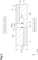
- FIG. 2 is a schematic cross-sectional view showing a first simulation condition.
- a model 30 in the first simulation includes a high thermal conduction portions 31, 32 and a low thermal conduction portion 33 similarly to the sheet member 3 of the above embodiment.
- the high thermal conduction portion 31 is exposed on one side in the thickness direction D1 and is located at one end of the model 30 in the alignment direction D2.
- the high thermal conduction portion 32 is exposed on the other side in the thickness direction D1 and is located at the other end of the model 30 in the alignment direction D2.
- the dimension of the high thermal conduction portions 31,32 along the thickness direction D1 was set to be the same.
- the low thermal conduction portion 33 had a sheet shape with a thickness of 1mm, and was integrated with the high thermal conduction portions 31, 32.
- the thermal conductivity of the high thermal conduction portions 31, 32 was set to 398W/mK, and the thermal conductivity of the low thermal conduction portion 33 was set to 0.3W/mK.
- the interval between the high thermal conduction portions 31, 32 along the alignment direction D2 is defined as an interval X (mm)
- the interval between the high thermal conduction portions 31, 32 along the thickness direction D1 is defined as an interval Y (mm) (interval Y is less than 1).
- the interval X is 0mm
- the edge 31a on the center side of the high thermal conduction portion 31 in the alignment direction D2 is overlapped with the edge 32a on the center side of the high thermal conduction portion 32 in the alignment direction D2 in the thickness direction D1.
- the edge 31b on the center side of the high thermal conduction portion 31 in the thickness direction D1 is overlapped with the edge 32b on the center side of the high thermal conduction portion 32 in the thickness direction D1 in the alignment direction D2.
- the temperature evaluation point 34 is located at the center of the interval Y on the edge 31a on the center side of the high thermal conduction portion 31 in the thickness direction D1. Therefore, when the interval Y is 0mm, the temperature evaluation point 34 is overlapped with the intersection of the edges 31a and 31b.
- the temperature evaluation point 35 is located at the center of the interval Y on the edge 32a on the center side of the high thermal conduction portion 32 in the thickness direction D1. Therefore, when the interval Y is 0mm, the temperature evaluation point 35 is overlapped with the intersection of the edges 32a and 32b.
- the one side of the model 30 is set as a side of the heat source, and the other side of the model 30 is set as a side of air.
- the temperature on the side of the heat source is set to 70°C
- the side of air is set to room temperature (23°C).
- the surface 30b of the model 30 located on the side of heat source in the thickness direction D1 is heated by natural convection and the surface 30a of the model 30 located on the side of air in the thickness direction D1 is cooled by natural convection.
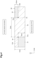
- FIG. 4 is a schematic cross-sectional view showing a second simulation condition.
- a model 50 in the simulation of second includes a high thermal conduction portions 51,52 and a low thermal conduction portion 53 similarly to the model 30.
- the positions where the high thermal conduction portions 51, 52 and the low thermal conduction portion 53 are provided in the model 50, and the thermal conductivities thereof are the same as those of the model 30.
- the interval between the high thermal conduction portions 51, 52 along the alignment direction D2 was set to 2mm.
- the length of the high thermal conduction portion 52 along the thickness direction D1 was set to Z mm, and the length of the high thermal conduction portion 51 along the thickness direction D1 was set to 1-Z mm.
- the ambient temperature condition of the model 50 is the same as that in the first simulation.
- the temperature evaluation point 54 is located at the intersection of the center side edge 51a of the high thermal conduction portion 51 along the alignment direction D2 and the center side edge 51b of the high thermal conduction portion 51 along the thickness direction D1.
- the temperature evaluation point 55 is located at the intersection of the center side edge 52a of the high thermal conduction portion 52 along the alignment direction D2 and the center side edge 52b of the high thermal conduction portion 52 along the thickness direction D1.
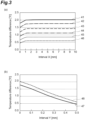
- FIG. 5 is a graph showing results of the second simulation, and shows a change in temperature difference of the temperature evaluation points 54, 55 when the height of the high thermal conduction portion 51 along the thickness direction D1 is changed.
- the horizontal axis represents the length Z
- the vertical axis represents the temperature difference at the temperature evaluation points 54, 55.
- the larger the length along the thickness direction D1 of the high thermal conduction portion 51 located on the side of heat source in the thickness direction D1 the larger the temperature difference. From this result, it is suggested that in order to widen the temperature difference of the temperature evaluation points 54, 55 along the alignment direction D2 in the model 50, it is effective to increase the thickness of the high thermal conductive portion located on the side of heat source as much as possible.
- FIG. 6 is a schematic cross-sectional view showing a third simulation condition.
- the model used in the third simulation has a structure in which it is estimated that the largest temperature difference occurs in the alignment direction D2.
- a model 60 in the third simulation includes a high thermal conduction portion 61 and a low thermal conduction portion 62.
- the high thermal conduction portion 61 and the low thermal conduction portion 62 are arranged in order along the alignment direction D2 and are integrated with each other.
- the dimensions of the high thermal conduction portion 61 and the low thermal conduction portion 62 along the thickness direction D1 are 1mm.
- the thermal conductivity of the high thermal conduction portion 61 is set to 398W/mK.
- the one side of the model 60 is set as the side of heat source, and the other side of the model 60 is set as the side of air.
- the temperature on the side of heat source is set to 100°C.
- the side of air has the same conditions as in the first simulation.
- a temperature evaluation point 63 located on surface 60a of the model 60 is set.
- the temperature evaluation point 63 is located on the low thermal conduction portion 62 at a distance of 2mm along the alignment direction D2 from the contact portion 64 between the high thermal conduction portion 61 and the low thermal conduction portion 62. Therefore, the temperature of temperature evaluation point 63 indicates the temperature of surface 60a when the model 60 is heated (more specifically, the temperature of surface 60a formed of the low thermal conduction portion 62).
- FIG. 7 is a graph showing results of the third simulation, and shows a temperature change of the temperature evaluation point 63 when the heat conductivity of the low thermal conduction portion 62 is changed.
- the horizontal axis represents the thermal conductivity of the low thermal conduction portion 62
- the vertical axis represents the temperature of the temperature evaluation point 63.
- the thermal conductivity of the low thermal conduction portion 62 was 0.2W/mK
- the temperature difference between the heat source and the temperature evaluation point 63 was about 8°C.
- the thermal conductivity of the low thermal conduction portion 62 was 0.08W/mK
- the temperature difference between the heat source and the temperature evaluation point 63 was about 15°C.
- the thermal conductivity of the low thermal conduction portion 62 was 30W/mK or more
- the temperature difference between the heat source and the temperature evaluation point 63 was almost 0. This suggests that, for example, when the thermal conductivity of the low thermal conduction portion 23 included in the sheet member 3 is 0.2W/mK or less, the low thermal conduction portion 23 is likely to exhibit good thermal insulation properties, and when the thermal conductivity of the low thermal conduction portion 23 is 0.08W/mK or less, the low thermal conduction portion 23 is likely to exhibit better thermal insulation properties.
- FIG. 8 is a schematic cross-sectional view of a thermoelectric conversion element according to a first reference example
- (b) of FIG. 8 is a schematic cross-sectional view of a thermoelectric conversion element according to a second reference example
- (c) of FIG. 8 is a schematic cross-sectional view of a thermoelectric conversion element according to a third reference example.
- the thermoelectric conversion element 101 shown in (a) of FIG. 8 includes a high thermal conduction portion 110 and a low thermal conduction portion 120 provided on the sealing layer 15 in addition to the components of the thermoelectric conversion element 1.
- the high thermal conduction portion 110 is provided to improve heat dissipation of the n-type thermoelectric conversion layer 14a and the p-type thermoelectric conversion layer 14b, and is overlapped with the contact portion CP in the thickness direction D1.
- the center of the high thermal conduction portion 110 in the alignment direction D2 is overlapped with the contact portion CP in the thickness direction D1.
- the low thermal conduction portion 120 is a sheet member provided to reduce heat dissipation of the first electrode 12, the second electrode 13, and their vicinity.
- the low thermal conduction portion 120 surrounds the high thermal conduction portion 110 in a direction orthogonal to the thickness direction D1 and is overlapped with the first electrode 12, the second electrode 13, the first high thermal conduction portion 21, and the second high thermal conduction portion 22 in the thickness direction D1. Lengths of the high thermal conduction portion 110 and the low thermal conduction portion 120 along the thickness direction D1 are the same.
- the thermoelectric conversion element 201 shown in (b) of FIG. 8 includes a low thermal conduction portion 220 provided on the sealing layer 15 in addition to the components of the thermoelectric conversion element 1.
- the low thermal conduction portion 220 is a sheet member covering the upper face of the sealing layer 15. Length of the low thermal conduction portion 220 along the thickness direction D1 is the same as the length of the high thermal conduction portion 110 and the low thermal conduction portion 120 along the thickness direction D1 shown in (a) of FIG. 8 .
- the thermoelectric conversion element 301 shown in (c) of FIG. 8 includes a high thermal conduction portion 310 provided on the sealing layer 15 in addition to the components of the thermoelectric conversion element 1.
- the high thermal conduction portion 310 is a sheet member covering the upper face of the sealing layer 15. Length of the high thermal conduction portion 310 along the thickness direction D1 is the same as the length of the high thermal conduction portion 110 and the low thermal conduction portion 120 along the thickness direction D1 shown in (a) of FIG. 8 .
- the length of the thermoelectric conversion module 2 along the thickness direction D1 was set to 0.6 mm
- the length of the substrate 11 along the thickness direction D1 was set to 50 ⁇ m
- the length of the sheet member 3 along the thickness direction D1 was set to 400 ⁇ m
- the lengths of the thermoelectric conversion module 2 and the sheet member 3 along the alignment direction D2 were set to 15mm.
- the length of the thermoelectric conversion module 2 along the thickness direction D1 does not include the lengths of the high thermal conduction portions 110, 310 along the thickness direction D1 and the lengths of the low thermal conduction portions 120, 220 along the thickness direction D1.
- the lengths of the first electrode 12 and the second electrode 13 along the thickness direction D1 were set to 25 ⁇ m, the lengths of the n-type thermoelectric conversion layer 14a and the p-type thermoelectric conversion layer 14b along the thickness direction D1 were set to 100 ⁇ m, the maximum length of the sealing layer 15 along the thickness direction D1 was set to 150 ⁇ m, the lengths of the first high thermal conduction portion 21, the second high thermal conduction portion 22 and the low thermal conduction portion 23 along the thickness direction D1 were set to 400 ⁇ m, the lengths of the first electrode 12 and the second electrode 13 along the alignment direction D2 were set to 3mm, the lengths of the n-type thermoelectric conversion layer 14a and the p-type thermoelectric conversion layer 14b were set to 2.5mm, and the lengths of the first high thermal conduction portion 21 and the second high thermal conduction portion 22 along the alignment direction D2 were set to 3mm.
- the length of the high thermal conduction portion 110 along the thickness direction D1 was set to 400 ⁇ m, and the length of the high thermal conduction
- thermoelectric conversion elements 1, 101, 201, 301 the thermal conductivities of the substrate 11 and the sealing layer 15 were set to 0.3W/mK, the thermal conductivities of the first electrode 12 and the second electrode 13 were set to 398W/mK, the thermal conductivities of the n-type thermoelectric conversion layer 14a and the p-type thermoelectric conversion layer 14b were set to 0.5W/mK, the thermal conductivities of the first high thermal conduction portion 21 and the second high thermal conduction portion 22 were set to 5.0W/mK, and the thermal conductivity of the low thermal conduction portion 23 was set to 0.05W/mK.
- the thermal conductivities of the high thermal conduction portions 110, 310 were set to 5.0W/mK, the thermal conductivity of the low thermal conduction portion 120 was set to 0.05W/mK, and the thermal conductivity of the low thermal conduction portion 220 was set to 0.1W/mK.
- thermoelectric conversion elements 1, 101, 201, 301 the temperature on a side of heat source is set to 100°C, and the temperature on a side of air is set to room temperature (23°C), similarly to the third simulation described above.
- the temperature of the exposed surface of the sheet member 3 crossing the thickness direction D1 was also set to 100°C.
- thermoelectric conversion elements 1, 101, 201, 301 set under the above-described conditions.
- the maximum temperature difference of the element portion 14 of the thermoelectric conversion element 1 was 5.259°C
- the maximum temperature difference of the element portion 14 of the thermoelectric conversion element 101 was 4.909°C
- the maximum temperature difference of the element portion 14 of the thermoelectric conversion element 201 was 4.785°C
- the maximum temperature difference of the element portion 14 of the thermoelectric conversion element 301 was 1.577°C.
- thermoelectric conversion element 101 When the maximum temperature difference of the element portion 14 of the thermoelectric conversion element 101 was taken as a reference (100%), the maximum temperature difference of the element portion 14 of the thermoelectric conversion element 1 was 107%, the maximum temperature difference of the element portion 14 of the thermoelectric conversion element 201 was 87%, and the maximum temperature difference of the element portion 14 of the thermoelectric conversion element 301 was 32%. From the above results, it was suggested that in the configuration including the thermoelectric conversion element 1, when the outermost layer located on the first main face 11a of the substrate 11 is formed of the sealing layer 15, the thermoelectric conversion efficiency is likely to be the highest.
- the outermost layer located on the first main face is formed only of the sealing layer, but the present disclosure is not limited thereto.
- the outermost layer may include the sealing layer and a member different from the sealing layer.
- thermoelectric conversion module is provided on the first main face.
- a plurality of thermoelectric conversion modules may be provided on the first main face.
- the plurality of thermoelectric conversion modules may be electrically connected to each other.
- the first electrode or the second electrode may be shared.
- the sheet member may include a high thermal conduction portion other than the first and the second high thermal conduction portions.
- first electrode and the second electrode are formed at the same time, however no limited thereto.
- the first and second electrodes may be formed from different materials.
Landscapes
- Cooling Or The Like Of Semiconductors Or Solid State Devices (AREA)
Claims (7)
- Thermoelektrisches Umwandlungselement (1, 101, 201, 301), das Folgendes umfasst:ein Substrat (11) mit einer ersten Hauptfläche (11a) und einer zweiten Hauptfläche (11b), die sich auf der gegenüberliegenden Seite der ersten Hauptfläche (11a) befindet;eine erste Elektrode (12), die auf der ersten Hauptfläche (11a) vorgesehen ist, eine thermoelektrische Umwandlungsschicht vom n-Typ (14a), die elektrisch mit der ersten Elektrode (12) verbunden ist, eine thermoelektrische Umwandlungsschicht vom p-Typ (14b), die in Kontakt mit der thermoelektrischen Umwandlungsschicht vom n-Typ (14a) steht, und eine zweite Elektrode (13), die elektrisch mit der thermoelektrischen Umwandlungsschicht vom p-Typ (14b) verbunden ist;eine Dichtungsschicht (15), die auf der ersten Hauptfläche (11a) vorgesehen ist, wobei die Dichtungsschicht (15) die erste Elektrode (12), die thermoelektrische Umwandlungsschicht vom n-Typ (14a), die thermoelektrische Umwandlungsschicht vom p-Typ (14b) und die zweite Elektrode (13) bedeckt; undeinen ersten hoch wärmeleitenden Abschnitt (21), einen zweiten hoch wärmeleitenden Abschnitt (22) und einen niedrig wärmeleitenden Abschnitt (23), die nur auf der zweiten Hauptfläche (11b) vorgesehen sind,wobei die erste Elektrode (12), die thermoelektrische Umwandlungsschicht vom n-Typ (14a), die thermoelektrische Umwandlungsschicht vom p-Typ (14b) und die zweite Elektrode (13) in der Reihenfolge entlang einer Ausrichtungsrichtung orthogonal zu einer Dickenrichtung des Substrats (11) angeordnet sind,wobei die erste Elektrode (12) mit dem ersten hoch wärmeleitenden Abschnitt (21) in der Dickenrichtung überlappt ist, die zweite Elektrode (13) mit dem zweiten hoch wärmeleitenden Abschnitt (22) in der Dickenrichtung überlappt ist und ein Kontaktabschnitt (CP) zwischen der thermoelektrischen Umwandlungsschicht vom n-Typ (14a) und der thermoelektrischen Umwandlungsschicht vom p-Typ (14b) mit dem niedrig wärmeleitenden Abschnitt (23) in der Dickenrichtung überlappt ist, undwobei die Dichtungsschicht (15) eine äußerste Schicht bildet, die sich auf der ersten Hauptfläche (11a) befindet.
- Thermoelektrisches Umwandlungselement (1, 101, 201, 301) nach Anspruch 1, wobei die Wärmeleitfähigkeit des niedrig wärmeleitenden Abschnitts (23) 0,2 W/mK oder weniger beträgt.
- Thermoelektrisches Umwandlungselement (1, 101, 201, 301) nach Anspruch 1 oder 2, wobei die Wärmeleitfähigkeit des niedrig wärmeleitenden Abschnitts (23) 0,08 W/mK oder weniger beträgt.
- Thermoelektrisches Umwandlungselement (1, 101, 201, 301) nach einem der Ansprüche 1 bis 3, wobei die Wärmeleitfähigkeit des ersten hoch wärmeleitenden Abschnitts (21) und die Wärmeleitfähigkeit des zweiten hoch wärmeleitenden Abschnitts (22) 5 W/mK oder mehr betragen.
- Thermoelektrisches Umwandlungselement (1, 101, 201, 301) nach einem der Ansprüche 1 bis 4, wobei die Wärmeleitfähigkeit der ersten Elektrode (12) und die Wärmeleitfähigkeit der zweiten Elektrode (13) 5 W/mK oder mehr betragen.
- Thermoelektrisches Umwandlungselement (1, 101, 201, 301) nach einem der Ansprüche 1 bis 5, wobei das Substrat (11) eine Flexibilität aufweist.
- Thermoelektrisches Umwandlungselement (1, 101, 201, 301) nach einem der Ansprüche 1 bis 6,wobei ein Abstand von dem ersten hoch wärmeleitenden Abschnitt (21) zu dem Kontaktabschnitt (CP) entlang der Ausrichtungsrichtung 5 mal oder mehr länger ist als eine Länge des ersten hoch wärmeleitenden Abschnitts (21) entlang der Dickenrichtung; undwobei ein Abstand von dem zweiten hoch wärmeleitenden Abschnitt (22) zu dem Kontaktabschnitt (CP) entlang der Ausrichtungsrichtung 5 mal oder mehr länger ist als eine Länge des zweiten hoch wärmeleitenden Abschnitts (22) entlang der Dickenrichtung.
Applications Claiming Priority (2)
| Application Number | Priority Date | Filing Date | Title |
|---|---|---|---|
| JP2019146664 | 2019-08-08 | ||
| PCT/JP2020/029999 WO2021025060A1 (ja) | 2019-08-08 | 2020-08-05 | 熱電変換素子 |
Publications (3)
| Publication Number | Publication Date |
|---|---|
| EP4012787A1 EP4012787A1 (de) | 2022-06-15 |
| EP4012787A4 EP4012787A4 (de) | 2022-10-05 |
| EP4012787B1 true EP4012787B1 (de) | 2024-01-03 |
Family
ID=74502718
Family Applications (1)
| Application Number | Title | Priority Date | Filing Date |
|---|---|---|---|
| EP20849156.3A Active EP4012787B1 (de) | 2019-08-08 | 2020-08-05 | Thermoelektrisches umwandlungselement |
Country Status (5)
| Country | Link |
|---|---|
| US (2) | US20220293843A1 (de) |
| EP (1) | EP4012787B1 (de) |
| JP (1) | JP7662522B2 (de) |
| CN (1) | CN114207851A (de) |
| WO (1) | WO2021025060A1 (de) |
Families Citing this family (3)
| Publication number | Priority date | Publication date | Assignee | Title |
|---|---|---|---|---|
| JP7829674B2 (ja) * | 2022-03-08 | 2026-03-13 | デンカ株式会社 | 熱電変換モジュール及びその製造方法 |
| CN119422472A (zh) * | 2022-06-24 | 2025-02-11 | 电化株式会社 | 热电转换模块及其制造方法 |
| JP7756674B2 (ja) * | 2023-03-31 | 2025-10-20 | リンテック株式会社 | 熱電変換モジュール |
Family Cites Families (19)
| Publication number | Priority date | Publication date | Assignee | Title |
|---|---|---|---|---|
| JP3981738B2 (ja) * | 2004-12-28 | 2007-09-26 | 国立大学法人長岡技術科学大学 | 熱電変換素子 |
| JP4895293B2 (ja) | 2007-01-26 | 2012-03-14 | 新日鐵化学株式会社 | フレキシブル熱電変換素子及びその製造方法 |
| JP5087757B2 (ja) * | 2007-06-08 | 2012-12-05 | 住友金属鉱山株式会社 | 熱電変換モジュールとこれを用いた発電装置 |
| JP5298532B2 (ja) * | 2007-12-27 | 2013-09-25 | ダイキン工業株式会社 | 熱電素子 |
| JP5067352B2 (ja) * | 2008-12-05 | 2012-11-07 | 住友金属鉱山株式会社 | 熱電変換モジュールとこれを用いた発電装置 |
| CN102263197B (zh) * | 2011-07-22 | 2013-02-27 | 江苏物联网研究发展中心 | 新型微型热电发生器及其制造方法 |
| WO2013121486A1 (ja) * | 2012-02-16 | 2013-08-22 | 日本電気株式会社 | 熱電変換モジュール装置、及び電子機器 |
| US9780283B2 (en) * | 2013-03-21 | 2017-10-03 | National University Corporation Nagaoka University Of Technology | Thermoelectric conversion element |
| JP6519085B2 (ja) * | 2013-09-25 | 2019-05-29 | リンテック株式会社 | 熱伝導性接着シート、その製造方法及びそれを用いた電子デバイス |
| US9944831B2 (en) * | 2013-09-25 | 2018-04-17 | Lintec Corporation | Heat-conductive adhesive sheet, manufacturing method for same, and electronic device using same |
| JP6539917B2 (ja) * | 2014-12-26 | 2019-07-10 | リンテック株式会社 | 熱伝導性接着シート、その製造方法及びそれを用いた電子デバイス |
| CN105099275B (zh) * | 2015-07-29 | 2017-08-25 | 浙江大学 | 具有微凸台阵列热端的平面型温差发电结构 |
| JP6672562B2 (ja) * | 2015-08-20 | 2020-03-25 | リンテック株式会社 | ペルチェ冷却素子及びその製造方法 |
| WO2017051699A1 (ja) * | 2015-09-24 | 2017-03-30 | 富士フイルム株式会社 | 熱電変換素子 |
| WO2018061462A1 (ja) * | 2016-09-28 | 2018-04-05 | Tdk株式会社 | 熱電変換装置 |
| WO2018139475A1 (ja) * | 2017-01-27 | 2018-08-02 | リンテック株式会社 | フレキシブル熱電変換素子及びその製造方法 |
| JP7183794B2 (ja) * | 2017-01-31 | 2022-12-06 | 日本ゼオン株式会社 | 熱電変換モジュール |
| WO2018143185A1 (ja) * | 2017-01-31 | 2018-08-09 | 日本ゼオン株式会社 | 熱電変換モジュール |
| WO2018179546A1 (ja) * | 2017-03-30 | 2018-10-04 | リンテック株式会社 | 熱電変換モジュール |
-
2020
- 2020-08-05 EP EP20849156.3A patent/EP4012787B1/de active Active
- 2020-08-05 WO PCT/JP2020/029999 patent/WO2021025060A1/ja not_active Ceased
- 2020-08-05 CN CN202080056159.9A patent/CN114207851A/zh active Pending
- 2020-08-05 JP JP2021537345A patent/JP7662522B2/ja active Active
- 2020-08-05 US US17/633,087 patent/US20220293843A1/en not_active Abandoned
-
2024
- 2024-09-05 US US18/825,858 patent/US20240431207A1/en active Pending
Also Published As
| Publication number | Publication date |
|---|---|
| JP7662522B2 (ja) | 2025-04-15 |
| US20220293843A1 (en) | 2022-09-15 |
| EP4012787A1 (de) | 2022-06-15 |
| WO2021025060A1 (ja) | 2021-02-11 |
| JPWO2021025060A1 (de) | 2021-02-11 |
| EP4012787A4 (de) | 2022-10-05 |
| CN114207851A (zh) | 2022-03-18 |
| US20240431207A1 (en) | 2024-12-26 |
Similar Documents
| Publication | Publication Date | Title |
|---|---|---|
| US20240431207A1 (en) | Composite, layer including the composite, and module including the layer | |
| US11075331B2 (en) | Thermoelectric device having circuitry with structural rigidity | |
| US8148812B2 (en) | Thermal resistor, semiconductor device using the same, and electric device | |
| KR102182765B1 (ko) | 열전 변환 소자 | |
| EP2023388B1 (de) | Halbleiterpaket | |
| WO2013114854A1 (ja) | 有機熱電発電素子およびその製造方法 | |
| JP5857792B2 (ja) | 熱電デバイスおよびその製造方法 | |
| WO2013121486A1 (ja) | 熱電変換モジュール装置、及び電子機器 | |
| CN101911323A (zh) | 热电元件 | |
| US20180175272A1 (en) | Thermoelectric conversion module | |
| JP2016187008A (ja) | 熱電変換デバイス | |
| KR20130033865A (ko) | 열전모듈 및 열전모듈 제조방법 | |
| EP4012788B1 (de) | Thermoelektrisches umwandlungselement | |
| WO2018143178A1 (ja) | 熱電変換モジュール | |
| US10347811B2 (en) | Thermoelectric conversion module | |
| US10236431B2 (en) | Thermoelectric conversion element and thermoelectric conversion module | |
| US20180026172A1 (en) | Thermoelectric conversion element and thermoelectric conversion module | |
| US11430936B2 (en) | Thermoelectric module | |
| EP4577027A1 (de) | Thermoelektrisches wandlermodul | |
| JP6505585B2 (ja) | 熱電変換素子 | |
| JP2024146616A (ja) | 熱電変換モジュール |
Legal Events
| Date | Code | Title | Description |
|---|---|---|---|
| STAA | Information on the status of an ep patent application or granted ep patent |
Free format text: STATUS: THE INTERNATIONAL PUBLICATION HAS BEEN MADE |
|
| PUAI | Public reference made under article 153(3) epc to a published international application that has entered the european phase |
Free format text: ORIGINAL CODE: 0009012 |
|
| STAA | Information on the status of an ep patent application or granted ep patent |
Free format text: STATUS: REQUEST FOR EXAMINATION WAS MADE |
|
| 17P | Request for examination filed |
Effective date: 20220301 |
|
| AK | Designated contracting states |
Kind code of ref document: A1 Designated state(s): AL AT BE BG CH CY CZ DE DK EE ES FI FR GB GR HR HU IE IS IT LI LT LU LV MC MK MT NL NO PL PT RO RS SE SI SK SM TR |
|
| A4 | Supplementary search report drawn up and despatched |
Effective date: 20220905 |
|
| RIC1 | Information provided on ipc code assigned before grant |
Ipc: H02N 11/00 20060101ALI20220830BHEP Ipc: H01L 35/30 20060101AFI20220830BHEP |
|
| DAV | Request for validation of the european patent (deleted) | ||
| DAX | Request for extension of the european patent (deleted) | ||
| REG | Reference to a national code |
Ref legal event code: R079 Ref country code: DE Ref legal event code: R079 Ref document number: 602020024023 Country of ref document: DE Free format text: PREVIOUS MAIN CLASS: H01L0035300000 Ipc: H10N0010130000 |
|
| RIC1 | Information provided on ipc code assigned before grant |
Ipc: H02N 11/00 20060101ALI20230606BHEP Ipc: H10N 10/13 20230101AFI20230606BHEP |
|
| GRAP | Despatch of communication of intention to grant a patent |
Free format text: ORIGINAL CODE: EPIDOSNIGR1 |
|
| STAA | Information on the status of an ep patent application or granted ep patent |
Free format text: STATUS: GRANT OF PATENT IS INTENDED |
|
| INTG | Intention to grant announced |
Effective date: 20230824 |
|
| RIN1 | Information on inventor provided before grant (corrected) |
Inventor name: GOTO, YOSHITSUGU Inventor name: ASAMI, TAKESHI |
|
| GRAS | Grant fee paid |
Free format text: ORIGINAL CODE: EPIDOSNIGR3 |
|
| GRAA | (expected) grant |
Free format text: ORIGINAL CODE: 0009210 |
|
| STAA | Information on the status of an ep patent application or granted ep patent |
Free format text: STATUS: THE PATENT HAS BEEN GRANTED |
|
| AK | Designated contracting states |
Kind code of ref document: B1 Designated state(s): AL AT BE BG CH CY CZ DE DK EE ES FI FR GB GR HR HU IE IS IT LI LT LU LV MC MK MT NL NO PL PT RO RS SE SI SK SM TR |
|
| REG | Reference to a national code |
Ref country code: GB Ref legal event code: FG4D |
|
| REG | Reference to a national code |
Ref country code: CH Ref legal event code: EP |
|
| REG | Reference to a national code |
Ref country code: DE Ref legal event code: R096 Ref document number: 602020024023 Country of ref document: DE |
|
| REG | Reference to a national code |
Ref country code: IE Ref legal event code: FG4D |
|
| P01 | Opt-out of the competence of the unified patent court (upc) registered |
Effective date: 20231228 |
|
| REG | Reference to a national code |
Ref country code: LT Ref legal event code: MG9D |
|
| PG25 | Lapsed in a contracting state [announced via postgrant information from national office to epo] |
Ref country code: ES Free format text: LAPSE BECAUSE OF FAILURE TO SUBMIT A TRANSLATION OF THE DESCRIPTION OR TO PAY THE FEE WITHIN THE PRESCRIBED TIME-LIMIT Effective date: 20240103 |
|
| PG25 | Lapsed in a contracting state [announced via postgrant information from national office to epo] |
Ref country code: ES Free format text: LAPSE BECAUSE OF FAILURE TO SUBMIT A TRANSLATION OF THE DESCRIPTION OR TO PAY THE FEE WITHIN THE PRESCRIBED TIME-LIMIT Effective date: 20240103 |
|
| REG | Reference to a national code |
Ref country code: NL Ref legal event code: MP Effective date: 20240103 |
|
| REG | Reference to a national code |
Ref country code: AT Ref legal event code: MK05 Ref document number: 1648095 Country of ref document: AT Kind code of ref document: T Effective date: 20240103 |
|
| PG25 | Lapsed in a contracting state [announced via postgrant information from national office to epo] |
Ref country code: NL Free format text: LAPSE BECAUSE OF FAILURE TO SUBMIT A TRANSLATION OF THE DESCRIPTION OR TO PAY THE FEE WITHIN THE PRESCRIBED TIME-LIMIT Effective date: 20240103 |
|
| PG25 | Lapsed in a contracting state [announced via postgrant information from national office to epo] |
Ref country code: NL Free format text: LAPSE BECAUSE OF FAILURE TO SUBMIT A TRANSLATION OF THE DESCRIPTION OR TO PAY THE FEE WITHIN THE PRESCRIBED TIME-LIMIT Effective date: 20240103 |
|
| PG25 | Lapsed in a contracting state [announced via postgrant information from national office to epo] |
Ref country code: IS Free format text: LAPSE BECAUSE OF FAILURE TO SUBMIT A TRANSLATION OF THE DESCRIPTION OR TO PAY THE FEE WITHIN THE PRESCRIBED TIME-LIMIT Effective date: 20240503 |
|
| PG25 | Lapsed in a contracting state [announced via postgrant information from national office to epo] |
Ref country code: LT Free format text: LAPSE BECAUSE OF FAILURE TO SUBMIT A TRANSLATION OF THE DESCRIPTION OR TO PAY THE FEE WITHIN THE PRESCRIBED TIME-LIMIT Effective date: 20240103 |
|
| PG25 | Lapsed in a contracting state [announced via postgrant information from national office to epo] |
Ref country code: GR Free format text: LAPSE BECAUSE OF FAILURE TO SUBMIT A TRANSLATION OF THE DESCRIPTION OR TO PAY THE FEE WITHIN THE PRESCRIBED TIME-LIMIT Effective date: 20240404 |
|
| PG25 | Lapsed in a contracting state [announced via postgrant information from national office to epo] |
Ref country code: RS Free format text: LAPSE BECAUSE OF FAILURE TO SUBMIT A TRANSLATION OF THE DESCRIPTION OR TO PAY THE FEE WITHIN THE PRESCRIBED TIME-LIMIT Effective date: 20240403 Ref country code: HR Free format text: LAPSE BECAUSE OF FAILURE TO SUBMIT A TRANSLATION OF THE DESCRIPTION OR TO PAY THE FEE WITHIN THE PRESCRIBED TIME-LIMIT Effective date: 20240103 |
|
| PG25 | Lapsed in a contracting state [announced via postgrant information from national office to epo] |
Ref country code: AT Free format text: LAPSE BECAUSE OF FAILURE TO SUBMIT A TRANSLATION OF THE DESCRIPTION OR TO PAY THE FEE WITHIN THE PRESCRIBED TIME-LIMIT Effective date: 20240103 Ref country code: CZ Free format text: LAPSE BECAUSE OF FAILURE TO SUBMIT A TRANSLATION OF THE DESCRIPTION OR TO PAY THE FEE WITHIN THE PRESCRIBED TIME-LIMIT Effective date: 20240103 |
|
| PG25 | Lapsed in a contracting state [announced via postgrant information from national office to epo] |
Ref country code: RS Free format text: LAPSE BECAUSE OF FAILURE TO SUBMIT A TRANSLATION OF THE DESCRIPTION OR TO PAY THE FEE WITHIN THE PRESCRIBED TIME-LIMIT Effective date: 20240403 Ref country code: NO Free format text: LAPSE BECAUSE OF FAILURE TO SUBMIT A TRANSLATION OF THE DESCRIPTION OR TO PAY THE FEE WITHIN THE PRESCRIBED TIME-LIMIT Effective date: 20240403 Ref country code: LT Free format text: LAPSE BECAUSE OF FAILURE TO SUBMIT A TRANSLATION OF THE DESCRIPTION OR TO PAY THE FEE WITHIN THE PRESCRIBED TIME-LIMIT Effective date: 20240103 Ref country code: IS Free format text: LAPSE BECAUSE OF FAILURE TO SUBMIT A TRANSLATION OF THE DESCRIPTION OR TO PAY THE FEE WITHIN THE PRESCRIBED TIME-LIMIT Effective date: 20240503 Ref country code: HR Free format text: LAPSE BECAUSE OF FAILURE TO SUBMIT A TRANSLATION OF THE DESCRIPTION OR TO PAY THE FEE WITHIN THE PRESCRIBED TIME-LIMIT Effective date: 20240103 Ref country code: GR Free format text: LAPSE BECAUSE OF FAILURE TO SUBMIT A TRANSLATION OF THE DESCRIPTION OR TO PAY THE FEE WITHIN THE PRESCRIBED TIME-LIMIT Effective date: 20240404 Ref country code: CZ Free format text: LAPSE BECAUSE OF FAILURE TO SUBMIT A TRANSLATION OF THE DESCRIPTION OR TO PAY THE FEE WITHIN THE PRESCRIBED TIME-LIMIT Effective date: 20240103 Ref country code: BG Free format text: LAPSE BECAUSE OF FAILURE TO SUBMIT A TRANSLATION OF THE DESCRIPTION OR TO PAY THE FEE WITHIN THE PRESCRIBED TIME-LIMIT Effective date: 20240103 Ref country code: AT Free format text: LAPSE BECAUSE OF FAILURE TO SUBMIT A TRANSLATION OF THE DESCRIPTION OR TO PAY THE FEE WITHIN THE PRESCRIBED TIME-LIMIT Effective date: 20240103 |
|
| PG25 | Lapsed in a contracting state [announced via postgrant information from national office to epo] |
Ref country code: PL Free format text: LAPSE BECAUSE OF FAILURE TO SUBMIT A TRANSLATION OF THE DESCRIPTION OR TO PAY THE FEE WITHIN THE PRESCRIBED TIME-LIMIT Effective date: 20240103 Ref country code: PT Free format text: LAPSE BECAUSE OF FAILURE TO SUBMIT A TRANSLATION OF THE DESCRIPTION OR TO PAY THE FEE WITHIN THE PRESCRIBED TIME-LIMIT Effective date: 20240503 |
|
| PG25 | Lapsed in a contracting state [announced via postgrant information from national office to epo] |
Ref country code: SE Free format text: LAPSE BECAUSE OF FAILURE TO SUBMIT A TRANSLATION OF THE DESCRIPTION OR TO PAY THE FEE WITHIN THE PRESCRIBED TIME-LIMIT Effective date: 20240103 Ref country code: PT Free format text: LAPSE BECAUSE OF FAILURE TO SUBMIT A TRANSLATION OF THE DESCRIPTION OR TO PAY THE FEE WITHIN THE PRESCRIBED TIME-LIMIT Effective date: 20240503 Ref country code: PL Free format text: LAPSE BECAUSE OF FAILURE TO SUBMIT A TRANSLATION OF THE DESCRIPTION OR TO PAY THE FEE WITHIN THE PRESCRIBED TIME-LIMIT Effective date: 20240103 Ref country code: LV Free format text: LAPSE BECAUSE OF FAILURE TO SUBMIT A TRANSLATION OF THE DESCRIPTION OR TO PAY THE FEE WITHIN THE PRESCRIBED TIME-LIMIT Effective date: 20240103 |
|
| REG | Reference to a national code |
Ref country code: DE Ref legal event code: R097 Ref document number: 602020024023 Country of ref document: DE |
|
| PG25 | Lapsed in a contracting state [announced via postgrant information from national office to epo] |
Ref country code: DK Free format text: LAPSE BECAUSE OF FAILURE TO SUBMIT A TRANSLATION OF THE DESCRIPTION OR TO PAY THE FEE WITHIN THE PRESCRIBED TIME-LIMIT Effective date: 20240103 |
|
| PG25 | Lapsed in a contracting state [announced via postgrant information from national office to epo] |
Ref country code: SM Free format text: LAPSE BECAUSE OF FAILURE TO SUBMIT A TRANSLATION OF THE DESCRIPTION OR TO PAY THE FEE WITHIN THE PRESCRIBED TIME-LIMIT Effective date: 20240103 |
|
| PG25 | Lapsed in a contracting state [announced via postgrant information from national office to epo] |
Ref country code: EE Free format text: LAPSE BECAUSE OF FAILURE TO SUBMIT A TRANSLATION OF THE DESCRIPTION OR TO PAY THE FEE WITHIN THE PRESCRIBED TIME-LIMIT Effective date: 20240103 |
|
| PG25 | Lapsed in a contracting state [announced via postgrant information from national office to epo] |
Ref country code: SK Free format text: LAPSE BECAUSE OF FAILURE TO SUBMIT A TRANSLATION OF THE DESCRIPTION OR TO PAY THE FEE WITHIN THE PRESCRIBED TIME-LIMIT Effective date: 20240103 |
|
| PG25 | Lapsed in a contracting state [announced via postgrant information from national office to epo] |
Ref country code: SM Free format text: LAPSE BECAUSE OF FAILURE TO SUBMIT A TRANSLATION OF THE DESCRIPTION OR TO PAY THE FEE WITHIN THE PRESCRIBED TIME-LIMIT Effective date: 20240103 Ref country code: SK Free format text: LAPSE BECAUSE OF FAILURE TO SUBMIT A TRANSLATION OF THE DESCRIPTION OR TO PAY THE FEE WITHIN THE PRESCRIBED TIME-LIMIT Effective date: 20240103 Ref country code: RO Free format text: LAPSE BECAUSE OF FAILURE TO SUBMIT A TRANSLATION OF THE DESCRIPTION OR TO PAY THE FEE WITHIN THE PRESCRIBED TIME-LIMIT Effective date: 20240103 Ref country code: EE Free format text: LAPSE BECAUSE OF FAILURE TO SUBMIT A TRANSLATION OF THE DESCRIPTION OR TO PAY THE FEE WITHIN THE PRESCRIBED TIME-LIMIT Effective date: 20240103 Ref country code: DK Free format text: LAPSE BECAUSE OF FAILURE TO SUBMIT A TRANSLATION OF THE DESCRIPTION OR TO PAY THE FEE WITHIN THE PRESCRIBED TIME-LIMIT Effective date: 20240103 |
|
| PLBE | No opposition filed within time limit |
Free format text: ORIGINAL CODE: 0009261 |
|
| STAA | Information on the status of an ep patent application or granted ep patent |
Free format text: STATUS: NO OPPOSITION FILED WITHIN TIME LIMIT |
|
| 26N | No opposition filed |
Effective date: 20241007 |
|
| REG | Reference to a national code |
Ref country code: CH Ref legal event code: PL |
|
| PG25 | Lapsed in a contracting state [announced via postgrant information from national office to epo] |
Ref country code: LU Free format text: LAPSE BECAUSE OF NON-PAYMENT OF DUE FEES Effective date: 20240805 |
|
| PG25 | Lapsed in a contracting state [announced via postgrant information from national office to epo] |
Ref country code: CH Free format text: LAPSE BECAUSE OF NON-PAYMENT OF DUE FEES Effective date: 20240831 Ref country code: SI Free format text: LAPSE BECAUSE OF FAILURE TO SUBMIT A TRANSLATION OF THE DESCRIPTION OR TO PAY THE FEE WITHIN THE PRESCRIBED TIME-LIMIT Effective date: 20240103 Ref country code: MC Free format text: LAPSE BECAUSE OF FAILURE TO SUBMIT A TRANSLATION OF THE DESCRIPTION OR TO PAY THE FEE WITHIN THE PRESCRIBED TIME-LIMIT Effective date: 20240103 |
|
| REG | Reference to a national code |
Ref country code: BE Ref legal event code: MM Effective date: 20240831 |
|
| PG25 | Lapsed in a contracting state [announced via postgrant information from national office to epo] |
Ref country code: BE Free format text: LAPSE BECAUSE OF NON-PAYMENT OF DUE FEES Effective date: 20240831 |
|
| PG25 | Lapsed in a contracting state [announced via postgrant information from national office to epo] |
Ref country code: IE Free format text: LAPSE BECAUSE OF NON-PAYMENT OF DUE FEES Effective date: 20240805 |
|
| PG25 | Lapsed in a contracting state [announced via postgrant information from national office to epo] |
Ref country code: FI Free format text: LAPSE BECAUSE OF FAILURE TO SUBMIT A TRANSLATION OF THE DESCRIPTION OR TO PAY THE FEE WITHIN THE PRESCRIBED TIME-LIMIT Effective date: 20240103 |
|
| PGFP | Annual fee paid to national office [announced via postgrant information from national office to epo] |
Ref country code: DE Payment date: 20250702 Year of fee payment: 6 |
|
| PGFP | Annual fee paid to national office [announced via postgrant information from national office to epo] |
Ref country code: IT Payment date: 20250722 Year of fee payment: 6 |
|
| PGFP | Annual fee paid to national office [announced via postgrant information from national office to epo] |
Ref country code: GB Payment date: 20250703 Year of fee payment: 6 |
|
| PGFP | Annual fee paid to national office [announced via postgrant information from national office to epo] |
Ref country code: FR Payment date: 20250703 Year of fee payment: 6 |
|
| PG25 | Lapsed in a contracting state [announced via postgrant information from national office to epo] |
Ref country code: CY Free format text: LAPSE BECAUSE OF FAILURE TO SUBMIT A TRANSLATION OF THE DESCRIPTION OR TO PAY THE FEE WITHIN THE PRESCRIBED TIME-LIMIT; INVALID AB INITIO Effective date: 20200805 |
|
| PG25 | Lapsed in a contracting state [announced via postgrant information from national office to epo] |
Ref country code: HU Free format text: LAPSE BECAUSE OF FAILURE TO SUBMIT A TRANSLATION OF THE DESCRIPTION OR TO PAY THE FEE WITHIN THE PRESCRIBED TIME-LIMIT; INVALID AB INITIO Effective date: 20200805 |