EP4006560B1 - Diagnoseschaltung für parallel-struktur-mosfets mit mux und diagnoseverfahren damit - Google Patents
Diagnoseschaltung für parallel-struktur-mosfets mit mux und diagnoseverfahren damit Download PDFInfo
- Publication number
- EP4006560B1 EP4006560B1 EP20889077.2A EP20889077A EP4006560B1 EP 4006560 B1 EP4006560 B1 EP 4006560B1 EP 20889077 A EP20889077 A EP 20889077A EP 4006560 B1 EP4006560 B1 EP 4006560B1
- Authority
- EP
- European Patent Office
- Prior art keywords
- mosfets
- mosfet
- battery pack
- vehicle
- voltage
- Prior art date
- Legal status (The legal status is an assumption and is not a legal conclusion. Google has not performed a legal analysis and makes no representation as to the accuracy of the status listed.)
- Active
Links
Images


Classifications
-
- G—PHYSICS
- G01—MEASURING; TESTING
- G01R—MEASURING ELECTRIC VARIABLES; MEASURING MAGNETIC VARIABLES
- G01R31/00—Arrangements for testing electric properties; Arrangements for locating electric faults; Arrangements for electrical testing characterised by what is being tested not provided for elsewhere
-
- B—PERFORMING OPERATIONS; TRANSPORTING
- B60—VEHICLES IN GENERAL
- B60W—CONJOINT CONTROL OF VEHICLE SUB-UNITS OF DIFFERENT TYPE OR DIFFERENT FUNCTION; CONTROL SYSTEMS SPECIALLY ADAPTED FOR HYBRID VEHICLES; ROAD VEHICLE DRIVE CONTROL SYSTEMS FOR PURPOSES NOT RELATED TO THE CONTROL OF A PARTICULAR SUB-UNIT
- B60W50/00—Details of control systems for road vehicle drive control not related to the control of a particular sub-unit, e.g. process diagnostic or vehicle driver interfaces
- B60W50/02—Ensuring safety in case of control system failures, e.g. by diagnosing, circumventing or fixing failures
- B60W50/0205—Diagnosing or detecting failures; Failure detection models
-
- G—PHYSICS
- G01—MEASURING; TESTING
- G01R—MEASURING ELECTRIC VARIABLES; MEASURING MAGNETIC VARIABLES
- G01R31/00—Arrangements for testing electric properties; Arrangements for locating electric faults; Arrangements for electrical testing characterised by what is being tested not provided for elsewhere
- G01R31/26—Testing of individual semiconductor devices
- G01R31/2607—Circuits therefor
- G01R31/2621—Circuits therefor for testing field effect transistors, i.e. FET's
-
- G—PHYSICS
- G01—MEASURING; TESTING
- G01R—MEASURING ELECTRIC VARIABLES; MEASURING MAGNETIC VARIABLES
- G01R31/00—Arrangements for testing electric properties; Arrangements for locating electric faults; Arrangements for electrical testing characterised by what is being tested not provided for elsewhere
- G01R31/26—Testing of individual semiconductor devices
- G01R31/27—Testing of devices without physical removal from the circuit of which they form part, e.g. compensating for effects surrounding elements
-
- G—PHYSICS
- G01—MEASURING; TESTING
- G01R—MEASURING ELECTRIC VARIABLES; MEASURING MAGNETIC VARIABLES
- G01R31/00—Arrangements for testing electric properties; Arrangements for locating electric faults; Arrangements for electrical testing characterised by what is being tested not provided for elsewhere
- G01R31/327—Testing of circuit interrupters, switches or circuit-breakers
- G01R31/3277—Testing of circuit interrupters, switches or circuit-breakers of low voltage devices, e.g. domestic or industrial devices, such as motor protections, relays, rotation switches
-
- H—ELECTRICITY
- H01—ELECTRIC ELEMENTS
- H01M—PROCESSES OR MEANS, e.g. BATTERIES, FOR THE DIRECT CONVERSION OF CHEMICAL ENERGY INTO ELECTRICAL ENERGY
- H01M10/00—Secondary cells; Manufacture thereof
- H01M10/42—Methods or arrangements for servicing or maintenance of secondary cells or secondary half-cells
-
- H—ELECTRICITY
- H01—ELECTRIC ELEMENTS
- H01M—PROCESSES OR MEANS, e.g. BATTERIES, FOR THE DIRECT CONVERSION OF CHEMICAL ENERGY INTO ELECTRICAL ENERGY
- H01M10/00—Secondary cells; Manufacture thereof
- H01M10/42—Methods or arrangements for servicing or maintenance of secondary cells or secondary half-cells
- H01M10/425—Structural combination with electronic components, e.g. electronic circuits integrated to the outside of the casing
-
- H—ELECTRICITY
- H01—ELECTRIC ELEMENTS
- H01M—PROCESSES OR MEANS, e.g. BATTERIES, FOR THE DIRECT CONVERSION OF CHEMICAL ENERGY INTO ELECTRICAL ENERGY
- H01M10/00—Secondary cells; Manufacture thereof
- H01M10/42—Methods or arrangements for servicing or maintenance of secondary cells or secondary half-cells
- H01M10/4285—Testing apparatus
-
- H—ELECTRICITY
- H01—ELECTRIC ELEMENTS
- H01M—PROCESSES OR MEANS, e.g. BATTERIES, FOR THE DIRECT CONVERSION OF CHEMICAL ENERGY INTO ELECTRICAL ENERGY
- H01M2220/00—Batteries for particular applications
- H01M2220/20—Batteries in motive systems, e.g. vehicle, ship, plane
Definitions
- the present invention relates to a diagnosis circuit of parallel-structure MOSFETs including a MUX and a diagnosis method using the same. More particularly, the present invention relates to a circuit capable of diagnosing failure of a specific MOSFET, among a plurality of MOSFETs configured to supply power to a vehicle, the MOSFETs being connected to each other in parallel, using a MUX and a method of diagnosing failure of a specific MOSFET, among a plurality of MOSFETs connected to each other in parallel, using the same.
- a secondary battery applicable to an electric vehicle is generally used in a configuration in which a plurality of secondary battery cells is assembled.
- a secondary battery pack having a multi-module structure in which a plurality of secondary battery cells is connected to each other in series/parallel is generally used.
- a secondary battery pack is provided as an apparatus separate from an electric vehicle.
- a relay for electrical ON/OFF connection is provided between the secondary battery pack and the electric vehicle.
- 12 V, 48 V, or 400 V are generally used as voltages supplied by a secondary battery pack for vehicles.
- 400 V a mechanical relay is used due to physical limitation.
- an FET which is an electrical scheme, has been rapidly used as an alternative.
- the mechanical relay has advantages in that the mechanical relay is capable of handling high voltage and a large amount of current, is usable at high temperatures, and is inexpensive. In contrast, noise is generated due to contact with contact points at the time of ON/OFF, and the lifespan of the mechanical relay is limited due to sparks generated at the time of contact with the contact points. In addition, the mechanical relay has a disadvantage in that the mechanical relay has low resistance to physical impact due to internal mechanical components thereof.
- a MOSFET Metal Oxide Semiconductor Field Effect Transistor
- the MOSFET has disadvantages in that a large amount of heat is generated due to lower capacity and material resistance (RDS) than the mechanical relay. Depending on circumstances, temperature may increase to 200°C or higher due to resistance.
- MOSFET generates heat and is expensive, compared to the mechanical relay, the MOSFET has advantages in that the lifespan of the MOSFET is semi-permanent and the MOSFET is little damaged by physical impact. In many vehicles, therefore, MOSFETs are expected to replace mechanical relays. Noise due to operation of the mechanical relay is also continuously required to be removed, and therefore an electronic relay is expected to be rapidly used first in high-priced vehicles.
- the MOSFET will replace the mechanical relay in an electric vehicle excluding a high-voltage vehicle.
- a plurality of MOSFETs is used in the state of being connected to each other in parallel due to a problem, such as capacity.
- the plurality of MOSFETs is controlled by a single driver. When actually viewed from outside, a single MOSFET seems to be used for vehicles.
- six internal FETs or internal MOSFETs hereinafter referred to as "internal FETs" having a 2S3P structure (three of two series sets are connected to each other in parallel) are provided.
- the number of internal FETs may be variously increased, for example, to 6, 10, or 12 depending on required capacity.
- the internal FETs are connected to each other in series and in parallel. To date, no circuit or method capable of determining abnormality of some of the internal FETs has been proposed.
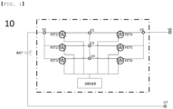
- FIG. 1 is a connection circuit diagram of conventional MOSFETs for vehicles. Power supplied from a vehicle pack BAT is controlled by an apparently single MOSFET. In FIG. 1 , a portion indicated by a dash-single dotted line corresponds to an apparently single MOSFET. Internal FETs shown in FIG. 1 are connected to each other so as to have a 2S3P structure as an example. However, change to various other combinations is possible.
- FET1 to FET6 indicate six internal FETs.
- An N-type MOSFET or a P-type MOSFET is possible as needed.
- only N-type MOSFETs are shown; however, substitution of P-type MOSFETs for N-type MOSFETs is easily selectable as needed.
- FET1, FET2, and FET3 are operated differently from FET4, FET5, and FET6.
- current may flow through FET1, FET2, and FET3 in a direction from the battery pack to the vehicle (from the left to the right in FIG. 1 ).
- current flows through diodes in a direction from the vehicle to the battery pack (from the right to the left in FIG. 1 ).
- current may flow through FET4, FET5, and FET6 in the direction from the vehicle to the battery pack, in contrast to FET1, FET2, and FET3.
- current flows through diodes in the direction from the battery pack to the vehicle.
- the conventional MOSFETs of FIG. 1 are all controlled by a single driver at once.
- the reason that V2, V3, and V4 are connected to each other in FIG. 1 is that, in the case in which a large amount of current instantaneously flows due to abrupt acceleration or abruption braking of a vehicle, it is necessary to distribute the current to a plurality of internal FETs.
- the conventional MOSFETs for vehicles are simultaneously turned ON/OFF by a single driver, and there is no method of diagnosing an error of some of the internal FETs.
- Patent Documents 1 to 3 have something in common in that these documents relate to technologies for diagnosing failure of a plurality of FETs connected to each other in parallel.
- Patent Document 1 In concrete construction, the construction of Patent Document 1 is complicated in that a voltage value of individually detected resistance of a mirror FET provided at each FET is used and additional maintenance of each individual mirror FET is necessary.
- Patent Document 2 is partially similar to the above patent document in that a change in voltage value of a load side terminal, i.e. the final output, generated by controlling ON/OFF of a plurality of FETs is measured to diagnose failure. In Patent Document 2, however, no separate power source for detection is used, and therefore a current measurement means necessary for high voltage must be separately provided. In addition, Patent Document 2 does not suggest a solving means, such as a concrete circuit.
- Patent Document 3 The construction of Patent Document 3 is complicated in that driving of all FETs is individually controlled, in that a separate resistor for current detection is added to each of the FETs, and in that a plurality of parts is added for maintenance thereof. In addition, failure of the diagnosis circuits themselves may become an issue.
- Patent Document 3 Korean Patent Application Publication No. 2016-0041495 (Patent Document 3) relates to detection of faults in MOSFET switching apparatus by detecting excessive current flowing through MOSFET devices.
- US2019/293710 relates to detection of faults in transistor circuits based on impedance.
- JP2001 174531 relates to detecting faults in transistor circuits connecting a battery to a load.
- the present invention has been made in view of the above problems, and it is an object of the present invention to provide a circuit capable of individually diagnosing abnormality of a plurality of internal FETs constituting a MOSFET provided between a secondary battery pack and an electric vehicle having the secondary battery pack therein and a method of diagnosing abnormality of the internal FETs using the same.
- the present invention provides a MOSFET assembly according to claim 1.
- the MOSFET assembly according to the present invention may further include an additional parallel connection including a switch provided between the positive (+) terminal of the secondary battery pack and the vehicle configured to receive the power from the secondary battery pack.
- the MOSFET assembly may be configured such that two MOSFETs are connected to each other in series and two or more pairs of two MOSFETs connected to each other in series are connected to each other in parallel.
- MOSFETs disposed on the battery pack side among the two MOSFETs connected to each other in series, may be operated such that, in the case in which voltage is applied to gates, current flows in a direction from the battery pack to the vehicle, and may be provided with diodes configured to allow current to flow therethrough in a direction from the vehicle to the battery pack in the case in which no voltage is applied to the gates.
- MOSFETs disposed on the vehicle side among the two MOSFETs connected to each other in series, may be operated such that, in the case in which voltage is applied to gates, current flows in the direction from the vehicle to the battery pack, and may be provided with diodes configured to allow current to flow therethrough in the direction from the battery pack to the vehicle in the case in which no voltage is applied to the gates.
- the MOSFETs disposed on the battery pack side and the vehicle side may be symmetric with each other.
- the diodes may be separately connected diodes or parasitic diodes disposed in the MOSFETs.
- the MOSFET assembly may be constituted by an apparently single MOSFET, and the MOSFET assembly may be controlled by a battery management system (BMS) of the secondary battery pack.
- BMS battery management system
- the present invention provides a method of determining abnormality of individual MOSFETs using the MOSFET assembly, the method including measuring voltage at both ends of each individual MOSFET while sequentially turning ON/OFF the channels of the MUX.
- the method may further include measuring voltage at both ends of all individual MOSFETs.
- the MOSFET assembly may be configured such that two MOSFETs are connected to each other in series and two or more pairs of two MOSFETs connected to each other in series are connected to each other in parallel, and the method may further include determining abnormality of MOSFETs disposed on the battery pack side, among the two MOSFETs connected to each other in series, using current supplied from the battery pack.
- the present invention provides a method of determining abnormality of individual MOSFETs using the MOSFET assembly further including an additional parallel connection including a switch provided between the positive (+) terminal of the secondary battery pack and the vehicle configured to receive the power from the secondary battery pack, the method including 1) turning the switch OFF, 2) measuring voltage at both ends of each individual MOSFET while sequentially turning ON/OFF only channels configured to control MOSFETs disposed on the battery pack side, among the channels of the MUX, 3) turning the switch ON, and 4) measuring voltage at both ends of each individual MOSFET while sequentially turning ON/OFF only channels configured to control MOSFETs disposed on the vehicle side, among the channels of the MUX.
- the method may further include measuring voltage at both ends of all individual MOSFETs in each of step 2) and step 4).
- the method may further include comparing values of the voltage at both ends of all of the MOSFETs with each other to determine abnormality of the individual MOSFETs.
- the present invention may be provided in the state in which arbitrary combinations of the above invention are possible.
- FIG. 2 is a partial modification of the connection circuit diagram of the conventional MOSFETs for vehicles.
- connection circuit diagram of the conventional MOSFETs for vehicles is changed in order to determine abnormality of individual MOSFETs.
- V2, V3, and V4 are connected to each other.
- V2, V3, and V4 are short-circuited, whereby the connection circuit diagram of the MOSFETs is changed such that two individual MOSFETs are connected to each other in series and a plurality of pairs of two individual MOSFETs is connected to each other in parallel.
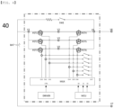
- FIG. 3 is a connection circuit diagram of MOSFETs for vehicles according to a first embodiment of the present invention
- FIG. 4 is a connection circuit diagram of MOSFETs for vehicles according to a second embodiment of the present invention.
- the present invention will be described with reference to FIGS. 3 and 4 .
- FET indicates a MOSFET for power supply.
- the present invention relates to a MOSFET assembly configured such that a plurality of MOSFETs (FET1 to FET6) configured to control connection between a positive (+) terminal of a secondary battery pack, configured to supply power to a vehicle, and the vehicle, configured to receive the power from the secondary battery pack, is connected to each other in series and in parallel.
- MOSFETs FET1 to FET6
- connection points of the vehicle are denoted by V6 and V7.
- FET1 to FET6 indicate six internal FETs.
- An N-type MOSFET or a P-type MOSFET is possible as needed.
- only N-type MOSFETs are shown; however, substitution of P-type MOSFETs for N-type MOSFETs is easily selectable as needed.
- FET1, FET2, and FET3 are operated differently from FET4, FET5, and FET6.
- current may flow through FET1, FET2, and FET3 in a direction from the battery pack to the vehicle.
- current flows through diodes in a direction from the vehicle to the battery pack.
- current may flow through FET4, FET5, and FET6 in the direction from the vehicle to the battery pack, in contrast to FET1, FET2, and FET3.
- Six MUXs connected to the gates of the MOSFETs of the MOSFET assembly have a total of six channels CH1, CH2, CH3, CH4, CH5, and CH6, and the channels are controlled by control signals S0, S1, and S2 sent by a microcontroller unit MCU.
- a driver module which is an input end of the MUX, is also connected to the MUX.
- CH7 may be further added to the MUX. In the case in which no diagnosis is performed, normal operation may be performed through CH7, which is capable of collectively controlling all of the FETs, and switches. In FIG. 3 , FET1, FET2, and FET3 may be continuously maintained ON by CH7. At this time, the other channels, i.e. CH1 to CH6, are OFF.
- MOSFET assembly two MOSFETs are connected to each other in series, and two or more pairs of two MOSFETs connected to each other in series are connected to each other in parallel.
- Diodes configured to allow current to flow therethrough in the direction from the vehicle to the battery pack in the case in which no voltage is applied to the gates, are provided at the MOSFETs (FET1, FET2, and FET3) disposed on the battery pack side, among the two MOSFETs connected to each other in series.
- Diodes configured to allow current to flow therethrough in the direction from the battery pack to the vehicle in the case in which no voltage is applied to the gates, are provided at the MOSFETs (FET4, FET5, and FET6) disposed on the vehicle side, among the two MOSFETs connected to each other in series.
- the diodes may be separately connected diodes or parasitic diodes disposed in the MOSFETs.
- a method of determining abnormality of individual MOSFETs using the MOSFET assembly for vehicle according to the first embodiment of the present invention includes: a step of measuring voltage at both ends of each individual MOSFET while sequentially turning ON/OFF the channels of the MUX.
- the method may further include a step of measuring voltage at both ends of all individual MOSFETs.
- the ON channel In the case in which a certain channel is turned ON by the MUX, the ON channel generates a signal, whereby an FET corresponding thereto is operated.
- CH1 In the case in which CH1 is turned ON, voltage is applied only to the gate of FET1.
- each of V1, V2, and V5 is 48 V while each of V3 and V4 is 0 V in the case in which only FET1 is turned ON.
- each of V1, V2, and V5 In the case in which FET1 is continuously maintained ON (fail on or short), each of V1, V2, and V5 is 48 V even though all of the FETs are turned OFF. In the case in which FET1 is continuously maintained OFF (fail off), only V1 is 48 V even though only FET1 is turned ON.
- a diagnosis table for FET1 is shown below.
- connection circuit diagram of MOSFETs for vehicles according to the second embodiment of the present invention further includes an additional parallel connection including a switch SW1 provided between the positive (+) terminal of the secondary battery pack and the vehicle, configured to receive power from the secondary battery pack, compared to the first embodiment.
- the switch SW1 is connected only for diagnosis.
- the method may further include a step of measuring voltage at both ends of all individual MOSFETs in each of step 2) and step 4).
- the ON channel In the case in which a certain channel is turned ON by the MUX, the ON channel generates a signal, whereby an FET corresponding thereto is operated.
- CH1 In the case in which CH1 is turned ON, voltage is applied only to the gate of FET1.
- each of V1, V2, and V5 is 48 V while each of V3 and V4 is 0 V in the case in which only FET1 is turned ON.
- each of V1, V2, and V5 In the case in which FET1 is continuously maintained ON (fail on or short), each of V1, V2, and V5 is 48 V even though all of the FETs are turned OFF. In the case in which FET1 is continuously maintained OFF (fail off), only V1 is 48 V even though only FET1 is turned ON.
- FIGS. 3 and 4 diagrammatically show two series connections and three parallel connections thereof.
- a plurality of series connections is used instead of the two series connections, however, the solution principle of the present invention is equally applicable, and therefore the above structure must also be included in the scope of right of the present invention.
- the present invention has an advantage in that, in an electric vehicle having a secondary battery pack, it is possible to individually diagnose abnormality of a plurality of internal FETs constituting a MOSFET provided between the secondary battery pack and the electric vehicle. As a result, the present invention is capable of providing a power system having higher safety than a conventional MOSFET assembly.
Landscapes
- Engineering & Computer Science (AREA)
- Physics & Mathematics (AREA)
- General Physics & Mathematics (AREA)
- Microelectronics & Electronic Packaging (AREA)
- Electrochemistry (AREA)
- General Chemical & Material Sciences (AREA)
- Chemical Kinetics & Catalysis (AREA)
- Chemical & Material Sciences (AREA)
- Manufacturing & Machinery (AREA)
- Automation & Control Theory (AREA)
- Human Computer Interaction (AREA)
- Transportation (AREA)
- Mechanical Engineering (AREA)
- Charge And Discharge Circuits For Batteries Or The Like (AREA)
- Secondary Cells (AREA)
- Electronic Switches (AREA)
Claims (13)
- MOSFET-Anordnung, welche eine Mehrzahl an MOSFET umfasst, welche dazu eingerichtet sind, eine Verbindung zwischen einem positiven (+) Anschluss eines Sekundärbatteriepacks zu steuern, welcher dazu verwendet wird, einem Fahrzeug Leistung zuliefern, und das Fahrzeug dazu verwendet wird, die Leistung von dem Sekundärbatteriepack zu empfangen, wobei die Mehrzahl an MOSFET miteinander in Serie und parallel verbunden sind, wobei die MOSFET-Anordnung umfasst:einen MUX, welcher Kanäle aufweist, welche mit Gates der MOSFET der MOSFET-Anordnung verbunden sind,ein Antriebsmodul, welches ein Eingabeende des MUXs ist; undeine Microcontrollereinheit, welche dazu eingerichtet ist, Eingaben bereitzustellen, welche einer gesamten Anzahl der Kanäle entsprechen, welche notwendig sind, den MUX zu steuern, wobeider Microcontroller in Verwendung dazu eingerichtet ist, jeden der Kanäle des MUXs sequenziell an und auszuschalten, während die Spannung an beiden Enden jedes einzelnen MOSFETs gemessen ist.
- MOSFET-Anordnung nach Anspruch 1, welche ferner eine zusätzliche parallele Verbindung umfasst, welche einen Schalter umfasst, welcher zwischen dem positiven (+) Anschluss des Sekundärbatteriepacks und dem Fahrzeug positioniert ist, welches verwendet wird, die Leistung von dem Sekundärbatteriepack zu empfangen.
- MOSFET-Anordnung nach Anspruch 1 oder 2, wobei die MOSFET-Anordnung derart eingerichtet ist, dass zwei MOSFET miteinander in Serie verbunden sind, und zwei oder mehr Paare der zwei MOSFET, welche in Serie miteinander verbunden sind, miteinander parallel verbunden sind.
- MOSFET-Anordnung nach Anspruch 3, wobei MOSFET, welche an der Batteriepackseite angeordnet sind, darunter die zwei MOSFET, welche miteinander in Serie verbunden sind, derart betrieben sind, dass, in einem Fall, in welchem Spannung auf Gates angewandt ist, Strom in einer Richtung von dem Batteriepack zu dem Fahrzeug fließt, und mit Dioden versehen sind, welche dazu eingerichtet sind, es zu ermöglichen, dass Strom dort hindurch in einer Richtung von dem Fahrzeug zu dem Batteriepack fließt, in einem Fall, in welchem keine Spannung auf die Gates angewandt ist, und
MOSFET, welche an der Fahrzeugseite angeordnet sind, darunter die zwei MOSFET, welche miteinander in Serie verbunden sind, derart betrieben sind, dass, in einem Fall, in welchem Spannung auf Gates angewandt ist, Strom in der Richtung von dem Fahrzeug zu dem Batteriepack fließt, und mit Dioden versehen sind, welche dazu eingerichtet sind, es zu ermöglichen, dass Strom dort hindurch in der Richtung von dem Batteriepack zu dem Fahrzeug fließt, in einem Fall, in welchem keine Spannung auf die Gates angewandt ist. - MOSFET-Anordnung nach Anspruch 4, wobei die Dioden separat verbundene Dioden oder parasitäre Dioden sind, welche in den MOSFET angeordnet sind.
- MOSFET-Anordnung nach Anspruch 1 oder 2, wobei die MOSFET-Anordnung durch ein scheinbar einzelnes MOSFET gebildet ist.
- MOSFET-Anordnung nach Anspruch 1 oder 2, wobei die MOSFET-Anordnung durch ein Batterie-Management-System (BMS) des Sekundärbatteriepacks gesteuert ist.
- Verfahren eines Bestimmens einer Abnormalität von individuellen MOSFET unter Verwendung der MOSFET-Anordnung nach Anspruch 1, wobei das Verfahren umfasst:
Messen einer Spannung an beiden Enden jedes individuellen MOSFETs, während sequenziellem An-/Ausschalten der Kanäle des MUXs. - Verfahren eines Bestimmens einer Abnormalität von individuellen MOSFET unter Verwendung der MOSFET-Anordnung nach Anspruch 2, wobei das Verfahren umfasst:1) Ausschalten des Schalters;2) Messen einer Spannung an beiden Enden jedes individuellen MOSFETs, während sequenziellem An-/Ausschalten nur von Kanälen, welche dazu eingerichtet sind, MOSFET zu steuern, welche an der Batteriepackseite angeordnet sind, unter den Kanälen des MUX;3) Anschalten des Schalters; und4) Messen einer Spannung an beiden Enden jedes individuellen MOSFETs, während sequenziellem An-/Ausschalten nur von Kanälen, welche dazu eingerichtet sind, MOSFET zu steuern, welche an der Fahrzeugseite angeordnet sind, unter den Kanälen des MUX.
- Verfahren nach Anspruch 8, welches ferner ein Messen einer Spannung an beiden Enden aller individueller MOSFET umfasst.
- Verfahren nach Anspruch 9, welches ferner ein Messen einer Spannung an beiden Enden aller individueller MOSFET in jedem aus Schritt 2) und Schritt 4) umfasst.
- Verfahren nach Anspruch 8 oder 9, welches ferner ein miteinander Vergleichen von Werten der Spannung an beiden Enden von allen der MOSFET umfasst, um eine Abnormalität der individuellen MOSFET zu bestimmen.
- Verfahren nach Anspruch 8, wobeidie MOSFET-Anordnung derart eingerichtet ist, dass zwei MOSFET miteinander in Serie verbunden sind, und zwei oder mehr Paare der zwei MOSFET, welche in Serie miteinander verbunden sind, miteinander parallel verbunden sind, unddas Verfahren ferner ein Bestimmen einer Abnormalität von MOSFET umfasst, welche an der Batteriepackseite angeordnet sind, darunter die zwei MOSFET, welche miteinander in Serie verbunden sind, unter Verwendung von Strom, welcher von dem Batteriepack geliefert wird.
Applications Claiming Priority (4)
| Application Number | Priority Date | Filing Date | Title |
|---|---|---|---|
| KR20190150213 | 2019-11-21 | ||
| KR20190150214 | 2019-11-21 | ||
| KR1020200155900A KR102827948B1 (ko) | 2019-11-21 | 2020-11-19 | Mux를 포함하는 병렬구조 mosfet의 진단회로 및 이를 이용한 진단방법 |
| PCT/KR2020/016493 WO2021101322A1 (ko) | 2019-11-21 | 2020-11-20 | Mux를 포함하는 병렬구조 mosfet의 진단회로 및 이를 이용한 진단방법 |
Publications (3)
| Publication Number | Publication Date |
|---|---|
| EP4006560A1 EP4006560A1 (de) | 2022-06-01 |
| EP4006560A4 EP4006560A4 (de) | 2022-09-28 |
| EP4006560B1 true EP4006560B1 (de) | 2024-08-14 |
Family
ID=75981384
Family Applications (1)
| Application Number | Title | Priority Date | Filing Date |
|---|---|---|---|
| EP20889077.2A Active EP4006560B1 (de) | 2019-11-21 | 2020-11-20 | Diagnoseschaltung für parallel-struktur-mosfets mit mux und diagnoseverfahren damit |
Country Status (7)
| Country | Link |
|---|---|
| US (1) | US12061224B2 (de) |
| EP (1) | EP4006560B1 (de) |
| JP (1) | JP7643656B2 (de) |
| CN (1) | CN114375403B (de) |
| ES (1) | ES2989488T3 (de) |
| HU (1) | HUE068598T2 (de) |
| WO (1) | WO2021101322A1 (de) |
Families Citing this family (2)
| Publication number | Priority date | Publication date | Assignee | Title |
|---|---|---|---|---|
| JP7420770B2 (ja) | 2021-07-07 | 2024-01-23 | 矢崎総業株式会社 | 電源制御装置および半導体故障検出方法 |
| US12472890B2 (en) | 2023-03-09 | 2025-11-18 | Ford Global Technologies, Llc | Vehicular electrical system sharing primary power with upfit equipment |
Family Cites Families (24)
| Publication number | Priority date | Publication date | Assignee | Title |
|---|---|---|---|---|
| JPS53129249A (en) | 1977-04-18 | 1978-11-11 | Union Carbide Corp | Low energy recovery blending and molding apparatus for plastic material |
| JP2000245054A (ja) | 1999-02-21 | 2000-09-08 | Yazaki Corp | 通電不良判定装置 |
| JP2000293201A (ja) | 1999-04-08 | 2000-10-20 | Nissan Motor Co Ltd | 故障検出装置 |
| JP2001174531A (ja) | 1999-12-15 | 2001-06-29 | Denso Corp | 組電池の異常検出装置 |
| JP4776368B2 (ja) | 2005-12-20 | 2011-09-21 | 矢崎総業株式会社 | 電力供給回路のオン故障検出装置 |
| JP5032378B2 (ja) | 2008-03-31 | 2012-09-26 | セイコーインスツル株式会社 | 充放電制御回路及びバッテリ装置 |
| JP5526965B2 (ja) | 2010-04-15 | 2014-06-18 | 株式会社オートネットワーク技術研究所 | 電源制御装置及び故障検知方法 |
| JP2012054694A (ja) * | 2010-08-31 | 2012-03-15 | On Semiconductor Trading Ltd | 双方向スイッチおよびそれを用いたスイッチ回路 |
| JP2015095442A (ja) | 2013-11-14 | 2015-05-18 | 株式会社オートネットワーク技術研究所 | スイッチ診断装置、スイッチ回路及びスイッチ診断方法 |
| JP6242183B2 (ja) * | 2013-11-22 | 2017-12-06 | 株式会社メガチップス | 半導体集積回路及び該半導体集積回路の試験方法並びに該半導体集積回路におけるラッシュカレントの抑制方法 |
| EP2919262B1 (de) * | 2014-03-14 | 2022-12-21 | EM Microelectronic-Marin SA | Fehlererkennungsanordnung |
| FR3021823B1 (fr) | 2014-05-27 | 2017-10-20 | Renault Sas | Transistor a effet de champ et dispositif de detection de defaillance associe |
| KR20160041495A (ko) | 2014-10-08 | 2016-04-18 | 주식회사 엘지화학 | 모스펫 스위치 구동 장치의 모스펫 진단 장치 및 방법 |
| DE102014115204B4 (de) * | 2014-10-20 | 2020-08-20 | Infineon Technologies Ag | Testen von Vorrichtungen |
| WO2017030020A1 (ja) * | 2015-08-19 | 2017-02-23 | 日本精工株式会社 | 電子制御装置及びそれを搭載した電動パワーステアリング装置 |
| US10884050B2 (en) * | 2016-06-21 | 2021-01-05 | Psemi Corporation | Test of stacked transistors |
| JP6665757B2 (ja) * | 2016-11-08 | 2020-03-13 | 株式会社デンソー | 電源制御装置、及び電池ユニット |
| JP6494673B2 (ja) | 2017-02-13 | 2019-04-03 | 三菱電機株式会社 | 負荷駆動用の集積回路装置 |
| JP6903951B2 (ja) | 2017-02-28 | 2021-07-14 | 株式会社デンソー | 電源システム |
| KR20190034805A (ko) | 2017-09-25 | 2019-04-03 | 주식회사 만도 | 모터 구동 제어 장치 및 방법 |
| KR102204983B1 (ko) | 2017-09-25 | 2021-01-18 | 주식회사 엘지화학 | 배터리 관리 장치와 이를 포함하는 배터리 팩 및 자동차 |
| KR101957485B1 (ko) * | 2017-11-02 | 2019-03-12 | 현대오트론 주식회사 | 로우 사이드 구동 ic 고장진단 장치 및 방법 |
| JP2019168309A (ja) * | 2018-03-23 | 2019-10-03 | 株式会社東芝 | 集積回路 |
| JP2019187187A (ja) * | 2018-04-17 | 2019-10-24 | 日本電産エレシス株式会社 | インバータ回路の故障診断方法 |
-
2020
- 2020-11-20 US US17/615,184 patent/US12061224B2/en active Active
- 2020-11-20 JP JP2021568793A patent/JP7643656B2/ja active Active
- 2020-11-20 EP EP20889077.2A patent/EP4006560B1/de active Active
- 2020-11-20 ES ES20889077T patent/ES2989488T3/es active Active
- 2020-11-20 CN CN202080063123.3A patent/CN114375403B/zh active Active
- 2020-11-20 HU HUE20889077A patent/HUE068598T2/hu unknown
- 2020-11-20 WO PCT/KR2020/016493 patent/WO2021101322A1/ko not_active Ceased
Also Published As
| Publication number | Publication date |
|---|---|
| EP4006560A4 (de) | 2022-09-28 |
| EP4006560A1 (de) | 2022-06-01 |
| CN114375403A (zh) | 2022-04-19 |
| CN114375403B (zh) | 2025-05-23 |
| ES2989488T3 (es) | 2024-11-26 |
| HUE068598T2 (hu) | 2025-01-28 |
| US20220229104A1 (en) | 2022-07-21 |
| WO2021101322A1 (ko) | 2021-05-27 |
| JP7643656B2 (ja) | 2025-03-11 |
| JP2022533395A (ja) | 2022-07-22 |
| US12061224B2 (en) | 2024-08-13 |
Similar Documents
| Publication | Publication Date | Title |
|---|---|---|
| JP5932569B2 (ja) | 半導体装置及び電池電圧監視装置 | |
| US9977083B2 (en) | Switched high-voltage sampling circuit for electric vehicles | |
| JP4931378B2 (ja) | 車両用の電源装置 | |
| US11843274B2 (en) | Charge control apparatus for controlling charging of an energy storage device via purality of charging paths connected in parallel anssociated energy storage appartus, and an associated charging method | |
| KR20140136844A (ko) | 배터리 팩의 릴레이 진단장치 및 배터리 제어 시스템 | |
| EP4006560B1 (de) | Diagnoseschaltung für parallel-struktur-mosfets mit mux und diagnoseverfahren damit | |
| US10286753B2 (en) | On-state malfunction detection device and method therefor | |
| KR101562016B1 (ko) | 셀 밸런싱 스위치의 고장 진단 장치 및 방법 | |
| US11400824B2 (en) | Electrical propulsion system architecture | |
| CN113196664B (zh) | 用于方向相关地运行电化学能量存储器的设备和方法 | |
| KR20160041495A (ko) | 모스펫 스위치 구동 장치의 모스펫 진단 장치 및 방법 | |
| US20240183911A1 (en) | Anomaly detection apparatus and anomaly detection method | |
| CN111034046A (zh) | 连接单元及电源系统 | |
| KR20140028349A (ko) | 셀 밸런싱 장치 | |
| KR102827948B1 (ko) | Mux를 포함하는 병렬구조 mosfet의 진단회로 및 이를 이용한 진단방법 | |
| KR102765818B1 (ko) | And 게이트를 포함하는 병렬구조 mosfet의 진단회로 및 이를 이용한 진단방법 | |
| KR102753193B1 (ko) | Ldo와 션트 저항을 포함하는 병렬 fet의 진단회로 및 이를 이용한 진단방법 | |
| US20250290982A1 (en) | Relay Diagnosis Apparatus and Battery Pack Including the Same | |
| CN110461637A (zh) | 车辆能量存储器 | |
| JP6264186B2 (ja) | 電池パック | |
| KR102846504B1 (ko) | Mux와 ldo를 포함하는 병렬 fet의 진단회로 및 이를 이용한 진단방법 | |
| JP6658381B2 (ja) | 漏電判定装置 | |
| KR102837603B1 (ko) | 배터리 장치, 스위치 진단 장치 및 방법 | |
| JP7151741B2 (ja) | 電圧検出装置 | |
| KR102954864B1 (ko) | 릴레이의 고장 진단 방법 및 이를 이용하는 배터리 시스템 |
Legal Events
| Date | Code | Title | Description |
|---|---|---|---|
| STAA | Information on the status of an ep patent application or granted ep patent |
Free format text: STATUS: THE INTERNATIONAL PUBLICATION HAS BEEN MADE |
|
| PUAI | Public reference made under article 153(3) epc to a published international application that has entered the european phase |
Free format text: ORIGINAL CODE: 0009012 |
|
| STAA | Information on the status of an ep patent application or granted ep patent |
Free format text: STATUS: REQUEST FOR EXAMINATION WAS MADE |
|
| 17P | Request for examination filed |
Effective date: 20220222 |
|
| AK | Designated contracting states |
Kind code of ref document: A1 Designated state(s): AL AT BE BG CH CY CZ DE DK EE ES FI FR GB GR HR HU IE IS IT LI LT LU LV MC MK MT NL NO PL PT RO RS SE SI SK SM TR |
|
| A4 | Supplementary search report drawn up and despatched |
Effective date: 20220825 |
|
| RIC1 | Information provided on ipc code assigned before grant |
Ipc: H01M 10/42 20060101ALI20220819BHEP Ipc: G01R 31/00 20060101ALI20220819BHEP Ipc: G01R 31/327 20060101ALI20220819BHEP Ipc: G01R 31/26 20200101ALI20220819BHEP Ipc: G01R 31/27 20060101AFI20220819BHEP |
|
| DAV | Request for validation of the european patent (deleted) | ||
| DAX | Request for extension of the european patent (deleted) | ||
| GRAP | Despatch of communication of intention to grant a patent |
Free format text: ORIGINAL CODE: EPIDOSNIGR1 |
|
| STAA | Information on the status of an ep patent application or granted ep patent |
Free format text: STATUS: GRANT OF PATENT IS INTENDED |
|
| INTG | Intention to grant announced |
Effective date: 20240315 |
|
| P01 | Opt-out of the competence of the unified patent court (upc) registered |
Effective date: 20240404 |
|
| GRAS | Grant fee paid |
Free format text: ORIGINAL CODE: EPIDOSNIGR3 |
|
| GRAA | (expected) grant |
Free format text: ORIGINAL CODE: 0009210 |
|
| STAA | Information on the status of an ep patent application or granted ep patent |
Free format text: STATUS: THE PATENT HAS BEEN GRANTED |
|
| AK | Designated contracting states |
Kind code of ref document: B1 Designated state(s): AL AT BE BG CH CY CZ DE DK EE ES FI FR GB GR HR HU IE IS IT LI LT LU LV MC MK MT NL NO PL PT RO RS SE SI SK SM TR |
|
| REG | Reference to a national code |
Ref country code: GB Ref legal event code: FG4D |
|
| REG | Reference to a national code |
Ref country code: CH Ref legal event code: EP |
|
| REG | Reference to a national code |
Ref country code: DE Ref legal event code: R096 Ref document number: 602020035964 Country of ref document: DE |
|
| REG | Reference to a national code |
Ref country code: IE Ref legal event code: FG4D |
|
| REG | Reference to a national code |
Ref country code: ES Ref legal event code: FG2A Ref document number: 2989488 Country of ref document: ES Kind code of ref document: T3 Effective date: 20241126 |
|
| REG | Reference to a national code |
Ref country code: LT Ref legal event code: MG9D |
|
| REG | Reference to a national code |
Ref country code: NL Ref legal event code: MP Effective date: 20240814 |
|
| PG25 | Lapsed in a contracting state [announced via postgrant information from national office to epo] |
Ref country code: NO Free format text: LAPSE BECAUSE OF FAILURE TO SUBMIT A TRANSLATION OF THE DESCRIPTION OR TO PAY THE FEE WITHIN THE PRESCRIBED TIME-LIMIT Effective date: 20241114 |
|
| REG | Reference to a national code |
Ref country code: AT Ref legal event code: MK05 Ref document number: 1713768 Country of ref document: AT Kind code of ref document: T Effective date: 20240814 |
|
| PG25 | Lapsed in a contracting state [announced via postgrant information from national office to epo] |
Ref country code: FI Free format text: LAPSE BECAUSE OF FAILURE TO SUBMIT A TRANSLATION OF THE DESCRIPTION OR TO PAY THE FEE WITHIN THE PRESCRIBED TIME-LIMIT Effective date: 20240814 Ref country code: GR Free format text: LAPSE BECAUSE OF FAILURE TO SUBMIT A TRANSLATION OF THE DESCRIPTION OR TO PAY THE FEE WITHIN THE PRESCRIBED TIME-LIMIT Effective date: 20241115 Ref country code: NL Free format text: LAPSE BECAUSE OF FAILURE TO SUBMIT A TRANSLATION OF THE DESCRIPTION OR TO PAY THE FEE WITHIN THE PRESCRIBED TIME-LIMIT Effective date: 20240814 Ref country code: PT Free format text: LAPSE BECAUSE OF FAILURE TO SUBMIT A TRANSLATION OF THE DESCRIPTION OR TO PAY THE FEE WITHIN THE PRESCRIBED TIME-LIMIT Effective date: 20241216 Ref country code: PL Free format text: LAPSE BECAUSE OF FAILURE TO SUBMIT A TRANSLATION OF THE DESCRIPTION OR TO PAY THE FEE WITHIN THE PRESCRIBED TIME-LIMIT Effective date: 20240814 |
|
| PG25 | Lapsed in a contracting state [announced via postgrant information from national office to epo] |
Ref country code: BG Free format text: LAPSE BECAUSE OF FAILURE TO SUBMIT A TRANSLATION OF THE DESCRIPTION OR TO PAY THE FEE WITHIN THE PRESCRIBED TIME-LIMIT Effective date: 20240814 |
|
| PG25 | Lapsed in a contracting state [announced via postgrant information from national office to epo] |
Ref country code: LV Free format text: LAPSE BECAUSE OF FAILURE TO SUBMIT A TRANSLATION OF THE DESCRIPTION OR TO PAY THE FEE WITHIN THE PRESCRIBED TIME-LIMIT Effective date: 20240814 |
|
| PG25 | Lapsed in a contracting state [announced via postgrant information from national office to epo] |
Ref country code: IS Free format text: LAPSE BECAUSE OF FAILURE TO SUBMIT A TRANSLATION OF THE DESCRIPTION OR TO PAY THE FEE WITHIN THE PRESCRIBED TIME-LIMIT Effective date: 20241214 Ref country code: AT Free format text: LAPSE BECAUSE OF FAILURE TO SUBMIT A TRANSLATION OF THE DESCRIPTION OR TO PAY THE FEE WITHIN THE PRESCRIBED TIME-LIMIT Effective date: 20240814 |
|
| PG25 | Lapsed in a contracting state [announced via postgrant information from national office to epo] |
Ref country code: HR Free format text: LAPSE BECAUSE OF FAILURE TO SUBMIT A TRANSLATION OF THE DESCRIPTION OR TO PAY THE FEE WITHIN THE PRESCRIBED TIME-LIMIT Effective date: 20240814 |
|
| PG25 | Lapsed in a contracting state [announced via postgrant information from national office to epo] |
Ref country code: RS Free format text: LAPSE BECAUSE OF FAILURE TO SUBMIT A TRANSLATION OF THE DESCRIPTION OR TO PAY THE FEE WITHIN THE PRESCRIBED TIME-LIMIT Effective date: 20241114 |
|
| REG | Reference to a national code |
Ref country code: HU Ref legal event code: AG4A Ref document number: E068598 Country of ref document: HU |
|
| PG25 | Lapsed in a contracting state [announced via postgrant information from national office to epo] |
Ref country code: RS Free format text: LAPSE BECAUSE OF FAILURE TO SUBMIT A TRANSLATION OF THE DESCRIPTION OR TO PAY THE FEE WITHIN THE PRESCRIBED TIME-LIMIT Effective date: 20241114 Ref country code: PT Free format text: LAPSE BECAUSE OF FAILURE TO SUBMIT A TRANSLATION OF THE DESCRIPTION OR TO PAY THE FEE WITHIN THE PRESCRIBED TIME-LIMIT Effective date: 20241216 Ref country code: PL Free format text: LAPSE BECAUSE OF FAILURE TO SUBMIT A TRANSLATION OF THE DESCRIPTION OR TO PAY THE FEE WITHIN THE PRESCRIBED TIME-LIMIT Effective date: 20240814 Ref country code: NO Free format text: LAPSE BECAUSE OF FAILURE TO SUBMIT A TRANSLATION OF THE DESCRIPTION OR TO PAY THE FEE WITHIN THE PRESCRIBED TIME-LIMIT Effective date: 20241114 Ref country code: NL Free format text: LAPSE BECAUSE OF FAILURE TO SUBMIT A TRANSLATION OF THE DESCRIPTION OR TO PAY THE FEE WITHIN THE PRESCRIBED TIME-LIMIT Effective date: 20240814 Ref country code: LV Free format text: LAPSE BECAUSE OF FAILURE TO SUBMIT A TRANSLATION OF THE DESCRIPTION OR TO PAY THE FEE WITHIN THE PRESCRIBED TIME-LIMIT Effective date: 20240814 Ref country code: IS Free format text: LAPSE BECAUSE OF FAILURE TO SUBMIT A TRANSLATION OF THE DESCRIPTION OR TO PAY THE FEE WITHIN THE PRESCRIBED TIME-LIMIT Effective date: 20241214 Ref country code: HR Free format text: LAPSE BECAUSE OF FAILURE TO SUBMIT A TRANSLATION OF THE DESCRIPTION OR TO PAY THE FEE WITHIN THE PRESCRIBED TIME-LIMIT Effective date: 20240814 Ref country code: GR Free format text: LAPSE BECAUSE OF FAILURE TO SUBMIT A TRANSLATION OF THE DESCRIPTION OR TO PAY THE FEE WITHIN THE PRESCRIBED TIME-LIMIT Effective date: 20241115 Ref country code: FI Free format text: LAPSE BECAUSE OF FAILURE TO SUBMIT A TRANSLATION OF THE DESCRIPTION OR TO PAY THE FEE WITHIN THE PRESCRIBED TIME-LIMIT Effective date: 20240814 Ref country code: BG Free format text: LAPSE BECAUSE OF FAILURE TO SUBMIT A TRANSLATION OF THE DESCRIPTION OR TO PAY THE FEE WITHIN THE PRESCRIBED TIME-LIMIT Effective date: 20240814 Ref country code: AT Free format text: LAPSE BECAUSE OF FAILURE TO SUBMIT A TRANSLATION OF THE DESCRIPTION OR TO PAY THE FEE WITHIN THE PRESCRIBED TIME-LIMIT Effective date: 20240814 |
|
| PG25 | Lapsed in a contracting state [announced via postgrant information from national office to epo] |
Ref country code: RO Free format text: LAPSE BECAUSE OF FAILURE TO SUBMIT A TRANSLATION OF THE DESCRIPTION OR TO PAY THE FEE WITHIN THE PRESCRIBED TIME-LIMIT Effective date: 20240814 Ref country code: DK Free format text: LAPSE BECAUSE OF FAILURE TO SUBMIT A TRANSLATION OF THE DESCRIPTION OR TO PAY THE FEE WITHIN THE PRESCRIBED TIME-LIMIT Effective date: 20240814 Ref country code: SM Free format text: LAPSE BECAUSE OF FAILURE TO SUBMIT A TRANSLATION OF THE DESCRIPTION OR TO PAY THE FEE WITHIN THE PRESCRIBED TIME-LIMIT Effective date: 20240814 |
|
| PG25 | Lapsed in a contracting state [announced via postgrant information from national office to epo] |
Ref country code: EE Free format text: LAPSE BECAUSE OF FAILURE TO SUBMIT A TRANSLATION OF THE DESCRIPTION OR TO PAY THE FEE WITHIN THE PRESCRIBED TIME-LIMIT Effective date: 20240814 |
|
| PG25 | Lapsed in a contracting state [announced via postgrant information from national office to epo] |
Ref country code: CZ Free format text: LAPSE BECAUSE OF FAILURE TO SUBMIT A TRANSLATION OF THE DESCRIPTION OR TO PAY THE FEE WITHIN THE PRESCRIBED TIME-LIMIT Effective date: 20240814 |
|
| PG25 | Lapsed in a contracting state [announced via postgrant information from national office to epo] |
Ref country code: SK Free format text: LAPSE BECAUSE OF FAILURE TO SUBMIT A TRANSLATION OF THE DESCRIPTION OR TO PAY THE FEE WITHIN THE PRESCRIBED TIME-LIMIT Effective date: 20240814 Ref country code: IT Free format text: LAPSE BECAUSE OF FAILURE TO SUBMIT A TRANSLATION OF THE DESCRIPTION OR TO PAY THE FEE WITHIN THE PRESCRIBED TIME-LIMIT Effective date: 20240814 |
|
| REG | Reference to a national code |
Ref country code: DE Ref legal event code: R097 Ref document number: 602020035964 Country of ref document: DE |
|
| PLBE | No opposition filed within time limit |
Free format text: ORIGINAL CODE: 0009261 |
|
| STAA | Information on the status of an ep patent application or granted ep patent |
Free format text: STATUS: NO OPPOSITION FILED WITHIN TIME LIMIT |
|
| REG | Reference to a national code |
Ref country code: CH Ref legal event code: PL |
|
| PG25 | Lapsed in a contracting state [announced via postgrant information from national office to epo] |
Ref country code: MC Free format text: LAPSE BECAUSE OF FAILURE TO SUBMIT A TRANSLATION OF THE DESCRIPTION OR TO PAY THE FEE WITHIN THE PRESCRIBED TIME-LIMIT Effective date: 20240814 |
|
| PG25 | Lapsed in a contracting state [announced via postgrant information from national office to epo] |
Ref country code: LU Free format text: LAPSE BECAUSE OF NON-PAYMENT OF DUE FEES Effective date: 20241120 |
|
| REG | Reference to a national code |
Ref country code: CH Ref legal event code: PL |
|
| 26N | No opposition filed |
Effective date: 20250515 |
|
| PG25 | Lapsed in a contracting state [announced via postgrant information from national office to epo] |
Ref country code: CH Free format text: LAPSE BECAUSE OF NON-PAYMENT OF DUE FEES Effective date: 20241130 |
|
| PG25 | Lapsed in a contracting state [announced via postgrant information from national office to epo] |
Ref country code: SE Free format text: LAPSE BECAUSE OF FAILURE TO SUBMIT A TRANSLATION OF THE DESCRIPTION OR TO PAY THE FEE WITHIN THE PRESCRIBED TIME-LIMIT Effective date: 20240814 |
|
| PG25 | Lapsed in a contracting state [announced via postgrant information from national office to epo] |
Ref country code: IE Free format text: LAPSE BECAUSE OF NON-PAYMENT OF DUE FEES Effective date: 20241120 |
|
| PGFP | Annual fee paid to national office [announced via postgrant information from national office to epo] |
Ref country code: HU Payment date: 20251127 Year of fee payment: 6 |
|
| PGFP | Annual fee paid to national office [announced via postgrant information from national office to epo] |
Ref country code: DE Payment date: 20251020 Year of fee payment: 6 |
|
| PGFP | Annual fee paid to national office [announced via postgrant information from national office to epo] |
Ref country code: GB Payment date: 20251023 Year of fee payment: 6 |
|
| PGFP | Annual fee paid to national office [announced via postgrant information from national office to epo] |
Ref country code: FR Payment date: 20251021 Year of fee payment: 6 |
|
| PGFP | Annual fee paid to national office [announced via postgrant information from national office to epo] |
Ref country code: BE Payment date: 20251020 Year of fee payment: 6 |
|
| PGFP | Annual fee paid to national office [announced via postgrant information from national office to epo] |
Ref country code: ES Payment date: 20251215 Year of fee payment: 6 |
|
| PG25 | Lapsed in a contracting state [announced via postgrant information from national office to epo] |
Ref country code: CY Free format text: LAPSE BECAUSE OF FAILURE TO SUBMIT A TRANSLATION OF THE DESCRIPTION OR TO PAY THE FEE WITHIN THE PRESCRIBED TIME-LIMIT; INVALID AB INITIO Effective date: 20201120 |