EP4002611A1 - Q-schaltresonator und impulsgenerator - Google Patents
Q-schaltresonator und impulsgenerator Download PDFInfo
- Publication number
- EP4002611A1 EP4002611A1 EP20841644.6A EP20841644A EP4002611A1 EP 4002611 A1 EP4002611 A1 EP 4002611A1 EP 20841644 A EP20841644 A EP 20841644A EP 4002611 A1 EP4002611 A1 EP 4002611A1
- Authority
- EP
- European Patent Office
- Prior art keywords
- resonator
- optical
- switch
- pulse
- optical resonator
- Prior art date
- Legal status (The legal status is an assumption and is not a legal conclusion. Google has not performed a legal analysis and makes no representation as to the accuracy of the status listed.)
- Pending
Links
Images


Classifications
-
- G—PHYSICS
- G02—OPTICS
- G02F—OPTICAL DEVICES OR ARRANGEMENTS FOR THE CONTROL OF LIGHT BY MODIFICATION OF THE OPTICAL PROPERTIES OF THE MEDIA OF THE ELEMENTS INVOLVED THEREIN; NON-LINEAR OPTICS; FREQUENCY-CHANGING OF LIGHT; OPTICAL LOGIC ELEMENTS; OPTICAL ANALOGUE/DIGITAL CONVERTERS
- G02F1/00—Devices or arrangements for the control of the intensity, colour, phase, polarisation or direction of light arriving from an independent light source, e.g. switching, gating or modulating; Non-linear optics
- G02F1/01—Devices or arrangements for the control of the intensity, colour, phase, polarisation or direction of light arriving from an independent light source, e.g. switching, gating or modulating; Non-linear optics for the control of the intensity, phase, polarisation or colour
- G02F1/03—Devices or arrangements for the control of the intensity, colour, phase, polarisation or direction of light arriving from an independent light source, e.g. switching, gating or modulating; Non-linear optics for the control of the intensity, phase, polarisation or colour based on ceramics or electro-optical crystals, e.g. exhibiting Pockels effect or Kerr effect
-
- H—ELECTRICITY
- H01—ELECTRIC ELEMENTS
- H01S—DEVICES USING THE PROCESS OF LIGHT AMPLIFICATION BY STIMULATED EMISSION OF RADIATION [LASER] TO AMPLIFY OR GENERATE LIGHT; DEVICES USING STIMULATED EMISSION OF ELECTROMAGNETIC RADIATION IN WAVE RANGES OTHER THAN OPTICAL
- H01S3/00—Lasers, i.e. devices using stimulated emission of electromagnetic radiation in the infrared, visible or ultraviolet wave range
- H01S3/10—Controlling the intensity, frequency, phase, polarisation or direction of the emitted radiation, e.g. switching, gating, modulating or demodulating
- H01S3/10007—Controlling the intensity, frequency, phase, polarisation or direction of the emitted radiation, e.g. switching, gating, modulating or demodulating in optical amplifiers
-
- G—PHYSICS
- G02—OPTICS
- G02B—OPTICAL ELEMENTS, SYSTEMS OR APPARATUS
- G02B26/00—Optical devices or arrangements for the control of light using movable or deformable optical elements
- G02B26/02—Optical devices or arrangements for the control of light using movable or deformable optical elements for controlling the intensity of light
-
- G—PHYSICS
- G02—OPTICS
- G02F—OPTICAL DEVICES OR ARRANGEMENTS FOR THE CONTROL OF LIGHT BY MODIFICATION OF THE OPTICAL PROPERTIES OF THE MEDIA OF THE ELEMENTS INVOLVED THEREIN; NON-LINEAR OPTICS; FREQUENCY-CHANGING OF LIGHT; OPTICAL LOGIC ELEMENTS; OPTICAL ANALOGUE/DIGITAL CONVERTERS
- G02F1/00—Devices or arrangements for the control of the intensity, colour, phase, polarisation or direction of light arriving from an independent light source, e.g. switching, gating or modulating; Non-linear optics
- G02F1/01—Devices or arrangements for the control of the intensity, colour, phase, polarisation or direction of light arriving from an independent light source, e.g. switching, gating or modulating; Non-linear optics for the control of the intensity, phase, polarisation or colour
- G02F1/11—Devices or arrangements for the control of the intensity, colour, phase, polarisation or direction of light arriving from an independent light source, e.g. switching, gating or modulating; Non-linear optics for the control of the intensity, phase, polarisation or colour based on acousto-optical elements, e.g. using variable diffraction by sound or like mechanical waves
-
- G—PHYSICS
- G02—OPTICS
- G02F—OPTICAL DEVICES OR ARRANGEMENTS FOR THE CONTROL OF LIGHT BY MODIFICATION OF THE OPTICAL PROPERTIES OF THE MEDIA OF THE ELEMENTS INVOLVED THEREIN; NON-LINEAR OPTICS; FREQUENCY-CHANGING OF LIGHT; OPTICAL LOGIC ELEMENTS; OPTICAL ANALOGUE/DIGITAL CONVERTERS
- G02F1/00—Devices or arrangements for the control of the intensity, colour, phase, polarisation or direction of light arriving from an independent light source, e.g. switching, gating or modulating; Non-linear optics
- G02F1/35—Non-linear optics
- G02F1/3523—Non-linear absorption changing by light, e.g. bleaching
-
- H—ELECTRICITY
- H01—ELECTRIC ELEMENTS
- H01S—DEVICES USING THE PROCESS OF LIGHT AMPLIFICATION BY STIMULATED EMISSION OF RADIATION [LASER] TO AMPLIFY OR GENERATE LIGHT; DEVICES USING STIMULATED EMISSION OF ELECTROMAGNETIC RADIATION IN WAVE RANGES OTHER THAN OPTICAL
- H01S3/00—Lasers, i.e. devices using stimulated emission of electromagnetic radiation in the infrared, visible or ultraviolet wave range
- H01S3/10—Controlling the intensity, frequency, phase, polarisation or direction of the emitted radiation, e.g. switching, gating, modulating or demodulating
- H01S3/11—Mode locking; Q-switching; Other giant-pulse techniques, e.g. cavity dumping
- H01S3/1123—Q-switching
- H01S3/113—Q-switching using intracavity saturable absorbers
-
- H—ELECTRICITY
- H01—ELECTRIC ELEMENTS
- H01S—DEVICES USING THE PROCESS OF LIGHT AMPLIFICATION BY STIMULATED EMISSION OF RADIATION [LASER] TO AMPLIFY OR GENERATE LIGHT; DEVICES USING STIMULATED EMISSION OF ELECTROMAGNETIC RADIATION IN WAVE RANGES OTHER THAN OPTICAL
- H01S3/00—Lasers, i.e. devices using stimulated emission of electromagnetic radiation in the infrared, visible or ultraviolet wave range
- H01S3/10—Controlling the intensity, frequency, phase, polarisation or direction of the emitted radiation, e.g. switching, gating, modulating or demodulating
- H01S3/11—Mode locking; Q-switching; Other giant-pulse techniques, e.g. cavity dumping
- H01S3/1123—Q-switching
- H01S3/117—Q-switching using intracavity acousto-optic devices
-
- H—ELECTRICITY
- H01—ELECTRIC ELEMENTS
- H01S—DEVICES USING THE PROCESS OF LIGHT AMPLIFICATION BY STIMULATED EMISSION OF RADIATION [LASER] TO AMPLIFY OR GENERATE LIGHT; DEVICES USING STIMULATED EMISSION OF ELECTROMAGNETIC RADIATION IN WAVE RANGES OTHER THAN OPTICAL
- H01S3/00—Lasers, i.e. devices using stimulated emission of electromagnetic radiation in the infrared, visible or ultraviolet wave range
- H01S3/10—Controlling the intensity, frequency, phase, polarisation or direction of the emitted radiation, e.g. switching, gating, modulating or demodulating
- H01S3/11—Mode locking; Q-switching; Other giant-pulse techniques, e.g. cavity dumping
- H01S3/1123—Q-switching
- H01S3/121—Q-switching using intracavity mechanical devices
-
- H—ELECTRICITY
- H01—ELECTRIC ELEMENTS
- H01S—DEVICES USING THE PROCESS OF LIGHT AMPLIFICATION BY STIMULATED EMISSION OF RADIATION [LASER] TO AMPLIFY OR GENERATE LIGHT; DEVICES USING STIMULATED EMISSION OF ELECTROMAGNETIC RADIATION IN WAVE RANGES OTHER THAN OPTICAL
- H01S5/00—Semiconductor lasers
- H01S5/02—Structural details or components not essential to laser action
- H01S5/022—Mountings; Housings
- H01S5/02208—Mountings; Housings characterised by the shape of the housings
-
- H—ELECTRICITY
- H01—ELECTRIC ELEMENTS
- H01S—DEVICES USING THE PROCESS OF LIGHT AMPLIFICATION BY STIMULATED EMISSION OF RADIATION [LASER] TO AMPLIFY OR GENERATE LIGHT; DEVICES USING STIMULATED EMISSION OF ELECTROMAGNETIC RADIATION IN WAVE RANGES OTHER THAN OPTICAL
- H01S5/00—Semiconductor lasers
- H01S5/06—Arrangements for controlling the laser output parameters, e.g. by operating on the active medium
- H01S5/065—Mode locking; Mode suppression; Mode selection ; Self pulsating
- H01S5/0651—Mode control
-
- G—PHYSICS
- G02—OPTICS
- G02F—OPTICAL DEVICES OR ARRANGEMENTS FOR THE CONTROL OF LIGHT BY MODIFICATION OF THE OPTICAL PROPERTIES OF THE MEDIA OF THE ELEMENTS INVOLVED THEREIN; NON-LINEAR OPTICS; FREQUENCY-CHANGING OF LIGHT; OPTICAL LOGIC ELEMENTS; OPTICAL ANALOGUE/DIGITAL CONVERTERS
- G02F2203/00—Function characteristic
- G02F2203/52—Optical limiters
Definitions
- the present invention relates to a Q switch resonator and a pulse generator.
- a Q-switch laser is a pulse laser configured to convert energy accumulated as a population inversion in a gain medium into an optical pulse having high energy by switching a Q factor of a laser resonator from low to high and to output the optical pulse. While the population inversion is being created in the gain medium in the resonator, the Q factor is maintained low in order to prevent laser oscillation and loss of the population inversion. When a sufficiently large population inversion is reached in the gain medium, the Q factor is increased to cause pulse oscillation.
- a Q-switch carbon dioxide gas laser (for example, see JP H8-64897 A ) using carbon dioxide gas as a gain medium, a solid state laser device (for example, see JP H4-171780 A ) using a neodymium doped YAG crystal, and the like have been known.
- CW continuous wave
- intermittent CW laser having high average power
- semiconductor lasers being small and inexpensive, having low power consumption, and being configured to oscillate at a desired wavelength, have been widely used.
- a laser with a short excitation life such as a semiconductor laser, cannot sufficiently store energy and is not suitable for normal Q switch pulse oscillation. Also, in terms of light damage to a laser medium, it is difficult to extract an optical pulse having high peak power. An efficient pulse-extraction configuration is desired.
- An object of the present invention is to provide a Q switch resonator that achieves efficient pulse extraction, and a pulse generator using the Q switch resonator.
- An optical resonator is used separately from a laser medium, light is accumulated in the resonator, and a Q factor is switched from a high value to a low value to output an optical pulse.
- a Q switch resonator in a first aspect of the present invention, includes an optical resonator formed of at least two mirrors, and configured to accumulate power of a continuous wave or an intermittent continuous wave incident from an outside, and a switching element provided in the optical resonator.
- the switching element When the power accumulated in the optical resonator increases to a predetermined level, the switching element outputs an optical pulse by lowering a Q factor from a first level to a second level lower than the first level.
- a pulse generator in a second aspect of the present invention, includes a first optical resonator, and a light source configured to cause a continuous wave or an intermittent continuous wave to be incident on the first optical resonator.
- the first optical resonator includes a first switching element, and, when power of light incident on the first optical resonator increases to a predetermined level, the first switching element outputs an optical pulse by lowering a Q factor of the first optical resonator from a first level to a second level lower than the first level.
- a pulse output having high peak power is generated by externally pulsing an output of a CW laser (including an intermittent CW laser).
- a resonator is provided separately from the laser, light is accumulated in the resonator, and a Q factor of the resonator is switched from a high value to a low value to output a pulse having high energy.
- FIG. 1 is a basic configuration diagram of the present invention.
- a pulse generator 1 includes a CW laser 31 as a light source, and a Q switch resonator 10.
- the CW laser 31 is configured to output a continuous wave or an intermittent continuous wave.
- the continuous wave or the intermittent continuous wave output from the CW laser 31 is incident on the Q switch resonator 10 and amplified.
- the Q switch resonator 10 includes at least two mirrors 11 and 12, and a Q switch 15 being a switching element.
- the mirror 11 and the mirror 12 form an optical resonator.
- the Q switch resonator 10 does not contain a laser medium or a gain medium in the resonator.
- the incident continuous wave or intermittent continuous wave from the outside is repeatedly reflected and amplified between the mirror 11 and the mirror 12, and light energy is accumulated in the optical resonator. While the light energy is accumulated, a Q factor of the resonator is maintained high. When the power accumulated in the resonator becomes equal to or higher than a certain level, the Q factor is switched to a low side to release the accumulated power.
- the Q factor is a dimensionless amount representing a continuous characteristic of oscillation of a resonant system, and is generally expressed in a ratio of an oscillation frequency to a line width (a full width half maximum (FWHM)) of a resonant frequency.
- FWHM full width half maximum
- the Q switch 15 releases energy at once to reduce the Q factor.
- an optical pulse having high energy is output from the resonator.
- This configuration is fundamentally different from a configuration of a general Q switch laser, i.e., a configuration in which a Q factor is maintained low while light energy is being accumulated in a gain medium, and the Q factor is increased for oscillation when the energy has been stored.
- FIGS. 2A to 2C are diagrams illustrating principles of the present invention.
- CW light or intermittent CW light incident on an optical resonator 110 from the outside is repeatedly reflected between the mirror 11 and the mirror 12 multiple times (S1).
- S1 CW light or intermittent CW light
- FIG. 2B an increase in the number of repetitions of reflection of the light between the mirror 11 and the mirror 12 causes an increase in energy accumulated in the optical resonator 110 (S2).
- FIG. 2C when the energy in the optical resonator 110 becomes sufficiently high, the Q factor is switched from high to low to release an optical pulse (S3).
- FIGS. 3A to 3C are graphs illustrating characteristics of the optical resonator 110.
- the CW light is incident at time 0, an optical pulse is output at time t1.
- the Q factor is maintained high until the time t1. Accordingly, the light stably repeatedly reflects or oscillates in the optical resonator 110.
- the Q factor is switched to zero.
- FIG. 3B shows a profile of power in the resonator. Energy is gradually accumulated in the resonator from the incidence of the CW light until the time t1.
- the origin corresponds to S1 in FIG. 2A
- the process of power increase corresponds to S2 in FIG. 2B .
- the power reaches a constant level at the time t1, the power decreases at once by switching of the Q switch 15. This point in time corresponds to S3 in FIG. 2C .
- FIG. 3C shows a profile of output power. There is no output from the resonator until the time t1, and a sharp short pulse is output at the time t1.
- a gain medium is not disposed in the resonator, and thus the problem of light damage is avoided.
- Sufficient energy can be accumulated in the optical resonator 110 by repeated reflection of the light between the mirror 11 and the mirror 12, and an optical pulse having high peak power can be extracted.
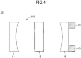
- FIG. 4 is a schematic diagram of the Q switch resonator 10 according to a first embodiment.
- the Q switch resonator 10 includes the mirror 11 and the mirror 12 that constitute the optical resonator 110, and the Q switch 15. At least one of the mirror 11 and the mirror 12 may be provided with an actuator 13 for adjusting a resonator length.
- the mirror 11 and the mirror 12 are disposed such that light having made a round-trip in the resonator overlaps an original optical path.
- a power transmittance of the light when having made a round-trip in the resonator is A RT .
- f represents a center frequency of a frequency spectrum
- ⁇ f represents an FWHM of the frequency spectrum
- F represents a finesse, which is a resolution of the frequency spectrum
- L is a length of a single round-trip of the resonator
- ⁇ is a wavelength of the light.
- the finesse F is defined as F ⁇ ⁇ (A RT ) 0.25 /[1 - (A RT ) 0.5 ].
- the actuator 13 is used to set a resonator length in a single round-trip to be an integral multiple of the wavelength ⁇ of the light.
- a piezoelectric element or the like for example, can be used for the actuator 13.
- the Q switch 15 is provided in the optical resonator 110.
- the Q switch 15 is used to control the finesse F by changing an attenuation, i.e., a transmittance A Q of the light, and is also used to extract an optical pulse.
- a response speed ⁇ Q and a maximum transmittance A Q mAx have great significance.
- the response speed ⁇ Q is preferably faster, and the maximum transmittance A Q MAX is preferably higher.
- FIGS. 5A to 5C are configuration examples of the Q switch 15.
- a Q switch resonator 10A in FIG. 5A uses a mechanical Q switch 15a.
- Example of the mechanical Q switch 15a include a rotatable mirror, with which a pulse is output to the outside of the resonator by mechanically changing an angle of the mirror. This configuration is used for an application that does not require a high response speed ⁇ Q (approximately milliseconds).
- the maximum transmittance A Q MAX can be set equal to or greater than 99.9% depending on an arrangement.
- a Q switch resonator 10B in FIG. 5B uses an acoustic Q switch 15b.
- an ultrasonic wave is applied to a crystal to excite a phonon of the crystal, thus causing light to be diffracted.
- the response speed ⁇ Q is relatively fast (several-hundred nanoseconds)
- the maximum transmittance A Q MAX is approximately 95%.
- a Q switch resonator 10C in FIG. 5C uses an electro-optical Q switch 15c.
- the electro-optical Q switch 15c includes, for example, a combination of an electro-optical crystal 151 and a polarizing beam splitter (PBS) 152.
- a voltage, a current, an electric signal, or the like is applied to the electro-optical crystal 151 to rotate polarized light by using an electro-optical effect, and any one of polarization components is extracted by the PBS 152.
- the response speed ⁇ Q is very fast (several nanoseconds), and the maximum transmittance A Q MAX is approximately 99%.
- the Q switch 15 is not limited to these examples, and a magnetic body switch or the like may be used for the Q switch 15. Further, when only the mirror 11 and the mirror 12 constitute an optical resonator, a Q switch may be obtained by setting either one of the mirrors to be variable in reflectance.
- a Q switch suitable for an application can be selected according to characteristics such as the response speed ⁇ Q and the maximum transmittance A Q MAX .
- FIG. 6 is a configuration example of a pulse generator 1A according to the first embodiment.
- the pulse generator 1A includes a CW laser 31 as an external light source, and a Q switch resonator 10D.
- the Q switch resonator 10D includes a triangular ring optical resonator 110D using three mirrors 11, 12, and 14, and a Q switch 15 provided in the optical resonator 110D.
- An optical system 30 for adjustment such that lateral modes of the CW laser 31 and the optical resonator 110D coincide with each other may be used.
- a feedback system 40 for coinciding a resonator length of the optical resonator 110D with an integral multiple of a wavelength of the CW laser 31 may also be used.
- the CW laser 31 is a single longitudinal/lateral mode laser configured to perform continuous oscillation or pseudo-continuous oscillation (continuous oscillation time of micro seconds or longer).
- a semiconductor laser having a wavelength of 450 nm is used.
- An output beam of the CW laser 31 is assumed to be beam-shaped.
- the optical system 30 for a lateral mode adjustment includes, for example, a mirror 32, a mirror 33, a lens 34, and a lens 35. Arrangements other than this example arrangement may be employed. By appropriately disposing an appropriate optical element, a lateral mode of laser light incident on the Q switch resonator 10D can be adjusted.
- an intensity distribution of light in a cross section orthogonal to an optical axis is a Gaussian distribution (TEMoo mode). Both the intensity distribution (horizontal lateral mode) in a horizontal direction and the intensity distribution (vertical lateral mode) in a vertical direction of this cross section preferably coincides the lateral mode distribution of light resonating in the optical resonator 110D.
- the lateral modes of the CW laser 31 and the optical resonator 110D may coincide with each other by appropriately designing and arranging the CW laser 31 and the optical resonator 110D without using the optical system 30 for a lateral mode adjustment.
- the feedback system 40 configured to match a frequency of the CW laser 31 with a resonance frequency of the optical resonator 110D includes a photodetector 41 and a feedback circuit 42.
- the photodetector 41 is configured to detect interference light of a portion of incident light reflected at the mirror 11 and a portion of light that makes a round-trip in the optical resonator 110D and to convert the detected lights into electric signals.
- the feedback circuit 42 specifies, from the electric signal, a difference between the frequency of the CW laser 31 and the resonance frequency of the optical resonator 110D, and feeds back the difference information to the optical resonator 110D or the CW laser 31.
- difference information about a longitudinal mode is fed back to the actuator 13 of the optical resonator 110D.
- the actuator 13 is configured to perform a fine adjustment to a position of the mirror 12 to adjust a resonator length (a length of a round-trip of light).
- the difference information may be fed back to the CW laser 31 instead of the actuator 13.
- a portion of light that makes a round-trip in the resonator is extracted from the mirror 11 and monitored by the photodetector 41 in the configuration in FIG. 6
- a portion of the light having made a round-trip may be extracted from the mirror 12 or the mirror 14 and compared with a longitudinal mode of incident light. In such a case, a reflectance of the mirrors 11, 12, and 14 that constitute the optical resonator is appropriately adjusted.
- FIGS. 7A to 7D are graphs illustrating resonator characteristics of the first embodiment. Parameters of a simulation are set as follows:
- a round-trip resonator length (length of a round-trip) is an integral multiple of a laser wavelength. A calculation starts from a state in which power in the resonator is 0.
- FIG. 7A illustrates a transmittance A Q
- FIG. 7B illustrates a Q factor of the resonator
- FIG. 7C illustrates power in the resonator
- FIG. 7D illustrates a pulse output.
- the power in the resonator gradually increases simultaneously with a start of incidence.
- the A Q factor is lowered to 0 for a time of about 1 nanosecond to extract pulse light.
- the Q factor of the resonator and the power in the resonator decrease at once, and a pulse output is obtained.
- FIGS. 8A to 8D are enlarged views near 5 microseconds in FIGS. 7A to 7D .
- FIG. 8A illustrates a transmittance A Q
- FIG. 8B illustrates a Q factor of the resonator
- FIG. 8C illustrates power in the resonator
- FIG. 8D illustrates a pulse output.
- a maximum pulse output of 79 W is obtained, and becomes a half value after about 4.2 nanoseconds from obtaining the maximum pulse output.
- the input power from the CW laser 31 is 1 W, so that the Q switch resonator 10 achieves a 79-fold increase in peak power.
- the peak power of the output pulse is proportional to the optical power (incident light ⁇ enhancement factor) amplified in the resonator. Therefore, the higher the power transmittance A RT when the light has made a round trip in the resonator, the greater the peak power, but the power transmittance A RT is limited by the maximum transmittance A Q MAX .
- a pulse width is determined by time of round-trip of light in the resonator in a range in which a response speed of the Q switch is high. Then, an area of a pulse waveform represents output energy, and in the first embodiment, an optical pulse having high power and a short pulse width can be generated from the CW light by using the Q switch resonator 10. An optical pulse having higher energy and a longer pulse width can be generated when using a longer resonator.
- FIG. 9 is a schematic diagram illustrating a basic configuration of a pulse generator 2 according to a second embodiment.
- Q switch resonators are arranged in series, and an output pulse of a Q switch resonator 10 in a first stage is accumulated in a Q switch resonator 20 in a second stage for pulse compression to acquire higher peak power.
- the Q switch resonator 10 includes a mirror 11, a mirror 12, and a Q switch 15.
- the mirror 11 and the mirror 12 are disposed such that light having made a round-trip in the resonator overlaps an original optical path.
- the Q switch resonator 20 in the second stage includes a mirror 21, a mirror 22, and a Q switch 25.
- the mirror 21 and the mirror 22 are disposed such that light having made a round-trip in the resonator overlaps an original optical path.
- a pulse is compressed by generating a wide pulse in the Q switch resonator 10 in the first stage having a long resonator length, accumulating the first stage pulse in the Q switch resonator in the second stage having a short resonator length, and releasing the first stage pulse again.
- the Q switch resonator 10 in the first stage has a round-trip length of L1 and the Q switch resonator 20 in the second stage has a round-trip length of L2, in a range where a switching speed of the Q switch is negligible, a compression rate of a pulse width is determined by a ratio L2/L1 of the round-trip lengths in the first stage and the second stage.
- FIG. 10 is a configuration example of the pulse generator 2.
- the pulse generator 2 includes a CW laser 31, a Q switch resonator 10D in a first stage on which a CW wave output from the CW laser 31 is incident, and a Q switch resonator 20A in a second stage to which an output pulse of the Q switch resonator 10D is input.
- the Q switch resonator 10D constitutes a triangular ring-type optical resonator with mirrors 11, 12, and 14, and a Q switch 15 is provided in the optical resonator.
- Any of the mirrors 11, 12, and 14 may be provided with an actuator 13 for adjusting a round-trip length of the resonator.
- the Q switch resonator 20A in the second stage constitutes a triangular ring-type optical resonator with mirrors 21, 22, and 24, and a Q switch 25 is provided in the optical resonator.
- Any of the mirrors 21, 22, and 24 may be provided with an actuator 23 for adjusting a round-trip length of the resonator.
- Output light of the CW laser 31 is input to the Q switch resonator 10D in the first stage by an optical system 30A for a lateral mode adjustment.
- the optical system 30A for a lateral mode adjustment includes, for example, a mirror 32, a beam splitter 133, a lens 34, and a lens 35.
- the beam splitter 133 guides a portion of incident light to the lens 34, and guides another portion of the incident light to a mirror 53.
- the light incident on the lens 34 passes through the lens 35 and is incident on the Q switch resonator 10D in the first stage with a lateral mode of the incident light being adjusted.
- a resonator length of the Q switch resonator 10D is adjusted by a feedback system 40 to match with an integral multiple of a wavelength of the CW laser 31.
- An optical pulse output from the Q switch resonator 10D in the first stage is input to the Q switch resonator 20A in the second stage by an optical system 50 for a lateral mode adjustment.
- the optical system 50 is formed of a lens 51 and a mirror 52 as an example, but is not limited to this example.
- the optical pulse amplified and compressed by the Q switch resonator 20A in the second stage is extracted to the outside by a Q switch 25.
- a portion of the output of the CW laser 31 is guided by the mirror 53 to an optical system 70 for a longitudinal mode adjustment of the Q switch resonator 20A.
- the optical system 70 for a longitudinal mode adjustment includes, for example, mirrors 54 and 57 and lenses 55 and 56, but is not limited to this example.
- Light input from the optical system 70 for a longitudinal mode adjustment to the Q switch resonator 20A and reflected by the mirror 22 is monitored by a photodetector 61 of a feedback system 60. More specifically, the photodetector 61 is configured to monitor interference light of the output light of the CW laser 31 guided by the optical system 70 and a portion of the light that makes a round-trip in the Q switch resonator 20A.
- the feedback circuit 62 is configured to control the actuator 23 or the CW laser 31 such that a resonator length of the Q switch resonator 20A matches an integral multiple of a wavelength of the CW laser 31, based on information about the interference light.
- FIGS. 11A to 11D and FIGS. 12A to 12C are graphs illustrating resonator characteristics of the second embodiment.
- FIGS. 11A to 11D illustrate characteristics of a first stage resonator
- FIGS. 12A to 12C illustrate characteristics of a second stage resonator. Parameters of a simulation are set as follows:
- a round-tip length of the first stage resonator and the second stage resonator is controlled to be an integral multiple of a wavelength of the CW laser 31.
- a calculation starts from a state in which power in the resonator is 0.
- Switching of the Q switch 15 to extract an optical pulse from the Q switch resonator 10D in the first stage is preferably performed slower than that in the first embodiment. This will be described below.
- FIG. 11A illustrates a transmittance A Q (1) of the Q switch 15 in the first stage
- FIG. 11B illustrates a Q factor of the first stage resonator
- FIG. 11C illustrates power in the first stage resonator
- FIG. 11D illustrates a pulse output of the first stage resonator.
- the power accumulated in the first stage resonator gradually increases from a start of incidence.
- the A Q (1) value is lowered to 0 for a time of about 8.5 nanoseconds to extract pulse light in the first stage.
- the Q factor of the first stage resonator and the power in the resonator decrease slower than those in the first embodiment, and a pulse output in the first stage is obtained.
- a pulse width of the pulse output is wider than that in the first embodiment.
- an initial value of A Q (2) of the Q switch 25 in the second stage is the maximum value (0.99), and the Q factor is set high from the beginning.
- the power in the second stage resonator rapidly rises immediately after an input of the first stage pulse.
- a Q (2) is lowered to 0 for a time of about 1 nanosecond to extract a pulse of interest.
- the power in the second stage resonator decreases at once, and the short pulse in FIG. 12C is acquired.
- FIGS. 13A to 13D and FIGS. 14A to 14C are enlarged views near 5 microseconds in FIGS. 11A to 11D and FIGS. 12A to 12C .
- FIG. 13A illustrates a transmittance A Q (1) in the first stage
- FIG. 13B illustrates a Q factor of the first stage resonator
- FIG. 13C illustrates power in the first stage resonator
- FIG. 13D illustrates a first stage pulse output.
- the A Q (1) value in the first stage is lowered to 0 over a time of about 110 nanoseconds, and accordingly both the Q factor in the first stage and the power in the first stage resonator decrease slowly as compared to FIGS. 8B and 8C .
- a pulse width of the first stage pulse output is about 90 nanoseconds. This value is longer than the pulse width of about 10 nanoseconds when the A Q (1) value is immediately set to 0.
- the transmittance A Q (2) in the second stage is changed to 0 for a time of 1 nanosecond at a point in time when the power in the second stage resonator reaches a peak.
- the power in the second stage resonator decreases at once, and the short pulse in FIG. 14C is acquired.
- This short pulse is output at a maximum output of 246 W immediately after the Q switch 25 in the second stage is switched, and becomes a half value after about 0.8 nanoseconds from the output.
- the output pulse of the Q switch resonator 10D in the first stage is input to the Q switch resonator 20A in the second stage, which allows for obtaining an ultra-short pulse having higher peak power.
- FIG. 15 is a graph illustrating a Q factor switching speed of the first stage resonator.
- coupling efficiency is 100% when rise of a pulse waveform is an exponential function with a life (i.e., light confinement time) of the optical resonator as a time constant and instantly reaches 0 immediately after achieving peak power, coupling efficiency of 100% is obtained.
- a pulse waveform emitted when the Q switch of the optical resonator in the first stage is instantly switched has a peak power achieved instantly from 0 and then exponentially falls with a life of the optical resonator in the first stage as a time constant (see FIG. 8D ).
- This waveform has a shape that is obtained by inverting the ideal pulse shape described above in terms of time and changing the time constant. With such a pulse waveform, the coupling efficiency to the second stage optical resonator is insufficient.
- a horizontal axis is the time for the Q factor of the first stage resonator to become half
- a vertical axis is a peak value of the output pulse of the second stage resonator.
- the Q factor is changed with a convex upward quadratic function in the example herein, but may be changed with another appropriate function. It can be understood that the coupling efficiency can be optimum by appropriately selecting the time to lower the Q factor.
- FIG. 16 is a schematic diagram of a pulse generator 3 according to a third embodiment.
- a resonator length (a round-trip length LI) in a first stage is set long by using an optical fiber, and a pulse width of a first stage output pulse is widened.
- a longer resonator length can be set in a space-saving manner by using the optical fiber.
- the pulse width of the output pulse of the first stage resonator is widened to increase energy of light incident on a second stage resonator, and pulse light having high peak power is extracted from the second stage resonator.
- the pulse generator 3 includes a Q switch resonator 10E in the first stage, and a Q switch resonator 20 in the second stage to which a pulse output from the Q switch resonator 10E is input.
- the Q switch resonator 10E in the first stage includes a mirror 11, a mirror 12, an optical fiber 16, and a Q switch 15.
- the optical fiber 16 is used for at least a portion of an optical path between the mirror 11 and the mirror 12, and is configured to resonate light.
- FIG. 17 is a configuration example of the first stage resonator used in the pulse generator 3 in FIG. 16 .
- a Q switch resonator 10F includes an optical fiber 18, the mirror 12, and the Q switch 15.
- a reflective surface 19 is formed on one end side of the optical fiber 18 by applying a reflective coating, for example. The reflective surface 19 also serves as an incident surface of CW light.
- Another end 17 of the optical fiber 18 serves as an emission end to the mirror 12.
- the reflective surface 19 of the optical fiber 18 and the mirror 12 constitute an optical resonator.
- the mirror 12 may be provided with an actuator 13 for adjusting a round-trip length of the resonator to an integral multiple of a wavelength of a CW laser 31.
- Light incident on the optical fiber 18 is repeatedly reflected and is amplified between the mirror 12 and the reflective surface 19. While energy is stored in the resonator, the Q factor of the resonator is maintained high. When the energy in the resonator approaches a steady value, the Q factor is switched to a low side and pulse light is output from the resonator. At this time, it is preferable to control the switching time of the Q factor to improve the coupling efficiency to the second stage resonator.
- FIG. 18 is a configuration example of a pulse generator 4 having the configuration in FIG. 16 .
- the configuration of the pulse generator 4 is substantially the same as that of the pulse generator 2 in FIG. 10 , but is different in that a Q switch resonator 10G in the first stage uses an optical fiber 18.
- the Q switch resonator 10G constitutes a triangular ring-type optical resonator with mirrors 11, 12, and 14 and the optical fiber 18, and a Q switch 15 is provided in the optical resonator.
- no reflective coating is applied to the end surfaces of the optical fiber 18, and an adjustment is made such that incident CW light or resonating reflected light is condensed on an end surface of the optical fiber 18 using a curvature of the mirror 11.
- Any of the mirrors 11, 12, and 14 may be provided with the actuator 13 for adjusting a round-trip length of the resonator.
- An output pulse of the Q switch resonator 10G is input to a Q switch resonator 20A in the second stage by an optical system 50 for a lateral mode adjustment.
- the Q switch 25 switches the Q factor of the resonator to a low side and outputs a shorter optical pulse having higher peak power than the first stage output.
- FIGS. 19A to 19D and FIGS. 20A to 20C are graphs illustrating resonator characteristics of the third embodiment.
- FIGS. 19A to 19D illustrate characteristics of the first stage resonator
- FIGS. 20A to 20C illustrate characteristics of the second stage resonator. Parameters of a simulation are set as follows:
- a resonator length of the first stage resonator and the second stage resonator is controlled to be an integral multiple of a wavelength of the CW laser 31.
- FIG. 19A illustrates a transmittance A Q (1) of the Q switch 15 in the first stage
- FIG. 19B illustrates a Q factor of the first stage resonator
- FIG. 19C illustrates power in the first stage resonator
- FIG. 19D illustrates a pulse output of the first stage resonator.
- An initial value of A Q (1) of the Q switch 15 in the first stage is set to the maximum value (0.99).
- the power accumulated in the first stage resonator gradually increases from a start of incidence.
- the A Q (1) value is lowered to 0 for a time of about 1 microsecond to extract pulse light in the first stage.
- the Q factor of the first stage resonator and the power in the resonator decrease slower than those in the first embodiment, and a pulse output in the first stage is acquired.
- an initial value of A Q (2) of the Q switch 25 in the second stage is the maximum value (0.99), and the Q factor is set high from the beginning.
- the power in the second stage resonator rapidly rises immediately after an input of the first stage pulse.
- a Q (2) is lowered to 0 for a time of 1 nanosecond to extract a pulse of interest.
- the power in the second stage resonator decreases at once, and the short pulse in FIG. 20C is obtained.
- FIGS. 21A to 21D and FIGS. 22A to 22C are enlarged views near 500 microseconds in FIGS. 19A to 19D and FIGS. 20A to 20C .
- FIG. 21A illustrates a transmittance A Q (1) in the first stage
- FIG. 21B illustrates a Q factor of the first stage resonator
- FIG. 21C illustrates power in the first stage resonator
- FIG. 21D illustrates a first stage pulse output.
- a pulse width when the A Q (1) value is immediately set to 0 is 350 nanoseconds, but in this example, the A Q (1) value in the first stage is slowly lowered to 0 over a period of time of approximately 1 microsecond, and thus a pulse width of the first stage pulse output is about 1 microsecond, which is long.
- the transmittance A Q (2) in the second stage is changed to 0 for a time of 1 nanosecond at a point in time when the power in the second stage resonator reaches a peak.
- the power in the second stage resonator decreases at once, and the pulse in FIG. 22C is acquired.
- This pulse is output at a maximum output of 154 W immediately after the Q switch 25 in the second stage is switched, and becomes a half value after about 4 nanoseconds from the output.
- a short pulse having high peak power can be obtained.
- a round-trip length of the resonator can be set long, and a degree of freedom in design is high, such as allowing generation of a pulse having high energy per pulse in a relatively space-saving manner.
- an optical resonator constituting a Q switch resonator is not limited to a resonator using two mirrors or three mirrors, but may be a bow tie-type resonator using four mirrors. Also in this case, a part of the mirrors constituting the optical resonator may be used as a Q switch. Further, an optical fiber may be applied to at least a portion of the optical resonator.
- An adjustment of single lateral mode and/or an adjustment of single longitudinal mode between a CW light source and an optical resonator is not limited to the illustrated examples, and an appropriate control mechanism may be adopted depending on an arrangement configuration of the optical resonator.
- a pulse can be effectively generated from an inexpensive CW light source having low power consumption and having a desired wavelength, such as a semiconductor laser and a fiber laser.
- the pulse generators according to the embodiments can be applied in a variety of fields, including cutting, processing, optical measurement, optical excitation, and the like of a special material.
- the Q switch resonator does not use a gain medium therein, the problem of light damage can be avoided.
- At least one of the mirrors constituting the Q switch resonator may be used as a Q switch. In this case, the number of components is further reduced, and switching control of a Q factor is also facilitated.
Landscapes
- Physics & Mathematics (AREA)
- Optics & Photonics (AREA)
- Electromagnetism (AREA)
- Nonlinear Science (AREA)
- General Physics & Mathematics (AREA)
- Engineering & Computer Science (AREA)
- Plasma & Fusion (AREA)
- Condensed Matter Physics & Semiconductors (AREA)
- Chemical & Material Sciences (AREA)
- Ceramic Engineering (AREA)
- Crystallography & Structural Chemistry (AREA)
- Lasers (AREA)
Applications Claiming Priority (2)
| Application Number | Priority Date | Filing Date | Title |
|---|---|---|---|
| JP2019131456 | 2019-07-16 | ||
| PCT/JP2020/024243 WO2021010089A1 (ja) | 2019-07-16 | 2020-06-19 | Qスイッチ共振器、及びパルス発生器 |
Publications (2)
| Publication Number | Publication Date |
|---|---|
| EP4002611A1 true EP4002611A1 (de) | 2022-05-25 |
| EP4002611A4 EP4002611A4 (de) | 2023-01-11 |
Family
ID=74210558
Family Applications (1)
| Application Number | Title | Priority Date | Filing Date |
|---|---|---|---|
| EP20841644.6A Pending EP4002611A4 (de) | 2019-07-16 | 2020-06-19 | Q-schaltresonator und impulsgenerator |
Country Status (5)
| Country | Link |
|---|---|
| US (1) | US20220255283A1 (de) |
| EP (1) | EP4002611A4 (de) |
| JP (1) | JP7488480B2 (de) |
| CN (1) | CN114175423B (de) |
| WO (1) | WO2021010089A1 (de) |
Family Cites Families (21)
| Publication number | Priority date | Publication date | Assignee | Title |
|---|---|---|---|---|
| US3900247A (en) * | 1974-02-26 | 1975-08-19 | Northern Electric Co | Optical modulator having compensation for thermal and space charge effects |
| JPH04171780A (ja) | 1990-11-05 | 1992-06-18 | Hoya Corp | 固体レーザ装置 |
| JPH0864897A (ja) | 1994-08-24 | 1996-03-08 | Nippon Steel Corp | 高平均出力qスイッチco▲2▼レーザ装置 |
| US5652756A (en) * | 1995-01-20 | 1997-07-29 | Hughes Electronics | Glass fiber laser system using U-doped crystal Q-switch |
| KR0149770B1 (ko) * | 1995-02-25 | 1998-12-01 | 심상철 | 이중공진기구조를 지닌 수동 q-스위치 레이저 |
| JPH1168213A (ja) * | 1997-08-26 | 1999-03-09 | Nippon Steel Corp | Qスイッチco2レーザ装置 |
| GB9814526D0 (en) * | 1998-07-03 | 1998-09-02 | Univ Southampton | Optical fibre and optical fibre device |
| US7031352B2 (en) * | 2000-09-13 | 2006-04-18 | Powerlase Limited | Pulse laser resonator |
| US8817830B2 (en) * | 2002-09-19 | 2014-08-26 | The Uab Research Foundation | Saturable absorbers for Q-switching of middle infrared laser cavaties |
| US7313155B1 (en) * | 2004-02-12 | 2007-12-25 | Liyue Mu | High power Q-switched laser for soft tissue ablation |
| US20060165145A1 (en) * | 2005-01-25 | 2006-07-27 | Krupke William F | Diode-pumped ~812 nm thulium-doped solid state laser |
| KR20090018165A (ko) * | 2006-05-31 | 2009-02-19 | 사이버 레이저 가부시끼가이샤 | 레이저 펄스 발생 장치 및 방법 및 레이저 가공 장치 및 방법 |
| US8081376B2 (en) * | 2007-06-06 | 2011-12-20 | Sumitomo Electric Industries, Ltd. | Multi-stage fiber amplifier to suppress Raman scattered light |
| CN101459314B (zh) * | 2007-12-11 | 2012-10-03 | 中国科学院福建物质结构研究所 | 多功能激光治疗机 |
| JP5384307B2 (ja) * | 2009-11-30 | 2014-01-08 | 浜松ホトニクス株式会社 | レーザ装置 |
| US8767291B2 (en) * | 2012-03-16 | 2014-07-01 | Kla-Tencor Corporation | Suppression of parasitic optical feedback in pulse laser systems |
| WO2013168587A1 (ja) * | 2012-05-09 | 2013-11-14 | 三菱電機株式会社 | 受動qスイッチ素子および受動qスイッチレーザ装置 |
| JP2015029048A (ja) * | 2013-07-05 | 2015-02-12 | 富士フイルム株式会社 | レーザ装置及び光音響計測装置 |
| US20180269647A1 (en) * | 2015-11-19 | 2018-09-20 | Bae Systems Information And Electronic Systems Integration Inc. | Porro prism stabilized laser system |
| US10483714B2 (en) * | 2016-03-30 | 2019-11-19 | Saab Ab | Q-switched laser with stabilized output energy |
| KR101797118B1 (ko) * | 2016-05-09 | 2017-11-14 | 한국과학기술연구원 | 단일 펄스 레이저 장치 |
-
2020
- 2020-06-19 JP JP2021532740A patent/JP7488480B2/ja active Active
- 2020-06-19 US US17/626,789 patent/US20220255283A1/en active Pending
- 2020-06-19 EP EP20841644.6A patent/EP4002611A4/de active Pending
- 2020-06-19 CN CN202080051326.0A patent/CN114175423B/zh active Active
- 2020-06-19 WO PCT/JP2020/024243 patent/WO2021010089A1/ja unknown
Also Published As
| Publication number | Publication date |
|---|---|
| US20220255283A1 (en) | 2022-08-11 |
| CN114175423B (zh) | 2024-03-22 |
| CN114175423A (zh) | 2022-03-11 |
| JP7488480B2 (ja) | 2024-05-22 |
| WO2021010089A1 (ja) | 2021-01-21 |
| JPWO2021010089A1 (de) | 2021-01-21 |
| EP4002611A4 (de) | 2023-01-11 |
Similar Documents
| Publication | Publication Date | Title |
|---|---|---|
| CN109950784B (zh) | 激光器和激光雷达 | |
| CN211655309U (zh) | 激光器以及包括其的激光雷达 | |
| KR100715371B1 (ko) | 자기-시드 단일 주파수 고상 링 레이저 및 이를 이용한 시스템 | |
| Zavadilová et al. | Picosecond optical parametric oscillator pumped synchronously, intracavity, by a mode-locked Nd: YVO4 laser | |
| US20120140782A1 (en) | Low timing jitter, single frequency, polarized laser | |
| WO1990008412A1 (en) | Q-switched solid state pulsed laser with injection seeding and a gaussian output coupling mirror | |
| JPS62502806A (ja) | 多重共振器スイッチングレ−ザ− | |
| WO2003019739A2 (en) | Suppression of mode-beating noise in a q-switched pulsed laser using novel q-switch device | |
| KR20140121874A (ko) | 감축된 양의 펄스당 에너지를 사용하는 펄스형 레이저 및 광학 증폭기 시스템 | |
| US5799025A (en) | Self starting, self mode-locked lasers | |
| EP1969686B1 (de) | Gütegeschalteter laser | |
| JPH09298332A (ja) | 波長可変レーザーにおける波長選択可能なレーザー発振装置 | |
| EP0689725B1 (de) | Laser | |
| EP4002611A1 (de) | Q-schaltresonator und impulsgenerator | |
| US4276519A (en) | High yield diffraction limited laser oscillator | |
| CN109904720B (zh) | 一种注入锁频1342nm环形固体激光器及控制方法 | |
| EP1020967A2 (de) | Vorrichtung und Verfahren zum Pulsen und Verstärken von monomodem Laserlicht | |
| WO1994022189A9 (en) | A laser | |
| JP2001308426A (ja) | パルスレーザ発振方法及び発振装置 | |
| JP2001244530A (ja) | 超短パルスレーザー発振装置 | |
| CN209844200U (zh) | 一种注入锁频1342nm环形固体激光器 | |
| WO2010029663A1 (ja) | モード同期ファイバーレーザーおよびモード同期ファイバーレーザーを用いたパルスレーザー光の発振方法 | |
| JPH10335731A (ja) | 光パラメトリック発振器 | |
| EP4060834A1 (de) | Vertikaler oberflächenemittierender laser mit externem resonator | |
| Szabo | Repetitive self‐Q‐switching in a continuously pumped ruby laser |
Legal Events
| Date | Code | Title | Description |
|---|---|---|---|
| STAA | Information on the status of an ep patent application or granted ep patent |
Free format text: STATUS: THE INTERNATIONAL PUBLICATION HAS BEEN MADE |
|
| PUAI | Public reference made under article 153(3) epc to a published international application that has entered the european phase |
Free format text: ORIGINAL CODE: 0009012 |
|
| STAA | Information on the status of an ep patent application or granted ep patent |
Free format text: STATUS: REQUEST FOR EXAMINATION WAS MADE |
|
| 17P | Request for examination filed |
Effective date: 20220113 |
|
| AK | Designated contracting states |
Kind code of ref document: A1 Designated state(s): AL AT BE BG CH CY CZ DE DK EE ES FI FR GB GR HR HU IE IS IT LI LT LU LV MC MK MT NL NO PL PT RO RS SE SI SK SM TR |
|
| DAV | Request for validation of the european patent (deleted) | ||
| DAX | Request for extension of the european patent (deleted) | ||
| A4 | Supplementary search report drawn up and despatched |
Effective date: 20221213 |
|
| RIC1 | Information provided on ipc code assigned before grant |
Ipc: H01S 3/113 20060101ALI20221207BHEP Ipc: G02F 1/35 20060101ALI20221207BHEP Ipc: G02B 26/02 20060101ALI20221207BHEP Ipc: G02F 1/11 20060101ALI20221207BHEP Ipc: G02F 1/03 20060101ALI20221207BHEP Ipc: G02F 1/01 20060101ALI20221207BHEP Ipc: H01S 5/065 20060101ALI20221207BHEP Ipc: H01S 5/022 20210101ALI20221207BHEP Ipc: H01S 3/10 20060101AFI20221207BHEP |
|
| P01 | Opt-out of the competence of the unified patent court (upc) registered |
Effective date: 20230522 |