EP3979307A2 - Rekonstituierter wafer mit formmaterial mit vertieftem leitendem merkmal - Google Patents
Rekonstituierter wafer mit formmaterial mit vertieftem leitendem merkmal Download PDFInfo
- Publication number
- EP3979307A2 EP3979307A2 EP21195776.6A EP21195776A EP3979307A2 EP 3979307 A2 EP3979307 A2 EP 3979307A2 EP 21195776 A EP21195776 A EP 21195776A EP 3979307 A2 EP3979307 A2 EP 3979307A2
- Authority
- EP
- European Patent Office
- Prior art keywords
- die
- mold material
- redistribution layer
- reconstituted wafer
- layer
- Prior art date
- Legal status (The legal status is an assumption and is not a legal conclusion. Google has not performed a legal analysis and makes no representation as to the accuracy of the status listed.)
- Pending
Links
Images





Classifications
-
- H—ELECTRICITY
- H10—SEMICONDUCTOR DEVICES; ELECTRIC SOLID-STATE DEVICES NOT OTHERWISE PROVIDED FOR
- H10W—GENERIC PACKAGES, INTERCONNECTIONS, CONNECTORS OR OTHER CONSTRUCTIONAL DETAILS OF DEVICES COVERED BY CLASS H10
- H10W74/00—Encapsulations, e.g. protective coatings
- H10W74/10—Encapsulations, e.g. protective coatings characterised by their shape or disposition
- H10W74/111—Encapsulations, e.g. protective coatings characterised by their shape or disposition the semiconductor body being completely enclosed
- H10W74/114—Encapsulations, e.g. protective coatings characterised by their shape or disposition the semiconductor body being completely enclosed by a substrate and the encapsulations
- H10W74/117—Encapsulations, e.g. protective coatings characterised by their shape or disposition the semiconductor body being completely enclosed by a substrate and the encapsulations the substrate having spherical bumps for external connection
-
- H—ELECTRICITY
- H10—SEMICONDUCTOR DEVICES; ELECTRIC SOLID-STATE DEVICES NOT OTHERWISE PROVIDED FOR
- H10W—GENERIC PACKAGES, INTERCONNECTIONS, CONNECTORS OR OTHER CONSTRUCTIONAL DETAILS OF DEVICES COVERED BY CLASS H10
- H10W74/00—Encapsulations, e.g. protective coatings
- H10W74/10—Encapsulations, e.g. protective coatings characterised by their shape or disposition
- H10W74/111—Encapsulations, e.g. protective coatings characterised by their shape or disposition the semiconductor body being completely enclosed
- H10W74/127—Encapsulations, e.g. protective coatings characterised by their shape or disposition the semiconductor body being completely enclosed characterised by arrangements for sealing or adhesion
-
- H—ELECTRICITY
- H01—ELECTRIC ELEMENTS
- H01P—WAVEGUIDES; RESONATORS, LINES, OR OTHER DEVICES OF THE WAVEGUIDE TYPE
- H01P3/00—Waveguides; Transmission lines of the waveguide type
- H01P3/02—Waveguides; Transmission lines of the waveguide type with two longitudinal conductors
- H01P3/08—Microstrips; Strip lines
-
- H—ELECTRICITY
- H10—SEMICONDUCTOR DEVICES; ELECTRIC SOLID-STATE DEVICES NOT OTHERWISE PROVIDED FOR
- H10D—INORGANIC ELECTRIC SEMICONDUCTOR DEVICES
- H10D62/00—Semiconductor bodies, or regions thereof, of devices having potential barriers
- H10D62/10—Shapes, relative sizes or dispositions of the regions of the semiconductor bodies; Shapes of the semiconductor bodies
- H10D62/117—Shapes of semiconductor bodies
-
- H—ELECTRICITY
- H10—SEMICONDUCTOR DEVICES; ELECTRIC SOLID-STATE DEVICES NOT OTHERWISE PROVIDED FOR
- H10W—GENERIC PACKAGES, INTERCONNECTIONS, CONNECTORS OR OTHER CONSTRUCTIONAL DETAILS OF DEVICES COVERED BY CLASS H10
- H10W44/00—Electrical arrangements for controlling or matching impedance
- H10W44/20—Electrical arrangements for controlling or matching impedance at high-frequency [HF] or radio frequency [RF]
-
- H—ELECTRICITY
- H10—SEMICONDUCTOR DEVICES; ELECTRIC SOLID-STATE DEVICES NOT OTHERWISE PROVIDED FOR
- H10W—GENERIC PACKAGES, INTERCONNECTIONS, CONNECTORS OR OTHER CONSTRUCTIONAL DETAILS OF DEVICES COVERED BY CLASS H10
- H10W70/00—Package substrates; Interposers; Redistribution layers [RDL]
- H10W70/01—Manufacture or treatment
- H10W70/05—Manufacture or treatment of insulating or insulated package substrates, or of interposers, or of redistribution layers
-
- H—ELECTRICITY
- H10—SEMICONDUCTOR DEVICES; ELECTRIC SOLID-STATE DEVICES NOT OTHERWISE PROVIDED FOR
- H10W—GENERIC PACKAGES, INTERCONNECTIONS, CONNECTORS OR OTHER CONSTRUCTIONAL DETAILS OF DEVICES COVERED BY CLASS H10
- H10W70/00—Package substrates; Interposers; Redistribution layers [RDL]
- H10W70/01—Manufacture or treatment
- H10W70/05—Manufacture or treatment of insulating or insulated package substrates, or of interposers, or of redistribution layers
- H10W70/08—Manufacture or treatment of insulating or insulated package substrates, or of interposers, or of redistribution layers by depositing layers on the chip or wafer, e.g. "chip-first" RDLs
- H10W70/09—Manufacture or treatment of insulating or insulated package substrates, or of interposers, or of redistribution layers by depositing layers on the chip or wafer, e.g. "chip-first" RDLs extending onto an encapsulation that laterally surrounds the chip or wafer, e.g. fan-out wafer level package [FOWLP] RDLs
-
- H—ELECTRICITY
- H10—SEMICONDUCTOR DEVICES; ELECTRIC SOLID-STATE DEVICES NOT OTHERWISE PROVIDED FOR
- H10W—GENERIC PACKAGES, INTERCONNECTIONS, CONNECTORS OR OTHER CONSTRUCTIONAL DETAILS OF DEVICES COVERED BY CLASS H10
- H10W70/00—Package substrates; Interposers; Redistribution layers [RDL]
- H10W70/01—Manufacture or treatment
- H10W70/05—Manufacture or treatment of insulating or insulated package substrates, or of interposers, or of redistribution layers
- H10W70/093—Connecting or disconnecting other interconnections thereto or therefrom, e.g. connecting bond wires or bumps
-
- H—ELECTRICITY
- H10—SEMICONDUCTOR DEVICES; ELECTRIC SOLID-STATE DEVICES NOT OTHERWISE PROVIDED FOR
- H10W—GENERIC PACKAGES, INTERCONNECTIONS, CONNECTORS OR OTHER CONSTRUCTIONAL DETAILS OF DEVICES COVERED BY CLASS H10
- H10W70/00—Package substrates; Interposers; Redistribution layers [RDL]
- H10W70/60—Insulating or insulated package substrates; Interposers; Redistribution layers
- H10W70/611—Insulating or insulated package substrates; Interposers; Redistribution layers for connecting multiple chips together
-
- H—ELECTRICITY
- H10—SEMICONDUCTOR DEVICES; ELECTRIC SOLID-STATE DEVICES NOT OTHERWISE PROVIDED FOR
- H10W—GENERIC PACKAGES, INTERCONNECTIONS, CONNECTORS OR OTHER CONSTRUCTIONAL DETAILS OF DEVICES COVERED BY CLASS H10
- H10W70/00—Package substrates; Interposers; Redistribution layers [RDL]
- H10W70/60—Insulating or insulated package substrates; Interposers; Redistribution layers
- H10W70/62—Insulating or insulated package substrates; Interposers; Redistribution layers characterised by their interconnections
- H10W70/65—Shapes or dispositions of interconnections
-
- H—ELECTRICITY
- H10—SEMICONDUCTOR DEVICES; ELECTRIC SOLID-STATE DEVICES NOT OTHERWISE PROVIDED FOR
- H10W—GENERIC PACKAGES, INTERCONNECTIONS, CONNECTORS OR OTHER CONSTRUCTIONAL DETAILS OF DEVICES COVERED BY CLASS H10
- H10W70/00—Package substrates; Interposers; Redistribution layers [RDL]
- H10W70/60—Insulating or insulated package substrates; Interposers; Redistribution layers
- H10W70/67—Insulating or insulated package substrates; Interposers; Redistribution layers characterised by their insulating layers or insulating parts
- H10W70/68—Shapes or dispositions thereof
- H10W70/685—Shapes or dispositions thereof comprising multiple insulating layers
-
- H—ELECTRICITY
- H10—SEMICONDUCTOR DEVICES; ELECTRIC SOLID-STATE DEVICES NOT OTHERWISE PROVIDED FOR
- H10W—GENERIC PACKAGES, INTERCONNECTIONS, CONNECTORS OR OTHER CONSTRUCTIONAL DETAILS OF DEVICES COVERED BY CLASS H10
- H10W72/00—Interconnections or connectors in packages
- H10W72/01—Manufacture or treatment
- H10W72/0198—Manufacture or treatment batch processes
-
- H—ELECTRICITY
- H10—SEMICONDUCTOR DEVICES; ELECTRIC SOLID-STATE DEVICES NOT OTHERWISE PROVIDED FOR
- H10W—GENERIC PACKAGES, INTERCONNECTIONS, CONNECTORS OR OTHER CONSTRUCTIONAL DETAILS OF DEVICES COVERED BY CLASS H10
- H10W74/00—Encapsulations, e.g. protective coatings
- H10W74/01—Manufacture or treatment
- H10W74/016—Manufacture or treatment using moulds
-
- H—ELECTRICITY
- H10—SEMICONDUCTOR DEVICES; ELECTRIC SOLID-STATE DEVICES NOT OTHERWISE PROVIDED FOR
- H10W—GENERIC PACKAGES, INTERCONNECTIONS, CONNECTORS OR OTHER CONSTRUCTIONAL DETAILS OF DEVICES COVERED BY CLASS H10
- H10W44/00—Electrical arrangements for controlling or matching impedance
- H10W44/20—Electrical arrangements for controlling or matching impedance at high-frequency [HF] or radio frequency [RF]
- H10W44/203—Electrical connections
- H10W44/216—Waveguides, e.g. strip lines
-
- H—ELECTRICITY
- H10—SEMICONDUCTOR DEVICES; ELECTRIC SOLID-STATE DEVICES NOT OTHERWISE PROVIDED FOR
- H10W—GENERIC PACKAGES, INTERCONNECTIONS, CONNECTORS OR OTHER CONSTRUCTIONAL DETAILS OF DEVICES COVERED BY CLASS H10
- H10W70/00—Package substrates; Interposers; Redistribution layers [RDL]
- H10W70/60—Insulating or insulated package substrates; Interposers; Redistribution layers
- H10W70/611—Insulating or insulated package substrates; Interposers; Redistribution layers for connecting multiple chips together
- H10W70/614—Insulating or insulated package substrates; Interposers; Redistribution layers for connecting multiple chips together the multiple chips being integrally enclosed
-
- H—ELECTRICITY
- H10—SEMICONDUCTOR DEVICES; ELECTRIC SOLID-STATE DEVICES NOT OTHERWISE PROVIDED FOR
- H10W—GENERIC PACKAGES, INTERCONNECTIONS, CONNECTORS OR OTHER CONSTRUCTIONAL DETAILS OF DEVICES COVERED BY CLASS H10
- H10W70/00—Package substrates; Interposers; Redistribution layers [RDL]
- H10W70/60—Insulating or insulated package substrates; Interposers; Redistribution layers
- H10W70/62—Insulating or insulated package substrates; Interposers; Redistribution layers characterised by their interconnections
- H10W70/65—Shapes or dispositions of interconnections
- H10W70/652—Cross-sectional shapes
- H10W70/6528—Cross-sectional shapes of the portions that connect to chips, wafers or package parts
-
- H—ELECTRICITY
- H10—SEMICONDUCTOR DEVICES; ELECTRIC SOLID-STATE DEVICES NOT OTHERWISE PROVIDED FOR
- H10W—GENERIC PACKAGES, INTERCONNECTIONS, CONNECTORS OR OTHER CONSTRUCTIONAL DETAILS OF DEVICES COVERED BY CLASS H10
- H10W72/00—Interconnections or connectors in packages
- H10W72/20—Bump connectors, e.g. solder bumps or copper pillars; Dummy bumps; Thermal bumps
- H10W72/241—Dispositions, e.g. layouts
-
- H—ELECTRICITY
- H10—SEMICONDUCTOR DEVICES; ELECTRIC SOLID-STATE DEVICES NOT OTHERWISE PROVIDED FOR
- H10W—GENERIC PACKAGES, INTERCONNECTIONS, CONNECTORS OR OTHER CONSTRUCTIONAL DETAILS OF DEVICES COVERED BY CLASS H10
- H10W72/00—Interconnections or connectors in packages
- H10W72/90—Bond pads, in general
- H10W72/941—Dispositions of bond pads
- H10W72/9413—Dispositions of bond pads on encapsulations
-
- H—ELECTRICITY
- H10—SEMICONDUCTOR DEVICES; ELECTRIC SOLID-STATE DEVICES NOT OTHERWISE PROVIDED FOR
- H10W—GENERIC PACKAGES, INTERCONNECTIONS, CONNECTORS OR OTHER CONSTRUCTIONAL DETAILS OF DEVICES COVERED BY CLASS H10
- H10W74/00—Encapsulations, e.g. protective coatings
- H10W74/10—Encapsulations, e.g. protective coatings characterised by their shape or disposition
- H10W74/131—Encapsulations, e.g. protective coatings characterised by their shape or disposition the semiconductor body being only partially enclosed
- H10W74/142—Encapsulations, e.g. protective coatings characterised by their shape or disposition the semiconductor body being only partially enclosed the encapsulations exposing the passive side of the semiconductor body
-
- H—ELECTRICITY
- H10—SEMICONDUCTOR DEVICES; ELECTRIC SOLID-STATE DEVICES NOT OTHERWISE PROVIDED FOR
- H10W—GENERIC PACKAGES, INTERCONNECTIONS, CONNECTORS OR OTHER CONSTRUCTIONAL DETAILS OF DEVICES COVERED BY CLASS H10
- H10W90/00—Package configurations
- H10W90/10—Configurations of laterally-adjacent chips
-
- H—ELECTRICITY
- H10—SEMICONDUCTOR DEVICES; ELECTRIC SOLID-STATE DEVICES NOT OTHERWISE PROVIDED FOR
- H10W—GENERIC PACKAGES, INTERCONNECTIONS, CONNECTORS OR OTHER CONSTRUCTIONAL DETAILS OF DEVICES COVERED BY CLASS H10
- H10W90/00—Package configurations
- H10W90/701—Package configurations characterised by the relative positions of pads or connectors relative to package parts
Definitions
- microelectronics packaging secondary processing of a die that stores program information in an integrated circuit (IC) design is important for interconnect initiatives.
- IC integrated circuit
- multiple dies are often molded together into a reconstituted wafer. Once in the reconstituted wafer, the dies can be handled with ease and can be processed simultaneously.
- adhesion of mold material to the dies is the sole method for holding the dies in place, and it is common for dies to come loose during processing or to mechanically fail in a thermal cycle or shock testing.
- a traditional reconstituted wafer typically has only one side of each die face exposed for secondary processing.
- Backside mold material can be removed to expose a backside face of the die, but this can cause manufacturing issues because the die can experience mechanical failure if the die experiences pressure on either face of the die. For this reason, dual-sided processing of reconstituted wafers is seldom performed despite the expanded design possibilities.
- reconstituted wafers are often used as a manufacturing aid in die processing, or as a method to mold many devices into a single package.
- a redistribution layer is used to connect the devices to one another and to the I/O of the package.
- the number of incorporated devices and complexity of the package may be limited by the area of the active face of the package and the interconnect density capabilities of the redistribution layer.
- inventions of the inventive concepts disclosed herein are directed to a system.
- the system may include an integrated circuit (IC) die.
- the IC die may have two faces and sides.
- the system may further include mold material.
- the mold material may surround at least the sides of the IC die.
- the IC die may be mechanically interlocked with the mold material.
- inventions of the inventive concepts disclosed herein are directed to a method.
- the method may include: creating a reconstituted wafer, the reconstituted wafer comprising a plurality of integrated circuit (IC) dies and a mold material, the plurality of IC dies comprising an IC die, the IC die having two faces and sides, wherein the mold material surrounds at least the sides of the IC die, wherein the plurality of IC dies are mechanically interlocked with the mold material.
- IC integrated circuit
- inventions of the inventive concepts disclosed herein are directed to a system.
- the system may include an integrated circuit (IC) die having two faces and sides.
- the system may further include mold material surrounding at least the sides of the IC die.
- the system may further include a redistribution layer and signal pads.
- the redistribution layer may be positioned between (a) the signal pads and (b) the mold material and the IC die.
- the redistribution layer may have conductive paths at least connecting the IC die and at least some of the signal pads.
- a surface of the mold material may abut the redistribution layer.
- the surface of the mold material may include at least one recessed area having at least one conductive feature connected to at least one of the conductive paths or the IC die.
- inventions of the inventive concepts disclosed herein are directed to a method.
- the method may include: creating a reconstituted wafer, the reconstituted wafer comprising an integrated circuit (IC), a mold material, a redistribution layer, and signal pads, wherein the IC die has two faces and sides, wherein the mold material surrounds at least the sides of the IC die, wherein the redistribution layer is positioned between (a) the signal pads and (b) the mold material and the IC die, wherein redistribution layer has conductive paths at least connecting the IC die and the signal pads, wherein a surface of the mold material abuts the redistribution layer, wherein the surface of the mold material includes at least one recessed area having at least one conductive feature connected to at least one of the conductive paths or the IC die.
- inventive concepts are not limited in their application to the details of construction and the arrangement of the components or steps or methodologies set forth in the following description or illustrated in the drawings.
- inventive concepts disclosed herein may be practiced without these specific details.
- well-known features may not be described in detail to avoid unnecessarily complicating the instant disclosure.
- inventive concepts disclosed herein are capable of other embodiments or of being practiced or carried out in various ways. Also, it is to be understood that the phraseology and terminology employed herein is for the purpose of description and should not be regarded as limiting.
- a letter following a reference numeral is intended to reference an embodiment of the feature or element that may be similar, but not necessarily identical, to a previously described element or feature bearing the same reference numeral (e.g., 1, 1a, 1b).
- reference numeral e.g. 1, 1a, 1b
- Such shorthand notations are used for purposes of convenience only, and should not be construed to limit the inventive concepts disclosed herein in any way unless expressly stated to the contrary.
- any reference to "one embodiment,” or “some embodiments” means that a particular element, feature, structure, or characteristic described in connection with the embodiment is included in at least one embodiment of the inventive concepts disclosed herein.
- the appearances of the phrase “in some embodiments” in various places in the specification are not necessarily all referring to the same embodiment, and embodiments of the inventive concepts disclosed may include one or more of the features expressly described or inherently present herein, or any combination of sub-combination of two or more such features, along with any other features which may not necessarily be expressly described or inherently present in the instant disclosure.
- embodiments of the inventive concepts disclosed herein are directed to a method and a system including at least one IC die and mold material.
- the system 100 may be implemented as any suitable system, such as at least one wafer processing system, an IC packaging facility, or a fab.
- the system may include at least one computing device 102, wafer processing equipment 108, at least one wafer 202, at least one IC die 204, at least one reconstituted wafer 206, and/or at least one IC package.
- the at least one computing device 102 may be implemented as any suitable computing device.
- the computing device 102 may include at least one processor 104, at least one memory 106, and/or any suitable user interface(s), some or all of which may be communicatively coupled at any given time.
- the at least one processor 104 may include at least one central processing unit (CPU), at least one graphics processing unit (GPU), at least one field-programmable gate array (FPGA), at least one application specific integrated circuit (ASIC), at least one digital signal processor, at least one virtual machine (VM) running on at least one processor, and/or the like configured to perform (e.g., collectively perform if more than one processor) or cause (e.g., collectively cause if more than one processor) to be performed any of the operations disclosed throughout.
- the processor 104 may be configured to run various software applications or computer code stored (e.g., maintained) in a non-transitory computer-readable medium (e.g., memory 106) and configured to execute various instructions or operation.
- the processor 104 of the computing device 102 may be configured to: cause the wafer processing equipment 108 to perform any of various operations; and/or cause the wafer processing equipment 108 to create a reconstituted wafer 206 according to any of various embodiments disclosed throughout.
- the wafer processing equipment 108 may be configured to perform any operation disclosed throughout, such as to create a reconstituted wafer 206 according to any of various embodiments disclosed throughout.
- the wafer processing equipment 108 may include at least one saw (e.g., at least one dicing saw 110), reactive ion etch equipment 112, chemical etch equipment 114, at least one grinding and/or polishing wheel 116, pick-and-place equipment 118, photolithography equipment 120, vapor deposition 122, electroplating equipment 124, at least one printer (e.g., aerosol jet printing equipment 126), and/or at least one mold material provider 128.
- at least one saw e.g., at least one dicing saw 110
- reactive ion etch equipment 112 e.g., chemical etch equipment 114
- at least one grinding and/or polishing wheel 116 e.g., pick-and-place equipment 118
- photolithography equipment 120 vapor deposition 122
- electroplating equipment 124 e.g
- the dicing saw 110 may be used to mechanically remove material to a specified depth or at a geometry dictated by the blade geometry.
- the reactive ion etch equipment 112 may etch away exposed and/or susceptible regions of a substrate to a desired geometry via chemically reactive plasma.
- the Bosch process is a reactive ion etching process.
- the chemical etch equipment 114 may etch away exposed and/or susceptible regions of a substrate to a desired geometry via chemical reactions.
- the grinding and/or polishing wheel 116 may mechanically remove material (typically in a planar fashion) at a rate controlled by wheel speed.
- the wafer processing equipment 108 may dice the wafer 202 into IC dies 204. Additionally, the wafer processing equipment 108 may embed the IC dies into mold material (e.g., 302) to form a reconstituted wafer 206.
- mold material e.g., 302
- the reconstituted wafer 206 may include mold material 302 and at least one IC die 204 (e.g., an array of IC dies 204).
- Each IC die 204 may include two faces 402 and sides 404 (e.g., four sides).
- one of the faces 402 may be a front side face 402 and the other a backside face 402.
- the backside face 402 may be inactive, and the front side face 402 may be active.
- Each of the two faces 402 may have a larger surface area than each of the sides 404.
- the IC dies 204 may be at least one application specific integrated circuit (ASIC) die, at least one field-programmable gate array (FPGA) die, at least one central processing unit (CPU) die, or at least one graphics processing unit (GPU) die.
- ASIC application specific integrated circuit
- FPGA field-programmable gate array
- CPU central processing unit
- GPU graphics processing unit
- the mold material 302 may be any suitable mold material for use in a reconstituted wafer 206.
- the mold material may be an epoxy molding compound, a liquid compression molding compound, or a liquid encapsulant.
- the mold material 302 may surround at least the sides 404 of the IC die 204.
- the at least one IC die 204 may be mechanically interlocked with the mold material 302, such as shown in FIGS. 5-10 .
- a plurality of IC dies 204 may be mechanically interlocked with the mold material 302.
- the reconstituted wafer 206 may have backside mold material covering the backside faces 402 of the IC dies 204.
- the reconstituted wafer 206 has no backside mold material, wherein the two faces 402 of the IC dies 204 may be exposed for dual-side processing.
- the mold material 302 may not surround either of the two faces 402 of each IC die 204.
- the at least one IC die 204 may be mechanically interlocked with the mold material 302.
- the wafer processing equipment 108 may form features on the IC die 204 that may mechanically interlock with the mold material 302.
- increased surface area and/or mechanical interlock designs may provide significant value to microelectronic packaging capabilities. For example, by acting as a manufacturing aid, the manufacturability and yield in reconstituted wafer processing may be be improved.
- the packages may also be more robust, reliable, and stand up better to environmental and mechanical testing with an increased surface area and/or mechanical interlock design.
- secondary processing may be available on both faces 402 of the dies 204 by using micro and/or macro level mechanical interlock designs, and this may open possibilities for advanced additive manufacturing procedures including deposition of heat spreading material or conductive traces on one or both faces 402 of the die 204.
- the features on the IC die 204 that may mechanically interlock with the mold material 302 may be formed by the wafer processing equipment 108.
- the wafer processing equipment 108 may shape the die 204 to a desired interlock geometry, for example, via one or more of the following processes: dicing, reactive ion etch, chemical etch, or grinding/polishing; and such processes can be performed at the wafer level and/or at the die level depending on the geometry and the wafer processing equipment 108 used.
- the at least one die 204 may pe placed on a non-wetting surface and may be encapsulated with the mold material 302 to form the reconstituted wafer 206. While in the reconstituted wafer 206, the at least one IC die 204 may be processed as desired (e.g., adding redistribution layer(s), performing inactive face processing, etc.).
- the IC die(s) 204 may be diced completely out of the mold compound 302 to release the die(s) 204, or the IC die(s) 204 may be diced out of the reconstituted wafer 206 with surrounding mold material 302 if the IC die(s) 204 are to be incorporated into a product with surrounding mold material 302.
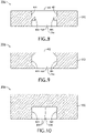
- an inactive face 402 of the two faces 402 may have at least one channel 502 that mechanically interlocks with the mold material 302.
- the IC die 204 may have material removed along the inactive face 402 such that the inactive face 402 of the IC die 204 mechanically interlocks with the mold material 302.
- an inactive face 402 of the two faces 402 may have at least one rough surface that mechanically interlocks with the mold material 302.
- the dicing saw 110 may cut channels 502 into the inactive face 402 of the IC die 204 to increase the surface area that will interface with the mold material 302 so as to allow adhesion of the IC die 204 to the mold material for providing more strongly bonded IC die 204 in the reconstituted wafer 206.
- the channels 502 may be formed by other wafer processing equipment, such as etch equipment 112, 114 that may use a masking material to determine edge and channel 502 geometry.
- At least one of the two faces 402 of the IC die 204 may have a surface area greater than a minimum cross-sectional area extending between the sides 404 such that the IC die 204 mechanically interlocks with the mold material 302.
- the IC die 204 may have material removed along at least one of the sides 404 such that the at least one of the sides 404 of the IC die 204 mechanically interlocks with the mold material 302.
- the wafer processing equipment 108 may remove an amount of the IC die 204 material (e.g., along at least one side 404 and/or at least one face 402) to create a feature that will lock the IC die 204 in place when filled with the mold material 302.
- the IC die 204 material can be removed mechanically, chemically, or by using a reactive ion etching process.
- the wafer processing equipment 108 may remove an amount of the IC die 204 material along at least one side 404 and/or at least one face 402 to create a feature that will mechanically lock the IC die 204 in place when filled with the mold material 302.
- the wafer processing equipment 108 may remove an amount of the IC die 204 material along at least one side 404 and/or at least one face 402 to create a feature that will mechanically lock the IC die 204 in place when filled with the mold material 302.
- the interface between the material removed from the IC die 204 along at least one side 404 and/or at least one face 402 may form a rounded interface between the at least one side 404 and at least one face 402.
- one or more sides 404 may have at least one channel that mechanically interlocks with the mold material 302.
- the reconstituted wafer 206 may be used for dual side processing.
- At least one of the two faces 402 of the IC die 204 may have a surface area less than a maximum cross-sectional area extending between the sides 404 such that the IC die 204 mechanically interlocks with the mold material 302.
- the reconstituted wafer 206 may be used for dual side processing.
- At least one side 404 of the sides 404 may have at least one rough surface that mechanically interlocks with the mold material 302.
- a micro-level interlock that can be imparted to at least one side 404 of the IC die 204 by altering the wafer dicing process.
- traditional dicing procedures aim to reduce the surface roughness of the die edges.
- the roughness on the sides 404 of the IC dies 204 may offer volume for the mold material 302 to occupy acting as many micromechanical interlock features.
- the wafer processing equipment 108 e.g., the dicing saw 110, the grinding and/or polishing wheels 116, and/or etch equipment 112, 114) can form the rough surface.
- intentional scalloping or other micro features can be introduced to the die sides 404 by using the Bosch etch/passivate cyclical process.
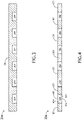
- the reconstituted wafer 206 may include mold material 302, at least one IC die 204 (e.g., a plurality of IC dies 204), at least one redistribution layer 1202, at least one signal pad (e.g., at least one signal ball 1208 and/or at least one signal pin), at least one under bump metallization (UBM) layer 1302, and/or at least one ground pad (e.g., at least one ground ball 1208A and/or at least one ground pin).
- UBM under bump metallization
- Each IC die 204 may have two faces 402 and sides 404.
- the mold material 302 may surround at least the sides 404 of each IC die 204.
- the reconstituted wafer 206 may have backside mold material 302.
- the reconstituted wafer 206 may lack backside mold material 302 such that the two faces 402 of one or more of the at least one IC die 204 are exposed.
- the mold material 302 does not surround either of the two faces 402.
- the redistribution layer 1202 may be positioned between (a) the signal pads and (b) the mold material 302 and each IC die 204.
- the redistribution layer 1202 may have conductive paths 1204 (e.g., at least one stripline transmission line 1304-1, 1304-2) at least connecting an IC die 204 and at least some of the signal pads.
- the redistribution layer 1202 may include at least one ground.
- a surface of the mold material 302 may abut the redistribution layer 1202.
- the surface of the mold material 302 may include at least one recessed area having at least one conductive feature (e.g., at least one conductive path 1206 and/or at least one ground feature (e.g., at least one ground plane 1306)) connected to at least one of the conductive paths 1204 or the IC die 204.
- at least one conductive feature e.g., at least one conductive path 1206 and/or at least one ground feature (e.g., at least one ground plane 1306)
- the ground feature may provide a ground reference for stripline routing of signals in a layer of the redistribution layer 1202 closest to the IC die 204; such signals may be relatively sensitive or relatively high speed signals in the layer of the redistribution layer 1202 closest to the IC die 204, the relatively sensitive or relatively high speed signals being more sensitive or having a higher speed than in a second layer of the redistribution layer 1202, the second layer being farther away from the IC die 204 than the layer.
- the at least one conductive feature of the at least one recessed area may be referred to as at least one zero th layer conductive feature.
- the reconstituted wafer 206 may include a first IC die 204 and a second IC die 204, which may be interconnected by the at least one conductive path 1204 and/or the at least one conductive feature (e.g., the at least one conductive path 1206).
- embedding conductive features into the mold material 302 of reconstituted wafers 206 may provide significant value to microelectronic packaging capabilities. Designs can be miniaturized by incorporating device interconnect, redistribution, and/or grounding into the mold material 302 of the reconstituted wafer 206. Similarly, individual package capability may be enhanced by expanding the design space from the redistribution layer 1202 into the device layer of the reconstituted wafer 206.
- creating a reconstituted wafer 206 having the at least one conductive feature of the at least one recessed area of the mold material 302 may be performed by the wafer processing equipment 108.
- the zero th layer conductive features may be placed or deposited. If the zeroth layer conductive features are to be placed, the zero th layer conductive features (e.g., jumpers, wires, etc.) can be placed in a specified location using pick-and-place equipment 118. If the zeroth layer conductive features are to be deposited, the zero th layer conductive features may be deposited at specified locations, for example, by using a masking material and may be built up via physical and/or chemical vapor deposition, electroplating, aerosol jet dispense systems, etc.
- the zero th layer conductive features may be deposited and/or pick and placed on a non-wetting surface.
- Other zeroth layer components e.g., IC dies 204, resistors, capacitors, etc.
- the zeroth layer conductive features and other zero th layer components may be encapsulated with the mold material 302.
- a redistribution layer 1202 may be built on top of the mold material 302 and zeroth layer features by the wafer processing equipment 108 to connect and/or route zeroth layer conductive features and other zeroth layer components in a desired fashion.
- Typical redistribution layer 1202 buildup often includes, but is not limited to, the following processes: photolithography, vapor deposition, electroplating, and/or aerosol jet printing.
- Typical redistribution layer 1202 buildup often includes, but is not limited to, the following materials: nickel, gold, copper, platinum, and/or permanent photoresist.
- some embodiments may expand the capabilities of microelectronic packaging through a method of embedding printed or deposited conductive features (e.g., conductive paths 1206 (e.g., traces and/or conductive jumpers) and/or ground planes 1306) into the mold material 302 of a reconstituted wafer 206 by the wafer processing equipment 108.
- conductive traces or jumpers may be positioned in a recessed portion of the surface layer of the mold material 302.
- the conductive features can be printed via a controlled dispense process, via thin film deposition, and/or picked and placed using an automated placement process along with the package devices.
- Some embodiments may free up space in the redistribution layer 1202 by integrating some traces and device interconnect into the mold material 302.
- some embodiments include a zeroth layer ground reference for stripline routing of sensitive or high speed signals in a first layer (e.g., closest to the IC die 204) of a standard 2-layer redistribution layer 1202.
- the first layer can be important for break-out routing of dense or sensitive signals, and often cannot be dedicated as a ground plane.
- PCB printed circuit board
- using the zeroth layer as a ground reference not only has the potential to reduce the required layer count by 1 or 2 layers, but can potentially offer the cleanest possible routing for high speed or sensitive radiofrequency (RF) and/or digital signals.
- RF radiofrequency
- the reconstituted wafer 206 may include a possible break-out (e.g., a cleanest possible break-out) by combining stripline configuration with utilizing the UBM layer 1302 for ground to provide minimized via staggering.
- a possible break-out e.g., a cleanest possible break-out
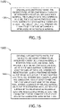
- an exemplary embodiment of a method 1500 may include one or more of the following steps. Additionally, for example, some embodiments may include performing one more instances of the method 1500 iteratively, concurrently, and/or sequentially. Additionally, for example, at least some of the steps of the method 1500 may be performed in parallel and/or concurrently. Additionally, in some embodiments, at least some of the steps of the method 1500 may be performed non-sequentially. Additionally, in some embodiments, at least some of the steps of the method 1500 may be performed in sub-steps of providing various components. In some embodiments, the method 1500 may be performed by the wafer processing equipment 108.
- a step 1502 may include creating a reconstituted wafer, the reconstituted wafer comprising a plurality of integrated circuit (IC) dies and a mold material, the plurality of IC dies comprising an IC die, the IC die having two faces and sides, wherein the mold material surrounds at least the sides of the IC die, wherein the plurality of IC dies are mechanically interlocked with the mold material.
- IC integrated circuit
- method 1500 may include any of the operations disclosed throughout.
- an exemplary embodiment of a method 1600 may include one or more of the following steps. Additionally, for example, some embodiments may include performing one more instances of the method 1600 iteratively, concurrently, and/or sequentially. Additionally, for example, at least some of the steps of the method 1600 may be performed in parallel and/or concurrently. Additionally, in some embodiments, at least some of the steps of the method 1600 may be performed non-sequentially. Additionally, in some embodiments, at least some of the steps of the method 1600 may be performed in sub-steps of providing various components. In some embodiments, the method 1600 may be performed by the wafer processing equipment 108.
- a step 1602 may include creating a reconstituted wafer, the reconstituted wafer comprising an integrated circuit (IC), a mold material, a redistribution layer, and signal pads, wherein the IC die has two faces and sides, wherein the mold material surrounds at least the sides of the IC die, wherein the redistribution layer is positioned between (a) the signal pads and (b) the mold material and the IC die, wherein redistribution layer has conductive paths at least connecting the IC die and at least some of the signal pads, wherein a surface of the mold material abuts the redistribution layer, wherein the surface of the mold material includes at least one recessed area having at least one conductive feature connected to at least one of the conductive paths or the IC die.
- IC integrated circuit
- method 1600 may include any of the operations disclosed throughout.
- embodiments of the inventive concepts disclosed herein may be directed to a method and a system including at least one IC die and mold material.
- At least one non-transitory computer-readable medium may refer to as at least one non-transitory computer-readable medium (e.g., at least one memory device (e.g., a nonvolatile memory device); e.g., at least one memristor; e.g., at least one computer-readable medium implemented as hardware; e.g., at least one non-transitory processor-readable medium, at least one memory (e.g., at least one nonvolatile memory, at least one volatile memory, or a combination thereof; e.g., at least one random-access memory, at least one flash memory, at least one read-only memory (ROM) (e.g., at least one electrically erasable programmable read-only memory (EEPROM)), at least one on-processor memory (e.g., at least one on-processor cache, at least one on-processor buffer, at least one on-processor flash memory, at least one on
- At least one means one or a plurality of; for example, “at least one” may comprise one, two, three, ..., one hundred, or more.
- one or more means one or a plurality of; for example, “one or more” may comprise one, two, three, ..., one hundred, or more.
- zero or more means zero, one, or a plurality of; for example, “zero or more” may comprise zero, one, two, three, ..., one hundred, or more.
- the methods, operations, and/or functionality disclosed may be implemented as sets of instructions or software readable by a device. Further, it is understood that the specific order or hierarchy of steps in the methods, operations, and/or functionality disclosed are examples of exemplary approaches. Based upon design preferences, it is understood that the specific order or hierarchy of steps in the methods, operations, and/or functionality can be rearranged while remaining within the scope of the inventive concepts disclosed herein.
- the accompanying claims may present elements of the various steps in a sample order, and are not necessarily meant to be limited to the specific order or hierarchy presented.
- embodiments of the methods according to the inventive concepts disclosed herein may include one or more of the steps described herein. Further, such steps may be carried out in any desired order and two or more of the steps may be carried out simultaneously with one another. Two or more of the steps disclosed herein may be combined in a single step, and in some embodiments, one or more of the steps may be carried out as two or more sub-steps. Further, other steps or sub-steps may be carried in addition to, or as substitutes to one or more of the steps disclosed herein.
Landscapes
- Internal Circuitry In Semiconductor Integrated Circuit Devices (AREA)
- Physics & Mathematics (AREA)
- Geometry (AREA)
- Engineering & Computer Science (AREA)
- Manufacturing & Machinery (AREA)
- Structures Or Materials For Encapsulating Or Coating Semiconductor Devices Or Solid State Devices (AREA)
Applications Claiming Priority (1)
| Application Number | Priority Date | Filing Date | Title |
|---|---|---|---|
| US17/017,235 US11515225B2 (en) | 2020-09-10 | 2020-09-10 | Reconstituted wafer including mold material with recessed conductive feature |
Publications (2)
| Publication Number | Publication Date |
|---|---|
| EP3979307A2 true EP3979307A2 (de) | 2022-04-06 |
| EP3979307A3 EP3979307A3 (de) | 2022-07-06 |
Family
ID=77738917
Family Applications (1)
| Application Number | Title | Priority Date | Filing Date |
|---|---|---|---|
| EP21195776.6A Pending EP3979307A3 (de) | 2020-09-10 | 2021-09-09 | Rekonstituierter wafer mit formmaterial mit vertieftem leitendem merkmal |
Country Status (2)
| Country | Link |
|---|---|
| US (1) | US11515225B2 (de) |
| EP (1) | EP3979307A3 (de) |
Family Cites Families (33)
| Publication number | Priority date | Publication date | Assignee | Title |
|---|---|---|---|---|
| US7208345B2 (en) | 2005-05-11 | 2007-04-24 | Infineon Technologies Ag | Method of manufacturing a semiconductor device comprising stacked chips and a corresponding semiconductor device |
| US7300824B2 (en) | 2005-08-18 | 2007-11-27 | James Sheats | Method of packaging and interconnection of integrated circuits |
| FR2946795B1 (fr) | 2009-06-12 | 2011-07-22 | 3D Plus | Procede de positionnement des puces lors de la fabrication d'une plaque reconstituee |
| US20110215465A1 (en) | 2010-03-03 | 2011-09-08 | Xilinx, Inc. | Multi-chip integrated circuit |
| US8535989B2 (en) | 2010-04-02 | 2013-09-17 | Intel Corporation | Embedded semiconductive chips in reconstituted wafers, and systems containing same |
| US10204879B2 (en) | 2011-01-21 | 2019-02-12 | STATS ChipPAC Pte. Ltd. | Semiconductor device and method of forming wafer-level interconnect structures with advanced dielectric characteristics |
| US20120282767A1 (en) | 2011-05-05 | 2012-11-08 | Stmicroelectronics Pte Ltd. | Method for producing a two-sided fan-out wafer level package with electrically conductive interconnects, and a corresponding semiconductor package |
| US8916481B2 (en) | 2011-11-02 | 2014-12-23 | Stmicroelectronics Pte Ltd. | Embedded wafer level package for 3D and package-on-package applications, and method of manufacture |
| US8922013B2 (en) | 2011-11-08 | 2014-12-30 | Stmicroelectronics Pte Ltd. | Through via package |
| US20130154106A1 (en) | 2011-12-14 | 2013-06-20 | Broadcom Corporation | Stacked Packaging Using Reconstituted Wafers |
| US9058455B2 (en) | 2012-01-20 | 2015-06-16 | International Business Machines Corporation | Backside integration of RF filters for RF front end modules and design structure |
| US11213690B2 (en) | 2012-06-15 | 2022-01-04 | Medtronic, Inc. | Wafer level packages of high voltage units for implantable medical devices |
| US20140057394A1 (en) | 2012-08-24 | 2014-02-27 | Stmicroelectronics Pte Ltd. | Method for making a double-sided fanout semiconductor package with embedded surface mount devices, and product made |
| US9620413B2 (en) | 2012-10-02 | 2017-04-11 | STATS ChipPAC Pte. Ltd. | Semiconductor device and method of using a standardized carrier in semiconductor packaging |
| US9177884B2 (en) | 2012-10-09 | 2015-11-03 | Avago Technologies General Ip (Singapore) Pte. Ltd. | Two-sided-access extended wafer-level ball grid array (eWLB) package, assembly and method |
| US9257355B2 (en) | 2013-02-11 | 2016-02-09 | The Charles Stark Draper Laboratory, Inc. | Method for embedding a chipset having an intermediary interposer in high density electronic modules |
| JP2014192170A (ja) | 2013-03-26 | 2014-10-06 | Fujitsu Ltd | 半導体装置の製造方法および半導体装置 |
| US9390993B2 (en) | 2014-08-15 | 2016-07-12 | Broadcom Corporation | Semiconductor border protection sealant |
| US11069734B2 (en) | 2014-12-11 | 2021-07-20 | Invensas Corporation | Image sensor device |
| US9633974B2 (en) * | 2015-03-04 | 2017-04-25 | Apple Inc. | System in package fan out stacking architecture and process flow |
| US9806040B2 (en) * | 2015-07-29 | 2017-10-31 | STATS ChipPAC Pte. Ltd. | Antenna in embedded wafer-level ball-grid array package |
| KR101743467B1 (ko) | 2015-08-24 | 2017-06-07 | 주식회사 에스에프에이반도체 | 팬-아웃형 웨이퍼 레벨 패키지의 제조 방법 |
| KR102384863B1 (ko) * | 2015-09-09 | 2022-04-08 | 삼성전자주식회사 | 반도체 칩 패키지 및 이의 제조 방법 |
| US10186468B2 (en) * | 2016-03-31 | 2019-01-22 | Infineon Technologies Ag | System and method for a transducer in an eWLB package |
| TWI624894B (zh) | 2016-08-12 | 2018-05-21 | 鴻騏新技股份有限公司 | 重組式晶圓的對貼方法 |
| US10515927B2 (en) | 2017-04-21 | 2019-12-24 | Applied Materials, Inc. | Methods and apparatus for semiconductor package processing |
| US10217720B2 (en) | 2017-06-15 | 2019-02-26 | Invensas Corporation | Multi-chip modules formed using wafer-level processing of a reconstitute wafer |
| US10347574B2 (en) * | 2017-09-28 | 2019-07-09 | Taiwan Semiconductor Manufacturing Co., Ltd. | Integrated fan-out packages |
| US20190165108A1 (en) | 2017-11-30 | 2019-05-30 | Raytheon Company | Reconstituted wafer structure |
| WO2019222525A1 (en) | 2018-05-17 | 2019-11-21 | Gulfstream Aerospace Corporation | Tactile responsive surface for virtual reality training device |
| KR102554690B1 (ko) * | 2018-11-06 | 2023-07-13 | 삼성전자주식회사 | 반도체 패키지 |
| US20200161206A1 (en) | 2018-11-20 | 2020-05-21 | Advanced Semiconductor Engineering, Inc. | Semiconductor package structure and semiconductor manufacturing process |
| US11532867B2 (en) | 2018-12-28 | 2022-12-20 | Taiwan Semiconductor Manufacturing Company, Ltd. | Heterogeneous antenna in fan-out package |
-
2020
- 2020-09-10 US US17/017,235 patent/US11515225B2/en active Active
-
2021
- 2021-09-09 EP EP21195776.6A patent/EP3979307A3/de active Pending
Also Published As
| Publication number | Publication date |
|---|---|
| US20220077015A1 (en) | 2022-03-10 |
| US11515225B2 (en) | 2022-11-29 |
| EP3979307A3 (de) | 2022-07-06 |
Similar Documents
| Publication | Publication Date | Title |
|---|---|---|
| US10734370B2 (en) | Methods of making semiconductor devices | |
| US9396999B2 (en) | Wafer level packaging method | |
| US8604600B2 (en) | Fully molded fan-out | |
| US8455301B2 (en) | Method of fabricating stacked chips in a semiconductor package | |
| CN107548519B (zh) | 用于半导体器件的具有高高宽比的穿过电介质的导电路径 | |
| US11652057B2 (en) | Disaggregated die interconnection with on-silicon cavity bridge | |
| CN107527895B (zh) | 集体制造配置成在高于1GHz下工作的3D电子组件的方法 | |
| US11309279B2 (en) | Package structure of wafer-level system-in-package | |
| CN104037134B (zh) | 电子元件的扇出和异构性封装 | |
| TW201618176A (zh) | 晶片封裝體及其製造方法 | |
| CN103848391B (zh) | 嵌入式芯片封装、芯片封装和制备嵌入式芯片封装的方法 | |
| CN106298558A (zh) | 包括插入物的半导体封装及其制造方法 | |
| US10770432B2 (en) | ASICS face to face self assembly | |
| US20260107807A1 (en) | Wafer level packaging having redistribution layer formed utilizing laser direct structuring | |
| EP3214643A2 (de) | Umspritztes gehäuse in chipgrösse | |
| WO2017091276A1 (en) | Provision of structural integrity in memory device | |
| US11515225B2 (en) | Reconstituted wafer including mold material with recessed conductive feature | |
| US11605570B2 (en) | Reconstituted wafer including integrated circuit die mechanically interlocked with mold material | |
| EP3367430B1 (de) | Verfahren zur herstellung eines halbleiterbauelementes mit sechsseitig geschützten wänden | |
| JP4673167B2 (ja) | 半導体装置およびその製造方法 | |
| CN113539984A (zh) | 半导体结构及其形成方法 |
Legal Events
| Date | Code | Title | Description |
|---|---|---|---|
| PUAI | Public reference made under article 153(3) epc to a published international application that has entered the european phase |
Free format text: ORIGINAL CODE: 0009012 |
|
| STAA | Information on the status of an ep patent application or granted ep patent |
Free format text: STATUS: THE APPLICATION HAS BEEN PUBLISHED |
|
| AK | Designated contracting states |
Kind code of ref document: A2 Designated state(s): AL AT BE BG CH CY CZ DE DK EE ES FI FR GB GR HR HU IE IS IT LI LT LU LV MC MK MT NL NO PL PT RO RS SE SI SK SM TR |
|
| PUAL | Search report despatched |
Free format text: ORIGINAL CODE: 0009013 |
|
| AK | Designated contracting states |
Kind code of ref document: A3 Designated state(s): AL AT BE BG CH CY CZ DE DK EE ES FI FR GB GR HR HU IE IS IT LI LT LU LV MC MK MT NL NO PL PT RO RS SE SI SK SM TR |
|
| RIC1 | Information provided on ipc code assigned before grant |
Ipc: H01L 23/66 20060101ALI20220601BHEP Ipc: H01L 23/00 20060101AFI20220601BHEP |
|
| STAA | Information on the status of an ep patent application or granted ep patent |
Free format text: STATUS: REQUEST FOR EXAMINATION WAS MADE |
|
| 17P | Request for examination filed |
Effective date: 20230103 |
|
| RBV | Designated contracting states (corrected) |
Designated state(s): AL AT BE BG CH CY CZ DE DK EE ES FI FR GB GR HR HU IE IS IT LI LT LU LV MC MK MT NL NO PL PT RO RS SE SI SK SM TR |