EP3978495B1 - Organic electroluminescence device and polycyclic compound for organic electroluminescence device - Google Patents
Organic electroluminescence device and polycyclic compound for organic electroluminescence device Download PDFInfo
- Publication number
- EP3978495B1 EP3978495B1 EP21203301.3A EP21203301A EP3978495B1 EP 3978495 B1 EP3978495 B1 EP 3978495B1 EP 21203301 A EP21203301 A EP 21203301A EP 3978495 B1 EP3978495 B1 EP 3978495B1
- Authority
- EP
- European Patent Office
- Prior art keywords
- layer
- substituted
- organic electroluminescence
- group
- electrode
- Prior art date
- Legal status (The legal status is an assumption and is not a legal conclusion. Google has not performed a legal analysis and makes no representation as to the accuracy of the status listed.)
- Active
Links
- -1 polycyclic compound Chemical class 0.000 title claims description 113
- 238000005401 electroluminescence Methods 0.000 title claims description 42
- 150000001875 compounds Chemical class 0.000 claims description 63
- 230000005525 hole transport Effects 0.000 claims description 49
- 238000002347 injection Methods 0.000 claims description 35
- 239000007924 injection Substances 0.000 claims description 35
- 125000004432 carbon atom Chemical group C* 0.000 claims description 32
- 125000003118 aryl group Chemical group 0.000 claims description 24
- 239000002019 doping agent Substances 0.000 claims description 23
- 230000000903 blocking effect Effects 0.000 claims description 18
- 125000000217 alkyl group Chemical group 0.000 claims description 17
- 125000001072 heteroaryl group Chemical group 0.000 claims description 15
- 125000004435 hydrogen atom Chemical group [H]* 0.000 claims description 15
- 230000003111 delayed effect Effects 0.000 claims description 11
- 229910052805 deuterium Inorganic materials 0.000 claims description 10
- 125000004431 deuterium atom Chemical group 0.000 claims description 10
- 229910052757 nitrogen Inorganic materials 0.000 claims description 10
- 125000001997 phenyl group Chemical group [H]C1=C([H])C([H])=C(*)C([H])=C1[H] 0.000 claims description 9
- 229910052799 carbon Inorganic materials 0.000 claims description 6
- 229910052710 silicon Inorganic materials 0.000 claims description 4
- 239000010410 layer Substances 0.000 description 147
- 230000000052 comparative effect Effects 0.000 description 44
- 239000000463 material Substances 0.000 description 38
- 238000000034 method Methods 0.000 description 22
- YXFVVABEGXRONW-UHFFFAOYSA-N Toluene Chemical compound CC1=CC=CC=C1 YXFVVABEGXRONW-UHFFFAOYSA-N 0.000 description 15
- 239000002356 single layer Substances 0.000 description 12
- HUWSZNZAROKDRZ-RRLWZMAJSA-N (3r,4r)-3-azaniumyl-5-[[(2s,3r)-1-[(2s)-2,3-dicarboxypyrrolidin-1-yl]-3-methyl-1-oxopentan-2-yl]amino]-5-oxo-4-sulfanylpentane-1-sulfonate Chemical compound OS(=O)(=O)CC[C@@H](N)[C@@H](S)C(=O)N[C@@H]([C@H](C)CC)C(=O)N1CCC(C(O)=O)[C@H]1C(O)=O HUWSZNZAROKDRZ-RRLWZMAJSA-N 0.000 description 9
- 125000001424 substituent group Chemical group 0.000 description 9
- 230000015572 biosynthetic process Effects 0.000 description 8
- 125000000623 heterocyclic group Chemical group 0.000 description 8
- 238000003786 synthesis reaction Methods 0.000 description 8
- XLOMVQKBTHCTTD-UHFFFAOYSA-N Zinc monoxide Chemical compound [Zn]=O XLOMVQKBTHCTTD-UHFFFAOYSA-N 0.000 description 7
- 239000000872 buffer Substances 0.000 description 7
- 238000004992 fast atom bombardment mass spectroscopy Methods 0.000 description 7
- 229910052751 metal Inorganic materials 0.000 description 7
- 239000002184 metal Substances 0.000 description 7
- 239000000203 mixture Substances 0.000 description 7
- OOKAZRDERJMRCJ-KOUAFAAESA-N (3r)-7-[(1s,2s,4ar,6s,8s)-2,6-dimethyl-8-[(2s)-2-methylbutanoyl]oxy-1,2,4a,5,6,7,8,8a-octahydronaphthalen-1-yl]-3-hydroxy-5-oxoheptanoic acid Chemical compound C1=C[C@H](C)[C@H](CCC(=O)C[C@@H](O)CC(O)=O)C2[C@@H](OC(=O)[C@@H](C)CC)C[C@@H](C)C[C@@H]21 OOKAZRDERJMRCJ-KOUAFAAESA-N 0.000 description 6
- ATTVYRDSOVWELU-UHFFFAOYSA-N 1-diphenylphosphoryl-2-(2-diphenylphosphorylphenoxy)benzene Chemical compound C=1C=CC=CC=1P(C=1C(=CC=CC=1)OC=1C(=CC=CC=1)P(=O)(C=1C=CC=CC=1)C=1C=CC=CC=1)(=O)C1=CC=CC=C1 ATTVYRDSOVWELU-UHFFFAOYSA-N 0.000 description 6
- GSDQYSSLIKJJOG-UHFFFAOYSA-N 4-chloro-2-(3-chloroanilino)benzoic acid Chemical compound OC(=O)C1=CC=C(Cl)C=C1NC1=CC=CC(Cl)=C1 GSDQYSSLIKJJOG-UHFFFAOYSA-N 0.000 description 6
- XKRFYHLGVUSROY-UHFFFAOYSA-N Argon Chemical compound [Ar] XKRFYHLGVUSROY-UHFFFAOYSA-N 0.000 description 6
- ZOXJGFHDIHLPTG-UHFFFAOYSA-N Boron Chemical group [B] ZOXJGFHDIHLPTG-UHFFFAOYSA-N 0.000 description 6
- 229920000767 polyaniline Polymers 0.000 description 6
- AWXGSYPUMWKTBR-UHFFFAOYSA-N 4-carbazol-9-yl-n,n-bis(4-carbazol-9-ylphenyl)aniline Chemical compound C12=CC=CC=C2C2=CC=CC=C2N1C1=CC=C(N(C=2C=CC(=CC=2)N2C3=CC=CC=C3C3=CC=CC=C32)C=2C=CC(=CC=2)N2C3=CC=CC=C3C3=CC=CC=C32)C=C1 AWXGSYPUMWKTBR-UHFFFAOYSA-N 0.000 description 5
- 229910052782 aluminium Inorganic materials 0.000 description 5
- 239000011575 calcium Substances 0.000 description 5
- 239000011777 magnesium Substances 0.000 description 5
- VFUDMQLBKNMONU-UHFFFAOYSA-N 9-[4-(4-carbazol-9-ylphenyl)phenyl]carbazole Chemical group C12=CC=CC=C2C2=CC=CC=C2N1C1=CC=C(C=2C=CC(=CC=2)N2C3=CC=CC=C3C3=CC=CC=C32)C=C1 VFUDMQLBKNMONU-UHFFFAOYSA-N 0.000 description 4
- OKTJSMMVPCPJKN-UHFFFAOYSA-N Carbon Chemical group [C] OKTJSMMVPCPJKN-UHFFFAOYSA-N 0.000 description 4
- PXHVJJICTQNCMI-UHFFFAOYSA-N Nickel Chemical compound [Ni] PXHVJJICTQNCMI-UHFFFAOYSA-N 0.000 description 4
- KDLHZDBZIXYQEI-UHFFFAOYSA-N Palladium Chemical compound [Pd] KDLHZDBZIXYQEI-UHFFFAOYSA-N 0.000 description 4
- 239000007983 Tris buffer Substances 0.000 description 4
- 125000003277 amino group Chemical group 0.000 description 4
- 238000006243 chemical reaction Methods 0.000 description 4
- 125000003983 fluorenyl group Chemical group C1(=CC=CC=2C3=CC=CC=C3CC12)* 0.000 description 4
- 229910052749 magnesium Inorganic materials 0.000 description 4
- 229910044991 metal oxide Inorganic materials 0.000 description 4
- 150000004706 metal oxides Chemical class 0.000 description 4
- BASFCYQUMIYNBI-UHFFFAOYSA-N platinum Chemical compound [Pt] BASFCYQUMIYNBI-UHFFFAOYSA-N 0.000 description 4
- LVTJOONKWUXEFR-FZRMHRINSA-N protoneodioscin Natural products O(C[C@@H](CC[C@]1(O)[C@H](C)[C@@H]2[C@]3(C)[C@H]([C@H]4[C@@H]([C@]5(C)C(=CC4)C[C@@H](O[C@@H]4[C@H](O[C@H]6[C@@H](O)[C@@H](O)[C@@H](O)[C@H](C)O6)[C@@H](O)[C@H](O[C@H]6[C@@H](O)[C@@H](O)[C@@H](O)[C@H](C)O6)[C@H](CO)O4)CC5)CC3)C[C@@H]2O1)C)[C@H]1[C@H](O)[C@H](O)[C@H](O)[C@@H](CO)O1 LVTJOONKWUXEFR-FZRMHRINSA-N 0.000 description 4
- 229910052709 silver Inorganic materials 0.000 description 4
- 238000003756 stirring Methods 0.000 description 4
- 238000010189 synthetic method Methods 0.000 description 4
- GEQBRULPNIVQPP-UHFFFAOYSA-N 2-[3,5-bis(1-phenylbenzimidazol-2-yl)phenyl]-1-phenylbenzimidazole Chemical compound C1=CC=CC=C1N1C2=CC=CC=C2N=C1C1=CC(C=2N(C3=CC=CC=C3N=2)C=2C=CC=CC=2)=CC(C=2N(C3=CC=CC=C3N=2)C=2C=CC=CC=2)=C1 GEQBRULPNIVQPP-UHFFFAOYSA-N 0.000 description 3
- RAPHUPWIHDYTKU-WXUKJITCSA-N 9-ethyl-3-[(e)-2-[4-[4-[(e)-2-(9-ethylcarbazol-3-yl)ethenyl]phenyl]phenyl]ethenyl]carbazole Chemical group C1=CC=C2C3=CC(/C=C/C4=CC=C(C=C4)C4=CC=C(C=C4)/C=C/C=4C=C5C6=CC=CC=C6N(C5=CC=4)CC)=CC=C3N(CC)C2=C1 RAPHUPWIHDYTKU-WXUKJITCSA-N 0.000 description 3
- 101000837344 Homo sapiens T-cell leukemia translocation-altered gene protein Proteins 0.000 description 3
- 102100028692 T-cell leukemia translocation-altered gene protein Human genes 0.000 description 3
- 125000003342 alkenyl group Chemical group 0.000 description 3
- XAGFODPZIPBFFR-UHFFFAOYSA-N aluminium Chemical compound [Al] XAGFODPZIPBFFR-UHFFFAOYSA-N 0.000 description 3
- 229910052786 argon Inorganic materials 0.000 description 3
- 239000011651 chromium Substances 0.000 description 3
- 239000010949 copper Substances 0.000 description 3
- 239000012043 crude product Substances 0.000 description 3
- 125000004093 cyano group Chemical group *C#N 0.000 description 3
- 238000004821 distillation Methods 0.000 description 3
- 239000010931 gold Substances 0.000 description 3
- 125000005843 halogen group Chemical group 0.000 description 3
- 125000005842 heteroatom Chemical group 0.000 description 3
- RAXXELZNTBOGNW-UHFFFAOYSA-N imidazole Natural products C1=CNC=N1 RAXXELZNTBOGNW-UHFFFAOYSA-N 0.000 description 3
- VLKZOEOYAKHREP-UHFFFAOYSA-N n-Hexane Chemical compound CCCCCC VLKZOEOYAKHREP-UHFFFAOYSA-N 0.000 description 3
- 239000012044 organic layer Substances 0.000 description 3
- 125000002524 organometallic group Chemical group 0.000 description 3
- MPQXHAGKBWFSNV-UHFFFAOYSA-N oxidophosphanium Chemical group [PH3]=O MPQXHAGKBWFSNV-UHFFFAOYSA-N 0.000 description 3
- 229920003227 poly(N-vinyl carbazole) Polymers 0.000 description 3
- XSCHRSMBECNVNS-UHFFFAOYSA-N quinoxaline Chemical compound N1=CC=NC2=CC=CC=C21 XSCHRSMBECNVNS-UHFFFAOYSA-N 0.000 description 3
- 238000010898 silica gel chromatography Methods 0.000 description 3
- 125000003808 silyl group Chemical group [H][Si]([H])([H])[*] 0.000 description 3
- 239000007787 solid Substances 0.000 description 3
- 239000002904 solvent Substances 0.000 description 3
- 239000010936 titanium Substances 0.000 description 3
- ODHXBMXNKOYIBV-UHFFFAOYSA-N triphenylamine Chemical compound C1=CC=CC=C1N(C=1C=CC=CC=1)C1=CC=CC=C1 ODHXBMXNKOYIBV-UHFFFAOYSA-N 0.000 description 3
- 238000001771 vacuum deposition Methods 0.000 description 3
- XLYOFNOQVPJJNP-UHFFFAOYSA-N water Substances O XLYOFNOQVPJJNP-UHFFFAOYSA-N 0.000 description 3
- 239000011787 zinc oxide Substances 0.000 description 3
- CYPYTURSJDMMMP-WVCUSYJESA-N (1e,4e)-1,5-diphenylpenta-1,4-dien-3-one;palladium Chemical compound [Pd].[Pd].C=1C=CC=CC=1\C=C\C(=O)\C=C\C1=CC=CC=C1.C=1C=CC=CC=1\C=C\C(=O)\C=C\C1=CC=CC=C1.C=1C=CC=CC=1\C=C\C(=O)\C=C\C1=CC=CC=C1 CYPYTURSJDMMMP-WVCUSYJESA-N 0.000 description 2
- YJTKZCDBKVTVBY-UHFFFAOYSA-N 1,3-Diphenylbenzene Chemical group C1=CC=CC=C1C1=CC=CC(C=2C=CC=CC=2)=C1 YJTKZCDBKVTVBY-UHFFFAOYSA-N 0.000 description 2
- FCEHBMOGCRZNNI-UHFFFAOYSA-N 1-benzothiophene Chemical compound C1=CC=C2SC=CC2=C1 FCEHBMOGCRZNNI-UHFFFAOYSA-N 0.000 description 2
- IYZMXHQDXZKNCY-UHFFFAOYSA-N 1-n,1-n-diphenyl-4-n,4-n-bis[4-(n-phenylanilino)phenyl]benzene-1,4-diamine Chemical compound C1=CC=CC=C1N(C=1C=CC(=CC=1)N(C=1C=CC(=CC=1)N(C=1C=CC=CC=1)C=1C=CC=CC=1)C=1C=CC(=CC=1)N(C=1C=CC=CC=1)C=1C=CC=CC=1)C1=CC=CC=C1 IYZMXHQDXZKNCY-UHFFFAOYSA-N 0.000 description 2
- PRWATGACIORDEL-UHFFFAOYSA-N 2,4,5,6-tetra(carbazol-9-yl)benzene-1,3-dicarbonitrile Chemical compound C12=CC=CC=C2C2=CC=CC=C2N1C1=C(C#N)C(N2C3=CC=CC=C3C3=CC=CC=C32)=C(N2C3=CC=CC=C3C3=CC=CC=C32)C(N2C3=CC=CC=C3C3=CC=CC=C32)=C1C#N PRWATGACIORDEL-UHFFFAOYSA-N 0.000 description 2
- AIAJGVRFXREWPK-UHFFFAOYSA-N 2,8-bis(diphenylphosphoryl)dibenzofuran Chemical compound C=1C=CC=CC=1P(C=1C=C2C3=CC(=CC=C3OC2=CC=1)P(=O)(C=1C=CC=CC=1)C=1C=CC=CC=1)(=O)C1=CC=CC=C1 AIAJGVRFXREWPK-UHFFFAOYSA-N 0.000 description 2
- STTGYIUESPWXOW-UHFFFAOYSA-N 2,9-dimethyl-4,7-diphenyl-1,10-phenanthroline Chemical compound C=12C=CC3=C(C=4C=CC=CC=4)C=C(C)N=C3C2=NC(C)=CC=1C1=CC=CC=C1 STTGYIUESPWXOW-UHFFFAOYSA-N 0.000 description 2
- IXHWGNYCZPISET-UHFFFAOYSA-N 2-[4-(dicyanomethylidene)-2,3,5,6-tetrafluorocyclohexa-2,5-dien-1-ylidene]propanedinitrile Chemical compound FC1=C(F)C(=C(C#N)C#N)C(F)=C(F)C1=C(C#N)C#N IXHWGNYCZPISET-UHFFFAOYSA-N 0.000 description 2
- HNWFFTUWRIGBNM-UHFFFAOYSA-N 2-methyl-9,10-dinaphthalen-2-ylanthracene Chemical compound C1=CC=CC2=CC(C3=C4C=CC=CC4=C(C=4C=C5C=CC=CC5=CC=4)C4=CC=C(C=C43)C)=CC=C21 HNWFFTUWRIGBNM-UHFFFAOYSA-N 0.000 description 2
- OBAJPWYDYFEBTF-UHFFFAOYSA-N 2-tert-butyl-9,10-dinaphthalen-2-ylanthracene Chemical compound C1=CC=CC2=CC(C3=C4C=CC=CC4=C(C=4C=C5C=CC=CC5=CC=4)C4=CC=C(C=C43)C(C)(C)C)=CC=C21 OBAJPWYDYFEBTF-UHFFFAOYSA-N 0.000 description 2
- QMXFUIUEGUOSEV-UHFFFAOYSA-N 3,4,5,6-tetra(carbazol-9-yl)benzene-1,2-dicarbonitrile Chemical compound N#Cc1c(C#N)c(c(c(c1-n1c2ccccc2c2ccccc12)-n1c2ccccc2c2ccccc12)-n1c2ccccc2c2ccccc12)-n1c2ccccc2c2ccccc12 QMXFUIUEGUOSEV-UHFFFAOYSA-N 0.000 description 2
- ZVFQEOPUXVPSLB-UHFFFAOYSA-N 3-(4-tert-butylphenyl)-4-phenyl-5-(4-phenylphenyl)-1,2,4-triazole Chemical compound C1=CC(C(C)(C)C)=CC=C1C(N1C=2C=CC=CC=2)=NN=C1C1=CC=C(C=2C=CC=CC=2)C=C1 ZVFQEOPUXVPSLB-UHFFFAOYSA-N 0.000 description 2
- DHDHJYNTEFLIHY-UHFFFAOYSA-N 4,7-diphenyl-1,10-phenanthroline Chemical compound C1=CC=CC=C1C1=CC=NC2=C1C=CC1=C(C=3C=CC=CC=3)C=CN=C21 DHDHJYNTEFLIHY-UHFFFAOYSA-N 0.000 description 2
- ZOKIJILZFXPFTO-UHFFFAOYSA-N 4-methyl-n-[4-[1-[4-(4-methyl-n-(4-methylphenyl)anilino)phenyl]cyclohexyl]phenyl]-n-(4-methylphenyl)aniline Chemical compound C1=CC(C)=CC=C1N(C=1C=CC(=CC=1)C1(CCCCC1)C=1C=CC(=CC=1)N(C=1C=CC(C)=CC=1)C=1C=CC(C)=CC=1)C1=CC=C(C)C=C1 ZOKIJILZFXPFTO-UHFFFAOYSA-N 0.000 description 2
- AOQKGYRILLEVJV-UHFFFAOYSA-N 4-naphthalen-1-yl-3,5-diphenyl-1,2,4-triazole Chemical compound C1=CC=CC=C1C(N1C=2C3=CC=CC=C3C=CC=2)=NN=C1C1=CC=CC=C1 AOQKGYRILLEVJV-UHFFFAOYSA-N 0.000 description 2
- VIZUPBYFLORCRA-UHFFFAOYSA-N 9,10-dinaphthalen-2-ylanthracene Chemical compound C12=CC=CC=C2C(C2=CC3=CC=CC=C3C=C2)=C(C=CC=C2)C2=C1C1=CC=C(C=CC=C2)C2=C1 VIZUPBYFLORCRA-UHFFFAOYSA-N 0.000 description 2
- MZYDBGLUVPLRKR-UHFFFAOYSA-N 9-(3-carbazol-9-ylphenyl)carbazole Chemical compound C12=CC=CC=C2C2=CC=CC=C2N1C1=CC(N2C3=CC=CC=C3C3=CC=CC=C32)=CC=C1 MZYDBGLUVPLRKR-UHFFFAOYSA-N 0.000 description 2
- LTUJKAYZIMMJEP-UHFFFAOYSA-N 9-[4-(4-carbazol-9-yl-2-methylphenyl)-3-methylphenyl]carbazole Chemical group C12=CC=CC=C2C2=CC=CC=C2N1C1=CC=C(C=2C(=CC(=CC=2)N2C3=CC=CC=C3C3=CC=CC=C32)C)C(C)=C1 LTUJKAYZIMMJEP-UHFFFAOYSA-N 0.000 description 2
- UJOBWOGCFQCDNV-UHFFFAOYSA-N 9H-carbazole Chemical compound C1=CC=C2C3=CC=CC=C3NC2=C1 UJOBWOGCFQCDNV-UHFFFAOYSA-N 0.000 description 2
- RTZKZFJDLAIYFH-UHFFFAOYSA-N Diethyl ether Chemical class CCOCC RTZKZFJDLAIYFH-UHFFFAOYSA-N 0.000 description 2
- YLQBMQCUIZJEEH-UHFFFAOYSA-N Furan Chemical compound C=1C=COC=1 YLQBMQCUIZJEEH-UHFFFAOYSA-N 0.000 description 2
- SIKJAQJRHWYJAI-UHFFFAOYSA-N Indole Chemical compound C1=CC=C2NC=CC2=C1 SIKJAQJRHWYJAI-UHFFFAOYSA-N 0.000 description 2
- 229910052779 Neodymium Inorganic materials 0.000 description 2
- 229920001609 Poly(3,4-ethylenedioxythiophene) Polymers 0.000 description 2
- JUJWROOIHBZHMG-UHFFFAOYSA-N Pyridine Chemical compound C1=CC=NC=C1 JUJWROOIHBZHMG-UHFFFAOYSA-N 0.000 description 2
- KAESVJOAVNADME-UHFFFAOYSA-N Pyrrole Chemical compound C=1C=CNC=1 KAESVJOAVNADME-UHFFFAOYSA-N 0.000 description 2
- SMWDFEZZVXVKRB-UHFFFAOYSA-N Quinoline Chemical compound N1=CC=CC2=CC=CC=C21 SMWDFEZZVXVKRB-UHFFFAOYSA-N 0.000 description 2
- XUIMIQQOPSSXEZ-UHFFFAOYSA-N Silicon Chemical compound [Si] XUIMIQQOPSSXEZ-UHFFFAOYSA-N 0.000 description 2
- FAPWRFPIFSIZLT-UHFFFAOYSA-M Sodium chloride Chemical compound [Na+].[Cl-] FAPWRFPIFSIZLT-UHFFFAOYSA-M 0.000 description 2
- FZWLAAWBMGSTSO-UHFFFAOYSA-N Thiazole Chemical compound C1=CSC=N1 FZWLAAWBMGSTSO-UHFFFAOYSA-N 0.000 description 2
- YTPLMLYBLZKORZ-UHFFFAOYSA-N Thiophene Chemical compound C=1C=CSC=1 YTPLMLYBLZKORZ-UHFFFAOYSA-N 0.000 description 2
- DZBUGLKDJFMEHC-UHFFFAOYSA-N acridine Chemical compound C1=CC=CC2=CC3=CC=CC=C3N=C21 DZBUGLKDJFMEHC-UHFFFAOYSA-N 0.000 description 2
- 150000001336 alkenes Chemical class 0.000 description 2
- 125000002490 anilino group Chemical group [H]N(*)C1=C([H])C([H])=C([H])C([H])=C1[H] 0.000 description 2
- MWPLVEDNUUSJAV-UHFFFAOYSA-N anthracene Chemical compound C1=CC=CC2=CC3=CC=CC=C3C=C21 MWPLVEDNUUSJAV-UHFFFAOYSA-N 0.000 description 2
- 125000002178 anthracenyl group Chemical group C1(=CC=CC2=CC3=CC=CC=C3C=C12)* 0.000 description 2
- IOJUPLGTWVMSFF-UHFFFAOYSA-N benzothiazole Chemical compound C1=CC=C2SC=NC2=C1 IOJUPLGTWVMSFF-UHFFFAOYSA-N 0.000 description 2
- 125000006267 biphenyl group Chemical group 0.000 description 2
- UFVXQDWNSAGPHN-UHFFFAOYSA-K bis[(2-methylquinolin-8-yl)oxy]-(4-phenylphenoxy)alumane Chemical compound [Al+3].C1=CC=C([O-])C2=NC(C)=CC=C21.C1=CC=C([O-])C2=NC(C)=CC=C21.C1=CC([O-])=CC=C1C1=CC=CC=C1 UFVXQDWNSAGPHN-UHFFFAOYSA-K 0.000 description 2
- 229910052791 calcium Inorganic materials 0.000 description 2
- 229910052804 chromium Inorganic materials 0.000 description 2
- 229910052802 copper Inorganic materials 0.000 description 2
- TXCDCPKCNAJMEE-UHFFFAOYSA-N dibenzofuran Chemical compound C1=CC=C2C3=CC=CC=C3OC2=C1 TXCDCPKCNAJMEE-UHFFFAOYSA-N 0.000 description 2
- IYYZUPMFVPLQIF-UHFFFAOYSA-N dibenzothiophene Chemical compound C1=CC=C2C3=CC=CC=C3SC2=C1 IYYZUPMFVPLQIF-UHFFFAOYSA-N 0.000 description 2
- ZUOUZKKEUPVFJK-UHFFFAOYSA-N diphenyl Chemical compound C1=CC=CC=C1C1=CC=CC=C1 ZUOUZKKEUPVFJK-UHFFFAOYSA-N 0.000 description 2
- DKHNGUNXLDCATP-UHFFFAOYSA-N dipyrazino[2,3-f:2',3'-h]quinoxaline-2,3,6,7,10,11-hexacarbonitrile Chemical compound C12=NC(C#N)=C(C#N)N=C2C2=NC(C#N)=C(C#N)N=C2C2=C1N=C(C#N)C(C#N)=N2 DKHNGUNXLDCATP-UHFFFAOYSA-N 0.000 description 2
- NIHNNTQXNPWCJQ-UHFFFAOYSA-N fluorene Chemical compound C1=CC=C2CC3=CC=CC=C3C2=C1 NIHNNTQXNPWCJQ-UHFFFAOYSA-N 0.000 description 2
- 229910052737 gold Inorganic materials 0.000 description 2
- 230000005283 ground state Effects 0.000 description 2
- 238000010438 heat treatment Methods 0.000 description 2
- 238000007641 inkjet printing Methods 0.000 description 2
- 229910052741 iridium Inorganic materials 0.000 description 2
- AWJUIBRHMBBTKR-UHFFFAOYSA-N isoquinoline Chemical compound C1=NC=CC2=CC=CC=C21 AWJUIBRHMBBTKR-UHFFFAOYSA-N 0.000 description 2
- 238000007648 laser printing Methods 0.000 description 2
- 229910052744 lithium Inorganic materials 0.000 description 2
- IMKMFBIYHXBKRX-UHFFFAOYSA-M lithium;quinoline-2-carboxylate Chemical compound [Li+].C1=CC=CC2=NC(C(=O)[O-])=CC=C21 IMKMFBIYHXBKRX-UHFFFAOYSA-M 0.000 description 2
- 238000012986 modification Methods 0.000 description 2
- 230000004048 modification Effects 0.000 description 2
- 229910052750 molybdenum Inorganic materials 0.000 description 2
- 125000002950 monocyclic group Chemical group 0.000 description 2
- 125000001624 naphthyl group Chemical group 0.000 description 2
- 229910052759 nickel Inorganic materials 0.000 description 2
- 125000000449 nitro group Chemical group [O-][N+](*)=O 0.000 description 2
- WCPAKWJPBJAGKN-UHFFFAOYSA-N oxadiazole Chemical compound C1=CON=N1 WCPAKWJPBJAGKN-UHFFFAOYSA-N 0.000 description 2
- 229910052763 palladium Inorganic materials 0.000 description 2
- 125000005561 phenanthryl group Chemical group 0.000 description 2
- 229910052697 platinum Inorganic materials 0.000 description 2
- 125000003367 polycyclic group Chemical group 0.000 description 2
- 238000002360 preparation method Methods 0.000 description 2
- BBEAQIROQSPTKN-UHFFFAOYSA-N pyrene Chemical compound C1=CC=C2C=CC3=CC=CC4=CC=C1C2=C43 BBEAQIROQSPTKN-UHFFFAOYSA-N 0.000 description 2
- 150000004059 quinone derivatives Chemical class 0.000 description 2
- 238000010992 reflux Methods 0.000 description 2
- 239000010703 silicon Substances 0.000 description 2
- MFRIHAYPQRLWNB-UHFFFAOYSA-N sodium tert-butoxide Chemical compound [Na+].CC(C)(C)[O-] MFRIHAYPQRLWNB-UHFFFAOYSA-N 0.000 description 2
- 238000004528 spin coating Methods 0.000 description 2
- 238000006467 substitution reaction Methods 0.000 description 2
- WSANLGASBHUYGD-UHFFFAOYSA-N sulfidophosphanium Chemical group S=[PH3] WSANLGASBHUYGD-UHFFFAOYSA-N 0.000 description 2
- PCCVSPMFGIFTHU-UHFFFAOYSA-N tetracyanoquinodimethane Chemical compound N#CC(C#N)=C1C=CC(=C(C#N)C#N)C=C1 PCCVSPMFGIFTHU-UHFFFAOYSA-N 0.000 description 2
- 238000001931 thermography Methods 0.000 description 2
- 229910052719 titanium Inorganic materials 0.000 description 2
- TVIVIEFSHFOWTE-UHFFFAOYSA-K tri(quinolin-8-yloxy)alumane Chemical compound [Al+3].C1=CN=C2C([O-])=CC=CC2=C1.C1=CN=C2C([O-])=CC=CC2=C1.C1=CN=C2C([O-])=CC=CC2=C1 TVIVIEFSHFOWTE-UHFFFAOYSA-K 0.000 description 2
- 150000003852 triazoles Chemical class 0.000 description 2
- DETFWTCLAIIJRZ-UHFFFAOYSA-N triphenyl-(4-triphenylsilylphenyl)silane Chemical compound C1=CC=CC=C1[Si](C=1C=CC(=CC=1)[Si](C=1C=CC=CC=1)(C=1C=CC=CC=1)C=1C=CC=CC=1)(C=1C=CC=CC=1)C1=CC=CC=C1 DETFWTCLAIIJRZ-UHFFFAOYSA-N 0.000 description 2
- MIOPJNTWMNEORI-GMSGAONNSA-N (S)-camphorsulfonic acid Chemical compound C1C[C@@]2(CS(O)(=O)=O)C(=O)C[C@@H]1C2(C)C MIOPJNTWMNEORI-GMSGAONNSA-N 0.000 description 1
- JYEUMXHLPRZUAT-UHFFFAOYSA-N 1,2,3-triazine Chemical compound C1=CN=NN=C1 JYEUMXHLPRZUAT-UHFFFAOYSA-N 0.000 description 1
- DZKXDEWNLDOXQH-UHFFFAOYSA-N 1,3,5,2,4,6-triazatriphosphinine Chemical compound N1=PN=PN=P1 DZKXDEWNLDOXQH-UHFFFAOYSA-N 0.000 description 1
- BCMCBBGGLRIHSE-UHFFFAOYSA-N 1,3-benzoxazole Chemical compound C1=CC=C2OC=NC2=C1 BCMCBBGGLRIHSE-UHFFFAOYSA-N 0.000 description 1
- IJJYNFWMKNYNEW-UHFFFAOYSA-N 1-(4-pyren-1-ylphenyl)pyrene Chemical compound C1=CC(C=2C=CC(=CC=2)C=2C3=CC=C4C=CC=C5C=CC(C3=C54)=CC=2)=C2C=CC3=CC=CC4=CC=C1C2=C43 IJJYNFWMKNYNEW-UHFFFAOYSA-N 0.000 description 1
- 125000004973 1-butenyl group Chemical group C(=CCC)* 0.000 description 1
- JXKQGMUHBKZPCD-UHFFFAOYSA-N 1-n,1-n,4-n,4-n-tetraphenylpyrene-1,4-diamine Chemical compound C1=CC=CC=C1N(C=1C2=CC=C3C=CC=C4C=C(C(C2=C43)=CC=1)N(C=1C=CC=CC=1)C=1C=CC=CC=1)C1=CC=CC=C1 JXKQGMUHBKZPCD-UHFFFAOYSA-N 0.000 description 1
- WTEJYGDMCOWSLV-UHFFFAOYSA-N 1-n,1-n,6-n,6-n-tetraphenylpyrene-1,6-diamine Chemical compound C1=CC=CC=C1N(C=1C2=CC=C3C=CC(=C4C=CC(C2=C43)=CC=1)N(C=1C=CC=CC=1)C=1C=CC=CC=1)C1=CC=CC=C1 WTEJYGDMCOWSLV-UHFFFAOYSA-N 0.000 description 1
- SPDPTFAJSFKAMT-UHFFFAOYSA-N 1-n-[4-[4-(n-[4-(3-methyl-n-(3-methylphenyl)anilino)phenyl]anilino)phenyl]phenyl]-4-n,4-n-bis(3-methylphenyl)-1-n-phenylbenzene-1,4-diamine Chemical compound CC1=CC=CC(N(C=2C=CC(=CC=2)N(C=2C=CC=CC=2)C=2C=CC(=CC=2)C=2C=CC(=CC=2)N(C=2C=CC=CC=2)C=2C=CC(=CC=2)N(C=2C=C(C)C=CC=2)C=2C=C(C)C=CC=2)C=2C=C(C)C=CC=2)=C1 SPDPTFAJSFKAMT-UHFFFAOYSA-N 0.000 description 1
- 125000006023 1-pentenyl group Chemical group 0.000 description 1
- CYPVTICNYNXTQP-UHFFFAOYSA-N 10-[4-[4-(9,9-dimethylacridin-10-yl)phenyl]sulfonylphenyl]-9,9-dimethylacridine Chemical compound C12=CC=CC=C2C(C)(C)C2=CC=CC=C2N1C1=CC=C(S(=O)(=O)C=2C=CC(=CC=2)N2C3=CC=CC=C3C(C)(C)C3=CC=CC=C32)C=C1 CYPVTICNYNXTQP-UHFFFAOYSA-N 0.000 description 1
- ASXSTQHYXCIZRV-UHFFFAOYSA-N 10-phenylspiro[acridine-9,10'-anthracene]-9'-one Chemical compound C12=CC=CC=C2C(=O)C2=CC=CC=C2C1(C1=CC=CC=C11)C2=CC=CC=C2N1C1=CC=CC=C1 ASXSTQHYXCIZRV-UHFFFAOYSA-N 0.000 description 1
- WJFKNYWRSNBZNX-UHFFFAOYSA-N 10H-phenothiazine Chemical compound C1=CC=C2NC3=CC=CC=C3SC2=C1 WJFKNYWRSNBZNX-UHFFFAOYSA-N 0.000 description 1
- TZMSYXZUNZXBOL-UHFFFAOYSA-N 10H-phenoxazine Chemical compound C1=CC=C2NC3=CC=CC=C3OC2=C1 TZMSYXZUNZXBOL-UHFFFAOYSA-N 0.000 description 1
- MYKQKWIPLZEVOW-UHFFFAOYSA-N 11h-benzo[a]carbazole Chemical compound C1=CC2=CC=CC=C2C2=C1C1=CC=CC=C1N2 MYKQKWIPLZEVOW-UHFFFAOYSA-N 0.000 description 1
- HYZJCKYKOHLVJF-UHFFFAOYSA-N 1H-benzimidazole Chemical compound C1=CC=C2NC=NC2=C1 HYZJCKYKOHLVJF-UHFFFAOYSA-N 0.000 description 1
- VSIKJPJINIDELZ-UHFFFAOYSA-N 2,2,4,4,6,6,8,8-octakis-phenyl-1,3,5,7,2,4,6,8-tetraoxatetrasilocane Chemical compound O1[Si](C=2C=CC=CC=2)(C=2C=CC=CC=2)O[Si](C=2C=CC=CC=2)(C=2C=CC=CC=2)O[Si](C=2C=CC=CC=2)(C=2C=CC=CC=2)O[Si]1(C=1C=CC=CC=1)C1=CC=CC=C1 VSIKJPJINIDELZ-UHFFFAOYSA-N 0.000 description 1
- VCYDUTCMKSROID-UHFFFAOYSA-N 2,2,4,4,6,6-hexakis-phenyl-1,3,5,2,4,6-trioxatrisilinane Chemical compound O1[Si](C=2C=CC=CC=2)(C=2C=CC=CC=2)O[Si](C=2C=CC=CC=2)(C=2C=CC=CC=2)O[Si]1(C=1C=CC=CC=1)C1=CC=CC=C1 VCYDUTCMKSROID-UHFFFAOYSA-N 0.000 description 1
- FUGJJMVGGAWCAU-UHFFFAOYSA-N 2,2,4,4,6,6-hexakis-phenyl-1,3,5-triaza-2$l^{5},4$l^{5},6$l^{5}-triphosphacyclohexa-1,3,5-triene Chemical compound C1=CC=CC=C1P1(C=2C=CC=CC=2)=NP(C=2C=CC=CC=2)(C=2C=CC=CC=2)=NP(C=2C=CC=CC=2)(C=2C=CC=CC=2)=N1 FUGJJMVGGAWCAU-UHFFFAOYSA-N 0.000 description 1
- BFTIPCRZWILUIY-UHFFFAOYSA-N 2,5,8,11-tetratert-butylperylene Chemical group CC(C)(C)C1=CC(C2=CC(C(C)(C)C)=CC=3C2=C2C=C(C=3)C(C)(C)C)=C3C2=CC(C(C)(C)C)=CC3=C1 BFTIPCRZWILUIY-UHFFFAOYSA-N 0.000 description 1
- 125000006176 2-ethylbutyl group Chemical group [H]C([H])([H])C([H])([H])C([H])(C([H])([H])*)C([H])([H])C([H])([H])[H] 0.000 description 1
- CINYXYWQPZSTOT-UHFFFAOYSA-N 3-[3-[3,5-bis(3-pyridin-3-ylphenyl)phenyl]phenyl]pyridine Chemical compound C1=CN=CC(C=2C=C(C=CC=2)C=2C=C(C=C(C=2)C=2C=C(C=CC=2)C=2C=NC=CC=2)C=2C=C(C=CC=2)C=2C=NC=CC=2)=C1 CINYXYWQPZSTOT-UHFFFAOYSA-N 0.000 description 1
- OGGKVJMNFFSDEV-UHFFFAOYSA-N 3-methyl-n-[4-[4-(n-(3-methylphenyl)anilino)phenyl]phenyl]-n-phenylaniline Chemical compound CC1=CC=CC(N(C=2C=CC=CC=2)C=2C=CC(=CC=2)C=2C=CC(=CC=2)N(C=2C=CC=CC=2)C=2C=C(C)C=CC=2)=C1 OGGKVJMNFFSDEV-UHFFFAOYSA-N 0.000 description 1
- 125000005917 3-methylpentyl group Chemical group 0.000 description 1
- 125000004920 4-methyl-2-pentyl group Chemical group CC(CC(C)*)C 0.000 description 1
- SKRQCHDXFSWTHN-UHFFFAOYSA-N 4-methyl-n-[4-[2-[4-[1-(4-methyl-n-(4-methylphenyl)anilino)-2-phenylethenyl]phenyl]ethenyl]phenyl]-n-(4-methylphenyl)aniline Chemical compound C1=CC(C)=CC=C1N(C=1C=CC(C)=CC=1)C(C=1C=CC(C=CC=2C=CC(=CC=2)N(C=2C=CC(C)=CC=2)C=2C=CC(C)=CC=2)=CC=1)=CC1=CC=CC=C1 SKRQCHDXFSWTHN-UHFFFAOYSA-N 0.000 description 1
- DIVZFUBWFAOMCW-UHFFFAOYSA-N 4-n-(3-methylphenyl)-1-n,1-n-bis[4-(n-(3-methylphenyl)anilino)phenyl]-4-n-phenylbenzene-1,4-diamine Chemical compound CC1=CC=CC(N(C=2C=CC=CC=2)C=2C=CC(=CC=2)N(C=2C=CC(=CC=2)N(C=2C=CC=CC=2)C=2C=C(C)C=CC=2)C=2C=CC(=CC=2)N(C=2C=CC=CC=2)C=2C=C(C)C=CC=2)=C1 DIVZFUBWFAOMCW-UHFFFAOYSA-N 0.000 description 1
- QYNTUCBQEHUHCS-UHFFFAOYSA-N 4-n-(3-methylphenyl)-1-n-[4-[4-(n-[4-(n-(3-methylphenyl)anilino)phenyl]anilino)phenyl]phenyl]-1-n,4-n-diphenylbenzene-1,4-diamine Chemical compound CC1=CC=CC(N(C=2C=CC=CC=2)C=2C=CC(=CC=2)N(C=2C=CC=CC=2)C=2C=CC(=CC=2)C=2C=CC(=CC=2)N(C=2C=CC=CC=2)C=2C=CC(=CC=2)N(C=2C=CC=CC=2)C=2C=C(C)C=CC=2)=C1 QYNTUCBQEHUHCS-UHFFFAOYSA-N 0.000 description 1
- ZCYVEMRRCGMTRW-UHFFFAOYSA-N 7553-56-2 Chemical group [I] ZCYVEMRRCGMTRW-UHFFFAOYSA-N 0.000 description 1
- JQXNAJZMEBHUMC-XPWSMXQVSA-N 9-ethyl-3-[(e)-2-[4-[(e)-2-(9-ethylcarbazol-3-yl)ethenyl]phenyl]ethenyl]carbazole Chemical compound C1=CC=C2C3=CC(/C=C/C4=CC=C(C=C4)/C=C/C=4C=C5C6=CC=CC=C6N(C5=CC=4)CC)=CC=C3N(CC)C2=C1 JQXNAJZMEBHUMC-XPWSMXQVSA-N 0.000 description 1
- VIJYEGDOKCKUOL-UHFFFAOYSA-N 9-phenylcarbazole Chemical compound C1=CC=CC=C1N1C2=CC=CC=C2C2=CC=CC=C21 VIJYEGDOKCKUOL-UHFFFAOYSA-N 0.000 description 1
- ROFVEXUMMXZLPA-UHFFFAOYSA-N Bipyridyl Chemical compound N1=CC=CC=C1C1=CC=CC=N1 ROFVEXUMMXZLPA-UHFFFAOYSA-N 0.000 description 1
- WKBOTKDWSSQWDR-UHFFFAOYSA-N Bromine atom Chemical group [Br] WKBOTKDWSSQWDR-UHFFFAOYSA-N 0.000 description 1
- KESRRRLHHXXBRW-UHFFFAOYSA-N C1=CC=NC2=C3C(O)=CC=CC3=CC=C21 Chemical compound C1=CC=NC2=C3C(O)=CC=CC3=CC=C21 KESRRRLHHXXBRW-UHFFFAOYSA-N 0.000 description 1
- OYPRJOBELJOOCE-UHFFFAOYSA-N Calcium Chemical compound [Ca] OYPRJOBELJOOCE-UHFFFAOYSA-N 0.000 description 1
- VYZAMTAEIAYCRO-UHFFFAOYSA-N Chromium Chemical compound [Cr] VYZAMTAEIAYCRO-UHFFFAOYSA-N 0.000 description 1
- 229940126062 Compound A Drugs 0.000 description 1
- RYGMFSIKBFXOCR-UHFFFAOYSA-N Copper Chemical compound [Cu] RYGMFSIKBFXOCR-UHFFFAOYSA-N 0.000 description 1
- 238000004057 DFT-B3LYP calculation Methods 0.000 description 1
- NLDMNSXOCDLTTB-UHFFFAOYSA-N Heterophylliin A Natural products O1C2COC(=O)C3=CC(O)=C(O)C(O)=C3C3=C(O)C(O)=C(O)C=C3C(=O)OC2C(OC(=O)C=2C=C(O)C(O)=C(O)C=2)C(O)C1OC(=O)C1=CC(O)=C(O)C(O)=C1 NLDMNSXOCDLTTB-UHFFFAOYSA-N 0.000 description 1
- FUJCRWPEOMXPAD-UHFFFAOYSA-N Li2O Inorganic materials [Li+].[Li+].[O-2] FUJCRWPEOMXPAD-UHFFFAOYSA-N 0.000 description 1
- WHXSMMKQMYFTQS-UHFFFAOYSA-N Lithium Chemical compound [Li] WHXSMMKQMYFTQS-UHFFFAOYSA-N 0.000 description 1
- FYYHWMGAXLPEAU-UHFFFAOYSA-N Magnesium Chemical compound [Mg] FYYHWMGAXLPEAU-UHFFFAOYSA-N 0.000 description 1
- AFVFQIVMOAPDHO-UHFFFAOYSA-N Methanesulfonic acid Chemical compound CS(O)(=O)=O AFVFQIVMOAPDHO-UHFFFAOYSA-N 0.000 description 1
- ZOKXTWBITQBERF-UHFFFAOYSA-N Molybdenum Chemical compound [Mo] ZOKXTWBITQBERF-UHFFFAOYSA-N 0.000 description 1
- ZCQWOFVYLHDMMC-UHFFFAOYSA-N Oxazole Chemical compound C1=COC=N1 ZCQWOFVYLHDMMC-UHFFFAOYSA-N 0.000 description 1
- OAICVXFJPJFONN-UHFFFAOYSA-N Phosphorus Chemical compound [P] OAICVXFJPJFONN-UHFFFAOYSA-N 0.000 description 1
- CZPWVGJYEJSRLH-UHFFFAOYSA-N Pyrimidine Chemical compound C1=CN=CN=C1 CZPWVGJYEJSRLH-UHFFFAOYSA-N 0.000 description 1
- BQCADISMDOOEFD-UHFFFAOYSA-N Silver Chemical compound [Ag] BQCADISMDOOEFD-UHFFFAOYSA-N 0.000 description 1
- RTAQQCXQSZGOHL-UHFFFAOYSA-N Titanium Chemical compound [Ti] RTAQQCXQSZGOHL-UHFFFAOYSA-N 0.000 description 1
- SLGBZMMZGDRARJ-UHFFFAOYSA-N Triphenylene Natural products C1=CC=C2C3=CC=CC=C3C3=CC=CC=C3C2=C1 SLGBZMMZGDRARJ-UHFFFAOYSA-N 0.000 description 1
- 229910052769 Ytterbium Inorganic materials 0.000 description 1
- DGEZNRSVGBDHLK-UHFFFAOYSA-N [1,10]phenanthroline Chemical compound C1=CN=C2C3=NC=CC=C3C=CC2=C1 DGEZNRSVGBDHLK-UHFFFAOYSA-N 0.000 description 1
- 150000001242 acetic acid derivatives Chemical class 0.000 description 1
- 150000004729 acetoacetic acid derivatives Chemical class 0.000 description 1
- 125000005595 acetylacetonate group Chemical group 0.000 description 1
- 125000005073 adamantyl group Chemical group C12(CC3CC(CC(C1)C3)C2)* 0.000 description 1
- 125000003282 alkyl amino group Chemical group 0.000 description 1
- 125000005103 alkyl silyl group Chemical group 0.000 description 1
- 239000004411 aluminium Substances 0.000 description 1
- 150000004945 aromatic hydrocarbons Chemical group 0.000 description 1
- 125000001769 aryl amino group Chemical group 0.000 description 1
- 125000005104 aryl silyl group Chemical group 0.000 description 1
- QVQLCTNNEUAWMS-UHFFFAOYSA-N barium oxide Inorganic materials [Ba]=O QVQLCTNNEUAWMS-UHFFFAOYSA-N 0.000 description 1
- RFRXIWQYSOIBDI-UHFFFAOYSA-N benzarone Chemical compound CCC=1OC2=CC=CC=C2C=1C(=O)C1=CC=C(O)C=C1 RFRXIWQYSOIBDI-UHFFFAOYSA-N 0.000 description 1
- LPTWEDZIPSKWDG-UHFFFAOYSA-N benzenesulfonic acid;dodecane Chemical compound OS(=O)(=O)C1=CC=CC=C1.CCCCCCCCCCCC LPTWEDZIPSKWDG-UHFFFAOYSA-N 0.000 description 1
- 150000001558 benzoic acid derivatives Chemical class 0.000 description 1
- 229910052790 beryllium Inorganic materials 0.000 description 1
- ATBAMAFKBVZNFJ-UHFFFAOYSA-N beryllium atom Chemical compound [Be] ATBAMAFKBVZNFJ-UHFFFAOYSA-N 0.000 description 1
- 235000010290 biphenyl Nutrition 0.000 description 1
- 239000004305 biphenyl Substances 0.000 description 1
- 125000002529 biphenylenyl group Chemical group C1(=CC=CC=2C3=CC=CC=C3C12)* 0.000 description 1
- 229910052796 boron Inorganic materials 0.000 description 1
- XZCJVWCMJYNSQO-UHFFFAOYSA-N butyl pbd Chemical compound C1=CC(C(C)(C)C)=CC=C1C1=NN=C(C=2C=CC(=CC=2)C=2C=CC=CC=2)O1 XZCJVWCMJYNSQO-UHFFFAOYSA-N 0.000 description 1
- YVVVSJAMVJMZRF-UHFFFAOYSA-N c1cncc(c1)-c1cccc(c1)-c1cccc(c1)-c1nc(nc(n1)-c1cccc(c1)-c1cccc(c1)-c1cccnc1)-c1cccc(c1)-c1cccc(c1)-c1cccnc1 Chemical compound c1cncc(c1)-c1cccc(c1)-c1cccc(c1)-c1nc(nc(n1)-c1cccc(c1)-c1cccc(c1)-c1cccnc1)-c1cccc(c1)-c1cccc(c1)-c1cccnc1 YVVVSJAMVJMZRF-UHFFFAOYSA-N 0.000 description 1
- XJHCXCQVJFPJIK-UHFFFAOYSA-M caesium fluoride Inorganic materials [F-].[Cs+] XJHCXCQVJFPJIK-UHFFFAOYSA-M 0.000 description 1
- 238000004364 calculation method Methods 0.000 description 1
- 150000001716 carbazoles Chemical class 0.000 description 1
- 239000000460 chlorine Substances 0.000 description 1
- 229910052801 chlorine Inorganic materials 0.000 description 1
- 125000001309 chloro group Chemical group Cl* 0.000 description 1
- 125000002676 chrysenyl group Chemical group C1(=CC=CC=2C3=CC=C4C=CC=CC4=C3C=CC12)* 0.000 description 1
- JNGZXGGOCLZBFB-IVCQMTBJSA-N compound E Chemical compound N([C@@H](C)C(=O)N[C@@H]1C(N(C)C2=CC=CC=C2C(C=2C=CC=CC=2)=N1)=O)C(=O)CC1=CC(F)=CC(F)=C1 JNGZXGGOCLZBFB-IVCQMTBJSA-N 0.000 description 1
- 125000006165 cyclic alkyl group Chemical group 0.000 description 1
- 125000004122 cyclic group Chemical group 0.000 description 1
- 125000000113 cyclohexyl group Chemical group [H]C1([H])C([H])([H])C([H])([H])C([H])(*)C([H])([H])C1([H])[H] 0.000 description 1
- 125000000640 cyclooctyl group Chemical group [H]C1([H])C([H])([H])C([H])([H])C([H])([H])C([H])(*)C([H])([H])C([H])([H])C1([H])[H] 0.000 description 1
- 125000001511 cyclopentyl group Chemical group [H]C1([H])C([H])([H])C([H])([H])C([H])(*)C1([H])[H] 0.000 description 1
- XUCJHNOBJLKZNU-UHFFFAOYSA-M dilithium;hydroxide Chemical compound [Li+].[Li+].[OH-] XUCJHNOBJLKZNU-UHFFFAOYSA-M 0.000 description 1
- 125000002147 dimethylamino group Chemical group [H]C([H])([H])N(*)C([H])([H])[H] 0.000 description 1
- UCLOAJGCFQIQQW-UHFFFAOYSA-N diphenylboron Chemical compound C=1C=CC=CC=1[B]C1=CC=CC=C1 UCLOAJGCFQIQQW-UHFFFAOYSA-N 0.000 description 1
- 229940060296 dodecylbenzenesulfonic acid Drugs 0.000 description 1
- 125000001495 ethyl group Chemical group [H]C([H])([H])C([H])([H])* 0.000 description 1
- 230000005281 excited state Effects 0.000 description 1
- GVEPBJHOBDJJJI-UHFFFAOYSA-N fluoranthrene Natural products C1=CC(C2=CC=CC=C22)=C3C2=CC=CC3=C1 GVEPBJHOBDJJJI-UHFFFAOYSA-N 0.000 description 1
- 229910052731 fluorine Inorganic materials 0.000 description 1
- 125000001153 fluoro group Chemical group F* 0.000 description 1
- 125000000524 functional group Chemical group 0.000 description 1
- 230000014509 gene expression Effects 0.000 description 1
- 229910052732 germanium Inorganic materials 0.000 description 1
- GNPVGFCGXDBREM-UHFFFAOYSA-N germanium atom Chemical compound [Ge] GNPVGFCGXDBREM-UHFFFAOYSA-N 0.000 description 1
- PCHJSUWPFVWCPO-UHFFFAOYSA-N gold Chemical compound [Au] PCHJSUWPFVWCPO-UHFFFAOYSA-N 0.000 description 1
- RBTKNAXYKSUFRK-UHFFFAOYSA-N heliogen blue Chemical compound [Cu].[N-]1C2=C(C=CC=C3)C3=C1N=C([N-]1)C3=CC=CC=C3C1=NC([N-]1)=C(C=CC=C3)C3=C1N=C([N-]1)C3=CC=CC=C3C1=N2 RBTKNAXYKSUFRK-UHFFFAOYSA-N 0.000 description 1
- AMGQUBHHOARCQH-UHFFFAOYSA-N indium;oxotin Chemical compound [In].[Sn]=O AMGQUBHHOARCQH-UHFFFAOYSA-N 0.000 description 1
- PZOUSPYUWWUPPK-UHFFFAOYSA-N indole Natural products CC1=CC=CC2=C1C=CN2 PZOUSPYUWWUPPK-UHFFFAOYSA-N 0.000 description 1
- RKJUIXBNRJVNHR-UHFFFAOYSA-N indolenine Natural products C1=CC=C2CC=NC2=C1 RKJUIXBNRJVNHR-UHFFFAOYSA-N 0.000 description 1
- 229910052740 iodine Inorganic materials 0.000 description 1
- GKOZUEZYRPOHIO-UHFFFAOYSA-N iridium atom Chemical compound [Ir] GKOZUEZYRPOHIO-UHFFFAOYSA-N 0.000 description 1
- 125000000959 isobutyl group Chemical group [H]C([H])([H])C([H])(C([H])([H])[H])C([H])([H])* 0.000 description 1
- 125000001449 isopropyl group Chemical group [H]C([H])([H])C([H])(*)C([H])([H])[H] 0.000 description 1
- CTAPFRYPJLPFDF-UHFFFAOYSA-N isoxazole Chemical compound C=1C=NOC=1 CTAPFRYPJLPFDF-UHFFFAOYSA-N 0.000 description 1
- 229910052747 lanthanoid Inorganic materials 0.000 description 1
- 150000002602 lanthanoids Chemical class 0.000 description 1
- 239000004973 liquid crystal related substance Substances 0.000 description 1
- DLEDOFVPSDKWEF-UHFFFAOYSA-N lithium butane Chemical compound [Li+].CCC[CH2-] DLEDOFVPSDKWEF-UHFFFAOYSA-N 0.000 description 1
- PQXKHYXIUOZZFA-UHFFFAOYSA-M lithium fluoride Inorganic materials [Li+].[F-] PQXKHYXIUOZZFA-UHFFFAOYSA-M 0.000 description 1
- 125000000040 m-tolyl group Chemical group [H]C1=C([H])C(*)=C([H])C(=C1[H])C([H])([H])[H] 0.000 description 1
- 238000004519 manufacturing process Methods 0.000 description 1
- 229910001507 metal halide Inorganic materials 0.000 description 1
- 150000005309 metal halides Chemical class 0.000 description 1
- 150000002739 metals Chemical class 0.000 description 1
- 125000002496 methyl group Chemical group [H]C([H])([H])* 0.000 description 1
- 125000000250 methylamino group Chemical group [H]N(*)C([H])([H])[H] 0.000 description 1
- 238000004219 molecular orbital method Methods 0.000 description 1
- 239000011733 molybdenum Substances 0.000 description 1
- 229910000476 molybdenum oxide Inorganic materials 0.000 description 1
- NRKQPQQULQMWBV-MBALSZOMSA-N n,n-diphenyl-4-[(e)-2-[6-[(e)-2-[4-(n-phenylanilino)phenyl]ethenyl]naphthalen-2-yl]ethenyl]aniline Chemical compound C=1C=C(N(C=2C=CC=CC=2)C=2C=CC=CC=2)C=CC=1/C=C/C(C=C1C=C2)=CC=C1C=C2\C=C\C(C=C1)=CC=C1N(C=1C=CC=CC=1)C1=CC=CC=C1 NRKQPQQULQMWBV-MBALSZOMSA-N 0.000 description 1
- MZRVEZGGRBJDDB-UHFFFAOYSA-N n-Butyllithium Substances [Li]CCCC MZRVEZGGRBJDDB-UHFFFAOYSA-N 0.000 description 1
- 125000004108 n-butyl group Chemical group [H]C([H])([H])C([H])([H])C([H])([H])C([H])([H])* 0.000 description 1
- 125000003136 n-heptyl group Chemical group [H]C([H])([H])C([H])([H])C([H])([H])C([H])([H])C([H])([H])C([H])([H])C([H])([H])* 0.000 description 1
- 125000001280 n-hexyl group Chemical group C(CCCCC)* 0.000 description 1
- 125000000740 n-pentyl group Chemical group [H]C([H])([H])C([H])([H])C([H])([H])C([H])([H])C([H])([H])* 0.000 description 1
- 125000004123 n-propyl group Chemical group [H]C([H])([H])C([H])([H])C([H])([H])* 0.000 description 1
- 125000005184 naphthylamino group Chemical group C1(=CC=CC2=CC=CC=C12)N* 0.000 description 1
- QEFYFXOXNSNQGX-UHFFFAOYSA-N neodymium atom Chemical compound [Nd] QEFYFXOXNSNQGX-UHFFFAOYSA-N 0.000 description 1
- 125000001971 neopentyl group Chemical group [H]C([*])([H])C(C([H])([H])[H])(C([H])([H])[H])C([H])([H])[H] 0.000 description 1
- QGLKJKCYBOYXKC-UHFFFAOYSA-N nonaoxidotritungsten Chemical compound O=[W]1(=O)O[W](=O)(=O)O[W](=O)(=O)O1 QGLKJKCYBOYXKC-UHFFFAOYSA-N 0.000 description 1
- 230000003287 optical effect Effects 0.000 description 1
- WKGDNXBDNLZSKC-UHFFFAOYSA-N oxido(phenyl)phosphanium Chemical group O=[PH2]c1ccccc1 WKGDNXBDNLZSKC-UHFFFAOYSA-N 0.000 description 1
- PQQKPALAQIIWST-UHFFFAOYSA-N oxomolybdenum Chemical compound [Mo]=O PQQKPALAQIIWST-UHFFFAOYSA-N 0.000 description 1
- 229910052760 oxygen Inorganic materials 0.000 description 1
- 125000002080 perylenyl group Chemical group C1(=CC=C2C=CC=C3C4=CC=CC5=CC=CC(C1=C23)=C45)* 0.000 description 1
- CSHWQDPOILHKBI-UHFFFAOYSA-N peryrene Natural products C1=CC(C2=CC=CC=3C2=C2C=CC=3)=C3C2=CC=CC3=C1 CSHWQDPOILHKBI-UHFFFAOYSA-N 0.000 description 1
- 229950000688 phenothiazine Drugs 0.000 description 1
- XPPWLXNXHSNMKC-UHFFFAOYSA-N phenylboron Chemical compound [B]C1=CC=CC=C1 XPPWLXNXHSNMKC-UHFFFAOYSA-N 0.000 description 1
- ASUOLLHGALPRFK-UHFFFAOYSA-N phenylphosphonoylbenzene Chemical group C=1C=CC=CC=1P(=O)C1=CC=CC=C1 ASUOLLHGALPRFK-UHFFFAOYSA-N 0.000 description 1
- 229910052698 phosphorus Inorganic materials 0.000 description 1
- 239000011574 phosphorus Substances 0.000 description 1
- LFSXCDWNBUNEEM-UHFFFAOYSA-N phthalazine Chemical compound C1=NN=CC2=CC=CC=C21 LFSXCDWNBUNEEM-UHFFFAOYSA-N 0.000 description 1
- 229920001643 poly(ether ketone) Polymers 0.000 description 1
- 229920000137 polyphosphoric acid Polymers 0.000 description 1
- 125000002924 primary amino group Chemical group [H]N([H])* 0.000 description 1
- FQOBINBWTPHVEO-UHFFFAOYSA-N pyrazino[2,3-b]pyrazine Chemical compound N1=CC=NC2=NC=CN=C21 FQOBINBWTPHVEO-UHFFFAOYSA-N 0.000 description 1
- 125000003373 pyrazinyl group Chemical group 0.000 description 1
- 125000001725 pyrenyl group Chemical group 0.000 description 1
- PBMFSQRYOILNGV-UHFFFAOYSA-N pyridazine Chemical compound C1=CC=NN=C1 PBMFSQRYOILNGV-UHFFFAOYSA-N 0.000 description 1
- UMJSCPRVCHMLSP-UHFFFAOYSA-N pyridine Natural products COC1=CC=CN=C1 UMJSCPRVCHMLSP-UHFFFAOYSA-N 0.000 description 1
- YEYHFKBVNARCNE-UHFFFAOYSA-N pyrido[2,3-b]pyrazine Chemical compound N1=CC=NC2=CC=CN=C21 YEYHFKBVNARCNE-UHFFFAOYSA-N 0.000 description 1
- BWESROVQGZSBRX-UHFFFAOYSA-N pyrido[3,2-d]pyrimidine Chemical compound C1=NC=NC2=CC=CN=C21 BWESROVQGZSBRX-UHFFFAOYSA-N 0.000 description 1
- JWVCLYRUEFBMGU-UHFFFAOYSA-N quinazoline Chemical compound N1=CN=CC2=CC=CC=C21 JWVCLYRUEFBMGU-UHFFFAOYSA-N 0.000 description 1
- 125000002914 sec-butyl group Chemical group [H]C([H])([H])C([H])([H])C([H])(*)C([H])([H])[H] 0.000 description 1
- 239000004332 silver Substances 0.000 description 1
- 239000010944 silver (metal) Substances 0.000 description 1
- 239000011780 sodium chloride Substances 0.000 description 1
- 150000003413 spiro compounds Chemical class 0.000 description 1
- 125000003003 spiro group Chemical group 0.000 description 1
- 125000003011 styrenyl group Chemical group [H]\C(*)=C(/[H])C1=C([H])C([H])=C([H])C([H])=C1[H] 0.000 description 1
- 125000005504 styryl group Chemical group 0.000 description 1
- 150000003457 sulfones Chemical class 0.000 description 1
- 125000000999 tert-butyl group Chemical group [H]C([H])([H])C(*)(C([H])([H])[H])C([H])([H])[H] 0.000 description 1
- JLBRGNFGBDNNSF-UHFFFAOYSA-N tert-butyl(dimethyl)borane Chemical compound CB(C)C(C)(C)C JLBRGNFGBDNNSF-UHFFFAOYSA-N 0.000 description 1
- ILMRJRBKQSSXGY-UHFFFAOYSA-N tert-butyl(dimethyl)silicon Chemical group C[Si](C)C(C)(C)C ILMRJRBKQSSXGY-UHFFFAOYSA-N 0.000 description 1
- 125000001973 tert-pentyl group Chemical group [H]C([H])([H])C([H])([H])C(*)(C([H])([H])[H])C([H])([H])[H] 0.000 description 1
- VLLMWSRANPNYQX-UHFFFAOYSA-N thiadiazole Chemical compound C1=CSN=N1.C1=CSN=N1 VLLMWSRANPNYQX-UHFFFAOYSA-N 0.000 description 1
- VJYJJHQEVLEOFL-UHFFFAOYSA-N thieno[3,2-b]thiophene Chemical compound S1C=CC2=C1C=CS2 VJYJJHQEVLEOFL-UHFFFAOYSA-N 0.000 description 1
- 229930192474 thiophene Natural products 0.000 description 1
- 230000007704 transition Effects 0.000 description 1
- LALRXNPLTWZJIJ-UHFFFAOYSA-N triethylborane Chemical compound CCB(CC)CC LALRXNPLTWZJIJ-UHFFFAOYSA-N 0.000 description 1
- WXRGABKACDFXMG-UHFFFAOYSA-N trimethylborane Chemical compound CB(C)C WXRGABKACDFXMG-UHFFFAOYSA-N 0.000 description 1
- 125000000026 trimethylsilyl group Chemical group [H]C([H])([H])[Si]([*])(C([H])([H])[H])C([H])([H])[H] 0.000 description 1
- MXSVLWZRHLXFKH-UHFFFAOYSA-N triphenylborane Chemical compound C1=CC=CC=C1B(C=1C=CC=CC=1)C1=CC=CC=C1 MXSVLWZRHLXFKH-UHFFFAOYSA-N 0.000 description 1
- 125000005580 triphenylene group Chemical group 0.000 description 1
- 229910001930 tungsten oxide Inorganic materials 0.000 description 1
- 125000000391 vinyl group Chemical group [H]C([*])=C([H])[H] 0.000 description 1
- 229920002554 vinyl polymer Polymers 0.000 description 1
- NAWDYIZEMPQZHO-UHFFFAOYSA-N ytterbium Chemical compound [Yb] NAWDYIZEMPQZHO-UHFFFAOYSA-N 0.000 description 1
- YVTHLONGBIQYBO-UHFFFAOYSA-N zinc indium(3+) oxygen(2-) Chemical compound [O--].[Zn++].[In+3] YVTHLONGBIQYBO-UHFFFAOYSA-N 0.000 description 1
- TYHJXGDMRRJCRY-UHFFFAOYSA-N zinc indium(3+) oxygen(2-) tin(4+) Chemical compound [O-2].[Zn+2].[Sn+4].[In+3] TYHJXGDMRRJCRY-UHFFFAOYSA-N 0.000 description 1
- XOOUIPVCVHRTMJ-UHFFFAOYSA-L zinc stearate Chemical class [Zn+2].CCCCCCCCCCCCCCCCCC([O-])=O.CCCCCCCCCCCCCCCCCC([O-])=O XOOUIPVCVHRTMJ-UHFFFAOYSA-L 0.000 description 1
Images

Classifications
-
- H—ELECTRICITY
- H10—SEMICONDUCTOR DEVICES; ELECTRIC SOLID-STATE DEVICES NOT OTHERWISE PROVIDED FOR
- H10K—ORGANIC ELECTRIC SOLID-STATE DEVICES
- H10K85/00—Organic materials used in the body or electrodes of devices covered by this subclass
- H10K85/60—Organic compounds having low molecular weight
- H10K85/649—Aromatic compounds comprising a hetero atom
- H10K85/657—Polycyclic condensed heteroaromatic hydrocarbons
- H10K85/6572—Polycyclic condensed heteroaromatic hydrocarbons comprising only nitrogen in the heteroaromatic polycondensed ring system, e.g. phenanthroline or carbazole
-
- H—ELECTRICITY
- H10—SEMICONDUCTOR DEVICES; ELECTRIC SOLID-STATE DEVICES NOT OTHERWISE PROVIDED FOR
- H10K—ORGANIC ELECTRIC SOLID-STATE DEVICES
- H10K50/00—Organic light-emitting devices
- H10K50/10—OLEDs or polymer light-emitting diodes [PLED]
- H10K50/11—OLEDs or polymer light-emitting diodes [PLED] characterised by the electroluminescent [EL] layers
- H10K50/12—OLEDs or polymer light-emitting diodes [PLED] characterised by the electroluminescent [EL] layers comprising dopants
-
- C—CHEMISTRY; METALLURGY
- C07—ORGANIC CHEMISTRY
- C07D—HETEROCYCLIC COMPOUNDS
- C07D471/00—Heterocyclic compounds containing nitrogen atoms as the only ring hetero atoms in the condensed system, at least one ring being a six-membered ring with one nitrogen atom, not provided for by groups C07D451/00 - C07D463/00
- C07D471/02—Heterocyclic compounds containing nitrogen atoms as the only ring hetero atoms in the condensed system, at least one ring being a six-membered ring with one nitrogen atom, not provided for by groups C07D451/00 - C07D463/00 in which the condensed system contains two hetero rings
- C07D471/04—Ortho-condensed systems
-
- C—CHEMISTRY; METALLURGY
- C07—ORGANIC CHEMISTRY
- C07D—HETEROCYCLIC COMPOUNDS
- C07D471/00—Heterocyclic compounds containing nitrogen atoms as the only ring hetero atoms in the condensed system, at least one ring being a six-membered ring with one nitrogen atom, not provided for by groups C07D451/00 - C07D463/00
- C07D471/02—Heterocyclic compounds containing nitrogen atoms as the only ring hetero atoms in the condensed system, at least one ring being a six-membered ring with one nitrogen atom, not provided for by groups C07D451/00 - C07D463/00 in which the condensed system contains two hetero rings
- C07D471/10—Spiro-condensed systems
-
- C—CHEMISTRY; METALLURGY
- C07—ORGANIC CHEMISTRY
- C07D—HETEROCYCLIC COMPOUNDS
- C07D519/00—Heterocyclic compounds containing more than one system of two or more relevant hetero rings condensed among themselves or condensed with a common carbocyclic ring system not provided for in groups C07D453/00 or C07D455/00
-
- C—CHEMISTRY; METALLURGY
- C07—ORGANIC CHEMISTRY
- C07F—ACYCLIC, CARBOCYCLIC OR HETEROCYCLIC COMPOUNDS CONTAINING ELEMENTS OTHER THAN CARBON, HYDROGEN, HALOGEN, OXYGEN, NITROGEN, SULFUR, SELENIUM OR TELLURIUM
- C07F5/00—Compounds containing elements of Groups 3 or 13 of the Periodic Table
- C07F5/02—Boron compounds
- C07F5/027—Organoboranes and organoborohydrides
-
- C—CHEMISTRY; METALLURGY
- C07—ORGANIC CHEMISTRY
- C07F—ACYCLIC, CARBOCYCLIC OR HETEROCYCLIC COMPOUNDS CONTAINING ELEMENTS OTHER THAN CARBON, HYDROGEN, HALOGEN, OXYGEN, NITROGEN, SULFUR, SELENIUM OR TELLURIUM
- C07F7/00—Compounds containing elements of Groups 4 or 14 of the Periodic Table
- C07F7/02—Silicon compounds
- C07F7/08—Compounds having one or more C—Si linkages
- C07F7/0803—Compounds with Si-C or Si-Si linkages
- C07F7/081—Compounds with Si-C or Si-Si linkages comprising at least one atom selected from the elements N, O, halogen, S, Se or Te
- C07F7/0812—Compounds with Si-C or Si-Si linkages comprising at least one atom selected from the elements N, O, halogen, S, Se or Te comprising a heterocyclic ring
- C07F7/0816—Compounds with Si-C or Si-Si linkages comprising at least one atom selected from the elements N, O, halogen, S, Se or Te comprising a heterocyclic ring said ring comprising Si as a ring atom
-
- C—CHEMISTRY; METALLURGY
- C07—ORGANIC CHEMISTRY
- C07F—ACYCLIC, CARBOCYCLIC OR HETEROCYCLIC COMPOUNDS CONTAINING ELEMENTS OTHER THAN CARBON, HYDROGEN, HALOGEN, OXYGEN, NITROGEN, SULFUR, SELENIUM OR TELLURIUM
- C07F7/00—Compounds containing elements of Groups 4 or 14 of the Periodic Table
- C07F7/30—Germanium compounds
-
- C—CHEMISTRY; METALLURGY
- C09—DYES; PAINTS; POLISHES; NATURAL RESINS; ADHESIVES; COMPOSITIONS NOT OTHERWISE PROVIDED FOR; APPLICATIONS OF MATERIALS NOT OTHERWISE PROVIDED FOR
- C09K—MATERIALS FOR MISCELLANEOUS APPLICATIONS, NOT PROVIDED FOR ELSEWHERE
- C09K11/00—Luminescent, e.g. electroluminescent, chemiluminescent materials
- C09K11/06—Luminescent, e.g. electroluminescent, chemiluminescent materials containing organic luminescent materials
-
- H—ELECTRICITY
- H05—ELECTRIC TECHNIQUES NOT OTHERWISE PROVIDED FOR
- H05B—ELECTRIC HEATING; ELECTRIC LIGHT SOURCES NOT OTHERWISE PROVIDED FOR; CIRCUIT ARRANGEMENTS FOR ELECTRIC LIGHT SOURCES, IN GENERAL
- H05B33/00—Electroluminescent light sources
- H05B33/12—Light sources with substantially two-dimensional radiating surfaces
- H05B33/14—Light sources with substantially two-dimensional radiating surfaces characterised by the chemical or physical composition or the arrangement of the electroluminescent material, or by the simultaneous addition of the electroluminescent material in or onto the light source
-
- H—ELECTRICITY
- H10—SEMICONDUCTOR DEVICES; ELECTRIC SOLID-STATE DEVICES NOT OTHERWISE PROVIDED FOR
- H10K—ORGANIC ELECTRIC SOLID-STATE DEVICES
- H10K50/00—Organic light-emitting devices
-
- H—ELECTRICITY
- H10—SEMICONDUCTOR DEVICES; ELECTRIC SOLID-STATE DEVICES NOT OTHERWISE PROVIDED FOR
- H10K—ORGANIC ELECTRIC SOLID-STATE DEVICES
- H10K85/00—Organic materials used in the body or electrodes of devices covered by this subclass
- H10K85/40—Organosilicon compounds, e.g. TIPS pentacene
-
- H—ELECTRICITY
- H10—SEMICONDUCTOR DEVICES; ELECTRIC SOLID-STATE DEVICES NOT OTHERWISE PROVIDED FOR
- H10K—ORGANIC ELECTRIC SOLID-STATE DEVICES
- H10K85/00—Organic materials used in the body or electrodes of devices covered by this subclass
- H10K85/60—Organic compounds having low molecular weight
- H10K85/631—Amine compounds having at least two aryl rest on at least one amine-nitrogen atom, e.g. triphenylamine
-
- H—ELECTRICITY
- H10—SEMICONDUCTOR DEVICES; ELECTRIC SOLID-STATE DEVICES NOT OTHERWISE PROVIDED FOR
- H10K—ORGANIC ELECTRIC SOLID-STATE DEVICES
- H10K85/00—Organic materials used in the body or electrodes of devices covered by this subclass
- H10K85/60—Organic compounds having low molecular weight
- H10K85/649—Aromatic compounds comprising a hetero atom
- H10K85/654—Aromatic compounds comprising a hetero atom comprising only nitrogen as heteroatom
-
- H—ELECTRICITY
- H10—SEMICONDUCTOR DEVICES; ELECTRIC SOLID-STATE DEVICES NOT OTHERWISE PROVIDED FOR
- H10K—ORGANIC ELECTRIC SOLID-STATE DEVICES
- H10K85/00—Organic materials used in the body or electrodes of devices covered by this subclass
- H10K85/60—Organic compounds having low molecular weight
- H10K85/649—Aromatic compounds comprising a hetero atom
- H10K85/657—Polycyclic condensed heteroaromatic hydrocarbons
-
- C—CHEMISTRY; METALLURGY
- C09—DYES; PAINTS; POLISHES; NATURAL RESINS; ADHESIVES; COMPOSITIONS NOT OTHERWISE PROVIDED FOR; APPLICATIONS OF MATERIALS NOT OTHERWISE PROVIDED FOR
- C09K—MATERIALS FOR MISCELLANEOUS APPLICATIONS, NOT PROVIDED FOR ELSEWHERE
- C09K2211/00—Chemical nature of organic luminescent or tenebrescent compounds
- C09K2211/10—Non-macromolecular compounds
- C09K2211/1018—Heterocyclic compounds
- C09K2211/1025—Heterocyclic compounds characterised by ligands
- C09K2211/1029—Heterocyclic compounds characterised by ligands containing one nitrogen atom as the heteroatom
-
- C—CHEMISTRY; METALLURGY
- C09—DYES; PAINTS; POLISHES; NATURAL RESINS; ADHESIVES; COMPOSITIONS NOT OTHERWISE PROVIDED FOR; APPLICATIONS OF MATERIALS NOT OTHERWISE PROVIDED FOR
- C09K—MATERIALS FOR MISCELLANEOUS APPLICATIONS, NOT PROVIDED FOR ELSEWHERE
- C09K2211/00—Chemical nature of organic luminescent or tenebrescent compounds
- C09K2211/10—Non-macromolecular compounds
- C09K2211/1018—Heterocyclic compounds
- C09K2211/1025—Heterocyclic compounds characterised by ligands
- C09K2211/1044—Heterocyclic compounds characterised by ligands containing two nitrogen atoms as heteroatoms
- C09K2211/1055—Heterocyclic compounds characterised by ligands containing two nitrogen atoms as heteroatoms with other heteroatoms
-
- C—CHEMISTRY; METALLURGY
- C09—DYES; PAINTS; POLISHES; NATURAL RESINS; ADHESIVES; COMPOSITIONS NOT OTHERWISE PROVIDED FOR; APPLICATIONS OF MATERIALS NOT OTHERWISE PROVIDED FOR
- C09K—MATERIALS FOR MISCELLANEOUS APPLICATIONS, NOT PROVIDED FOR ELSEWHERE
- C09K2211/00—Chemical nature of organic luminescent or tenebrescent compounds
- C09K2211/10—Non-macromolecular compounds
- C09K2211/1018—Heterocyclic compounds
- C09K2211/1025—Heterocyclic compounds characterised by ligands
- C09K2211/1059—Heterocyclic compounds characterised by ligands containing three nitrogen atoms as heteroatoms
-
- H—ELECTRICITY
- H10—SEMICONDUCTOR DEVICES; ELECTRIC SOLID-STATE DEVICES NOT OTHERWISE PROVIDED FOR
- H10K—ORGANIC ELECTRIC SOLID-STATE DEVICES
- H10K50/00—Organic light-emitting devices
- H10K50/10—OLEDs or polymer light-emitting diodes [PLED]
- H10K50/11—OLEDs or polymer light-emitting diodes [PLED] characterised by the electroluminescent [EL] layers
-
- H—ELECTRICITY
- H10—SEMICONDUCTOR DEVICES; ELECTRIC SOLID-STATE DEVICES NOT OTHERWISE PROVIDED FOR
- H10K—ORGANIC ELECTRIC SOLID-STATE DEVICES
- H10K50/00—Organic light-emitting devices
- H10K50/10—OLEDs or polymer light-emitting diodes [PLED]
- H10K50/14—Carrier transporting layers
- H10K50/15—Hole transporting layers
-
- H—ELECTRICITY
- H10—SEMICONDUCTOR DEVICES; ELECTRIC SOLID-STATE DEVICES NOT OTHERWISE PROVIDED FOR
- H10K—ORGANIC ELECTRIC SOLID-STATE DEVICES
- H10K50/00—Organic light-emitting devices
- H10K50/10—OLEDs or polymer light-emitting diodes [PLED]
- H10K50/14—Carrier transporting layers
- H10K50/16—Electron transporting layers
-
- H—ELECTRICITY
- H10—SEMICONDUCTOR DEVICES; ELECTRIC SOLID-STATE DEVICES NOT OTHERWISE PROVIDED FOR
- H10K—ORGANIC ELECTRIC SOLID-STATE DEVICES
- H10K50/00—Organic light-emitting devices
- H10K50/10—OLEDs or polymer light-emitting diodes [PLED]
- H10K50/17—Carrier injection layers
-
- H—ELECTRICITY
- H10—SEMICONDUCTOR DEVICES; ELECTRIC SOLID-STATE DEVICES NOT OTHERWISE PROVIDED FOR
- H10K—ORGANIC ELECTRIC SOLID-STATE DEVICES
- H10K50/00—Organic light-emitting devices
- H10K50/10—OLEDs or polymer light-emitting diodes [PLED]
- H10K50/17—Carrier injection layers
- H10K50/171—Electron injection layers
-
- H—ELECTRICITY
- H10—SEMICONDUCTOR DEVICES; ELECTRIC SOLID-STATE DEVICES NOT OTHERWISE PROVIDED FOR
- H10K—ORGANIC ELECTRIC SOLID-STATE DEVICES
- H10K50/00—Organic light-emitting devices
- H10K50/10—OLEDs or polymer light-emitting diodes [PLED]
- H10K50/18—Carrier blocking layers
Definitions
- One or more aspects of embodiments of the present disclosure are related to an organic electroluminescence device (OLED), and a polycyclic compound used for the organic electroluminescence device.
- OLED organic electroluminescence device
- the development of an organic electroluminescence device as an image display device is being actively conducted.
- the organic electroluminescence device differs from a liquid crystal display device, and is a so-called self-luminescent display device.
- a self-luminescent display device holes and electrons respectively injected from a first electrode and a second electrode recombine in an emission layer, and an organic light-emitting material included in the emission layer may emit light to attain display (e.g., have a display function).
- An organic electroluminescence device may include, for example, a first electrode, a hole transport layer on the first electrode, an emission layer on the hole transport layer, an electron transport layer on the emission layer, and a second electrode on the electron transport layer. Holes are injected from the first electrode via the hole transport layer into the emission layer. Electrons are injected from the second electrode via the electron transport layer into the emission layer. The holes and electrons injected into the emission layer may recombine to produce excitons in the emission layer.
- the organic electroluminescence device may emit light that is generated by excitons transitioning to the ground state. Embodiments of the configuration of the organic electroluminescence device are not limited thereto, and various modifications may be possible.
- CN 106 831 773 relates to a 9,9'-spiral acridine-containing compound and preparation method and application thereof.
- WO 2015/158411 relates to materials for electronic devices.
- KR 2011 0120075 relates to spiro compounds with light-emitting properties and an organic electroluminescence device including the same.
- One or more aspects of embodiments of the present disclosure provide an organic electroluminescence device (OLED), and a polycyclic compound used in the organic electroluminescence device.
- OLED organic electroluminescence device
- an organic electroluminescence device including a first electrode, a hole transport region on the first electrode, an emission layer on the hole transport region, an electron transport region on the emission layer, and a second electrode on the electron transport region, wherein the emission layer includes a polycyclic compound represented by Formula 1:
- X 1 is carbon (C), silicon (Si), or germanium (Ge);
- Ar is a substituted or unsubstituted aryl group having 6 to 30 carbon atoms for forming a ring or a substituted or unsubstituted heteroaryl group having 2 to 30 carbon atoms for forming a ring;
- R 1 to R 4 are each independently a hydrogen atom (H), a deuterium atom (D), a substituted or unsubstituted alkyl group having 1 to 10 carbon atoms, a substituted or unsubstituted aryl group having 6 to 30 carbon atoms for forming a ring, or a substituted or unsubstituted heteroaryl group having 2 to 30 carbon atoms for forming a ring;
- "a" to "d” are each independently an integer of 0 to 4, and AC is represented by one of Formulae 5 to 7:
- a 1 to A 13 are each independently N or CR 15 ; at least one of A 1 to A 8 is N, at least one of A 9 to A 13 is N, and at least one of A 1 to A 13 is a part (moiety) that is connected with Formula 1; and R 15 is a hydrogen atom, a deuterium atom, a substituted or unsubstituted alkyl group having 1 to 10 carbon atoms, a substituted or unsubstituted aryl group having 6 to 30 carbon atoms for forming a ring, or a substituted or unsubstituted heteroaryl group having 2 to 30 carbon atoms for forming a ring.
- Formula 7 may be further represented by one of the following formulae:
- Ar may be a substituted or unsubstituted phenyl group.
- the emission layer may include a host and a dopant, and the dopant may include the polycyclic compound represented by Formula 1.
- the polycyclic compound represented by Formula 1 may be a dopant for thermally activated delayed fluorescence.
- the polycyclic compound represented by Formula 1 may be a blue dopant having a wavelength of less than about 470 nm.
- the hole transport region may include a hole injection layer on the first electrode, a hole transport layer on the hole injection layer, and an electron blocking layer on the hole transport layer.
- the electron transport region may include a hole blocking layer on the emission layer, an electron transport layer on the hole blocking layer, and an electron injection layer on the electron transport layer.
- One or more aspects of embodiments of the present disclosure provide the polycyclic compound represented by Formula 1.
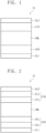
- FIG. 1 is a cross-sectional view schematically illustrating an organic electroluminescence device according to one or more embodiments of the present disclosure.
- FIG. 2 is a cross-sectional view schematically illustrating an organic electroluminescence device according to one or more embodiments of the present disclosure.
- FIG. 3 is a cross-sectional view schematically illustrating an organic electroluminescence device according to one or more embodiments of the present disclosure.
- an organic electroluminescence device (OLED) 10 includes a first electrode EL1, a hole transport region HTR, an emission layer EML, an electron transport region ETR, and a second electrode EL2.
- the first electrode EL1 has conductivity (e.g., may be conductive).
- the first electrode EL1 may be a pixel electrode or an anode.
- the first electrode EL1 may be a transmissive electrode, a transflective (e.g., semi-transmissive) electrode, or a reflective electrode.
- the first electrode EL1 may include a transparent metal oxide (such as indium tin oxide (ITO), indium zinc oxide (IZO), zinc oxide (ZnO), and/or indium tin zinc oxide (ITZO)).
- ITO indium tin oxide
- IZO indium zinc oxide
- ZnO zinc oxide
- ITZO indium tin zinc oxide
- the first electrode EL1 may include silver (Ag), magnesium (Mg), copper (Cu), aluminium (Al), platinum (Pt), palladium (Pd), gold (Au), nickel (Ni), neodymium (Nd), iridium (Ir), chromium (Cr), lithium (Li), calcium (Ca), LiF/Ca, LiF/Al, molybdenum (Mo), titanium (Ti), a compound thereof, or a mixture thereof (for example, a mixture of Ag and Mg).
- the first electrode EL1 may include a plurality of layers including a reflective layer or transflective layer formed using the above materials, or a transparent layer formed using ITO, IZO, ZnO, or ITZO.
- the first electrode EL1 may have a three-layer structure of ITO/Ag/ITO, without limitation.
- the thickness of the first electrode EL1 may be about 1,000 ⁇ to about 10,000 ⁇ , for example, about 1,000 ⁇ to about 3,000 ⁇ .
- the hole transport region HTR is on the first electrode EL1.
- the hole transport region HTR may include at least one of a hole injection layer HIL, a hole transport layer HTL, a hole buffer layer, and an electron blocking layer EBL.
- the thickness of the hole transport region HTR may be, for example, about 100 ⁇ to about 1,500 ⁇ .
- the hole transport region HTR may include a hole injection layer HIL and a hole transport layer HTL, as shown in FIG. 2 .
- the hole transport region HTR may include a hole injection layer HIL, a hole transport layer HTL, and an electron blocking layer EBL, as shown in FIG. 3 .
- the hole transport region HTR may be a single layer formed using a single material, a single layer formed using a plurality of different materials, or a multilayer structure including a plurality of layers formed using a plurality of different materials.
- the hole transport region HTR may have the structure of a single layer (such as a hole injection layer HIL and a hole transport layer HTL, e.g., together), and may have a structure of a single layer formed using a hole injection material and a hole transport material.
- a single layer such as a hole injection layer HIL and a hole transport layer HTL, e.g., together
- HTL hole transport layer
- the hole transport region HTR may have a structure of a single layer formed using a plurality of different materials, or a structure laminated on the first electrode EL1, for example, including a hole injection layer HIL/hole transport layer HTL, a hole injection layer HIL/hole transport layer HTL/hole buffer layer, a hole injection layer HIL/hole buffer layer, a hole transport layer HTL/hole buffer layer, or a hole injection layer HIL/hole transport layer HTL/electron blocking layer EBL, without limitation.
- the hole transport region HTR may be formed using one or more suitable methods (such as a vacuum deposition method, a spin coating method, a cast method, a Langmuir-Blodgett (LB) method, an inkjet printing method, a laser printing method, and/or a laser induced thermal imaging (LITI) method).
- suitable methods such as a vacuum deposition method, a spin coating method, a cast method, a Langmuir-Blodgett (LB) method, an inkjet printing method, a laser printing method, and/or a laser induced thermal imaging (LITI) method).
- the hole injection layer HIL may include, for example, a phthalocyanine compound (such as copper phthalocyanine); N,N'-diphenyl-N,N'-bis-[4-(phenyl-m-tolyl-amino)-phenyl]-biphenyl-4,4'-diamine (DNTPD), 4,4',4"-tris[(3-methylphenyl)phenylamino] triphenylamine (m-MTDATA), 4,4',4"-tris(N,N-diphenylamino)triphenylamine (TDATA), 4,4',4"-tris ⁇ N-(2-naphthyl)-N-phenylamino ⁇ -triphenylamine (2-TNATA), poly(3,4-ethylenedioxythiophene)/poly(4-styrenesulfonate) (PEDOT/PSS), polyaniline/dodecylbenzenesulfonic acid (PANI/DBSA
- the hole transport layer HTL may include, for example, carbazole derivatives (such as N-phenyl carbazole and/or polyvinyl carbazole), fluorene-based derivatives, N,N'-bis(3-methylphenyl)-N,N'-diphenyl-[1,1-biphenyl]-4,4'-diamine (TPD), triphenylamine-based derivatives (such as 4,4',4"-tris(N-carbazolyl)triphenylamine (TCTA)), N,N'-di(1-naphthalene-1-yl)-N,N'-diphenyl-benzidine (NPB), 4,4'-cyclohexylidene bis[N,N-bis(4-methylphenyl)benzenamine] (TAPC), 4,4'-bis[N,N'-(3-tolyl)amino]-3,3'-dimethylbiphenyl (HMTPD), 1,3-bis(N-car
- the thickness of the hole transport region HTR may be about 100 ⁇ to about 10,000 ⁇ , for example, about 100 ⁇ to about 7000 ⁇ , about 100 ⁇ to about 5000 ⁇ , about 100 ⁇ to about 3000 ⁇ , or about 100 ⁇ to about 1,000 ⁇ .
- the thickness of the hole injection layer HIL may be about 100 ⁇ to about 10,000 ⁇ , for example, about 100 ⁇ to about 7,000 ⁇ , about 100 ⁇ to about 5,000 ⁇ , about 100 ⁇ to about 3,000 ⁇ , about 100 ⁇ to about 2,000 ⁇ , about 100 ⁇ to about 1,000 ⁇ or about 100 ⁇ to about 200 ⁇ , and the thickness of the hole transport layer HTL may be about 30 ⁇ to about 1,000 ⁇ , about 100 ⁇ to about 1,000 ⁇ , about 500 ⁇ to about 1000 ⁇ , about 600 ⁇ to about 1000 ⁇ , or about 700 ⁇ to about 900 ⁇ .
- the thicknesses of the hole transport region HTR, the hole injection layer HIL, and the hole transport layer HTL each satisfy the above-described ranges, satisfactory hole transport properties may be obtained without a substantial increase in driving voltage.
- the hole transport region HTR may further include a charge generating material in addition to the above-described materials to increase conductivity.
- the charge generating material may be dispersed uniformly or non-uniformly in the hole transport region HTR.
- the charge generating material may be, for example, a p-dopant.
- the p-dopant may be a quinone derivative, a metal oxide, or a cyano group-containing compound, without limitation.
- Non-limiting examples of the p-dopant may include quinone derivatives (such as tetracyanoquinodimethane (TCNQ) and/or 2,3,5,6-tetrafluoro-7,7,8,8-tetracyanoquinodimethane (F4-TCNQ)), metal oxides (such as tungsten oxide and/or molybdenum oxide).
- quinone derivatives such as tetracyanoquinodimethane (TCNQ) and/or 2,3,5,6-tetrafluoro-7,7,8,8-tetracyanoquinodimethane (F4-TCNQ)
- metal oxides such as tungsten oxide and/or molybdenum oxide
- the hole transport region HTR may further include at least one of a hole buffer layer and an electron blocking layer EBL, in addition to the hole injection layer HIL and the hole transport layer HTL.
- the hole buffer layer may compensate for a resonance distance according to the wavelength of light emitted from the emission layer EML (e.g., be used to adjust the optical resonance distance to match the wavelength of light emitted from the emission layer) and to increase the light emission efficiency of the device.
- Materials included in the hole transport region HTR may also be included in the hole buffer layer.
- the electron blocking layer EBL may prevent or reduce electron injection from the electron transport region ETR to the hole transport region HTR.
- the emission layer EML may be on the hole transport region HTR.
- the emission layer EML may have a thickness of about 100 ⁇ to about 1,000 ⁇ , about 100 ⁇ to about 800 ⁇ , about 100 ⁇ to about 700 ⁇ , about 100 ⁇ to about 600 ⁇ , about 100 ⁇ to about 500 ⁇ , about 100 ⁇ to about 400 ⁇ or about 100 ⁇ to about 300 ⁇ .
- the emission layer EML may be a single layer formed using a single material, a single layer formed using a plurality of different materials, or a multilayer structure having a plurality of layers formed using a plurality of different materials.
- the emission layer EML includes a polycyclic compound according to one or more embodiments of the present disclosure.
- the polycyclic compound according to one or more embodiments of the present disclosure will be explained in more detail.
- substituted or unsubstituted may refer to substitution with at least one substituent selected from the group consisting of a deuterium atom, a halogen atom, a cyano group, a nitro group, a nitro group, an amino group, a silyl group, a boron group, a phosphine oxide group, a phosphine sulfide group, an alkyl group, an alkenyl group, an aryl group, and a heterocycle, or absence of the above substituents (e.g., substitution with hydrogen atoms only).
- each of the above substituents may be further substituted or unsubstituted.
- a biphenyl group may be interpreted as an aryl group in itself, or as a phenyl group substituted with a phenyl group.
- heterocycle as used herein may refer to aliphatic heterocycles and aromatic heterocycles (heteroaryl group).
- substituted or unsubstituted may refer to being substituted with one or more substituents selected from the group consisting of a deuterium atom, a halogen atom, a cyano group, an alkyl group, an aryl group, and a heterocycle, as well as being unsubstituted.
- halogen atom may refer to a fluorine atom (F), a chlorine atom (Cl), a bromine atom (Br), and/or an iodine atom (I).
- alkyl (e.g., “alkyl group”) may refer to a linear, branched, or cyclic alkyl group.
- the carbon number of the alkyl may be 1 to 30, 1 to 20, 1 to 10, or 1 to 5.
- Non-limiting examples of an alkyl group may include methyl, ethyl, n-propyl, isopropyl, n-butyl, s-butyl, t-butyl, i-butyl, 2-ethylbutyl, 3,3-dimethylbutyl, n-pentyl, i-pentyl, neopentyl, t-pentyl, cyclopentyl, 1-methylpentyl, 3-methylpentyl, 2-ethylpentyl, 4-methyl-2-pentyl, n-hexyl, 1-methylhexyl, 2-ethylhexyl, 2-butylhexyl, cyclohexyl, 4-methylcyclohexyl, 4-t-butylcyclohexyl, n-heptyl, 1-methylheptyl, 2,2-dimethylheptyl, 2-ethylheptyl, 2-but
- alkenyl group may refer to a linear chain (e.g., linear alkene) or a branched chain (e.g., branched alkene).
- the carbon number is not specifically limited, and for example, may be 2 to 30, 2 to 20, or 2 to 10.
- Non-limiting examples of the alkenyl group may include vinyl, 1-butenyl, 1-pentenyl, 1,3-butadienyl aryl, styrenyl, styrylvinyl, etc.
- embodiments of the present disclosure are not limited thereto.
- aryl group refers to a functional group or substituent derived from an aromatic hydrocarbon ring.
- the aryl group may be a monocyclic aryl group or a polycyclic aryl group.
- the number of carbon atoms for forming a ring in the aryl group may be 6 to 60, 6 to 30, 6 to 20, or 6 to 15.
- Non-limiting examples of the aryl group may include phenyl, naphthyl, fluorenyl, anthracenyl, phenanthryl, biphenyl, terphenyl, quaterphenyl, quinqphenyl, sexiphenyl, biphenylene, triphenylene, pyrenyl, benzofluoranthenyl, chrysenyl, etc.
- the fluorenyl group may be substituted (e.g., at the 9H position), and two substituents of the fluorenyl group may be combined with each other to form a spiro structure.
- substituted fluorenyl groups are shown below. However, embodiments of the present disclosure are not limited thereto.
- heterocycle may refer to a cyclic structure including at least one of boron (B), O, N, phosphorus (P), silicon (Si), or S as a heteroatom.
- B boron
- P phosphorus
- Si silicon
- S S
- the heterocycle may be heteroaromatic, and may be a monocyclic heteroaryl group or a polycyclic heteroaryl group.
- the number of carbons for forming a ring in the heterocycle may be 2 to 30, 2 to 20, or 2 to 10.
- Non-limiting examples of the polycycle may include thiophene, furan, pyrrole, imidazole, thiazole, oxazole, oxadiazole, triazole, pyridine, bipyridine, pyrimidine, triazine, triazole, acridyl, pyridazine, pyrazinyl, quinoline, quinazoline, quinoxaline, phenoxazine, phthalazine, pyrido pyrimidine, pyrido pyrazine, pyrazino pyrazine, isoquinoline, indole, carbazole, N-arylcarbazole, N-heteroarylcarbazole, N-alkylcarbazole, benzoxazole, benzimidazole, benzothiazole, benzocarbazole, benzothiophene, dibenzothiophene, thienothi
- silyl group may refer to an alkyl silyl group and/or an aryl silyl group.
- Non-limiting examples of the silyl group may include trimethylsilyl, triethylsilyl, t-butyldimethylsilyl, vinyldimethylsilyl, propyldimethylsilyl, triphenylsilyl, diphenylsilyl, phenylsilyl, etc.
- embodiments of the present disclosure are not limited thereto.
- the boron group includes an alkyl boron group and an aryl boron group.
- Non-limiting examples of the boron group may include trimethylboron, triethylboron, t-butyldimethylboron, triphenylboron, diphenylboron, phenylboron, etc.
- embodiments of the present disclosure are not limited thereto.
- the carbon number of the amino group is not specifically limited, and for example, may be 1 to 30.
- the amino group may include an alkyl amino group and an aryl amino group.
- Non-limiting examples of the amino group include a methylamino group, a dimethylamino group, a phenylamino group, a diphenylamino group, a naphthylamino group, a 9-methyl-anthracenylamino group, a triphenylamino group, etc.
- the phosphine oxide group may be substituted with at least one of an alkyl group or an aryl group.
- Non-limiting examples of the phosphine oxide group include a phenyl phosphine oxide group, diphenyl phosphine oxide group, etc.
- the phosphine sulfide group may be substituted with at least one of an alkyl group or an aryl group.
- the polycyclic compound according to one or more embodiments of the present disclosure is represented by Formula 1:
- X 1 is C, Si, or Ge;
- Ar is a substituted or unsubstituted aryl group having 6 to 30 carbon atoms for forming a ring, or a substituted or unsubstituted heteroaryl group having 2 to 30 carbon atoms for forming a ring;
- R 1 to R 4 are each independently a hydrogen atom (H), a deuterium atom (D), a substituted or unsubstituted alkyl group having 1 to 10 carbon atoms, a substituted or unsubstituted aryl group having 6 to 30 carbon atoms for forming a ring, or a substituted or unsubstituted heteroaryl group having 2 to 30 carbon atoms for forming a ring;
- "a" to "d” are each independently an integer of 0 to 4, and AC is represented by one of Formulae 5 to 7:
- a 1 to A 13 are each independently N or CR 15 , at least one of A 1 to A 8 is N, at least one of A 9 to A 13 is N, and at least one of A 1 to A 13 is a part that is connected with Formula 1; and R 15 is a hydrogen atom, a deuterium atom, a substituted or unsubstituted alkyl group having 1 to 10 carbon atoms, a substituted or unsubstituted aryl group having 6 to 30 carbon atoms for forming a ring, or a substituted or unsubstituted heteroaryl group having 2 to 30 carbon atoms for forming a ring.
- R 1 may not be a hydrogen atom; if "b” is 0, R 2 may not be a hydrogen atom; if “c” is 0, R 3 may not be a hydrogen atom; and if "d” is 0, R 4 may not be a hydrogen atom.
- each of "a” to “d” may be 0.
- embodiments of the present disclosure are not limited thereto.
- at least one of “a” to “d” may be 1 or more, and a substituent other than a hydrogen atom may be introduced.
- Ar may be a substituted or unsubstituted aryl group having 6 to 20 carbon atoms.
- Ar may be a substituted or unsubstituted phenyl group, a substituted or unsubstituted naphthyl group, a substituted or unsubstituted biphenyl group, a substituted or unsubstituted anthracenyl group, a substituted or unsubstituted phenanthryl group, or a substituted or unsubstituted terphenyl group.
- Ar may be a substituted or unsubstituted phenyl group.
- Ar may be an unsubstituted phenyl group.
- R 1 to R 4 may each independently be a hydrogen atom, a deuterium atom, a substituted or unsubstituted alkyl group having 1 to 5 carbon atoms, a substituted or unsubstituted aryl group having 6 to 20 carbon atoms for forming a ring, or a substituted or unsubstituted heteroaryl group having 2 to 20 carbon atoms for forming a ring.
- AC in Formula 1 is an electron acceptor
- the structure excluding AC in Formula 1 is an electron donor
- the polycyclic compound according to one or more embodiments of the present disclosure includes an electron acceptor and an electron donor in one molecule.
- R 15 may be a hydrogen atom, a deuterium atom, a substituted or unsubstituted alkyl group having 1 to 5 carbon atoms, a substituted or unsubstituted aryl group having 6 to 20 carbon atoms for forming a ring, or a substituted or unsubstituted heteroaryl group having 2 to 20 carbon atoms for forming a ring.
- R 15 may be a hydrogen atom.
- Formula 7 may be further represented by one of the following formulae, but embodiments of the present disclosure are not limited thereto:
- the polycyclic compound represented by Formula 1 may be at least one selected from the compounds represented in Compound Group 1, but embodiments of the present disclosure are not limited thereto:
- the polycyclic compound according to one or more embodiments of the present disclosure may have an energy level difference between a singlet energy level and a triplet energy level of about 0.2 eV or less, and as a result, may be utilized as a material for thermally activated delayed fluorescence.
- the polycyclic compound according to one or more embodiments of the present disclosure may be used as a material for an organic electroluminescence device to contribute to an increase in efficiency.
- the emission layer EML may include one or two or more kinds of structures of the polycyclic compound represented by Formula 1.
- the emission layer EML may further include other suitable materials in addition to the polycyclic compound represented by Formula 1.
- the emission layer EML may include a host and a dopant, and the dopant may include the polycyclic compound represented by Formula 1.
- the polycyclic compound according to one or more embodiments of the present disclosure may be included in the emission layer EML as a dopant for thermally activated delayed fluorescence.
- the polycyclic compound according to one or more embodiments of the present disclosure may be included in the emission layer EML as a dopant for emitting blue light having a wavelength of about 470 nm or less, and for example, may be included in the emission layer EML as a dopant for emitting deep blue light having a wavelength of about 440 nm to about 470 nm, or about 450 nm to about 470 nm.
- the host material may include suitable materials available in the art, without limitation.
- suitable materials available in the art, without limitation.
- DPEPO bis[2-(diphenylphosphino)phenyl] ether oxide
- CBP 4,4'-bis(carbazol-9-yl)biphenyl
- mCP 1,3-bis(carbazol-9-yl)benzene
- PPF 2,8-bis(diphenylphosphoryl)dibenzo[b,d]furan
- PPF 4,4',4"-tris(carbazol-9-yl)-triphenylamine
- TPBi 1,3,5-tris(N-phenylbenzimidazole-2-yl)benzene
- embodiments of the present disclosure are not limited thereto.
- the emission layer EML may further include at least one of N,N,N',N'-tetraphenyl-pyrene-1,6-diamine (TPD), 4,4'-bis(2-(9-ethyl-9H-carbazol-3-yl)vinyl)-1,1'-biphenyl (BCzVBi); 4,4'-bis(9-ethyl-3-carbazovinylene)-1,1'-biphenyl, 10-phenyl-10H,10'H-spiro[acridine-9,9'-anthracene]-10'-one (ACRSA), 3,4,5,6-tetra-9H-carbazol-9-yl-1,2-benzenedicarbonitrile (4CzPN), 2,4,5,6-tetra-9H-carbazol-9-yl-isophthalonitrile (4CzIPN), bis[4-9,9-dimethyl-9,10-dihydroacridine]phenyl]sulfone
- the emission layer EML may further include styryl derivatives (for example, 1,4-bis[2-(3-N-ethylcarbazoryl)vinyl]benzene (BCzVB), 4-(di-p-tolylamino)-4'-[(di-p-tolylamino)styryl]stilbene (DPAVB), and N-(4-((E)-2-(6-((E)-4-(diphenylamino)styryl)naphthalen-2-yl)vinyl)phenyl)-N-phenylbenzenamine (N-BDAVBi)), perylene and derivatives thereof (for example, 2,5,8,11-tetra-t-butylperylene (TBP)), pyrene and the derivatives thereof (for example, 1,1-dipyrene, 1,4-dipyrenylbenzene, 1,4-bis(N,N-diphenylamino)pyrene), etc.,
- the emission layer EML may be a blue emission layer to emit blue light.
- the emission layer EML may be an emission layer to emit light in a wavelength of about 480 nm or less, or about 470 nm or less.
- the emission layer EML may be a fluorescence emission layer radiating fluorescence.
- the emission layer EML may be a delayed fluorescence emission layer radiating delayed fluorescence.
- the electron transport region ETR is on the emission layer EML.
- the electron transport region ETR may include at least one of a hole blocking layer HBL, an electron transport layer ETL, or an electron injection layer EIL, without limitation.
- the electron transport region ETR may include an electron injection layer EIL and an electron transport layer ETL, as shown in FIG. 2 .
- the electron transport region ETR may include an electron injection layer EIL, an electron transport layer ETL, and hole blocking layer EBL, as shown in FIG. 3 .
- the electron transport region ETR may have or be a single layer formed using a single material, a single layer formed using a plurality of different materials, or a multilayer structure having a plurality of layers formed using a plurality of different materials.
- the electron transport region ETR may have a single layer structure of an electron injection layer EIL or an electron transport layer ETL, or a single layer structure formed using an electron injection material and an electron transport material. Further, the electron transport region ETR may have a single layer structure having a plurality of different materials, or a structure laminated from the emission layer EML of electron transport layer ETL/electron injection layer EIL, or hole blocking layer HBL/electron transport layer ETL/electron injection layer EIL, without limitation.
- the thickness of the electron transport region ETR may be, for example, from about 1,000 ⁇ to about 1,500 ⁇ .
- the electron transport region ETR may be formed using one or more suitable methods (such as a vacuum deposition method, a spin coating method, a cast method, a Langmuir-Blodgett (LB) method, an inkjet printing method, a laser printing method, and/or a laser induced thermal imaging (LITI) method).
- suitable methods such as a vacuum deposition method, a spin coating method, a cast method, a Langmuir-Blodgett (LB) method, an inkjet printing method, a laser printing method, and/or a laser induced thermal imaging (LITI) method).
- the electron transport region ETR may include an anthracene-based compound.
- the electron transport region ETR may include, for example, tris(8-hydroxyquinolinato)aluminum (Alq 3 ), 1,3,5-tri[(3-pyridyl)-phen-3-yl]benzene, 2,4,6-tris(3'-(pyridin-3-yl)biphenyl-3-yl)-1,3,5-triazine, 2-(4-(N-phenylbenzoimidazolyl-1-ylphenyl)-9,10-dinaphthylanthracene, 1,3,5-tri(1-phenyl-1H-benzo[d]imidazol-2-yl)phenyl (TPBi), 2,9-dimethyl-4,7-diphenyl-1,10-phenanthroline (BCP), 4,7-diphenyl
- the thickness of the electron transport layer ETL may be about 100 ⁇ to about 1,000 ⁇ , for example, about 100 ⁇ to about 700 ⁇ , about 100 ⁇ to about 600 ⁇ , about 150 ⁇ to about 600 ⁇ , about 150 ⁇ to about 500 ⁇ or about 250 ⁇ to about 350 ⁇ .
- the thickness of the electron transport layer ETL satisfies the above-described range, satisfactory electron transport properties may be obtained without a substantial increase in driving voltage.
- the electron transport layer ETL may use LiF, lithium quinolate (LiQ), Li 2 O, BaO, NaCl, CsF, a lanthanide metal (such as ytterbium (Yb)), or a metal halide (such as RbCI and/or Rbl).
- LiQ lithium quinolate
- Li 2 O Li 2 O
- BaO Li 2 O
- NaCl Li 2 O
- CsF lithium quinolate
- CsF lithium quinolate
- Yb lanthanide metal
- RbCI and/or Rbl metal halide
- the electron injection layer EIL may also be formed using a mixture of an electron transport material and an insulating organometallic salt.
- the organometallic salt may be a material having an energy band gap of about 4 eV or more.
- Non-limiting examples of the organometallic salt may include metal acetates, metal benzoates, metal acetoacetates, metal acetylacetonates, and metal stearates.
- the thickness of the electron injection layer EIL may be about 1 ⁇ to about 100 ⁇ , about 3 ⁇ to about 90 ⁇ or about 3 ⁇ to about 10 ⁇ . When the thickness of the electron injection layer EIL satisfies the above-described range, satisfactory electron injection properties may be obtained without substantial increase of a driving voltage.
- the electron transport region ETR may include a hole blocking layer HBL as described above.
- the hole blocking layer may include, for example, 2,9-dimethyl-4,7-diphenyl-1,10-phenanthroline (BCP), and/or 4,7-diphenyl-1,10-phenanthroline (Bphen).
- BCP 2,9-dimethyl-4,7-diphenyl-1,10-phenanthroline
- Bphen 4,7-diphenyl-1,10-phenanthroline
- embodiments of the present disclosure are not limited thereto.
- the second electrode EL2 may be on the electron transport region ETR.
- the second electrode EL2 may be a common electrode or a cathode.
- the second electrode EL2 may be a transmissive electrode, a transflective (e.g., semi-transmissive) electrode, or a reflective electrode.
- the second electrode EL2 may include a transparent metal oxide, for example, ITO, IZO, ZnO, ITZO, etc.
- the second electrode EL2 When the second electrode EL2 is a transflective electrode or a reflective electrode, the second electrode EL2 may include Ag, Mg, Cu, Al, Pt, Pd, Au, Ni, Nd, Ir, Cr, Li, Ca, LiF/Ca, LiF/Al, Mo, Ti, a compound including one or more of the listed metals, or a mixture thereof (for example, a mixture of Ag and Mg).
- the second electrode EL2 may have a multilayered structure including a reflective layer or a transflective layer formed using the above-described materials and a transparent conductive layer formed using ITO, IZO, ZnO, ITZO, etc.
- the second electrode EL2 may be connected with (to) an auxiliary electrode.
- the resistance of the second electrode EL2 may decrease.
- the organic electroluminescence device 10 during application of a voltage to each of the first electrode EL1 and second electrode EL2, holes injected from the first electrode EL1 may move via the hole transport region HTR to the emission layer EML, and electrons injected from the second electrode EL2 may move via the electron transport region ETR to the emission layer EML.
- the electrons and the holes may recombine in the emission layer EML to produce excitons, and the excitons may emit light when they transition from an excited state to the ground state.
- the first electrode EL1 When the organic electroluminescence device 10 is a top emission type (top emission OLED), the first electrode EL1 may be a reflective electrode and the second electrode EL2 may be a transmissive electrode or a transflective electrode.
- the organic electroluminescence device 10 When the organic electroluminescence device 10 is a bottom emission type (bottom emission OLED), the first electrode EL1 may be a transmissive electrode or a transflective electrode and the second electrode EL2 may be a reflective electrode.
- the organic electroluminescence device 10 may include the polycyclic compound as a material for an emission layer EML, and thus, high efficiency may be achieved.
- polycyclic compound according to one or more embodiments of the present disclosure may be synthesized, for example, as follows. However, embodiments of the present disclosure are not limited thereto.
- Reference Compound 8 according to one or more embodiments of the present disclosure may be synthesized, for example, as follows.
- Compound 40 according to one or more embodiments of the present disclosure may be synthesized, for example, as follows.
- Compound 40 was obtained in 81% yield by conducting substantially the same procedure as described in the synthetic method of Reference Compound 8, except for using Compound E instead of Compound C.
- Reference Compound 69 according to one or more embodiments of the present disclosure may be synthesized, for example, as follows.
- Reference Compound 69 was obtained in 89% yield by conducting substantially the same procedure as described in the synthetic method of Reference Compound 8, except for using Intermediate 3A instead of Intermediate 2A.
- Reference Compound 127 according to one or more embodiments of the present disclosure may be synthesized, for example, as follows.
- Reference Compound 127 was obtained in 86% yield by conducting substantially the same procedure as described in the synthetic method of Reference Compound 8, except for using Compound F instead of Compound C.
- Reference Compound 131 according to one or more embodiments of the present disclosure may be synthesized, for example, as follows.
- Reference Compound 131 was obtained in 91% yield by conducting substantially the same procedure as described in the synthetic method of Reference Compound 8, except for using Compound G instead of Compound C.
- the above-described synthetic examples are illustrations, and reaction conditions may be changed as necessary.
- the compounds according to one or more embodiments of the present disclosure may be synthesized so as to include various suitable substituents using methods and materials available in the art. Such substituents may be introduced into a core structure represented by Formula 1 to yield properties suitable for application to an organic electroluminescence device.
- Organic electroluminescence devices of Reference Examples 1 and 3 to 5, and Example 2 were manufactured using Reference Compounds 8, 69, 127 and 131, and Compound 40, respectively, as dopant materials in the emission layer of each device.
- Organic electroluminescence devices of Comparative Examples 1 to 10 were manufactured using Compounds C-1 to C-10, respectively, as dopant materials in the emission layer of each device.
- the S 1 (singlet) energy levels and T 1 (triplet) energy levels of the example compound, reference example compounds and the comparative compounds were calculated using a non-empirical molecular orbital method.
- the calculations were conducted using B3LYP as a functional, and 6-31 G(d) as a basis function in Gaussian 09 (Gaussian Co., Wallingford, CT).
- Gaussian 09 Gaussian Co., Wallingford, CT
- Example Compounds 8, 69, 127 and 131, Example Compound 40, and Comparative Compounds C-2 and C-4 to C-8 each showed low ⁇ E ST values, and are thought to exhibit thermally activated delayed fluorescence.
- Comparative Compounds C-1, C-3, C-9 and C-10 showed high ⁇ E ST values, and are not thought to exhibit thermally activated delayed fluorescence.
- Each organic electroluminescence device of Reference Examples 1 and 3 to 5, Example 2 and Comparative Examples 1 to 10 was manufactured by forming a first electrode using ITO to a thickness of about 150 nm, a hole injection layer using HAT-CN to a thickness of about 10 nm, a hole transport layer using NPB to a thickness of about 80 nm, an electron blocking layer using mCP to a thickness of about 5 nm, an emission layer using DPEPO doped with 20% of the Example Compound or the Comparative Compound to a thickness of about 20 nm, a hole blocking layer using DPEPO to a thickness of about 10 nm, an electron transport layer using TPBi to a thickness of about 30 nm, an electron injection layer using LiF to a thickness of about 0.5 nm, and a second electrode using Al to a thickness of about 100 nm. Each layer was formed using a vacuum deposition method.
- Reference Example Compounds 8, 69, 127 and 131, and Example Compound 40 all had light emission wavelengths of less than about 470 nm, and are suitable as deep blue dopants, thereby accomplishing high efficiency due to thermally activated delayed fluorescence.
- Comparative Examples 1, 6, 9 and 10 showed relatively low emission efficiencies and short emission wavelengths.
- Comparative Examples 4, 5 and 8 showed relatively high efficiencies but longer wavelengths, and deep blue light emission was not accomplished.
- Comparative Example 7 showed a wavelength near a deep blue color but with lower efficiency than the examples.
- Comparative Example 2 showed neither a deep blue color nor high efficiency. Though ⁇ E ST of the calculated value of Comparative Example 2 was small, there was a chance that thermally activated delayed fluorescence was not shown.
- Comparative Example 3 showed a low efficiency and longer wavelength, and did not show a deep blue color.
- the polycyclic compound according to one or more embodiments of the present disclosure may be utilized as a dopant of thermally activated delayed fluorescence for emitting deep blue color.
- the organic electroluminescence device including the polycyclic compound according to one or more embodiments of the present disclosure accomplishes deep blue color and has excellent efficiency at the same time.
- the organic electroluminescence device according to one or more embodiments of the present disclosure has excellent efficiency.
- the polycyclic compound according to one or more embodiments of the present disclosure may be applied to an organic electroluminescence device and may contribute to high efficiency.
- any numerical range recited herein is intended to include all subranges of the same numerical precision subsumed within the recited range.
- a range of "1.0 to 10.0" is intended to include all subranges between (and including) the recited minimum value of 1.0 and the recited maximum value of 10.0, that is, having a minimum value equal to or greater than 1.0 and a maximum value equal to or less than 10.0, such as, for example, 2.4 to 7.6.
- Any maximum numerical limitation recited herein is intended to include all lower numerical limitations subsumed therein and any minimum numerical limitation recited in this specification is intended to include all higher numerical limitations subsumed therein.
Landscapes
- Chemical & Material Sciences (AREA)
- Organic Chemistry (AREA)
- Engineering & Computer Science (AREA)
- Materials Engineering (AREA)
- Physics & Mathematics (AREA)
- Spectroscopy & Molecular Physics (AREA)
- Optics & Photonics (AREA)
- Electroluminescent Light Sources (AREA)
- Nitrogen And Oxygen Or Sulfur-Condensed Heterocyclic Ring Systems (AREA)
- Nitrogen Condensed Heterocyclic Rings (AREA)
Applications Claiming Priority (2)
| Application Number | Priority Date | Filing Date | Title |
|---|---|---|---|
| KR1020180039925A KR20190117038A (ko) | 2018-04-05 | 2018-04-05 | 유기 전계 발광 소자 및 유기 전계 발광 소자용 다환 화합물 |
| EP19163608.3A EP3549941B1 (en) | 2018-04-05 | 2019-03-19 | Organic electroluminescence device and polycyclic compound for organic electroluminescence device |
Related Parent Applications (1)
| Application Number | Title | Priority Date | Filing Date |
|---|---|---|---|
| EP19163608.3A Division EP3549941B1 (en) | 2018-04-05 | 2019-03-19 | Organic electroluminescence device and polycyclic compound for organic electroluminescence device |
Publications (2)
| Publication Number | Publication Date |
|---|---|
| EP3978495A1 EP3978495A1 (en) | 2022-04-06 |
| EP3978495B1 true EP3978495B1 (en) | 2023-05-10 |
Family
ID=65818420
Family Applications (2)
| Application Number | Title | Priority Date | Filing Date |
|---|---|---|---|
| EP19163608.3A Active EP3549941B1 (en) | 2018-04-05 | 2019-03-19 | Organic electroluminescence device and polycyclic compound for organic electroluminescence device |
| EP21203301.3A Active EP3978495B1 (en) | 2018-04-05 | 2019-03-19 | Organic electroluminescence device and polycyclic compound for organic electroluminescence device |
Family Applications Before (1)
| Application Number | Title | Priority Date | Filing Date |
|---|---|---|---|
| EP19163608.3A Active EP3549941B1 (en) | 2018-04-05 | 2019-03-19 | Organic electroluminescence device and polycyclic compound for organic electroluminescence device |
Country Status (5)
| Country | Link |
|---|---|
| US (1) | US20190312210A1 (ko) |
| EP (2) | EP3549941B1 (ko) |
| JP (2) | JP2019182843A (ko) |
| KR (1) | KR20190117038A (ko) |
| CN (2) | CN110343105B (ko) |
Families Citing this family (8)
| Publication number | Priority date | Publication date | Assignee | Title |
|---|---|---|---|---|
| KR102648402B1 (ko) * | 2018-06-12 | 2024-03-18 | 삼성디스플레이 주식회사 | 축합환 화합물 및 이를 포함한 유기 발광 소자 |
| US20210159424A1 (en) * | 2019-11-26 | 2021-05-27 | Wuhan China Star Optoelectronics Semiconductor Display Technology Co., Ltd. | Hole transporting material using spirobiacridine as core and organic light emitting diode |
| CN110950866B (zh) * | 2019-11-26 | 2023-06-27 | 武汉华星光电半导体显示技术有限公司 | 以螺双吖啶为核的空穴传输材料及有机发光二极管 |
| CN112812115B (zh) * | 2020-02-28 | 2022-03-29 | 广东聚华印刷显示技术有限公司 | 吖啶类化合物、聚合物及其应用、发光器件 |
| CN111378438B (zh) * | 2020-03-18 | 2021-09-21 | 中国科学院长春应用化学研究所 | 含有芳基硼受体和空间电荷转移发光的荧光高分子化合物、制备方法及有机电致发光器件 |
| CN113620973B (zh) * | 2021-07-16 | 2024-05-07 | 西北工业大学 | 一种热活化延迟荧光材料及其制备方法和应用 |
| CN113816960A (zh) * | 2021-09-28 | 2021-12-21 | 浙江华显光电科技有限公司 | 有机化合物及包括该化合物的有机电致发光器件 |
| CN117964635A (zh) * | 2024-04-02 | 2024-05-03 | 大连理工大学 | 一种基于螺式硫杂蒽的有机发光材料及其制备方法和应用 |
Family Cites Families (8)
| Publication number | Priority date | Publication date | Assignee | Title |
|---|---|---|---|---|
| US8586210B2 (en) * | 2008-09-24 | 2013-11-19 | Hodogaya Chemical Co., Ltd. | Compound having substituted anthracene ring structure and pyridoindole ring structure and organic electroluminescence device |
| KR101779913B1 (ko) * | 2010-04-01 | 2017-09-20 | 에스에프씨 주식회사 | 스피로 화합물 및 이를 포함하는 유기전계발광소자 |
| KR101825381B1 (ko) * | 2010-04-28 | 2018-03-23 | 에스에프씨 주식회사 | 스피로 화합물 및 이를 포함하는 유기전계발광소자 |
| WO2015158411A1 (de) * | 2014-04-14 | 2015-10-22 | Merck Patent Gmbh | Materialien für elektronische vorrichtungen |
| KR101929860B1 (ko) * | 2015-05-15 | 2018-12-17 | 삼성에스디아이 주식회사 | 유기광전자소자 및 표시장치 |
| CN106831773A (zh) * | 2017-01-05 | 2017-06-13 | 华南理工大学 | 含9,9’‑螺吖啶的化合物及其制备方法和应用 |
| KR102112411B1 (ko) * | 2017-09-28 | 2020-05-18 | 주식회사 엘지화학 | 화합물 및 이를 포함하는 유기 발광 소자 |
| CN109438446A (zh) * | 2018-12-28 | 2019-03-08 | 上海天马有机发光显示技术有限公司 | 一种电致发光化合物、oled显示面板及电子设备 |
-
2018
- 2018-04-05 KR KR1020180039925A patent/KR20190117038A/ko active IP Right Grant
-
2019
- 2019-03-08 CN CN201910175195.6A patent/CN110343105B/zh active Active
- 2019-03-08 CN CN202311255810.7A patent/CN117327071A/zh active Pending
- 2019-03-11 US US16/298,942 patent/US20190312210A1/en active Pending
- 2019-03-19 EP EP19163608.3A patent/EP3549941B1/en active Active
- 2019-03-19 EP EP21203301.3A patent/EP3978495B1/en active Active
- 2019-03-26 JP JP2019059048A patent/JP2019182843A/ja active Pending
-
2023
- 2023-10-13 JP JP2023177566A patent/JP2024020205A/ja active Pending
Also Published As
| Publication number | Publication date |
|---|---|
| CN110343105B (zh) | 2023-10-24 |
| JP2024020205A (ja) | 2024-02-14 |
| EP3549941A3 (en) | 2019-11-20 |
| CN117327071A (zh) | 2024-01-02 |
| KR20190117038A (ko) | 2019-10-16 |
| EP3978495A1 (en) | 2022-04-06 |
| EP3549941A2 (en) | 2019-10-09 |
| US20190312210A1 (en) | 2019-10-10 |
| EP3549941B1 (en) | 2021-10-20 |
| JP2019182843A (ja) | 2019-10-24 |
| CN110343105A (zh) | 2019-10-18 |
Similar Documents
| Publication | Publication Date | Title |
|---|---|---|
| EP3978495B1 (en) | Organic electroluminescence device and polycyclic compound for organic electroluminescence device | |
| EP3587415B1 (en) | Organic electroluminescence device and heterocyclic compound for organic electroluminescence device | |
| EP3543230B1 (en) | Organic electroluminescence device and polycyclic compound for organic electroluminescence device | |
| EP3754736B1 (en) | Organic electroluminescence device and fused polycyclic compound for organic electroluminescence device | |
| KR102567881B1 (ko) | 함질소 화합물 및 이를 포함하는 유기 전계 발광 소자 | |
| US11462690B2 (en) | Organic electroluminescence device and polycyclic compound for organic electroluminescence device | |
| EP3653606A1 (en) | Organic electroluminescence device and compound for organic electroluminescence device | |
| EP3476842B1 (en) | Compound including nitrogen and organic electroluminescence device including the same | |
| KR102399932B1 (ko) | 열 활성 지연 형광용 화합물 및 이를 포함하는 유기 전계 발광 소자 | |
| EP3476847B1 (en) | Nitrogen-containing compound and organic electroluminescence device including the same | |
| KR102485831B1 (ko) | 함질소 화합물 및 이를 포함하는 유기 전계 발광 소자 | |
| KR20210002265A (ko) | 유기 전계 발광 소자 및 유기 전계 발광 소자용 다환 화합물 | |
| US11165026B2 (en) | Heterocyclic compound and organic electroluminescence device including the same | |
| EP3663300B1 (en) | Organic electroluminescence device and polycyclic compound for organic electroluminescence device | |
| EP3508490B1 (en) | Organic electroluminescence device and polycyclic compound for organic electroluminescence device | |
| EP3460863B1 (en) | Compound including nitrogen and organic electroluminescence device including the same | |
| KR20210099678A (ko) | 유기 전계 발광 소자 및 유기 전계 발광 소자용 다환 화합물 | |
| KR20200145945A (ko) | 유기 전계 발광 소자 및 유기 전계 발광 소자용 화합물 | |
| KR20210028313A (ko) | 유기 전계 발광 소자 및 유기 전계 발광 소자용 다환 화합물 | |
| KR102666847B1 (ko) | 유기 전계 발광 소자 및 유기 전계 발광 소자용 함질소 화합물 | |
| KR102668795B1 (ko) | 유기 전계 발광 소자 및 유기 전계 발광 소자용 다환 화합물 | |
| KR20200005698A (ko) | 유기 전계 발광 소자 및 유기 전계 발광 소자용 함질소 화합물 |
Legal Events
| Date | Code | Title | Description |
|---|---|---|---|
| PUAI | Public reference made under article 153(3) epc to a published international application that has entered the european phase |
Free format text: ORIGINAL CODE: 0009012 |
|
| STAA | Information on the status of an ep patent application or granted ep patent |
Free format text: STATUS: THE APPLICATION HAS BEEN PUBLISHED |
|
| AC | Divisional application: reference to earlier application |
Ref document number: 3549941 Country of ref document: EP Kind code of ref document: P |
|
| AK | Designated contracting states |
Kind code of ref document: A1 Designated state(s): AL AT BE BG CH CY CZ DE DK EE ES FI FR GB GR HR HU IE IS IT LI LT LU LV MC MK MT NL NO PL PT RO RS SE SI SK SM TR |
|
| STAA | Information on the status of an ep patent application or granted ep patent |
Free format text: STATUS: REQUEST FOR EXAMINATION WAS MADE |
|
| STAA | Information on the status of an ep patent application or granted ep patent |
Free format text: STATUS: EXAMINATION IS IN PROGRESS |
|
| 17P | Request for examination filed |
Effective date: 20220610 |
|
| RBV | Designated contracting states (corrected) |
Designated state(s): AL AT BE BG CH CY CZ DE DK EE ES FI FR GB GR HR HU IE IS IT LI LT LU LV MC MK MT NL NO PL PT RO RS SE SI SK SM TR |
|
| 17Q | First examination report despatched |
Effective date: 20220706 |
|
| GRAP | Despatch of communication of intention to grant a patent |
Free format text: ORIGINAL CODE: EPIDOSNIGR1 |
|
| STAA | Information on the status of an ep patent application or granted ep patent |
Free format text: STATUS: GRANT OF PATENT IS INTENDED |
|
| INTG | Intention to grant announced |
Effective date: 20221216 |
|
| RAP3 | Party data changed (applicant data changed or rights of an application transferred) |
Owner name: SAMSUNG DISPLAY CO., LTD. |
|
| GRAS | Grant fee paid |
Free format text: ORIGINAL CODE: EPIDOSNIGR3 |
|
| GRAA | (expected) grant |
Free format text: ORIGINAL CODE: 0009210 |
|
| STAA | Information on the status of an ep patent application or granted ep patent |
Free format text: STATUS: THE PATENT HAS BEEN GRANTED |
|
| AC | Divisional application: reference to earlier application |
Ref document number: 3549941 Country of ref document: EP Kind code of ref document: P |
|
| AK | Designated contracting states |
Kind code of ref document: B1 Designated state(s): AL AT BE BG CH CY CZ DE DK EE ES FI FR GB GR HR HU IE IS IT LI LT LU LV MC MK MT NL NO PL PT RO RS SE SI SK SM TR |
|
| REG | Reference to a national code |
Ref country code: GB Ref legal event code: FG4D |
|
| REG | Reference to a national code |
Ref country code: AT Ref legal event code: REF Ref document number: 1566570 Country of ref document: AT Kind code of ref document: T Effective date: 20230515 Ref country code: CH Ref legal event code: EP |
|
| REG | Reference to a national code |
Ref country code: DE Ref legal event code: R096 Ref document number: 602019028987 Country of ref document: DE |
|
| REG | Reference to a national code |
Ref country code: IE Ref legal event code: FG4D |
|
| P01 | Opt-out of the competence of the unified patent court (upc) registered |
Effective date: 20230516 |
|
| REG | Reference to a national code |
Ref country code: LT Ref legal event code: MG9D |
|
| REG | Reference to a national code |
Ref country code: NL Ref legal event code: MP Effective date: 20230510 |
|
| REG | Reference to a national code |
Ref country code: AT Ref legal event code: MK05 Ref document number: 1566570 Country of ref document: AT Kind code of ref document: T Effective date: 20230510 |
|
| PG25 | Lapsed in a contracting state [announced via postgrant information from national office to epo] |
Ref country code: SE Free format text: LAPSE BECAUSE OF FAILURE TO SUBMIT A TRANSLATION OF THE DESCRIPTION OR TO PAY THE FEE WITHIN THE PRESCRIBED TIME-LIMIT Effective date: 20230510 Ref country code: PT Free format text: LAPSE BECAUSE OF FAILURE TO SUBMIT A TRANSLATION OF THE DESCRIPTION OR TO PAY THE FEE WITHIN THE PRESCRIBED TIME-LIMIT Effective date: 20230911 Ref country code: NO Free format text: LAPSE BECAUSE OF FAILURE TO SUBMIT A TRANSLATION OF THE DESCRIPTION OR TO PAY THE FEE WITHIN THE PRESCRIBED TIME-LIMIT Effective date: 20230810 Ref country code: NL Free format text: LAPSE BECAUSE OF FAILURE TO SUBMIT A TRANSLATION OF THE DESCRIPTION OR TO PAY THE FEE WITHIN THE PRESCRIBED TIME-LIMIT Effective date: 20230510 Ref country code: ES Free format text: LAPSE BECAUSE OF FAILURE TO SUBMIT A TRANSLATION OF THE DESCRIPTION OR TO PAY THE FEE WITHIN THE PRESCRIBED TIME-LIMIT Effective date: 20230510 Ref country code: AT Free format text: LAPSE BECAUSE OF FAILURE TO SUBMIT A TRANSLATION OF THE DESCRIPTION OR TO PAY THE FEE WITHIN THE PRESCRIBED TIME-LIMIT Effective date: 20230510 |
|
| PG25 | Lapsed in a contracting state [announced via postgrant information from national office to epo] |
Ref country code: RS Free format text: LAPSE BECAUSE OF FAILURE TO SUBMIT A TRANSLATION OF THE DESCRIPTION OR TO PAY THE FEE WITHIN THE PRESCRIBED TIME-LIMIT Effective date: 20230510 Ref country code: PL Free format text: LAPSE BECAUSE OF FAILURE TO SUBMIT A TRANSLATION OF THE DESCRIPTION OR TO PAY THE FEE WITHIN THE PRESCRIBED TIME-LIMIT Effective date: 20230510 Ref country code: LV Free format text: LAPSE BECAUSE OF FAILURE TO SUBMIT A TRANSLATION OF THE DESCRIPTION OR TO PAY THE FEE WITHIN THE PRESCRIBED TIME-LIMIT Effective date: 20230510 Ref country code: LT Free format text: LAPSE BECAUSE OF FAILURE TO SUBMIT A TRANSLATION OF THE DESCRIPTION OR TO PAY THE FEE WITHIN THE PRESCRIBED TIME-LIMIT Effective date: 20230510 Ref country code: IS Free format text: LAPSE BECAUSE OF FAILURE TO SUBMIT A TRANSLATION OF THE DESCRIPTION OR TO PAY THE FEE WITHIN THE PRESCRIBED TIME-LIMIT Effective date: 20230910 Ref country code: HR Free format text: LAPSE BECAUSE OF FAILURE TO SUBMIT A TRANSLATION OF THE DESCRIPTION OR TO PAY THE FEE WITHIN THE PRESCRIBED TIME-LIMIT Effective date: 20230510 Ref country code: GR Free format text: LAPSE BECAUSE OF FAILURE TO SUBMIT A TRANSLATION OF THE DESCRIPTION OR TO PAY THE FEE WITHIN THE PRESCRIBED TIME-LIMIT Effective date: 20230811 |
|
| PG25 | Lapsed in a contracting state [announced via postgrant information from national office to epo] |
Ref country code: FI Free format text: LAPSE BECAUSE OF FAILURE TO SUBMIT A TRANSLATION OF THE DESCRIPTION OR TO PAY THE FEE WITHIN THE PRESCRIBED TIME-LIMIT Effective date: 20230510 |
|
| PG25 | Lapsed in a contracting state [announced via postgrant information from national office to epo] |
Ref country code: SK Free format text: LAPSE BECAUSE OF FAILURE TO SUBMIT A TRANSLATION OF THE DESCRIPTION OR TO PAY THE FEE WITHIN THE PRESCRIBED TIME-LIMIT Effective date: 20230510 |
|
| PG25 | Lapsed in a contracting state [announced via postgrant information from national office to epo] |
Ref country code: SM Free format text: LAPSE BECAUSE OF FAILURE TO SUBMIT A TRANSLATION OF THE DESCRIPTION OR TO PAY THE FEE WITHIN THE PRESCRIBED TIME-LIMIT Effective date: 20230510 Ref country code: SK Free format text: LAPSE BECAUSE OF FAILURE TO SUBMIT A TRANSLATION OF THE DESCRIPTION OR TO PAY THE FEE WITHIN THE PRESCRIBED TIME-LIMIT Effective date: 20230510 Ref country code: RO Free format text: LAPSE BECAUSE OF FAILURE TO SUBMIT A TRANSLATION OF THE DESCRIPTION OR TO PAY THE FEE WITHIN THE PRESCRIBED TIME-LIMIT Effective date: 20230510 Ref country code: EE Free format text: LAPSE BECAUSE OF FAILURE TO SUBMIT A TRANSLATION OF THE DESCRIPTION OR TO PAY THE FEE WITHIN THE PRESCRIBED TIME-LIMIT Effective date: 20230510 Ref country code: DK Free format text: LAPSE BECAUSE OF FAILURE TO SUBMIT A TRANSLATION OF THE DESCRIPTION OR TO PAY THE FEE WITHIN THE PRESCRIBED TIME-LIMIT Effective date: 20230510 Ref country code: CZ Free format text: LAPSE BECAUSE OF FAILURE TO SUBMIT A TRANSLATION OF THE DESCRIPTION OR TO PAY THE FEE WITHIN THE PRESCRIBED TIME-LIMIT Effective date: 20230510 |
|
| REG | Reference to a national code |
Ref country code: DE Ref legal event code: R097 Ref document number: 602019028987 Country of ref document: DE |
|
| PLBE | No opposition filed within time limit |
Free format text: ORIGINAL CODE: 0009261 |
|
| STAA | Information on the status of an ep patent application or granted ep patent |
Free format text: STATUS: NO OPPOSITION FILED WITHIN TIME LIMIT |
|
| 26N | No opposition filed |
Effective date: 20240213 |
|
| PGFP | Annual fee paid to national office [announced via postgrant information from national office to epo] |
Ref country code: DE Payment date: 20240220 Year of fee payment: 6 Ref country code: GB Payment date: 20240220 Year of fee payment: 6 |
|
| PG25 | Lapsed in a contracting state [announced via postgrant information from national office to epo] |
Ref country code: SI Free format text: LAPSE BECAUSE OF FAILURE TO SUBMIT A TRANSLATION OF THE DESCRIPTION OR TO PAY THE FEE WITHIN THE PRESCRIBED TIME-LIMIT Effective date: 20230510 |