EP3937232B1 - Architektur von induktiver verdrahtung, integrierte schaltung und kommunikationsvorrichtung - Google Patents
Architektur von induktiver verdrahtung, integrierte schaltung und kommunikationsvorrichtung Download PDFInfo
- Publication number
- EP3937232B1 EP3937232B1 EP19923130.9A EP19923130A EP3937232B1 EP 3937232 B1 EP3937232 B1 EP 3937232B1 EP 19923130 A EP19923130 A EP 19923130A EP 3937232 B1 EP3937232 B1 EP 3937232B1
- Authority
- EP
- European Patent Office
- Prior art keywords
- metal layer
- inductor device
- dummy metals
- inductor
- dummy
- Prior art date
- Legal status (The legal status is an assumption and is not a legal conclusion. Google has not performed a legal analysis and makes no representation as to the accuracy of the status listed.)
- Active
Links
Images


Classifications
-
- H—ELECTRICITY
- H10—SEMICONDUCTOR DEVICES; ELECTRIC SOLID-STATE DEVICES NOT OTHERWISE PROVIDED FOR
- H10W—GENERIC PACKAGES, INTERCONNECTIONS, CONNECTORS OR OTHER CONSTRUCTIONAL DETAILS OF DEVICES COVERED BY CLASS H10
- H10W20/00—Interconnections in chips, wafers or substrates
- H10W20/40—Interconnections external to wafers or substrates, e.g. back-end-of-line [BEOL] metallisations or vias connecting to gate electrodes
- H10W20/41—Interconnections external to wafers or substrates, e.g. back-end-of-line [BEOL] metallisations or vias connecting to gate electrodes characterised by their conductive parts
- H10W20/435—Cross-sectional shapes or dispositions of interconnections
-
- H—ELECTRICITY
- H01—ELECTRIC ELEMENTS
- H01F—MAGNETS; INDUCTANCES; TRANSFORMERS; SELECTION OF MATERIALS FOR THEIR MAGNETIC PROPERTIES
- H01F17/00—Fixed inductances of the signal type
- H01F17/0006—Printed inductances
-
- H—ELECTRICITY
- H10—SEMICONDUCTOR DEVICES; ELECTRIC SOLID-STATE DEVICES NOT OTHERWISE PROVIDED FOR
- H10D—INORGANIC ELECTRIC SEMICONDUCTOR DEVICES
- H10D1/00—Resistors, capacitors or inductors
- H10D1/20—Inductors
-
- H—ELECTRICITY
- H10—SEMICONDUCTOR DEVICES; ELECTRIC SOLID-STATE DEVICES NOT OTHERWISE PROVIDED FOR
- H10W—GENERIC PACKAGES, INTERCONNECTIONS, CONNECTORS OR OTHER CONSTRUCTIONAL DETAILS OF DEVICES COVERED BY CLASS H10
- H10W20/00—Interconnections in chips, wafers or substrates
- H10W20/40—Interconnections external to wafers or substrates, e.g. back-end-of-line [BEOL] metallisations or vias connecting to gate electrodes
- H10W20/41—Interconnections external to wafers or substrates, e.g. back-end-of-line [BEOL] metallisations or vias connecting to gate electrodes characterised by their conductive parts
- H10W20/42—Vias, e.g. via plugs
-
- H—ELECTRICITY
- H10—SEMICONDUCTOR DEVICES; ELECTRIC SOLID-STATE DEVICES NOT OTHERWISE PROVIDED FOR
- H10W—GENERIC PACKAGES, INTERCONNECTIONS, CONNECTORS OR OTHER CONSTRUCTIONAL DETAILS OF DEVICES COVERED BY CLASS H10
- H10W20/00—Interconnections in chips, wafers or substrates
- H10W20/40—Interconnections external to wafers or substrates, e.g. back-end-of-line [BEOL] metallisations or vias connecting to gate electrodes
- H10W20/41—Interconnections external to wafers or substrates, e.g. back-end-of-line [BEOL] metallisations or vias connecting to gate electrodes characterised by their conductive parts
- H10W20/43—Layouts of interconnections
-
- H—ELECTRICITY
- H10—SEMICONDUCTOR DEVICES; ELECTRIC SOLID-STATE DEVICES NOT OTHERWISE PROVIDED FOR
- H10W—GENERIC PACKAGES, INTERCONNECTIONS, CONNECTORS OR OTHER CONSTRUCTIONAL DETAILS OF DEVICES COVERED BY CLASS H10
- H10W20/00—Interconnections in chips, wafers or substrates
- H10W20/40—Interconnections external to wafers or substrates, e.g. back-end-of-line [BEOL] metallisations or vias connecting to gate electrodes
- H10W20/497—Inductive arrangements or effects of, or between, wiring layers
-
- H—ELECTRICITY
- H01—ELECTRIC ELEMENTS
- H01F—MAGNETS; INDUCTANCES; TRANSFORMERS; SELECTION OF MATERIALS FOR THEIR MAGNETIC PROPERTIES
- H01F17/00—Fixed inductances of the signal type
- H01F17/0006—Printed inductances
- H01F2017/0046—Printed inductances with a conductive path having a bridge
-
- H—ELECTRICITY
- H01—ELECTRIC ELEMENTS
- H01F—MAGNETS; INDUCTANCES; TRANSFORMERS; SELECTION OF MATERIALS FOR THEIR MAGNETIC PROPERTIES
- H01F17/00—Fixed inductances of the signal type
- H01F17/0006—Printed inductances
- H01F2017/0073—Printed inductances with a special conductive pattern, e.g. flat spiral
-
- H—ELECTRICITY
- H01—ELECTRIC ELEMENTS
- H01F—MAGNETS; INDUCTANCES; TRANSFORMERS; SELECTION OF MATERIALS FOR THEIR MAGNETIC PROPERTIES
- H01F17/00—Fixed inductances of the signal type
- H01F17/0006—Printed inductances
- H01F2017/008—Electric or magnetic shielding of printed inductances
Definitions
- This application relates to the field of integrated circuit technologies, and in particular, to an inductor device wiring architecture, an integrated circuit, and a communications device.
- the radio frequency integrated circuit may be an integrated circuit operating within a frequency range of 300 megahertz (MHz) to 300 gigahertz (GHz).
- MHz megahertz
- GHz gigahertz
- a signal frequency greatly increases. This brings faster communication experience to people, and also brings greater challenges and opportunities to the radio frequency integrated circuit.
- a plurality of layers of electronic components are connected through metal wires to form a complete logic circuit.
- CMP chemical mechanical polishing
- a common practice is to add a dummy metal (dummy metal) to a bottom metal of the metal wire to increase the metal arrangement area.
- a dummy metal dummy metal
- the dummy metal under the inductor device affects performance of the inductor device, thereby resulting in poor performance of the inductor device.
- CN 102 270 625 A discloses a dummy metal filling structure including multiple dummy metal layers, wherein each dummy metal layer includes a plurality of dummy metals, and the dummy metal in each dummy metal layer is the same as the phase.
- the dummy metals in the adjacent dummy metal layers are arranged crosswise, so that the dummy metals are distributed more uniformly, and the influence of the dummy metals on the performance of the integrated circuit is reduced.
- US 2018/047667 A1 discloses a semiconductor device with a SOI substrate including a semiconductor substrate, a BOX layer on the semiconductor substrate, and a semiconductor layer on the BOX layer, a multilayer wiring formed over a main surface of the SOI substrate, and an inductor comprised of the multilayer wiring.
- US 2008/272495 A1 discloses a semiconductor device including high-frequency interconnect and dummy conductor patterns (second dummy conductor patterns).
- the dummy conductor patterns are disposed in a interconnect layer different from a interconnect layer in which the high-frequency interconnect is disposed.
- the dummy conductor patterns are disposed so as to keep away from a region overlapping the high-frequency interconnect in plan view.
- WO 2018/052579 A1 discloses a partial metal fill within the footprint of an ultra-thick-metal (UTM) conductor on a dielectric layer to strengthen the dielectric layer to inhibit delamination of the UTM conductor without inducing significant electrical coupling between the UTM conductor and the partial metal fill.
- UTM ultra-thick-metal
- An inductor wiring architecture is disclosed as recited in claim 1.
- An integrated circuit is disclosed as recited in claim 12.
- a communication device is disclosed as recited in claim 13.
- an embodiment of this application provides an inductor device wiring architecture.
- the inductor device wiring architecture may be applied to an integrated circuit.
- the inductor device wiring architecture includes an inductor device and a plurality of dummy metals located under the inductor device.
- the plurality of dummy metals are arranged in a plurality of metal layers. Each of the plurality of metal layers corresponds to some of the plurality of dummy metals.
- Arrangement areas of dummy metals corresponding to at least three adjacent metal layers of the plurality of metal layers progressively increase in a direction away from the inductor device. In other words, arrangement areas of dummy metals corresponding to at least three adjacent metal layers located under the inductor device progressively increase.
- the arrangement areas of the dummy metals corresponding to the at least three adjacent metal layers of the plurality of metal layers under the inductor device progressively increase in the direction away from the inductor device.
- an arrangement area of dummy metals corresponding to a metal layer close to the inductor device is smaller, and an arrangement area of dummy metals corresponding to a metal layer away from the inductor device is larger.
- each metal layer under the inductor device has a relatively sufficient metal arrangement area. This can meet a processing requirement of chemical mechanical polishing, thereby improving processing quality, and achieving a higher product yield of the inductor device wiring architecture and the integrated circuit in which the inductor device wiring architecture is used.
- a space under the inductor device includes a space in which a wiring region of the inductor device is projected along a vertical direction of a metal layer in which the inductor device is located.
- the wiring region of the inductor device includes at least a region surrounded by an outer edge of an outermost wire of the inductor device.
- the plurality of dummy metals are arranged in a stepped shape.
- a dummy metal corresponding to a lower metal layer extends out relative to a dummy metal corresponding to an upper metal layer to form a stepped shape.
- the plurality of dummy metals under the inductor device are arranged in the stepped shape, the plurality of dummy metals can effectively improve metal arrangement under the inductor device, so that higher manufacturing precision of the inductor device is high during chemical mechanical polishing, and a product yield of the inductor device wiring architecture and the integrated circuit in which the inductor device wiring architecture is used is higher.
- the plurality of dummy metals can be arranged not in a region close to the inductor device, but arranged in a region away from the inductor device as far as possible, thereby reducing adverse effects of the dummy metals on performance of the inductor device, and improving performance of the inductor device.
- the inductor device wiring architecture may further include a plurality of dummy metals arranged in a same layer as that of the inductor device. Some dummy metals arranged in the same layer as that of the inductor device may be jointly arranged in a stepped shape with the plurality of dummy metals located under the inductor device. In this case, the dummy metals arranged in the same layer as that of the inductor device have less impact on performance of the inductor device, processing quality of the inductor device is higher, and a product yield of the inductor device wiring architecture is higher.
- the plurality of dummy metals under the inductor device present a continuous stepped shape. This helps further improve processing quality of the inductor device wiring architecture, and the plurality of dummy metals have less impact on performance of the inductor device.
- an arrangement area of dummy metals corresponding to an i th metal layer under the inductor device is the same as an arrangement area of dummy metals corresponding to an (i - 1) th metal layer, the i th metal layer is located on a side, of the (i - 1) th metal layer, that is away from the inductor device, and i is an integer greater than or equal to 2.
- the inductor device wiring architecture when the inductor device wiring architecture roughly meets an arrangement rule of transitioning from a sparse arrangement to a dense arrangement, two metal layers corresponding to dummy metals with a same arrangement area are included under the inductor device, so that arrangement flexibility of the plurality of dummy metals in the inductor device wiring architecture is higher, and arrangement manners are more diversified.
- the inductor device wiring architecture may include one group of two metal layers corresponding to dummy metals with a same arrangement area, or may include more than two (including two) groups of two metal layers corresponding to dummy metals with a same arrangement area. Alternatively, the inductor device wiring architecture may include more than three (including three) metal layers corresponding to dummy metals with a same arrangement area.
- a plurality of dummy metals corresponding to the i th metal layer are arranged at equal spacings, and an arrangement spacing between two adjacent dummy metals is an i th spacing; a plurality of dummy metals corresponding to the (i - 1) th metal layer are arranged at equal spacings, and an arrangement spacing between two adjacent dummy metals is an (i - 1) th spacing; and the (i - 1) th spacing is less than the i th spacing.
- metal arrangement areas of the i th metal layer do not progressively increase, the plurality of dummy metals corresponding to the i th metal layer have a larger arrangement range and a more uniform arrangement. This effectively improves processing quality of the metal layer, and achieves a higher product yield of the inductor device wiring architecture.
- an arrangement area of dummy metals corresponding to a j th metal layer under the inductor device is smaller than an arrangement area of dummy metals corresponding to a (j - 1) th metal layer, the j th metal layer is located on a side, of the (j - 1) th metal layer, that is away from the inductor device, and j is an integer greater than or equal to 2.
- the inductor device wiring architecture when the inductor device wiring architecture roughly meets an arrangement rule of transitioning from a sparse arrangement to a dense arrangement, two metal layers corresponding to dummy metals are included under the inductor device, where an arrangement area of an upper metal layer is smaller than an arrangement area of a lower metal layer, so that arrangement flexibility of the plurality of dummy metals in the inductor device wiring architecture is higher, and arrangement manners are more diversified.
- the inductor device wiring architecture may include one group of two metal layers corresponding to dummy metals, or may include more than two (including two) groups of two metal layers corresponding to dummy metals, where an arrangement area of an upper metal layer is smaller than an arrangement area of a lower metal layer.
- the inductor device wiring architecture may include more than three (including three) metal layers corresponding to dummy metals, where an arrangement area of an upper metal layer is smaller than an arrangement area of a lower metal layer.
- a plurality of dummy metals corresponding to the j th metal layer are arranged at equal spacings, and an arrangement spacing between two adjacent dummy metals is a j th spacing; a plurality of dummy metals corresponding to the (j - 1) th metal layer are arranged at equal spacings, and an arrangement spacing between two adjacent dummy metals is a (j - 1) th spacing; and the (j - 1) th spacing is less than the j th spacing.
- the plurality of dummy metals corresponding to the j th metal layer with a smaller metal arrangement area have a larger arrangement range and a more uniform arrangement. This effectively improves processing quality of the metal layer, and achieves a higher product yield of the inductor device wiring architecture.
- each metal layer corresponds to a plurality of dummy metals, and dummy metals corresponding to each metal layer are arranged in a staggered manner with dummy metals corresponding to an adjacent metal layer.
- the plurality of dummy metals under the inductor device are arranged more regularly, thereby helping reduce design costs and production costs of the inductor device wiring architecture.
- each metal layer (a metal layer of the plurality of metal layers) has a plurality of dummy metals, and dummy metals corresponding to each metal layer are arranged in alignment with dummy metals corresponding to an adjacent metal layer.
- the plurality of dummy metals under the inductor device are arranged more regularly, thereby helping reduce design costs and production costs of the inductor device wiring architecture.
- each metal layer corresponds to a plurality of dummy metals
- dummy metals corresponding to one or more metal layers are arranged in a staggered manner with dummy metals corresponding to an adjacent metal layer
- dummy metals corresponding to one or more metal layers are arranged in alignment with dummy metals corresponding to an adjacent metal layer.
- the inductor device is an inductor with two ports or a transformer with four ports.
- the inductor with two ports includes but is not limited to a helical inductor, a differential inductor, and the like.
- the inductor device may have a plurality of implementation structures, and the inductor device wiring architecture has a wider application scope.
- the inductor device is arranged in one metal layer; or the inductor device includes an upper inductor and a lower inductor, and the upper inductor and the lower inductor are arranged in two adjacent metal layers.
- the upper inductor and the lower inductor may be connected by using a conductive material, so that the inductor device serves as a multilayer metal serial inductor.
- the inductor device may have a plurality of implementation structures, and the inductor device wiring architecture has a wider application scope.
- an embodiment of this application further provides an integrated circuit, including the inductor device wiring architecture according to any one of the foregoing implementations. Because the inductor device wiring architecture has lower costs and has a little adverse effect on performance of an inductor device, the integrated circuit has low costs and high performance.
- an embodiment of this application further provides a communications device, including the foregoing integrated circuit.
- the communications device may be a wireless fidelity (wireless fidelity, Wi-Fi) device, a Bluetooth (bluetooth) device, an infrared device, a global positioning system (global positioning system, GPS) device, a near-field communication (near-field communication, NFC) device, a mobile communications device, a router, a photoelectric device, a base station, a microwave device, or the like.
- the communications device includes an integrated circuit (integrated circuit, IC).
- the communications device includes a high frequency integrated circuit (high frequency integrated circuit, HFIC).
- the high frequency integrated circuit is an integrated circuit whose operating frequency is greater than 100 megahertz (MHz).
- the high frequency integrated circuit may be a radio frequency integrated circuit (radio frequency integrated circuit, RFIC).
- the radio frequency integrated circuit may operate within a range of 300 megahertz to 300 gigahertz (GHz) to implement a specific radio frequency function.
- the integrated circuit includes an inductor device wiring architecture.
- the inductor device wiring architecture includes an inductor device.
- the inductor device is one of most important devices of the integrated circuit.
- the inductor device is connected to devices such as a resistor, a capacitor, a metal-oxide-semiconductor field-effect transistor (metal-oxide-semiconductor field-effect Transistor, MOSFET), a bipolar junction transistor (bipolar junction transistor, BJT), and a diode by using a special circuit structure to jointly form the integrated circuit.
- MOSFET metal-oxide-semiconductor field-effect Transistor
- BJT bipolar junction transistor
- the integrated circuit has functions of control, calculation, memorization, and the like.
- the integrated circuit may include one or more circuit modules.
- the circuit module may include but is not limited to one or more of a voltage control oscillator (Voltage Control Oscillator, VCO) module, a low-noise amplifier (Low-noise Amplifier, LNA) module, a frequency mixer (mixer) module, a trans-impedance amplifier (trans-impedance amplifier, TIA) module, a variable gain amplifier (variable gain amplifier, VGA) module, or a driver (driver) module.
- VCO Voltage Control Oscillator
- LNA low-noise amplifier
- LNA low-noise Amplifier
- mixer mixer
- trans-impedance amplifier trans-impedance amplifier
- VGA variable gain amplifier
- driver driver
- FIG. 1 is a schematic structural diagram of an integrated circuit 100 according to an embodiment of this application.
- the integrated circuit 100 includes a substrate 110, and a plurality of metal layers 120 and a plurality of insulation layers 130 that are formed on the substrate 110. At least one insulation layer 130 is disposed between any two adjacent metal layers 120.
- a silicon material, a glass material, or a ceramic material may be used for the substrate 110.
- a material of the metal layer 120 may include one or more of copper, aluminum, silver, nickel, gold, titanium, indium, tungsten, or an alloy thereof.
- a material of the insulation layer 130 may include one or more of an electrical-insulating polymer, electrical-insulating ceramic, or a dielectric material.
- the metal layer 120 is a patterned metal layer.
- the patterned metal layer may be molded in a plurality of manners. Examples are as follows.
- a method for manufacturing the patterned metal layer includes: first, forming a groove on an insulation substrate based on a layout of the patterned metal layer; then, performing metal deposition (metal deposition) on the insulation substrate, so that a metallic material fills the groove and spills out of the groove; and next, removing, through chemical mechanical polishing (chemical-mechanical polishing, CMP), a metallic material spilled out of the groove.
- CMP chemical-mechanical polishing
- a method for manufacturing the patterned metal layer includes: first, performing deposition to form a metal film; then, depositing photoresistance on the metal film; next, performing exposure, photolithography (photolithography), and etching (etching) processing by using a mask (mask) to pattern the metal film; and finally, performing planarization processing on a patterned metal film to form the patterned metal layer.
- the planarization processing is usually performed through chemical mechanical polishing.
- a completion degree of the chemical mechanical polishing processing usually depends on a metal arrangement area of a to-be-processed metal layer and a metal arrangement area of a bottom metal layer of the to-be-processed metal layer. If the metal arrangement area is insufficient, a phenomenon of insufficient polishing is likely to occur, thereby resulting in a very low product yield of the patterned metal layer.
- the integrated circuit 100 includes an inductor device wiring architecture 10.
- the inductor device wiring architecture 10 is a part of the integrated circuit 100.
- the inductor device wiring architecture 10 includes some metal layers 120 and some insulation layers 130.
- the inductor device wiring architecture 10 is molded synchronously with other parts of the integrated circuit 100 during manufacturing of the integrated circuit 100.
- a specific quantity of layers of the inductor device wiring architecture 10 may be less than or equal to a quantity of layers of the integrated circuit 100.
- the inductor device wiring architecture 10 includes an inductor device and a plurality of dummy metals (dummy metals) located under the inductor device.
- a plurality of metal layers may be laminated in the inductor device wiring architecture 10.
- the metal layers of the inductor device wiring architecture 10 are some of the corresponding metal layers 120, and the metal layers of the inductor device wiring architecture 10 are also patterned metal layers.
- the inductor device is arranged in a top metal layer of the inductor device wiring architecture 10.
- the plurality of dummy metals under the inductor device are arranged in a plurality of metal layers under the inductor device.
- Each of the plurality of metal layers located under the inductor device corresponds to some of the plurality of dummy metals located under the inductor device.
- Arrangement areas of dummy metals corresponding to at least two of the plurality of metal layers under the inductor device progressively increase in a direction away from the inductor device. In this case, an arrangement area of dummy metals corresponding to a metal layer close to the inductor device is smaller, and an arrangement area of dummy metals corresponding to a metal layer away from the inductor device is larger.
- each metal layer under the inductor device has a relatively sufficient metal arrangement area. This can meet a processing requirement of chemical mechanical polishing, thereby improving processing quality, and achieving a higher product yield of the inductor device wiring architecture 10 and the integrated circuit in which the inductor device wiring architecture 10 is used.
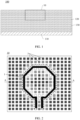
- FIG. 2 is a top view of the inductor device wiring architecture 10 shown in FIG. 1 according to a first embodiment
- FIG. 3 is a schematic cross-sectional view of a partial structure of the inductor device wiring architecture 10 shown in FIG. 2 that is cut along a line A-A.
- a quantity of dummy metals 3 in each metal layer 2 in FIG. 3 is slightly reduced, but an overall arrangement rule remains unchanged.
- the inductor device wiring architecture 10 includes an inductor device 1 and a plurality of dummy metals 3 located under the inductor device 1.
- "under” is merely a direction shown with reference to the accompanying drawings. Therefore, a directional term is used for describing and understanding this application, but not to indicate or imply that an indicated apparatus or element shall have a specific direction or be constructed and operated in a specific direction, and therefore cannot be construed as a limitation on this application.
- the inductor device 1 may be arranged in a top metal layer 120 of the integrated circuit 100.
- a space under the inductor device 1 is a space on a side, of the inductor device 1, that faces the substrate 110 of the integrated circuit 100.
- a structure or a component located under the inductor device 1 is located between the inductor device 1 and the substrate 110.
- the space under the inductor device 1 includes a space under a wiring region of the inductor device 1 (as indicated by a dashed-line box on a periphery of the inductor device 1 in FIG. 2 ).
- the space under the inductor device 1 includes a space in which the wiring region of the inductor device 1 is projected along a vertical direction of a plane on which the inductor device 1 is located.
- the wiring region of the inductor device 1 covers the entire inductor device 1.
- the wiring region of the inductor device 1 includes at least a region surrounded by an outer edge of an outermost wire of the inductor device 1.
- the "vertical direction” described above is not limited to a direction that has an included angle of exactly 90° with the plane on which the inductor device 1 is located, but may be alternatively a direction close to 90°.
- the plurality of dummy metals 3 under the inductor device 1 are located in the space under the inductor device 1.
- the inductor device wiring architecture 10 includes a plurality of laminated metal layers 2.
- the metal layers 2 are some of the corresponding metal layers 120 of the integrated circuit 100.
- the plurality of dummy metals 3 under the inductor device 1 are arranged in a plurality of metal layers 2 under the inductor device 1.
- Each of the plurality of metal layers 2 under the inductor device 1 includes a plurality of corresponding dummy metals 3, to increase a metal arrangement area of the metal layer 2.
- the plurality of metal layers 2 under the inductor device 1 are a bottom structure of the inductor device 1.
- the plurality of dummy metals 3 corresponding to the metal layer 2 under the inductor device 1 are spaced from each other.
- two or more dummy metals 3 may be alternatively combined into a continuous dummy metal with a larger area.
- a plurality of discontinuous dummy metals 3 in the embodiment shown in FIG. 2 may be combined into a continuous dummy metal.
- Dummy metals 3 located in two adjacent metal layers 2 may be connected by using a conductive material in a via, or may not be connected.
- the inductor device 1 is located in a first metal layer 21. Because the inductor device 1 is disposed in the first metal layer 21, the first metal layer 21 can be processed to obtain a larger thickness, thereby reducing a resistance and increasing a quality factor Q.
- a second metal layer 22 to a fifth metal layer 25 are arranged under the inductor device 1.
- the second metal layer 22 to the fifth metal layer 25 are a bottom structure of the inductor device 1.
- the plurality of dummy metals 3 under the inductor device 1 are arranged in the second metal layer 22, the third metal layer 23, the fourth metal layer 24, and the fifth metal layer 25.
- the inductor device wiring architecture 10 further includes a plurality of dummy metals 3 arranged in a metal layer 2 in which the inductor device 1 is located.
- the first metal layer 21 further includes a plurality of dummy metals 3, and the plurality of dummy metals 3 are disposed around the inductor device 1 and are disposed away from the inductor device 1.
- a dummy metal 3 may also be arranged in the middle space.
- Arrangement areas of dummy metals corresponding to at least two metal layers 2 located under the inductor device 1 progressively increase in a direction away from the inductor device 1 (for example, a Z direction shown in FIG. 3 ).
- An arrangement area of dummy metals corresponding to a metal layer 2 is a total arrangement area of dummy metals 3 that are in the metal layer 2 and that are located under the inductor device 1.
- a metal layer 2 with a larger arrangement area of dummy metals 3 has a larger metal arrangement proportion.
- each metal layer 2 of the inductor device wiring architecture 10 has a relatively sufficient metal arrangement area to meet a processing requirement of chemical mechanical polishing, so that the first metal layer 21 is well flattened, and the inductor device 1 has a few metal residues and high processing quality. Therefore, a short circuit risk of a circuit is reduced, and a product yield of the inductor device wiring architecture 10 and the integrated circuit 100 in which the inductor device wiring architecture 10 is used is higher. In short, in the inductor device wiring architecture 10, a metal arrangement area of each metal layer 2 can be increased while adverse effects of the dummy metals 3 on inductor device performance of the inductor device 1 are reduced. This increases a product yield.
- the plurality of dummy metals 3 located under the inductor device 1 are arranged in a stepped shape.
- a dummy metal 3 corresponding to a lower metal layer 2 extends out relative to a dummy metal 3 corresponding to an upper metal layer 2 to form a stepped shape.
- a dummy metal 3 corresponding to the third metal layer 23 extends out relative to a dummy metal 3 corresponding to the second metal layer 22 to form a stepped shape.
- dummy metals 3 located in different metal layers 2 in the inductor device wiring architecture 10 are filled with different patterns for differentiation.
- the inductor device 1 and the dummy metal 3 in the first metal layer 21 are filled with a black pattern
- the dummy metal 3 in the second metal layer 22 is filled with slashes
- the dummy metal 3 in the third metal layer 23 is not filled with a pattern (that is, has a white background color).
- the dummy metals 3 in the plurality of metal layers 2 are arranged in alignment. In this case, a dummy metal 3 in a bottom structure is blocked by a dummy metal 3 in a top structure.
- some dummy metals 3 in the second metal layer 22 are blocked by dummy metals 3 in the first metal layer 21.
- Some dummy metals 3 in the second metal layer 22 extend out relative to dummy metals 3 in the first metal layer 21, and the dummy metals 3 that relatively extend out are exposed.
- the plurality of dummy metals 3 located under the inductor device 1 are arranged in the stepped shape, the plurality of dummy metals 3 can effectively improve metal arrangement under the inductor device 1, so that higher manufacturing precision of the inductor device 1 is high during chemical mechanical polishing, and a product yield of the inductor device wiring architecture 10 and the integrated circuit 100 in which the inductor device wiring architecture 10 is used is higher.
- the plurality of dummy metals 3 located under the inductor device 1 can be arranged not in a region close to the inductor device 1, but arranged in a region away from the inductor device 1 as far as possible, thereby reducing adverse effects of the dummy metals 3 on inductor device performance of the inductor device 1, and improving performance of the inductor device 1.
- Some dummy metals 3 arranged in the metal layer 2 in which the inductor device 1 is located and the dummy metals 3 arranged under the inductor device 1 may also be arranged in a stepped shape.
- a dummy metal 3 corresponding to the second metal layer 22 extends out relative to a dummy metal 3 corresponding to the first metal layer 21 to form a stepped shape.
- some of the plurality of dummy metals 3 in the first metal layer 21 are disposed around the inductor device 1, and some of the plurality of dummy metals 3 in the first metal layer 21 are arranged in the middle space surrounded by the inductor device 1.
- a spacing S1 is formed between the inductor device 1 and a dummy metal 3 closest to the inductor device 1 among the dummy metals 3 located in the middle space of the inductor device 1.
- a spacing S2 is formed between two adjacent dummy metals 3 located in the middle space of the inductor device 1. S1 is greater than S2.
- the dummy metals 3 in the first metal layer 21 have smaller impact on performance of the inductor device 1, and the inductor device 1 has higher inductance performance.
- a spacing between the inductor device 1 and some dummy metals 3 located on a periphery of the inductor device 1 is greater than a spacing between two adjacent dummy metals 3 located on the periphery of the inductor device 1.
- the plurality of dummy metals 3 in the first metal layer 21 may be arranged at equal spacings or unequal spacings. This is not strictly limited in this application.
- a "spacing" between two adjacent dummy metals 3 is a spacing between two dummy metals 3 located on a same side of the inductor device 1.
- the dummy metals 3 in the first metal layer 21 are arranged roughly in an array (no dummy metal 3 is arranged in some regions of the array), and spacings between every two adjacent dummy metals 3 are roughly the same.
- the dummy metals 3 in the first metal layer 21 may be alternatively arranged in another manner, for example, arranged roughly in a diffused annular shape or randomly arranged in a scattered manner.
- a plurality of dummy metals 3 corresponding to the second metal layer 22 are kept away from the inductor device 1 as far as possible.
- a dummy metal 3 in the second metal layer 22 is arranged not directly under a wire of the inductor device 1, to increase a metal arrangement area of the second metal layer 22 as much as possible, so that a product yield of the inductor device wiring architecture 10 is increased, and there is less impact on performance of the inductor device 1.
- a spacing S4 between two dummy metals 3 close to a space directly under a wire of the inductor device 1 is greater than or equal to a gap S5 between two adjacent dummy metals 3.
- some dummy metals 3 corresponding to the second metal layer 22 extend out relative to dummy metals 3 in the first metal layer 21, and a plurality of dummy metals 3 that are in the first metal layer 21 and the second metal layer 22 and that are close to the inductor device 1 are arranged roughly in a stepped shape.
- designs of a structure and a size of the dummy metal 3 in the second metal layer 22 refer to the dummy metal 3 in the first metal layer 21.
- S5 is equal to S2.
- designs of a structure and a size of the dummy metal 3 in the second metal layer 22 may be alternatively different from those of the dummy metal in the first metal layer 21.
- S1 may range from 1 micron ( ⁇ m) to 15 microns. S1 may be set based on a range of an electromagnetic field generated by the inductor device 1.
- S2 may range from 0.1 micron to 10 microns.
- a width of the wire of the inductor device 1 is W1.
- W1 may range from 1 micron to 20 microns.
- a width of the dummy metal 3 is W2.
- W2 may range from 0.1 micron to 10 microns.
- T1 may range from 0.1 micron to 4 microns.
- a copper or aluminum material may be used for the dummy metal 3.
- a copper or aluminum material may be used for the inductor device 1.
- a material of the inductor device 1 is the same as a material of the dummy metal 3 in the first metal layer 21.
- An arrangement area of dummy metals 3 corresponding to the third metal layer 23 is larger than an arrangement area of the dummy metals 3 corresponding to the second metal layer 22. Some dummy metals 3 corresponding to the third metal layer 23 extend out relative to dummy metals 3 corresponding to the second metal layer 22. In this embodiment, a plurality of dummy metals 3 in the first metal layer 21, the second metal layer 22, and the third metal layer 23 are arranged in a stepped shape.
- a dummy metal 3 in the third metal layer 23 is located directly under a wire of the inductor device 1, and a spacing between the dummy metal 3 and the wire of the inductor device 1 is S3.
- S3 may range from 1 micron to 15 microns.
- S3 may be designed based on a range of an electromagnetic field of the inductor device 1.
- designs of a structure and a size of the dummy metal 3 in the third metal layer 23 refer to the dummy metal 3 in the first metal layer 21.
- designs of a structure and a size of the dummy metal 3 in the third metal layer 23 may be alternatively different from those of the dummy metal in the first metal layer 21.
- the inductor device wiring architecture 10 further includes a plurality of dielectric layers 4.
- the dielectric layers 4 are a part of the corresponding insulation layers 130.
- a dielectric layer 4 is disposed between every two adjacent metal layers 2. When a gap is formed between dummy metals 3 in a metal layer 2, the gap is filled with an insulation material to form an insulation part. The insulation part is connected to the dielectric layer 4.
- the dielectric layers 4 in the inductor device wiring architecture 10 may have a same thickness.
- the thickness of the dielectric layer 4 is T2.
- T2 may range from 0.1 micron to 4 microns.
- the plurality of dummy metals 3 under the inductor device 1 are mainly arranged in a stepped shape.
- the plurality of dummy metals 3 under the inductor device 1 may be alternatively arranged in another manner.
- the plurality of dummy metals 3 under the inductor device 1 have a roughly same shape and size.
- the plurality of dummy metals 3 under the inductor device 1 may alternatively have different shapes and different sizes.
- a plurality of dummy metals 3 disposed in a same layer as that of the inductor device 1 and the plurality of dummy metals 3 under the inductor device 1 may have a roughly same shape and size, or may have different shapes and different sizes.
- the plurality of dummy metals 3 under the inductor device 1 are in a square shape.
- the plurality of dummy metals 3 under the inductor device 1 may be alternatively in a strip shape, a triangular shape, a circular shape, an elliptical shape, a polygonal shape, a special shape, or the like.
- a shape and a size of the dummy metal 3 are not strictly limited in this application.
- the inductor device wiring architecture 10 further includes a polycrystalline silicon (polycrystalline silicon) layer (not shown in the figure) located under the plurality of metal layers 2.
- the polycrystalline silicon layer includes a plurality of polycrystalline silicons that serve as gates of PN junctions (a P-type semiconductor and an N-type semiconductor are fabricated on one semiconductor substrate, and a space charge region referred to as a PN junction (PN junction), is formed at a junction interface of the semiconductors) of the integrated circuit 100.
- An arrangement of the plurality of polycrystalline silicons also needs to meet a processing requirement of chemical mechanical polishing to flatten the plurality of metal layers 2.
- For an arrangement rule of the plurality of polycrystalline silicons refer to the foregoing arrangement rule of the plurality of dummy metals 3.
- the polycrystalline silicons in the polycrystalline silicon layer tend to be arranged away from the inductor device 1.
- an arrangement area of the polycrystalline silicons in the polycrystalline silicon layer and the arrangement area of the dummy metals 3 corresponding to the metal layers 2 under the inductor device 1 progressively increase in a direction away from the inductor device 1.
- the plurality of polycrystalline silicons and the plurality of dummy metals 3 located under the inductor device 1 may be jointly arranged in a stepped shape.
- each metal layer 2 corresponds to a plurality of dummy metals 3, and dummy metals 3 corresponding to each metal layer 2 are arranged in a staggered manner with dummy metals 3 corresponding to an adjacent metal layer 2.
- a dummy metal 3 under the inductor device 1 and a dummy metal 3 located above or under the dummy metal 3 have a location relationship of being roughly staggered with each other.
- the plurality of dummy metals 3 located under the inductor device 1 are arranged more regularly, thereby helping reduce design costs and production costs.
- each metal layer 2 corresponds to a plurality of dummy metals 3, and dummy metals 3 corresponding to each metal layer 2 are arranged in alignment with dummy metals 3 corresponding to an adjacent metal layer 2.
- a dummy metal 3 under the inductor device 1 and a dummy metal 3 above or under the dummy metal 3 have a location relationship of roughly facing each other.
- the plurality of dummy metals 3 located under the inductor device 1 are arranged more regularly, thereby helping reduce design costs and production costs.
- each metal layer 2 corresponds to a plurality of dummy metals 3, dummy metals 3 corresponding to one or more metal layers 2 are arranged in a staggered manner with dummy metals 3 corresponding to an adjacent metal layer 2, and dummy metals 3 corresponding to one or more metal layers 2 are arranged in alignment with dummy metals 3 corresponding to an adjacent metal layer 2.
- some dummy metals 3 are arranged in alignment, and some dummy metals 3 are arranged in a staggered manner. This enriches arrangement manners of the dummy metals 3, and makes arrangement manners of the inductor device wiring architecture 10 more diversified.
- dummy metals 3 corresponding to each metal layer 2 are arranged in alignment with dummy metals 3 corresponding to an adjacent metal layer 2.
- dummy metals 3 corresponding to the second metal layer 22 to the fifth metal layer 25 are arranged in alignment.
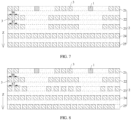
- FIG. 4 is a top view of the inductor device wiring architecture 10 shown in FIG. 1 according to a second embodiment
- FIG. 5 is a schematic cross-sectional view of a partial structure of the inductor device wiring architecture 10 shown in FIG. 4 that is cut along a line B-B.
- a quantity of dummy metals 3 in each metal layer 2 in FIG. 5 is slightly reduced, but an overall arrangement rule remains unchanged.
- Most technical content in this embodiment is the same as that in the foregoing embodiments, and is not described in detail again.
- dummy metals 3 corresponding to each metal layer 2 are arranged in a staggered manner with dummy metals 3 corresponding to an adjacent metal layer 2.
- a layer structure under the inductor device 1 has a more uniform metal arrangement area, thereby helping improve processing precision of the inductor device 1, and achieving a higher product yield of the inductor device wiring architecture 10.
- the inductor device wiring architecture 10 includes a first metal layer 21, a second metal layer 22, a third metal layer 23, a fourth metal layer 24, and a fifth metal layer 25.
- Dummy metals 3 corresponding to the second metal layer 22, the third metal layer 23, the fourth metal layer 24, and the fifth metal layer 25 under the inductor device 1 are arranged in a staggered manner.
- Some dummy metals 3 in the first metal layer 21 in which the inductor device 1 is located are arranged in a staggered manner with the dummy metals 3 corresponding to the metal layers (22, 23, 24, and 25) under the inductor device 1.
- FIG. 6 is a schematic diagram of a partial structure of the inductor device wiring architecture 10 shown in FIG. 1 according to a third embodiment. Most technical content in this embodiment is the same as that in the foregoing embodiments, and is not described in detail again.
- the inductor device wiring architecture 10 includes a first metal layer 21 in which the inductor device 1 is located and a plurality of metal layers (a second metal layer 22 to a ninth metal layer 29) located under the inductor device 1. Arrangement areas of dummy metals 3 corresponding to the second metal layer 22 to the sixth metal layer 26 progressively increase in a Z direction away from the inductor device 1.
- dummy metals 3 corresponding to one or more metal layers 2 are arranged in a staggered manner with dummy metals 3 corresponding to an adjacent metal layer 2, and dummy metals 3 corresponding to one or more metal layers 2 are arranged in alignment with dummy metals 3 corresponding to an adjacent metal layer 2.
- dummy metals 3 corresponding to the second metal layer 22, dummy metals 3 corresponding to the third metal layer 23, and dummy metals 3 corresponding to the fourth metal layer 24 are arranged in alignment.
- the fifth metal layer 25, the sixth metal layer 26, the seventh metal layer 27, the eighth metal layer 28, and the ninth metal layer 29, dummy metals 3 corresponding to two adjacent metal layers 2 are arranged in a staggered manner.
- the plurality of dummy metals 3 located under the inductor device 1 in the inductor device wiring architecture 10 are arranged in a more diversified manner.
- Some dummy metals 3 in the first metal layer 21 are arranged in a staggered manner with dummy metals 3 corresponding to the second metal layer 22. In another embodiment, some dummy metals 3 in the first metal layer 21 are arranged in alignment with dummy metals 3 corresponding to the second metal layer 22.
- An arrangement manner of the dummy metals 3 in the plurality of metal layers 2 in the inductor device wiring architecture 10 is not strictly limited in this application.
- arrangement areas of dummy metals 3 corresponding to at least three adjacent metal layers 2 progressively increase in the Z direction away from the inductor device 1.
- the plurality of dummy metals 3 under the inductor device 1 present a continuous stepped shape. This helps further improve processing quality of the inductor device wiring architecture 10, and the plurality of dummy metals 3 under the inductor device 1 have less impact on performance of the inductor device 1.
- an arrangement area of dummy metals 3 corresponding to an i th metal layer under the inductor device 1 is the same as an arrangement area of dummy metals 3 corresponding to an (i - 1) th metal layer.
- the i th metal layer is located on a side, of the (i - 1) th metal layer, that is away from the inductor device 1. In other words, the i th metal layer is located under the (i - 1) th metal layer.
- i is an integer greater than or equal to 2.
- the inductor device wiring architecture 10 when the inductor device wiring architecture 10 roughly meets an arrangement rule of transitioning from a sparse arrangement to a dense arrangement, two metal layers 2 corresponding to dummy metals 3 with a same arrangement area are included under the inductor device 1, so that arrangement flexibility of the plurality of dummy metals 3 under the inductor device 1 in the inductor device wiring architecture 10 is higher, and arrangement manners are more diversified.
- the inductor device wiring architecture 10 may include one group of two metal layers 2 corresponding to dummy metals 3 with a same arrangement area, or may include more than two (including two) groups of two metal layers 2 corresponding to dummy metals 3 with a same arrangement area. Alternatively, the inductor device wiring architecture 10 may include more than three (including three) metal layers 2 corresponding to dummy metals 3 with a same arrangement area.
- a plurality of dummy metals 3 corresponding to the i th metal layer are arranged at equal spacings, and an arrangement spacing between two adjacent dummy metals 3 is an i th spacing.
- a plurality of dummy metals 3 corresponding to the (i - 1) th metal layer are arranged at equal spacings, and an arrangement spacing between two adjacent dummy metals 3 is an (i - 1) th spacing.
- the (i - 1) th spacing is less than or equal to the i th spacing.
- an arrangement manner and an arrangement spacing of the plurality of dummy metals 3 corresponding to the i th metal layer and the (i - 1) th metal layer may be alternatively different from those in the foregoing solution, and may be set as required.
- an arrangement area of dummy metals 3 corresponding to a j th metal layer under the inductor device 1 is smaller than an arrangement area of dummy metals 3 corresponding to a (j - 1) th metal layer.
- the j th metal layer is located on a side, of the (j - 1) th metal layer, that is away from the inductor device 1. In other words, the j th metal layer is located under the (j - 1) th metal layer.
- j is an integer greater than or equal to 2.
- the inductor device wiring architecture 10 when the inductor device wiring architecture 10 roughly meets an arrangement rule of transitioning from a sparse arrangement to a dense arrangement, two metal layers 2 corresponding to dummy metals 3 are included under the inductor device 1, where an arrangement area of an upper metal layer is smaller than an arrangement area of a lower metal layer, so that arrangement flexibility of the plurality of dummy metals 3 under the inductor device 1 in the inductor device wiring architecture 10 is higher, and arrangement manners are more diversified.
- the inductor device wiring architecture 10 may include one group of two metal layers 2 corresponding to dummy metals 3, or may include more than two (including two) groups of two metal layers 2 corresponding to dummy metals 3, where an arrangement area of an upper metal layer is smaller than an arrangement area of a lower metal layer.
- the inductor device wiring architecture 10 may include more than three (including three) metal layers 2 corresponding to dummy metals 3, where an arrangement area of an upper metal layer is smaller than an arrangement area of a lower metal layer.
- a plurality of dummy metals 3 corresponding to the j th metal layer are arranged at equal spacings, and an arrangement spacing between two adjacent dummy metals 3 is a j th spacing.
- a plurality of dummy metals 3 corresponding to the (j - 1) th metal layer are arranged at equal spacings, and an arrangement spacing between two adjacent dummy metals 3 is a (j - 1) th spacing.
- the (j - 1) th spacing is less than or equal to the j th spacing.
- an arrangement manner and an arrangement spacing of the plurality of dummy metals 3 corresponding to the j th metal layer and the (j - 1) th metal layer may be alternatively different from those in the foregoing solution, and may be set as required.
- an arrangement area of dummy metals 3 corresponding to at least two of the plurality of metal layers 2 under the inductor device 1 progressively increase in the direction away from the inductor device 1
- an arrangement area of dummy metals 3 corresponding to one or more metal layers 2 and an arrangement area of dummy metals 3 corresponding to an adjacent metal layer 2 may be the same or progressively decrease (in the Z direction away from the inductor device 1).
- a higher product yield can also be achieved for the inductor device wiring architecture 10.
- the inductor device 1 is arranged in the first metal layer 21. Arrangement areas of dummy metals 3 corresponding to the second metal layer 22 and the third metal layer 23 under the inductor device 1 progressively increase in the direction away from the inductor device 1.
- An arrangement area of dummy metals 3 corresponding to the fourth metal layer 24 (that is, a 3 rd metal layer under the inductor device 1) is the same as an arrangement area of dummy metals 3 corresponding to the third metal layer 23 (that is, a 2 nd metal layer under the inductor device 1).
- An arrangement area of dummy metals 3 corresponding to the fifth metal layer 25 (that is, a 4 th metal layer under the inductor device 1) is the same as the arrangement area of the dummy metals 3 corresponding to the fourth metal layer 24 (that is, the 3 rd metal layer under the inductor device 1).
- an arrangement area of dummy metals 3 corresponding to an i th metal layer under the inductor device 1 is the same as an arrangement area of dummy metals 3 corresponding to an (i - 1) th metal layer.
- the i th metal layer is located on a side, of the (i - 1) th metal layer, that is away from the inductor device 1.
- i is an integer greater than or equal to 2.
- a plurality of dummy metals 3 corresponding to the fourth metal layer 24 (that is, the 3 rd metal layer under the inductor device 1) are arranged at equal spacings, and an arrangement spacing between two adjacent dummy metals 3 is a third spacing.
- a plurality of dummy metals 3 corresponding to the third metal layer 23 (that is, the 2 nd metal layer under the inductor device 1) are arranged at equal spacings, and an arrangement spacing between two adjacent dummy metals 3 is a second spacing. The second spacing is equal to the third spacing.
- a plurality of dummy metals 3 corresponding to the fifth metal layer 25 (that is, the 4 th metal layer under the inductor device 1) are arranged at equal spacings, and an arrangement spacing between two adjacent dummy metals 3 is a fourth spacing.
- the fourth spacing is equal to the third spacing.
- the arrangement area of the dummy metals 3 corresponding to the third metal layer 23 (that is, the 2 nd metal layer under the inductor device 1), the arrangement area of the dummy metals 3 corresponding to the fourth metal layer 24 (that is, the 3 rd metal layer under the inductor device 1), and the arrangement area of the dummy metals 3 corresponding to the fifth metal layer 25 (that is, the 4 th metal layer under the inductor device 1) are the same.
- more than three (including three) metal layers 2 under the inductor device 1 correspond to dummy metals 3 with a same arrangement area.
- the inductor device 1 is arranged in the first metal layer 21.
- the second metal layer 22 is disposed adjacent to the third metal layer 23 and the fourth metal layer 24 under the inductor device 1.
- arrangement areas of dummy metals 3 corresponding to the second metal layer 22, the third metal layer 23, and the fourth metal layer 24 progressively increase in the Z direction away from the inductor device 1.
- arrangement areas of dummy metals 3 corresponding to at least three adjacent metal layers 2 progressively increase in the Z direction away from the inductor device 1.
- An arrangement area of dummy metals 3 corresponding to the fifth metal layer 25 (that is, a 4 th metal layer under the inductor device 1) is smaller than an arrangement area of dummy metals 3 corresponding to the fourth metal layer 24 (that is, a 3 rd metal layer under the inductor device 1).
- a plurality of dummy metals 3 corresponding to the fifth metal layer 25 (that is, the 4 th metal layer under the inductor device 1) are arranged at equal spacings, and an arrangement spacing between two adjacent dummy metals 3 is a fourth spacing.
- a plurality of dummy metals 3 corresponding to the fourth metal layer 24 (that is, the 3 rd metal layer under the inductor device 1) are arranged at equal spacings, and an arrangement spacing between two adjacent dummy metals 3 is a third spacing.
- the third spacing is equal to the fourth spacing.
- the inductor device 1 is arranged in the first metal layer 21.
- the second metal layer 22 is disposed adjacent to the third metal layer 23, the fourth metal layer 24, the fifth metal layer 25, and the sixth metal layer 26 under the inductor device 1.
- arrangement areas of dummy metals 3 corresponding to the second metal layer 22 to the sixth metal layer 26 progressively increase in the direction away from the inductor device 1.
- Arrangement areas of dummy metals 3 corresponding to the sixth metal layer 26 that is, a 5 th metal layer under the inductor device 1), the seventh metal layer 27 (that is, a 6 th metal layer under the inductor device 1), the eighth metal layer 28 (that is, a 7 th metal layer under the inductor device 1), and the ninth metal layer 29 (that is, an 8 th metal layer under the inductor device 1) are the same.
- more than three (including three) metal layers 2 under the inductor device 1 correspond to dummy metals 3 with a same arrangement area.
- each metal layer 2 corresponds to a plurality of dummy metals 3, and an arrangement spacing between two adjacent dummy metals 3 remains the same in different metal layers 2.
- an arrangement spacing between two adjacent dummy metals 3 may alternatively vary in different metal layers 2.
- FIG. 7 is a schematic structural diagram of the inductor device wiring architecture 10 shown in FIG. 1 according to a fourth embodiment. Most technical content in this embodiment is the same as that in the foregoing embodiments, and is not described in detail again.
- the inductor device 1 is arranged in a first metal layer 21. Arrangement areas of dummy metals 3 corresponding to a third metal layer 23 and a fourth metal layer 24 under the inductor device 1 progressively increase in a Z direction away from the inductor device 1.
- a second metal layer 22 and the fourth metal layer 24 are spaced from each other. Arrangement areas of dummy metals 3 corresponding to the second metal layer 22 and the fourth metal layer 24 progressively increase in the Z direction away from the inductor device 1.
- An arrangement area of dummy metals 3 corresponding to the third metal layer 23 (that is, a 2 nd metal layer under the inductor device 1) is the same as an arrangement area of dummy metals 3 corresponding to the second metal layer 22 (that is, a 1 st metal layer under the inductor device 1).
- An arrangement area of dummy metals 3 corresponding to a fifth metal layer 25 (that is, a 4 th metal layer under the inductor device 1) is the same as an arrangement area of dummy metals 3 corresponding to the fourth metal layer 24 (that is, a 3 rd metal layer under the inductor device 1).
- two or more groups of two metal layers 2 corresponding to dummy metals 3 with a same arrangement area may be included under the inductor device 1.
- An arrangement spacing between two adjacent dummy metals 3 in a plurality of dummy metals 3 corresponding to the third metal layer 23 (that is, the 2 nd metal layer under the inductor device 1) is a second spacing S7.
- An arrangement spacing between two adjacent dummy metals 3 in a plurality of dummy metals 3 corresponding to the second metal layer 22 (that is, the 1 st metal layer under the inductor device 1) is a first spacing S6.
- the first spacing S6 is equal to the second spacing S7.
- An arrangement spacing between two adjacent dummy metals 3 in a plurality of dummy metals 3 corresponding to the fifth metal layer 25 (that is, the 4 th metal layer under the inductor device 1) is a fourth spacing.
- An arrangement spacing between two adjacent dummy metals 3 in a plurality of dummy metals 3 corresponding to the fourth metal layer 24 (that is, the 3 rd metal layer under the inductor device 1) is a third spacing.
- the third spacing is equal to the fourth spacing.
- the third spacing may be equal to or not equal to the second spacing.
- FIG. 8 is a schematic structural diagram of the inductor device wiring architecture 10 shown in FIG. 1 according to a fifth embodiment. Most technical content in this embodiment is the same as that in the foregoing embodiments, and is not described in detail again.
- the inductor device 1 is arranged in a first metal layer 21. Arrangement areas of dummy metals 3 corresponding to a third metal layer 23 and a fourth metal layer 24 under the inductor device 1 progressively increase in a Z direction away from the inductor device 1.
- An arrangement area of dummy metals 3 corresponding to the third metal layer 23 (that is, a 2 nd metal layer under the inductor device 1) is the same as an arrangement area of dummy metals 3 corresponding to the second metal layer 22 (that is, a 1 st metal layer under the inductor device 1).
- An arrangement spacing between two adjacent dummy metals 3 in a plurality of dummy metals 3 corresponding to the third metal layer 23 is a second spacing S7.
- An arrangement spacing between two adjacent dummy metals 3 in a plurality of dummy metals 3 corresponding to the second metal layer 22 is a first spacing S6.
- the first spacing S6 is less than the second spacing S7.
- An arrangement area of dummy metals 3 corresponding to the fifth metal layer 25 (that is, a 4 th metal layer under the inductor device 1) is smaller than an arrangement area of dummy metals 3 corresponding to the fourth metal layer 24 (that is, a 3 rd metal layer under the inductor device 1).
- a plurality of dummy metals 3 in a plurality of dummy metals 3 corresponding to the fifth metal layer 25 (that is, the 4 th metal layer under the inductor device 1) are arranged at equal spacings, and an arrangement spacing between two adjacent dummy metals 3 is a fourth spacing.
- a plurality of dummy metals 3 corresponding to the fourth metal layer 24 (that is, the 3 rd metal layer under the inductor device 1) are arranged at equal spacings, and an arrangement spacing between two adjacent dummy metals 3 is a third spacing.
- the third spacing is equal to the fourth spacing.
- FIG. 9 is a schematic diagram of a partial structure of the inductor device wiring architecture 10 shown in FIG. 1 according to a sixth embodiment. Most technical content in this embodiment is the same as that in the foregoing embodiments, and is not described in detail again.
- the inductor device 1 is arranged in a first metal layer 21. Arrangement areas of dummy metals 3 corresponding to a second metal layer 22 and a third metal layer 23 under the inductor device 1 progressively increase in a direction away from the inductor device 1. Arrangement areas of dummy metals 3 corresponding to a fourth metal layer 24, a fifth metal layer 25, and a sixth metal layer 26 progressively increase in the direction away from the inductor device 1.
- An arrangement area of dummy metals 3 corresponding to the fourth metal layer 24 (that is, a 3 rd metal layer under the inductor device 1) is the same as an arrangement area of dummy metals 3 corresponding to the third metal layer 23 (that is, a 2 nd metal layer under the inductor device 1).
- Arrangement areas of dummy metals 3 corresponding to the sixth metal layer 26 (that is, a 5 th metal layer under the inductor device 1), a seventh metal layer 27 (that is, a 6 th metal layer under the inductor device 1), an eighth metal layer 28 (that is, a 7 th metal layer under the inductor device 1), and a ninth metal layer 29 (that is, an 8 th metal layer under the inductor device 1) are the same.
- FIG. 10 is a schematic structural diagram of the inductor device wiring architecture 10 shown in FIG. 1 according to a seventh embodiment. Most technical content in this embodiment is the same as that in the foregoing embodiments, and is not described in detail again.
- the inductor device 1 is arranged in a first metal layer 21. Arrangement areas of dummy metals 3 corresponding to a third metal layer 23 and a fourth metal layer 24 under the inductor device 1 progressively increase in a direction away from the inductor device 1.
- An arrangement area of dummy metals 3 corresponding to the third metal layer 23 (that is, a 2 nd metal layer under the inductor device 1) is smaller than an arrangement area of dummy metals 3 corresponding to a second metal layer 22 (that is, a 1 st metal layer under the inductor device 1).
- An arrangement spacing between two adjacent dummy metals 3 in a plurality of dummy metals 3 corresponding to the third metal layer 23 is a second spacing S7.
- An arrangement spacing between two adjacent dummy metals 3 in a plurality of dummy metals 3 corresponding to the second metal layer 22 is a first spacing S6.
- the first spacing S6 is equal to the second spacing S7.
- An arrangement area of dummy metals 3 corresponding to a fifth metal layer 25 (that is, a 4 th metal layer under the inductor device 1) is the same as an arrangement area of dummy metals 3 corresponding to the fourth metal layer 24 (that is, a 3 rd metal layer under the inductor device 1).
- An arrangement spacing between two adjacent dummy metals 3 in a plurality of dummy metals 3 corresponding to the fifth metal layer 25 (that is, the 4 th metal layer under the inductor device 1) is equal to an arrangement spacing between two adjacent dummy metals 3 in a plurality of dummy metals 3 corresponding to the fourth metal layer 24 (that is, the 3 rd metal layer under the inductor device 1).
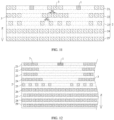
- FIG. 11 is a schematic structural diagram of the inductor device wiring architecture 10 shown in FIG. 1 according to an eighth embodiment. Most technical content in this embodiment is the same as that in the foregoing embodiments, and is not described in detail again.
- the inductor device 1 is arranged in a first metal layer 21. Arrangement areas of dummy metals 3 corresponding to a third metal layer 23 and a fourth metal layer 24 under the inductor device 1 progressively increase in a direction away from the inductor device 1.
- An arrangement area of dummy metals 3 corresponding to the third metal layer 23 (that is, a 2 nd metal layer under the inductor device 1) is smaller than an arrangement area of dummy metals 3 corresponding to a second metal layer 22 (that is, a 1 st metal layer under the inductor device 1).
- An arrangement spacing between two adjacent dummy metals 3 in a plurality of dummy metals 3 corresponding to the third metal layer 23 (that is, the 2 nd metal layer under the inductor device 1) is a second spacing S7.
- An arrangement spacing between two adjacent dummy metals 3 in a plurality of dummy metals 3 corresponding to the second metal layer 22 (that is, the 1 st metal layer under the inductor device 1) is a first spacing S6.
- the first spacing S6 is less than the second spacing S7.
- An arrangement area of dummy metals 3 corresponding to a fifth metal layer 25 (that is, a 4 th metal layer under the inductor device 1) is the same as an arrangement area of dummy metals 3 corresponding to the fourth metal layer 24 (that is, a 3 rd metal layer under the inductor device 1).
- An arrangement spacing between two adjacent dummy metals 3 in a plurality of dummy metals 3 corresponding to the fifth metal layer 25 is equal to an arrangement spacing between two adjacent dummy metals 3 in a plurality of dummy metals 3 corresponding to the fourth metal layer 24 (that is, the 3 rd metal layer under the inductor device 1).
- FIG. 12 is a schematic diagram of a partial structure of the inductor device wiring architecture 10 shown in FIG. 1 according to a ninth embodiment. Most technical content in this embodiment is the same as that in the foregoing embodiments, and is not described in detail again.
- the inductor device 1 is arranged in a first metal layer 21. Arrangement areas of dummy metals 3 corresponding to a third metal layer 23 and a fourth metal layer 24 under the inductor device 1 progressively increase in a direction away from the inductor device 1. Arrangement areas of dummy metals 3 corresponding to a fifth metal layer 25 and a sixth metal layer 26 progressively increase in the direction away from the inductor device 1.
- An arrangement area of dummy metals 3 corresponding to the third metal layer 23 (that is, a 2 nd metal layer under the inductor device 1) is smaller than an arrangement area of dummy metals 3 corresponding to a second metal layer 22 (that is, a 1 st metal layer under the inductor device 1).
- An arrangement area of dummy metals 3 corresponding to the fifth metal layer 25 (that is, a 4 th metal layer under the inductor device 1) is smaller than an arrangement area of dummy metals 3 corresponding to the fourth metal layer 24 (that is, a 3 rd metal layer under the inductor device 1).
- a plurality of dummy metals 3 in a plurality of dummy metals 3 corresponding to the third metal layer 23 are arranged at equal spacings, and an arrangement spacing between two adjacent dummy metals 3 is a second spacing.
- a plurality of dummy metals 3 corresponding to the third metal layer 23 (that is, the 2 nd metal layer under the inductor device 1) are arranged at equal spacings, and an arrangement spacing between two adjacent dummy metals 3 is a first spacing. The first spacing is equal to the second spacing.
- a plurality of dummy metals 3 corresponding to the fifth metal layer 25 (that is, the 4 th metal layer under the inductor device 1) are arranged at equal spacings, and an arrangement spacing between two adjacent dummy metals 3 is a fourth spacing.
- a plurality of dummy metals 3 corresponding to the fourth metal layer 24 (that is, the 3 rd metal layer under the inductor device 1) are arranged at equal spacings, and an arrangement spacing between two adjacent dummy metals 3 is a third spacing. The third spacing is equal to the fourth spacing.
- Arrangement areas of dummy metals 3 corresponding to the sixth metal layer 26 that is, a 5 th metal layer under the inductor device 1), a seventh metal layer 27 (that is, a 6 th metal layer under the inductor device 1), an eighth metal layer 28 (that is, a 7 th metal layer under the inductor device 1), and a ninth metal layer 29 (that is, an 8 th metal layer under the inductor device 1) are the same.
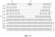
- FIG. 13 is a schematic diagram of a partial structure of the inductor device wiring architecture 10 shown in FIG. 1 according to a tenth embodiment. Most technical content in this embodiment is the same as that in the foregoing embodiments, and is not described in detail again.
- the inductor device 1 is arranged in a first metal layer 21. Arrangement areas of dummy metals 3 corresponding to a second metal layer 22 and a third metal layer 23 under the inductor device 1 progressively increase in a direction away from the inductor device 1.
- a fourth metal layer 24 is disposed adjacent to a fifth metal layer 25, and a sixth metal layer 26. In addition, arrangement areas of dummy metals 3 corresponding to the fourth metal layer 24, the fifth metal layer 25, and the sixth metal layer 26 progressively increase in the direction away from the inductor device 1.
- An arrangement area of dummy metals 3 corresponding to the second metal layer 22 (that is, a 1 st metal layer under the inductor device 1) is the same as an arrangement area of dummy metals 3 corresponding to the first metal layer 21 (that is, a metal layer in which the inductor device 1 is located).
- An arrangement spacing between two adjacent dummy metals in a plurality of dummy metals 3 corresponding to the second metal layer 22 (that is, the 1 st metal layer under the inductor device 1) is greater than an arrangement spacing between two adjacent dummy metals in a plurality of dummy metals 3 corresponding to the first metal layer 21 (that is, the metal layer in which the inductor device 1 is located).
- An arrangement area of dummy metals 3 corresponding to the fourth metal layer 24 (that is, a 3 rd metal layer under the inductor device 1) is smaller than an arrangement area of dummy metals 3 corresponding to the third metal layer 24 (that is, a 2 nd metal layer under the inductor device 1).
- a plurality of dummy metals 3 corresponding to the fourth metal layer 24 (that is, the 3 rd metal layer under the inductor device 1) are arranged at equal spacings, and an arrangement spacing between two adjacent dummy metals 3 is a third spacing.
- a plurality of dummy metals 3 corresponding to the third metal layer 24 (that is, the 2 nd metal layer under the inductor device 1) are arranged at equal spacings, and an arrangement spacing between two adjacent dummy metals 3 is a second spacing. The second spacing is less than the third spacing.
- Arrangement areas of dummy metals 3 corresponding to the sixth metal layer 26 that is, a 5 th metal layer under the inductor device 1), a seventh metal layer 27 (that is, a 6 th metal layer under the inductor device 1), an eighth metal layer 28 (that is, a 7 th metal layer under the inductor device 1), and a ninth metal layer 29 (that is, an 8 th metal layer under the inductor device 1) are the same.
- the first embodiment to the tenth embodiment schematically describe an arrangement relationship of the plurality of dummy metals 3 under the inductor device 1, but do not strictly limit the arrangement relationship of the plurality of dummy metals 3 under the inductor device 1 (for example, a relationship between arrangement spacings in a single metal layer 2 and an arrangement spacing between a plurality of metal layers 2).
- the plurality of dummy metals 3 in the metal layers 2 under the inductor device 1 may be alternatively arranged randomly or according to another arrangement rule.
- the inductor device 1 may have a plurality of implementation structures.
- the inductor device 1 may be an inductor with two ports or a transformer (transformer) with four ports.
- the inductor device 1 may be arranged in one metal layer; or the inductor device 1 may include an upper inductor and a lower inductor, and the upper inductor and the lower inductor are arranged in two adjacent metal layers.
- the inductor device 1 in the inductor device wiring architecture 10 is an inductor with two ports.
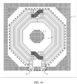
- FIG. 14 shows an implementation structure of the inductor device 1 in the inductor device wiring architecture 10 shown in FIG. 1 .
- FIG. 14 is a top view of a metal layer in which the inductor device 1 of the inductor device wiring architecture 10 is located.
- the inductor device 1 in the inductor device wiring architecture 10 is a helical inductor with two ports.
- the helical inductor is arranged in one metal layer. 180° is formed between the two ports 11 of the helical inductor.
- a main structure of the helical inductor is arranged in one metal layer.
- the metal layer in which the inductor device 1 is located further includes a plurality of dummy metals 3. Some dummy metals 3 are arranged around a periphery of the helical inductor. Some dummy metals 3 are arranged in a middle space surrounded by the helical inductor.
- a wiring region of the inductor device 1 is schematically indicated by a dashed-line box on a periphery of the inductor device 1.
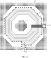
- FIG. 15 shows another implementation structure of the inductor device 1 in the inductor device wiring architecture 10 shown in FIG. 1 .
- FIG. 15 is a top view of a metal layer in which the inductor device 1 of the inductor device wiring architecture 10 is located.
- the inductor device 1 in the inductor device wiring architecture 10 is a helical inductor with two ports. 90° is formed between the two ports 11 of the helical inductor.
- a main structure of the helical inductor is arranged in one metal layer.
- the metal layer in which the inductor device 1 is located further includes a plurality of dummy metals 3. Some dummy metals 3 are arranged around a periphery of the helical inductor. Some dummy metals 3 are arranged in a middle space surrounded by the helical inductor.
- a wiring region of the inductor device 1 is schematically indicated by a dashed-line box on a periphery of the inductor device 1.
- FIG. 16 shows still another implementation structure of the inductor device 1 in the inductor device wiring architecture 10 shown in FIG. 1 .
- FIG. 16 is a top view of a metal layer in which the inductor device 1 of the inductor device wiring architecture 10 is located.
- the inductor device 1 in the inductor device wiring architecture 10 is a differential inductor with two ports.
- a main structure of the differential inductor is arranged in one metal layer.
- the metal layer in which the inductor device 1 is located further includes a plurality of dummy metals 3. Some dummy metals 3 are arranged around a periphery of the differential inductor. Some dummy metals 3 are arranged in a middle space surrounded by the differential inductor.
- a wiring region of the inductor device 1 is schematically indicated by a dashed-line box on a periphery of the inductor device 1.
- FIG. 17 shows still another implementation structure of the inductor device 1 in the inductor device wiring architecture 10 shown in FIG. 1 .
- FIG. 17 is a top view of a metal layer in which the inductor device 1 of the inductor device wiring architecture 10 is located.
- the inductor device 1 in the inductor device wiring architecture 10 is a square inductor with two ports.
- a main structure of the square inductor is arranged in one metal layer.
- the metal layer in which the inductor device 1 is located further includes a plurality of dummy metals 3. Some dummy metals 3 are arranged around a periphery of the square inductor. Some dummy metals 3 are arranged in a middle space surrounded by the square inductor.
- a wiring region of the inductor device 1 is schematically indicated by a dashed-line box on a periphery of the inductor device 1.
- the square inductor is a differential inductor.
- the square inductor may be alternatively another inductor.
- the inductor may alternatively be an inductor in another shape, for example, a circular shape or a polygonal shape. This is not strictly limited in this application.
- FIG. 18 shows still another implementation structure of the inductor device 1 in the inductor device wiring architecture 10 shown in FIG. 1 .
- FIG. 18 is a top view of a metal layer in which the inductor device 1 of the inductor device wiring architecture 10 is located.
- the inductor device 1 in the inductor device wiring architecture 10 is a transformer with four ports.
- the transformer includes two coils that are intertwined. Each coil has two ports 11.
- a main structure of the transformer is arranged in one metal layer.
- the metal layer in which the inductor device 1 is located further includes a plurality of dummy metals 3. Some dummy metals 3 are arranged around a periphery of the transformer. Some dummy metals 3 are arranged in a middle space surrounded by the transformer.
- a wiring region of the inductor device 1 is schematically indicated by a dashed-line box on a periphery of the inductor device 1.
- FIG. 19 shows still another implementation structure of the inductor device 1 in the inductor device wiring architecture 10 shown in FIG. 1 .
- FIG. 19 is a schematic three-dimensional structural diagram of the inductor device 1.
- the inductor device 1 may include an upper inductor 12 and a lower inductor 13.
- the upper inductor 12 and the lower inductor 13 are arranged in two adjacent metal layers.
- the upper inductor 12 and the lower inductor 13 may be connected by using a conductive material 14 in a via, so that the inductor device 1 serves as a multilayer metal serial (serial) inductor.
- the wiring region of the inductor device 1 includes a region surrounded by an outer edge of an outermost wire of the upper inductor 12 and a region surrounded by an outer edge of an outermost wire of the lower inductor 13.
- the plurality of implementation structures of the inductor device 1 are all used in the inductor device wiring architecture 10 shown in the first embodiment to the tenth embodiment.
- the inductor device 1 in the inductor device wiring architecture 10 may be alternatively replaced with another transmission wire to form a transmission wire wiring architecture.
- the transmission wire may be used to transmit a signal with a frequency higher than 100 megahertz.
- the transmission wire may be a key signal wire used to transmit a radio frequency signal.
Landscapes
- Engineering & Computer Science (AREA)
- Power Engineering (AREA)
- Microelectronics & Electronic Packaging (AREA)
- Semiconductor Integrated Circuits (AREA)
- Internal Circuitry In Semiconductor Integrated Circuit Devices (AREA)
Claims (13)
- Verdrahtungsarchitektur (10) einer Induktorvorrichtung, Folgendes umfassend:eine Induktorvorrichtung (1) und eine Vielzahl von Scheinmetallen (dummy metals) (3), die sich unter der Induktorvorrichtung (1) befindet, wobeidie Vielzahl von Scheinmetallen (3) in einer Vielzahl von Metallschichten (2) angeordnet ist, jede der Vielzahl von Metallschichten (2) einigen der Vielzahl von Scheinmetallen (3) entspricht, dadurch gekennzeichnet, dass Anordnungsflächen von Scheinmetallen (3), die mindestens drei benachbarten Metallschichten der Vielzahl von Metallschichten (2) entsprechen, in einer Richtung weg von der Induktorvorrichtung fortschreitend zunehmen.
- Verdrahtungsarchitektur (10) einer Induktorvorrichtung gemäß Anspruch 1, wobei die Vielzahl von Scheinmetallen (3) in einer Stufenform angeordnet ist.
- Verdrahtungsarchitektur (10) einer Induktorvorrichtung gemäß Anspruch 1 oder 2, wobei eine Anordnungsfläche von Scheinmetallen (3), die einer i-ten Metallschicht unter der Induktorvorrichtung entspricht, die gleiche ist wie eine Anordnungsfläche von Scheinmetallen (3), die einer (i - 1)-ten Metallschicht entspricht, die i-te Metallschicht sich auf einer Seite der (i - 1)-ten Metallschicht befindet, die von der Induktorvorrichtung (1) entfernt ist, und i eine ganze Zahl größer oder gleich 2 ist.
- Verdrahtungsarchitektur (10) einer Induktorvorrichtung gemäß Anspruch 3, wobei eine Vielzahl von Scheinmetallen (3), die der i-ten Metallschicht entsprechen, in gleichmäßigen Abständen angeordnet ist und ein Anordnungsabstand zwischen zwei benachbarten Scheinmetallen (3) ein i-ter Abstand ist; eine Vielzahl von Scheinmetallen (3), die der (i - 1)-ten Metallschicht entspricht, in gleichmäßigen Abständen angeordnet ist und ein Anordnungsabstand zwischen zwei benachbarten Scheinmetallen (3) ein (i - 1)-ter Abstand ist; und der (i - 1)-te Abstand kleiner als der i-te Abstand ist.
- Verdrahtungsarchitektur (10) einer Induktorvorrichtung gemäß einem der Ansprüche 1 bis 4, wobei eine Anordnungsfläche von Scheinmetallen (3), die einer j-ten Metallschicht unter der Induktorvorrichtung (1) entspricht, kleiner ist als eine Anordnungsfläche von Scheinmetallen (3), die einer (j - 1)-ten Metallschicht entspricht, die j-te Metallschicht sich auf einer Seite der (j - 1)-ten Metallschicht befindet, die von der Induktorvorrichtung (1) entfernt ist, und j eine ganze Zahl größer oder gleich 2 ist.
- Verdrahtungsarchitektur (10) einer Induktorvorrichtung gemäß Anspruch 5, wobei eine Vielzahl von Scheinmetallen (3), die der j-ten Metallschicht entsprechen, in gleichmäßigen Abständen angeordnet ist und ein Anordnungsabstand zwischen zwei benachbarten Scheinmetallen (3) ein j-ter Abstand ist; eine Vielzahl von Scheinmetallen (3), die der (j - 1)-ten Metallschicht entspricht, in gleichmäßigen Abständen angeordnet ist und ein Anordnungsabstand zwischen zwei benachbarten Scheinmetallen (3) ein (j - 1)-ter Abstand ist; und der (j - 1)-te Abstand kleiner als der j-te Abstand ist.
- Verdrahtungsarchitektur (10) einer Induktorvorrichtung gemäß einem der Ansprüche 1 bis 6, wobei unter der Induktorvorrichtung (1) jede Metallschicht (2) einer Vielzahl von Scheinmetallen (3) entspricht und die Scheinmetalle (3), die der Metallschicht entsprechen, in einer versetzten Weise mit Scheinmetallen (3) angeordnet sind, die einer benachbarten Metallschicht entsprechen.
- Verdrahtungsarchitektur (10) einer Induktorvorrichtung gemäß einem der Ansprüche 1 bis 4 und 6, wobei unter der Induktorvorrichtung (1) jede Metallschicht (2) eine Vielzahl von Scheinmetallen (3) aufweist und die Scheinmetalle (3), die der Metallschicht entsprechen, in Ausrichtung mit Scheinmetallen (3) angeordnet sind, die einer benachbarten Metallschicht entsprechen.
- Verdrahtungsarchitektur (10) einer Induktorvorrichtung gemäß einem der Ansprüche 1 bis 6, wobei unter der Induktorvorrichtung (1) jede Metallschicht (2) einer Vielzahl von Scheinmetallen (3) entspricht, Scheinmetalle (3), die einer oder mehreren Metallschichten (2) entsprechen, in einer versetzten Weise mit Scheinmetallen (3) angeordnet sind, die einer benachbarten Metallschicht entsprechen, und Scheinmetalle (3), die einer oder mehreren Metallschichten (2) entsprechen, in Ausrichtung mit Scheinmetallen (3) angeordnet sind, die einer benachbarten Metallschicht entsprechen.
- Verdrahtungsarchitektur (10) einer Induktorvorrichtung gemäß einem der Ansprüche 1 bis 9, wobei die Induktorvorrichtung (1) ein Induktor mit zwei Anschlüssen oder ein Transformator mit vier Anschlüssen ist.
- Verdrahtungsarchitektur (10) einer Induktorvorrichtung gemäß einem der Ansprüche 1 bis 10, wobei die Induktorvorrichtung (1) in einer Metallschicht angeordnet ist; oder die Induktorvorrichtung einen oberen Induktor und einen unteren Induktor umfasst, und der obere Induktor und der untere Induktor in zwei benachbarten Metallschichten angeordnet sind.
- Integrierte Schaltung (100), umfassend die Verdrahtungsarchitektur (10) einer Induktorvorrichtung gemäß einem der Ansprüche 1 bis 11.
- Kommunikationsvorrichtung, umfassend die integrierte Schaltung (100) gemäß Anspruch 12.
Applications Claiming Priority (1)
| Application Number | Priority Date | Filing Date | Title |
|---|---|---|---|
| PCT/CN2019/080664 WO2020199036A1 (zh) | 2019-03-29 | 2019-03-29 | 电感器件布线架构、集成电路及通信设备 |
Publications (3)
| Publication Number | Publication Date |
|---|---|
| EP3937232A1 EP3937232A1 (de) | 2022-01-12 |
| EP3937232A4 EP3937232A4 (de) | 2022-03-23 |
| EP3937232B1 true EP3937232B1 (de) | 2025-01-22 |
Family
ID=72664470
Family Applications (1)
| Application Number | Title | Priority Date | Filing Date |
|---|---|---|---|
| EP19923130.9A Active EP3937232B1 (de) | 2019-03-29 | 2019-03-29 | Architektur von induktiver verdrahtung, integrierte schaltung und kommunikationsvorrichtung |
Country Status (4)
| Country | Link |
|---|---|
| US (1) | US12354954B2 (de) |
| EP (1) | EP3937232B1 (de) |
| CN (1) | CN113614915B (de) |
| WO (1) | WO2020199036A1 (de) |
Families Citing this family (1)
| Publication number | Priority date | Publication date | Assignee | Title |
|---|---|---|---|---|
| US20240321730A1 (en) * | 2023-03-24 | 2024-09-26 | Qualcomm Incorporated | Integrated device comprising stacked inductors with low or no mutual inductance |
Family Cites Families (15)
| Publication number | Priority date | Publication date | Assignee | Title |
|---|---|---|---|---|
| JP2002110908A (ja) * | 2000-09-28 | 2002-04-12 | Toshiba Corp | スパイラルインダクタおよびこれを備える半導体集積回路装置の製造方法 |
| JP2002373896A (ja) * | 2001-06-15 | 2002-12-26 | Mitsubishi Electric Corp | 半導体装置 |
| TW200802430A (en) * | 2006-01-09 | 2008-01-01 | Koninkl Philips Electronics Nv | Integrated circuit inductor with small floating metal structures |
| JP5180625B2 (ja) * | 2007-03-12 | 2013-04-10 | ルネサスエレクトロニクス株式会社 | 半導体装置 |
| JP5156324B2 (ja) * | 2007-10-10 | 2013-03-06 | ルネサスエレクトロニクス株式会社 | 半導体装置及び半導体装置の製造方法 |
| JP5501668B2 (ja) * | 2009-06-17 | 2014-05-28 | ルネサスエレクトロニクス株式会社 | 半導体装置の製造方法、半導体チップ及び半導体ウェハ |
| CN102082143B (zh) * | 2009-12-01 | 2013-06-19 | 中芯国际集成电路制造(上海)有限公司 | 插入在电感器周围的图形填充物结构 |
| JP2011233807A (ja) * | 2010-04-30 | 2011-11-17 | Panasonic Corp | 半導体装置およびその製造方法 |
| CN102270625A (zh) * | 2010-06-04 | 2011-12-07 | 中芯国际集成电路制造(上海)有限公司 | 一种虚拟金属填充结构及带虚拟金属填充物的平面电感器 |
| CN102487056A (zh) * | 2010-12-01 | 2012-06-06 | 中芯国际集成电路制造(上海)有限公司 | 集成电路中的虚拟金属及该集成电路板的制造方法 |
| CN203895446U (zh) * | 2014-05-12 | 2014-10-22 | 中芯国际集成电路制造(北京)有限公司 | 晶圆的切割道结构 |
| JP2018026475A (ja) * | 2016-08-10 | 2018-02-15 | ルネサスエレクトロニクス株式会社 | 半導体装置 |
| US10194529B2 (en) * | 2016-09-16 | 2019-01-29 | Qualcomm Incorporated | Partial metal fill for preventing extreme-low-k dielectric delamination |
| JP2019220646A (ja) * | 2018-06-22 | 2019-12-26 | ルネサスエレクトロニクス株式会社 | 半導体装置およびその製造方法 |
| US12424543B2 (en) * | 2019-11-26 | 2025-09-23 | Intel Corporation | Selective interconnects in back-end-of-line metallization stacks of integrated circuitry |
-
2019
- 2019-03-29 WO PCT/CN2019/080664 patent/WO2020199036A1/zh not_active Ceased
- 2019-03-29 EP EP19923130.9A patent/EP3937232B1/de active Active
- 2019-03-29 CN CN201980094514.9A patent/CN113614915B/zh active Active
-
2021
- 2021-09-29 US US17/489,649 patent/US12354954B2/en active Active
Also Published As
| Publication number | Publication date |
|---|---|
| US12354954B2 (en) | 2025-07-08 |
| US20220020689A1 (en) | 2022-01-20 |
| CN113614915A (zh) | 2021-11-05 |
| EP3937232A1 (de) | 2022-01-12 |
| WO2020199036A1 (zh) | 2020-10-08 |
| CN113614915B (zh) | 2025-05-23 |
| EP3937232A4 (de) | 2022-03-23 |
Similar Documents
| Publication | Publication Date | Title |
|---|---|---|
| US9991216B2 (en) | Antenna cavity structure for integrated patch antenna in integrated fan-out packaging | |
| CN102224590B (zh) | 集成于半导体芯片中的天线 | |
| US6958522B2 (en) | Method to fabricate passive components using conductive polymer | |
| EP2741303B1 (de) | Verfahren zum Ausbilden einer Durchkontaktierung in einem Glassubstrat | |
| KR101483365B1 (ko) | 반도체 장치 및 그 제조 방법 | |
| US9899982B2 (en) | On-chip electromagnetic bandgap (EBG) structure for noise suppression | |
| US10886593B2 (en) | Structure of integrated radio frequency multi-chip package and method of fabricating the same | |
| KR20140126258A (ko) | 반도체 다이를 포함하는 개량된 패키지와 관련된 방법 및 장치 | |
| CN113366923B (zh) | 包括用于屏蔽的至少一个图案化接地平面的基板 | |
| US10580745B1 (en) | Wafer level packaging with integrated antenna structures | |
| US10128203B2 (en) | Fan-out package structure, antenna system and associated method | |
| US7262481B1 (en) | Fill structures for use with a semiconductor integrated circuit inductor | |
| US12354954B2 (en) | Inductor device wiring architecture, integrated circuit, and communications device | |
| CN111696961B (zh) | 半导体结构及其制作方法 | |
| KR100905370B1 (ko) | 고주파 반도체 소자의 인덕터 형성방법 | |
| US12334430B1 (en) | Shielded inductor structures and methods of forming the same | |
| US20080171418A1 (en) | Method to Fabricate Passive Components Using Conductive Polymer | |
| US20170169934A1 (en) | Patterned magnetic shields for inductors and transformers | |
| KR20050113923A (ko) | 반도체 소자의 인덕터 형성방법 | |
| US20020170743A1 (en) | Integrated inductance | |
| KR100593959B1 (ko) | 복합 구조의 인덕터 | |
| EP3304739B1 (de) | Vorrichtung und verfahren für einen schalter mit hoher isolation | |
| JP2002057218A (ja) | 無線周波数の集積回路 | |
| JP2007123463A (ja) | 半導体装置 |
Legal Events
| Date | Code | Title | Description |
|---|---|---|---|
| STAA | Information on the status of an ep patent application or granted ep patent |
Free format text: STATUS: THE INTERNATIONAL PUBLICATION HAS BEEN MADE |
|
| PUAI | Public reference made under article 153(3) epc to a published international application that has entered the european phase |
Free format text: ORIGINAL CODE: 0009012 |
|
| STAA | Information on the status of an ep patent application or granted ep patent |
Free format text: STATUS: REQUEST FOR EXAMINATION WAS MADE |
|
| 17P | Request for examination filed |
Effective date: 20211008 |
|
| AK | Designated contracting states |
Kind code of ref document: A1 Designated state(s): AL AT BE BG CH CY CZ DE DK EE ES FI FR GB GR HR HU IE IS IT LI LT LU LV MC MK MT NL NO PL PT RO RS SE SI SK SM TR |
|
| A4 | Supplementary search report drawn up and despatched |
Effective date: 20220218 |
|
| RIC1 | Information provided on ipc code assigned before grant |
Ipc: H01L 49/02 20060101ALI20220215BHEP Ipc: H01L 23/522 20060101ALI20220215BHEP Ipc: H01L 23/528 20060101AFI20220215BHEP |
|
| DAV | Request for validation of the european patent (deleted) | ||
| DAX | Request for extension of the european patent (deleted) | ||
| RIC1 | Information provided on ipc code assigned before grant |
Ipc: H01F 17/00 20060101ALI20240730BHEP Ipc: H01L 23/522 20060101ALI20240730BHEP Ipc: H01L 23/528 20060101AFI20240730BHEP |
|
| GRAP | Despatch of communication of intention to grant a patent |
Free format text: ORIGINAL CODE: EPIDOSNIGR1 |
|
| STAA | Information on the status of an ep patent application or granted ep patent |
Free format text: STATUS: GRANT OF PATENT IS INTENDED |
|
| INTG | Intention to grant announced |
Effective date: 20240910 |
|
| GRAS | Grant fee paid |
Free format text: ORIGINAL CODE: EPIDOSNIGR3 |
|
| GRAA | (expected) grant |
Free format text: ORIGINAL CODE: 0009210 |
|
| STAA | Information on the status of an ep patent application or granted ep patent |
Free format text: STATUS: THE PATENT HAS BEEN GRANTED |
|
| P01 | Opt-out of the competence of the unified patent court (upc) registered |
Free format text: CASE NUMBER: APP_63517/2024 Effective date: 20241129 |
|
| AK | Designated contracting states |
Kind code of ref document: B1 Designated state(s): AL AT BE BG CH CY CZ DE DK EE ES FI FR GB GR HR HU IE IS IT LI LT LU LV MC MK MT NL NO PL PT RO RS SE SI SK SM TR |
|
| REG | Reference to a national code |
Ref country code: GB Ref legal event code: FG4D |
|
| REG | Reference to a national code |
Ref country code: CH Ref legal event code: EP |
|
| REG | Reference to a national code |
Ref country code: IE Ref legal event code: FG4D |
|
| REG | Reference to a national code |
Ref country code: DE Ref legal event code: R096 Ref document number: 602019065274 Country of ref document: DE |
|
| REG | Reference to a national code |
Ref country code: NL Ref legal event code: FP |
|
| PGFP | Annual fee paid to national office [announced via postgrant information from national office to epo] |
Ref country code: DE Payment date: 20250204 Year of fee payment: 7 |
|
| PG25 | Lapsed in a contracting state [announced via postgrant information from national office to epo] |
Ref country code: RS Free format text: LAPSE BECAUSE OF FAILURE TO SUBMIT A TRANSLATION OF THE DESCRIPTION OR TO PAY THE FEE WITHIN THE PRESCRIBED TIME-LIMIT Effective date: 20250422 |
|
| PG25 | Lapsed in a contracting state [announced via postgrant information from national office to epo] |
Ref country code: FI Free format text: LAPSE BECAUSE OF FAILURE TO SUBMIT A TRANSLATION OF THE DESCRIPTION OR TO PAY THE FEE WITHIN THE PRESCRIBED TIME-LIMIT Effective date: 20250122 |
|
| PG25 | Lapsed in a contracting state [announced via postgrant information from national office to epo] |
Ref country code: PL Free format text: LAPSE BECAUSE OF FAILURE TO SUBMIT A TRANSLATION OF THE DESCRIPTION OR TO PAY THE FEE WITHIN THE PRESCRIBED TIME-LIMIT Effective date: 20250122 |
|
| PG25 | Lapsed in a contracting state [announced via postgrant information from national office to epo] |
Ref country code: ES Free format text: LAPSE BECAUSE OF FAILURE TO SUBMIT A TRANSLATION OF THE DESCRIPTION OR TO PAY THE FEE WITHIN THE PRESCRIBED TIME-LIMIT Effective date: 20250122 |
|
| REG | Reference to a national code |
Ref country code: LT Ref legal event code: MG9D |
|
| PG25 | Lapsed in a contracting state [announced via postgrant information from national office to epo] |
Ref country code: NO Free format text: LAPSE BECAUSE OF FAILURE TO SUBMIT A TRANSLATION OF THE DESCRIPTION OR TO PAY THE FEE WITHIN THE PRESCRIBED TIME-LIMIT Effective date: 20250422 Ref country code: IS Free format text: LAPSE BECAUSE OF FAILURE TO SUBMIT A TRANSLATION OF THE DESCRIPTION OR TO PAY THE FEE WITHIN THE PRESCRIBED TIME-LIMIT Effective date: 20250522 |
|
| REG | Reference to a national code |
Ref country code: AT Ref legal event code: MK05 Ref document number: 1762122 Country of ref document: AT Kind code of ref document: T Effective date: 20250122 |
|
| PG25 | Lapsed in a contracting state [announced via postgrant information from national office to epo] |
Ref country code: HR Free format text: LAPSE BECAUSE OF FAILURE TO SUBMIT A TRANSLATION OF THE DESCRIPTION OR TO PAY THE FEE WITHIN THE PRESCRIBED TIME-LIMIT Effective date: 20250122 |
|
| PG25 | Lapsed in a contracting state [announced via postgrant information from national office to epo] |
Ref country code: PT Free format text: LAPSE BECAUSE OF FAILURE TO SUBMIT A TRANSLATION OF THE DESCRIPTION OR TO PAY THE FEE WITHIN THE PRESCRIBED TIME-LIMIT Effective date: 20250522 Ref country code: LV Free format text: LAPSE BECAUSE OF FAILURE TO SUBMIT A TRANSLATION OF THE DESCRIPTION OR TO PAY THE FEE WITHIN THE PRESCRIBED TIME-LIMIT Effective date: 20250122 |
|
| PG25 | Lapsed in a contracting state [announced via postgrant information from national office to epo] |
Ref country code: GR Free format text: LAPSE BECAUSE OF FAILURE TO SUBMIT A TRANSLATION OF THE DESCRIPTION OR TO PAY THE FEE WITHIN THE PRESCRIBED TIME-LIMIT Effective date: 20250423 Ref country code: BG Free format text: LAPSE BECAUSE OF FAILURE TO SUBMIT A TRANSLATION OF THE DESCRIPTION OR TO PAY THE FEE WITHIN THE PRESCRIBED TIME-LIMIT Effective date: 20250122 |
|
| PG25 | Lapsed in a contracting state [announced via postgrant information from national office to epo] |
Ref country code: AT Free format text: LAPSE BECAUSE OF FAILURE TO SUBMIT A TRANSLATION OF THE DESCRIPTION OR TO PAY THE FEE WITHIN THE PRESCRIBED TIME-LIMIT Effective date: 20250122 |
|
| PG25 | Lapsed in a contracting state [announced via postgrant information from national office to epo] |
Ref country code: SE Free format text: LAPSE BECAUSE OF FAILURE TO SUBMIT A TRANSLATION OF THE DESCRIPTION OR TO PAY THE FEE WITHIN THE PRESCRIBED TIME-LIMIT Effective date: 20250122 |
|
| PG25 | Lapsed in a contracting state [announced via postgrant information from national office to epo] |
Ref country code: SM Free format text: LAPSE BECAUSE OF FAILURE TO SUBMIT A TRANSLATION OF THE DESCRIPTION OR TO PAY THE FEE WITHIN THE PRESCRIBED TIME-LIMIT Effective date: 20250122 |
|
| PG25 | Lapsed in a contracting state [announced via postgrant information from national office to epo] |
Ref country code: DK Free format text: LAPSE BECAUSE OF FAILURE TO SUBMIT A TRANSLATION OF THE DESCRIPTION OR TO PAY THE FEE WITHIN THE PRESCRIBED TIME-LIMIT Effective date: 20250122 |
|
| PG25 | Lapsed in a contracting state [announced via postgrant information from national office to epo] |
Ref country code: MC Free format text: LAPSE BECAUSE OF FAILURE TO SUBMIT A TRANSLATION OF THE DESCRIPTION OR TO PAY THE FEE WITHIN THE PRESCRIBED TIME-LIMIT Effective date: 20250122 |
|
| PG25 | Lapsed in a contracting state [announced via postgrant information from national office to epo] |
Ref country code: IT Free format text: LAPSE BECAUSE OF FAILURE TO SUBMIT A TRANSLATION OF THE DESCRIPTION OR TO PAY THE FEE WITHIN THE PRESCRIBED TIME-LIMIT Effective date: 20250122 |
|
| PG25 | Lapsed in a contracting state [announced via postgrant information from national office to epo] |
Ref country code: EE Free format text: LAPSE BECAUSE OF FAILURE TO SUBMIT A TRANSLATION OF THE DESCRIPTION OR TO PAY THE FEE WITHIN THE PRESCRIBED TIME-LIMIT Effective date: 20250122 Ref country code: CZ Free format text: LAPSE BECAUSE OF FAILURE TO SUBMIT A TRANSLATION OF THE DESCRIPTION OR TO PAY THE FEE WITHIN THE PRESCRIBED TIME-LIMIT Effective date: 20250122 |
|
| REG | Reference to a national code |
Ref country code: CH Ref legal event code: H13 Free format text: ST27 STATUS EVENT CODE: U-0-0-H10-H13 (AS PROVIDED BY THE NATIONAL OFFICE) Effective date: 20251023 Ref country code: DE Ref legal event code: R097 Ref document number: 602019065274 Country of ref document: DE |
|
| PG25 | Lapsed in a contracting state [announced via postgrant information from national office to epo] |
Ref country code: RO Free format text: LAPSE BECAUSE OF FAILURE TO SUBMIT A TRANSLATION OF THE DESCRIPTION OR TO PAY THE FEE WITHIN THE PRESCRIBED TIME-LIMIT Effective date: 20250122 |
|
| PG25 | Lapsed in a contracting state [announced via postgrant information from national office to epo] |
Ref country code: SK Free format text: LAPSE BECAUSE OF FAILURE TO SUBMIT A TRANSLATION OF THE DESCRIPTION OR TO PAY THE FEE WITHIN THE PRESCRIBED TIME-LIMIT Effective date: 20250122 |
|
| PG25 | Lapsed in a contracting state [announced via postgrant information from national office to epo] |
Ref country code: LU Free format text: LAPSE BECAUSE OF NON-PAYMENT OF DUE FEES Effective date: 20250329 |
|
| PLBE | No opposition filed within time limit |
Free format text: ORIGINAL CODE: 0009261 |
|
| REG | Reference to a national code |
Ref country code: DE Ref legal event code: R079 Ref document number: 602019065274 Country of ref document: DE Free format text: PREVIOUS MAIN CLASS: H01L0023528000 Ipc: H10W0020430000 |
|
| STAA | Information on the status of an ep patent application or granted ep patent |
Free format text: STATUS: NO OPPOSITION FILED WITHIN TIME LIMIT |
|
| REG | Reference to a national code |
Ref country code: BE Ref legal event code: MM Effective date: 20250331 |
|
| GBPC | Gb: european patent ceased through non-payment of renewal fee |
Effective date: 20250422 |
|
| 26N | No opposition filed |
Effective date: 20251023 |
|
| PG25 | Lapsed in a contracting state [announced via postgrant information from national office to epo] |
Ref country code: GB Free format text: LAPSE BECAUSE OF NON-PAYMENT OF DUE FEES Effective date: 20250422 |
|
| PG25 | Lapsed in a contracting state [announced via postgrant information from national office to epo] |
Ref country code: FR Free format text: LAPSE BECAUSE OF NON-PAYMENT OF DUE FEES Effective date: 20250331 |
|
| PG25 | Lapsed in a contracting state [announced via postgrant information from national office to epo] |
Ref country code: BE Free format text: LAPSE BECAUSE OF NON-PAYMENT OF DUE FEES Effective date: 20250331 |
|
| PG25 | Lapsed in a contracting state [announced via postgrant information from national office to epo] |
Ref country code: CH Free format text: LAPSE BECAUSE OF NON-PAYMENT OF DUE FEES Effective date: 20250331 |
|
| PG25 | Lapsed in a contracting state [announced via postgrant information from national office to epo] |
Ref country code: IE Free format text: LAPSE BECAUSE OF NON-PAYMENT OF DUE FEES Effective date: 20250329 |
|
| PGFP | Annual fee paid to national office [announced via postgrant information from national office to epo] |
Ref country code: NL Payment date: 20260213 Year of fee payment: 8 |