EP3304739B1 - Vorrichtung und verfahren für einen schalter mit hoher isolation - Google Patents
Vorrichtung und verfahren für einen schalter mit hoher isolation Download PDFInfo
- Publication number
- EP3304739B1 EP3304739B1 EP16802568.2A EP16802568A EP3304739B1 EP 3304739 B1 EP3304739 B1 EP 3304739B1 EP 16802568 A EP16802568 A EP 16802568A EP 3304739 B1 EP3304739 B1 EP 3304739B1
- Authority
- EP
- European Patent Office
- Prior art keywords
- conductive line
- source
- drain region
- line
- region
- Prior art date
- Legal status (The legal status is an assumption and is not a legal conclusion. Google has not performed a legal analysis and makes no representation as to the accuracy of the status listed.)
- Active
Links
Images


Classifications
-
- H—ELECTRICITY
- H10—SEMICONDUCTOR DEVICES; ELECTRIC SOLID-STATE DEVICES NOT OTHERWISE PROVIDED FOR
- H10D—INORGANIC ELECTRIC SEMICONDUCTOR DEVICES
- H10D62/00—Semiconductor bodies, or regions thereof, of devices having potential barriers
- H10D62/10—Shapes, relative sizes or dispositions of the regions of the semiconductor bodies; Shapes of the semiconductor bodies
- H10D62/113—Isolations within a component, i.e. internal isolations
- H10D62/115—Dielectric isolations, e.g. air gaps
-
- H—ELECTRICITY
- H10—SEMICONDUCTOR DEVICES; ELECTRIC SOLID-STATE DEVICES NOT OTHERWISE PROVIDED FOR
- H10D—INORGANIC ELECTRIC SEMICONDUCTOR DEVICES
- H10D84/00—Integrated devices formed in or on semiconductor substrates that comprise only semiconducting layers, e.g. on Si wafers or on GaAs-on-Si wafers
- H10D84/80—Integrated devices formed in or on semiconductor substrates that comprise only semiconducting layers, e.g. on Si wafers or on GaAs-on-Si wafers characterised by the integration of at least one component covered by groups H10D12/00 or H10D30/00, e.g. integration of IGFETs
- H10D84/82—Integrated devices formed in or on semiconductor substrates that comprise only semiconducting layers, e.g. on Si wafers or on GaAs-on-Si wafers characterised by the integration of at least one component covered by groups H10D12/00 or H10D30/00, e.g. integration of IGFETs of only field-effect components
- H10D84/83—Integrated devices formed in or on semiconductor substrates that comprise only semiconducting layers, e.g. on Si wafers or on GaAs-on-Si wafers characterised by the integration of at least one component covered by groups H10D12/00 or H10D30/00, e.g. integration of IGFETs of only field-effect components of only insulated-gate FETs [IGFET]
-
- H—ELECTRICITY
- H10—SEMICONDUCTOR DEVICES; ELECTRIC SOLID-STATE DEVICES NOT OTHERWISE PROVIDED FOR
- H10W—GENERIC PACKAGES, INTERCONNECTIONS, CONNECTORS OR OTHER CONSTRUCTIONAL DETAILS OF DEVICES COVERED BY CLASS H10
- H10W20/00—Interconnections in chips, wafers or substrates
- H10W20/40—Interconnections external to wafers or substrates, e.g. back-end-of-line [BEOL] metallisations or vias connecting to gate electrodes
- H10W20/41—Interconnections external to wafers or substrates, e.g. back-end-of-line [BEOL] metallisations or vias connecting to gate electrodes characterised by their conductive parts
- H10W20/43—Layouts of interconnections
-
- H—ELECTRICITY
- H10—SEMICONDUCTOR DEVICES; ELECTRIC SOLID-STATE DEVICES NOT OTHERWISE PROVIDED FOR
- H10D—INORGANIC ELECTRIC SEMICONDUCTOR DEVICES
- H10D30/00—Field-effect transistors [FET]
- H10D30/60—Insulated-gate field-effect transistors [IGFET]
-
- H—ELECTRICITY
- H10—SEMICONDUCTOR DEVICES; ELECTRIC SOLID-STATE DEVICES NOT OTHERWISE PROVIDED FOR
- H10D—INORGANIC ELECTRIC SEMICONDUCTOR DEVICES
- H10D62/00—Semiconductor bodies, or regions thereof, of devices having potential barriers
- H10D62/10—Shapes, relative sizes or dispositions of the regions of the semiconductor bodies; Shapes of the semiconductor bodies
- H10D62/124—Shapes, relative sizes or dispositions of the regions of semiconductor bodies or of junctions between the regions
- H10D62/126—Top-view geometrical layouts of the regions or the junctions
- H10D62/127—Top-view geometrical layouts of the regions or the junctions of cellular field-effect devices, e.g. multicellular DMOS transistors or IGBTs
-
- H—ELECTRICITY
- H10—SEMICONDUCTOR DEVICES; ELECTRIC SOLID-STATE DEVICES NOT OTHERWISE PROVIDED FOR
- H10D—INORGANIC ELECTRIC SEMICONDUCTOR DEVICES
- H10D62/00—Semiconductor bodies, or regions thereof, of devices having potential barriers
- H10D62/10—Shapes, relative sizes or dispositions of the regions of the semiconductor bodies; Shapes of the semiconductor bodies
- H10D62/17—Semiconductor regions connected to electrodes not carrying current to be rectified, amplified or switched, e.g. channel regions
- H10D62/351—Substrate regions of field-effect devices
- H10D62/357—Substrate regions of field-effect devices of FETs
- H10D62/364—Substrate regions of field-effect devices of FETs of IGFETs
- H10D62/378—Contact regions to the substrate regions
-
- H—ELECTRICITY
- H10—SEMICONDUCTOR DEVICES; ELECTRIC SOLID-STATE DEVICES NOT OTHERWISE PROVIDED FOR
- H10W—GENERIC PACKAGES, INTERCONNECTIONS, CONNECTORS OR OTHER CONSTRUCTIONAL DETAILS OF DEVICES COVERED BY CLASS H10
- H10W10/00—Isolation regions in semiconductor bodies between components of integrated devices
- H10W10/01—Manufacture or treatment
- H10W10/031—Manufacture or treatment of isolation regions comprising PN junctions
-
- H—ELECTRICITY
- H10—SEMICONDUCTOR DEVICES; ELECTRIC SOLID-STATE DEVICES NOT OTHERWISE PROVIDED FOR
- H10W—GENERIC PACKAGES, INTERCONNECTIONS, CONNECTORS OR OTHER CONSTRUCTIONAL DETAILS OF DEVICES COVERED BY CLASS H10
- H10W10/00—Isolation regions in semiconductor bodies between components of integrated devices
- H10W10/30—Isolation regions comprising PN junctions
Definitions
- the present invention relates generally to a device and method for integrated circuit components, and, in particular embodiments, to a device and method for a high isolation switch.
- a cellular transceiver may support carrier aggregation, which allows for the simultaneous reception of two independent frequency channels.
- carrier aggregation allows for the simultaneous reception of two independent frequency channels.
- receive mixers each driven by an independent frequency divider
- frequency dividers are driven or clocked by one of two different voltage-controlled oscillators (VCOs) that run concurrently.
- VCOs voltage-controlled oscillators
- Each divider clock input is also selectable between the two VCOs, and a two-to-one input switch network is often used.
- the VCOs In these types of circuits, the VCOs generally run simultaneously at different frequencies. Therefore, a high degree of isolation between switches is desirable to reduce energy coupling through a disabled switch. For example, when energy passes through a disabled switch, a spur could occur on the input to the frequency dividers. The spur may propagate through the frequency dividers and onto the receive mixer, resulting in unwanted signals mixed into the desired band. By providing isolation between the input switches, energy passing through a disabled switch is reduced.
- a multiple switch circuit may be used to provide high isolation. For example, good isolation can be achieved by using two switches in series with a ground shunt switch placed between them.
- this type of scheme requires the two series pass switches to be at least two times larger to provide a comparable resistance of a single switch circuit. Consequently, the total parasitic capacitance of these two series switches in combination with the shunt switch is about four times larger than the capacitance associated with a single switch. This not only limits the operating frequency range of these switches, but also increases power consumption.
- a integrated circuit comprising:
- FIGS 1A and 1B illustrate an example circuit 100 of a two-to-one input switch network in accordance with some embodiments.
- Circuit 100 receives two input signals 102 and 104, which are provided as differential signals 102 p /102 m and 104 p /104 m , respectively.
- Each of the differential input signals 102 p /102 m /104 p /104 m is connected to a source of a corresponding switch 200.
- the input signals is connected to drains of each switch 200.
- switches 200 are n-type metal-oxide-semiconductor field-effect transistors (MOSFETs), although other types of active devices, such as p-type transistors, may also be used in other embodiments.
- MOSFETs metal-oxide-semiconductor field-effect transistors
- Drains of each respective switch 200 provide an output signal 106 which is also a differential signal.
- the input and/or output signals may be non-differential signals.
- the output signal may be provided by sources of each of switch 200.
- Gates of each switch 200 are connected to a respective switch controller 150, which selects one of the two input signals as an output by enabling or disabling each switch 200 (e.g., selecting an "on" or "off' state of each switch).
- a respective switch controller 150 independently drives each switch 200 although other controller schemes may also be used.
- An example circuit topology for a suitable switch controller 150 is provided in Fig. 1B although other controller configurations may also be used.
- Each switch 200 in circuit topology 100 provides relatively high isolation through embodiment layout techniques within switches 200 as described in greater detail below.
- additional isolation devices e.g., additional switches
- each differential input signal is connected to a single switch 200 as opposed to a multi-switch circuit.
- the overall capacitance and power consumption of circuit topology 100 is reduced while still maintaining high isolation.
- Even minute power savings may provide significant advantages.
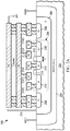
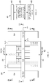
- Figures 2A through 2C and 3 illustrate varying layout views of a switch 200 in circuit 100 according to some embodiments.
- Figures 2A through 2C illustrate cross-sectional views of switch 200 while Figure 3 illustrates a corresponding top-down view of conductive lines over switch 200.
- Figure 2A illustrates a cross-section taken across line A-A of Figure 3
- Figure 2B illustrates a cross-section taken across line B-B of Figure 3
- 2C illustrates a cross-section taken across line C-C of Figure 3 .
- Switch 200 includes various isolation features provided by embodiment layout configurations as described in greater detail below.
- switch 200 is formed at a top surface of a semiconductor substrate 202.
- semiconductor substrate includes, for example, bulk silicon.
- substrate 202 may include another elementary semiconductor, such as germanium; a compound semiconductor including silicon carbide, gallium arsenic, gallium phosphide, indium phosphide, indium arsenide, and/or indium antimonide; an alloy semiconductor including SiGe, GaAsP, AlInAs, AlGaAs, GaInAs, GaInP, and/or GaInAsP; or combinations thereof.
- Other substrates such as multi-layered or gradient substrates, may also be used.
- Substrate 202 includes an isolation region 204 and an isolated dopant region 206.
- Isolation region 204 and isolated dopant region 206 may be doped with n-type and p-type dopants at any suitable concentration, and isolation region 204 and isolated dopant region 206 are doped with dopants of opposing types.
- isolation region 204 is a deep n-well (DNW) while dopant region 206 is a p-well for a p-type substrate.
- Switch 200 is disposed within dopant region 206. Isolation region 204 isolates dopant region 206 from stray energy in the surrounding substrate 202.
- isolation region 204 is disposed under and encircles a perimeter of dopant region 206.
- switch 200 is placed in the vicinity of numerous other active devices (e.g., other switches, transistors, diodes, and the like) also formed in substrate 202, and energy may leak from nearby devices into substrate 202.
- active devices e.g., other switches, transistors, diodes, and the like
- isolation region 204 is tied to power supply (e.g., by conductive lines and vias), which advantageously lowers isolation region 204's series resistance to supply.
- Switch 200 includes source/drain regions 210 (labeled 210' and 210") and gates 212 disposed between adjacent source/drain regions 210. Each source/drain region 210 is disposed on opposing sides of a corresponding gate 212. Source/drain regions 210 may be active regions of substrate 202, which are doped with dopants of a suitable type and concentration (e.g., N+ in the illustrated embodiments for an NMOS transistor). Gates 212 may include a gate dielectric (e.g., a high-k dielectric layer), a gate electrode (e.g., polysilicon or a metal) over the gate dielectric, and various interfacial/spacer/hard mask layers as applicable.
- a gate dielectric e.g., a high-k dielectric layer
- a gate electrode e.g., polysilicon or a metal
- switch 200 is configured as a dual-gate transistor (e.g., a two finger NMOS transistor) having two drain regions and one source region; however, any suitable transistor configuration (e.g., single gate transistors) may be used.
- any suitable transistor configuration e.g., single gate transistors
- Figure 2A illustrates switch 200 as an n-type transistor, a p-type transistor may also be used.
- the dopant type of various active areas e.g., isolation region 204, dopant region 206, source/drain regions, and dopant region 208) may be reversed.
- Dopant regions 208 having dopants of an opposing type as source/drain regions 210 are disposed adjacent to outer source/drain regions 210'within isolated dopant region 206.
- source/drain regions 210 are N+ regions and dopant region 208 are P+ regions.
- a dopant concentration of dopant region 208 may be higher than surrounding dopant region 206.
- Dopant regions 208 are electrically coupled to ground (e.g., electrically connected by an interconnect structure 216 to ground).
- the interconnect structure is referred to as a grounded conductive wall 216 hereinafter.
- Grounded conductive wall 216 includes conductive lines and vias formed in various dielectric layers using any suitable method.
- the dielectric layers may include low-k dielectric materials having k-values, for example, lower than about 4.0 or lower than about 2.0, formed by spinning, chemical vapor deposition (CVD), plasma-enhanced CVD (PECVD), and the like.
- CVD chemical vapor deposition
- PECVD plasma-enhanced CVD
- a patterning process e.g., a combination of photolithography and etching
- a conductive material e.g., copper, aluminum, tungsten, combinations thereof, and the like
- any suitable method e.g., electro-chemical plating, electroless plating, and the like
- Dopant regions 208 are included to collect energy injected into dopant region 206 by active regions of switch 200 (e.g., source/drain regions 210 and channel regions) when switch 200 is enabled or disabled. For example, when switch 200 is enabled (e.g., in an "on" state), dopant regions 208 are used to keep energy from escaping into the surrounding substrate 202. As another example, when switch 200 is disabled (e.g., in an "off' state), dopant regions 208 are used to lower the energy coupling between adjacent source/drain regions 210.Thus, dopant regions 208 may be used to reduce stray energy from accumulating in dopant region 206. Instead, dopant regions 208 collect and shunt this energy to electrical ground.
- active regions of switch 200 e.g., source/drain regions 210 and channel regions
- dopant regions 208 are disposed adjacent (e.g., as close as possible) to active source/drain regions 210 for improved energy collection. Dopant region 208 may also collect energy injected into dopant region 206 through the isolation region 204 from the surrounding substrate 202.
- Gates 212 are electrically coupled to a control circuit (e.g., controller 150), which selects whether to pass an input signal to an output of switch 200 by turning switch 200 "on” or “off'.
- a source/drain region 210" is electrically coupled to an input signal 102/104.
- source/drain regions 210" are electrically connected to input signal 102/104 by conductive lines 2141 as illustrated by Figure 2B and 3 .
- Source/drain regions 210' are electrically coupled to an output signal 106.
- source/drain regions 210' are electrically connected to output signal 106 by conductive lines 2140 as illustrated by Figures 2C and 3 .
- the configuration of the input and output signals may be reversed depending on whether the input signal or the output signal benefits from less parasitic capacitance.
- the source/drain region 210" may be electrically connected to an output signal 106 by conductive line 2141 (an M1 line) and 2201 (an M6 line). In the illustrated embodiments, less parasitic capacitance is desired at the input, so the input of the switch is connected to a conductive line 2141 and 2201.
- grounded conductive lines 214' are disposed between adjacent conductive lines 2141 and 2140. Grounded conductive lines 214' are electrically coupled to ground. For example, grounded conductive wall 216 may electrically connect conductive lines 214' to ground, and grounded conductive lines 214' may be used to pass coupled energy from source/drain regions 210 when switch 200 is disabled to ground. Grounded conductive lines 214' are aligned between adjacent source/drain regions 210 in semiconductor substrate 202. For example, at least a portion of each grounded conductive lines 214' is aligned with a gate 212. A geometric line substantially perpendicular with a lateral surface of the substrate may intersect both gate 212 and grounded conductive line 214'.
- an active area of switch 200 may be increased to accommodate the placement of grounded conductive lines 214' above and aligned between source/drain regions 210.
- gates 212 may further be positioned to reduce capacitance of the active area on the input rather than the output to further reduce power consumption.
- outer source/drain regions 210' are configured to have a larger lateral dimension. This configuration also accommodates the placement of conductive lines 214' aligned between adjacent source/drain regions 210.
- Figures 2B and 2C illustrate cross-sectional views of input/output lines 220.
- input line 2201 provides an input signal 102/104 to conductive line 2141 (e.g., an M1 line), which is electrically connected to an inner source/drain region 210" of switch 200.
- output line 2200 is used to take an output signal 106 from conductive line 2140 (e.g., an M1 line), which is electrically connected to an outer source/drain region 210' of switch 200.
- input and output lines 220 are disposed in higher metal layers than M1 to reduce electrical coupling with substrate 202.
- input and output lines 220 are further positioned in non-adjacent metal layers to reduce coupling between input line 2201 and output line 2200, particularly in areas where input line 2201 and output line 2200 intersect.
- input line 2201 is in conductive line layer M6 while output line 2200 is in conductive line layer M4.
- At least one conductive line layer (M5) is disposed between input line 2201 and output line 2200.
- the specific metal layer configuration illustrated is but one example embodiment, and various conductive lines may be disposed in other configurations.
- the output line 2200 may be disposed in a higher conductive line layer than input line 2201 in another embodiment.
- various conductive interconnect features 218 are used to electrically connect input line 2201 in a higher conductive line layer (e.g., M6) to conductive line 2141 in layer M1.
- various conductive interconnect features 222 are used to electrically connect output line 2200 in a higher conductive line layer (e.g., M4) to conductive line 2140 in layer M1.
- input/output lines and interconnect features 218/222 may be formed of similar materials using similar methods as grounded conductive wall 216 as described above. Isolation features are included to reduce electrical coupling between interconnect features 218 and 222.
- a grounded conductive wall 216 may be disposed between interconnect features 218 and 222 as illustrated by Figure 3 .
- Grounded conductive wall 216 includes conductive lines in layers M1 through M5 and provides a wall of electrical isolation in layers having both interconnect features 218 and 222 (e.g., layers M1 through M4). Additional redistribution layers having conductive lines/vias (e.g., providing signals, power, and/or ground) may also be included in circuit 100. Other features such as contact pads, passivation layers, solder balls, and the like may also be formed over the redistribution layers as part of a device die containing circuit 100.
- a switch for improved isolation.
- Such a switch may be used in an integrated circuit where such isolation is desirable in lieu of multi-switch isolation circuits, thus reducing power consumption of the device.
- simulations were conducted using a switch having isolation features as described above in a circuit similar to circuit layout 100. A realistic load was placed at the output and each input was driven by a different frequency signal (e.g., a first frequency of 4GHz and a second frequency of 4.2GHz). One switch was disabled while the other was enabled. The switch and its load were laid out and extracted.
- the passed signal had a magnitude of 0.24 dB while the disabled signal had a magnitude of -78.5 dB, for a difference of 78.7 dB.
- An isolation target for these types of circuits is about 70 dB.
- FIG. 4 illustrates a process flow 400 for configuring a switch according to various embodiments.
- a switch e.g., switch 200
- the switch includes at least one gate (e.g., gate 212) with a first source/drain region (e.g., source/drain region 210") and a second source/drain region (e.g., source/drain region 210') formed on opposing sides of the gate.
- the source/drain regions may further be disposed at a top surface of a semiconductor substrate, for example, within an isolated dopant region (e.g., dopant region 206).
- a conductive line e.g., conductive line 214'
- the conductive line may be vertically aligned between the first and second source/drain regions. For example, at least a portion of the conductive line may by vertically aligned with the gate.
- the conductive line is formed in layer M1 (e.g., a conductive line layer closest and immediately above the semiconductor substrate). In such embodiments, no other conductive lines are formed between the conductive line and the semiconductor substrate.
- the conductive line is electrically connected to ground, for example by a grounded conductive wall (e.g., wall 216).
Landscapes
- Semiconductor Integrated Circuits (AREA)
- Design And Manufacture Of Integrated Circuits (AREA)
- Physics & Mathematics (AREA)
- Geometry (AREA)
- Metal-Oxide And Bipolar Metal-Oxide Semiconductor Integrated Circuits (AREA)
Claims (12)
- Integrierte Schaltung (100), die Folgendes umfasst:• einen Schalter (200), der Folgendes umfasst:∘ einen Gate-Kontakt (212);∘ eine erste Source/Drain-Region (210") an einer oberen Oberfläche eines Halbleitersubstrats (202) des Schalters (200); und∘ eine zweite Source/Drain-Region (210') an der oberen Oberfläche des Halbleitersubstrats, wobei die erste Source/Drain-Region (210") und die zweite Source/Drain-Region (210') an einander gegenüberliegenden Seiten des Gate-Kontakts (212) angeordnet sind; und• eine erste leitfähige Leitung (214'), bereitgestellt in einer ersten Richtung über dem Schalter (200), wobei zumindest ein Teil der ersten leitfähigen Leitung (214') mit dem Gate-Kontakt (212) ausgerichtet ist und wobei die erste leitfähige Leitung (214') elektrisch mit Masse gekoppelt ist, wobei die erste Richtung eine Richtung senkrecht zur oberen Oberfläche des Halbleitersubstrats (202) ist und sich vom Halbleitersubstrat (202) weg erstreckt;• eine zweite leitfähige Leitung (214I) in einer gleichen Schicht (M1) wie die erste leitfähige Leitung (214'), wobei die zweite leitfähige Leitung (214I) elektrisch mit der ersten Source/Drain-Region (210") verbunden ist;• eine dritte leitfähige Leitung (2140) in der gleichen Schicht (M1) wie die erste leitfähige Leitung (214'), wobei die dritte leitfähige Leitung (2140) elektrisch mit der zweiten Source/Drain-Region (210') verbunden ist und wobei die erste leitfähige Leitung (214') zwischen der zweiten leitfähigen Leitung (214I) und der dritten leitfähigen Leitung (2140) angeordnet ist;• erste Verbindungsmerkmale (218), die die zweite leitfähige Leitung (214I) mit einer Eingangsleitung (220I) der integrierten Schaltung (100) verbinden, wobei die Eingangsleitung (220I) in einer ersten leitfähigen Leitungsschicht (M6) der integrierten Schaltung (100) angeordnet ist und die Eingangsleitung (220I) in der ersten Richtung höher als die zweite leitfähige Leitung (214I) angeordnet ist; und• zweite Verbindungsmerkmale (222), die die dritte leitfähige Leitung (2140) elektrisch mit einer Ausgangsleitung (2200) der integrierten Schaltung (100) verbinden, wobei die Ausgangsleitung (2200) in einer zweiten leitfähigen Leitungsschicht (M4) der integrierten Schaltung (100) angeordnet ist und die Ausgangsleitung (2200) in der ersten Richtung höher als die dritte leitfähige Leitung (214O) angeordnet ist.
- Integrierte Schaltung nach Anspruch 1, ferner umfassend dritte Verbindungsmerkmale (216), angeordnet zwischen den ersten Verbindungsmerkmalen (218) und den zweiten Verbindungsmerkmalen (222), wobei die dritten Verbindungsmerkmale (216) elektrisch mit Masse gekoppelt sind.
- Integrierte Schaltung nach Anspruch 2, wobei die erste leitfähige Leitung (214') über die dritten Verbindungsmerkmale (216) elektrisch mit Masse gekoppelt ist.
- Integrierte Schaltung nach Anspruch 1, wobei die Eingangsleitung (220I) und die Ausgangsleitung (2200) in zwei unterschiedlichen leitfähigen Leitungsschichten angeordnet sind, wobei die zwei unterschiedlichen leitfähigen Leitungsschichten nicht angrenzend sind.
- Integrierte Schaltung nach einem der Ansprüche 1 bis 4, ferner umfassend eine Dotandenregion (208) angrenzend an die erste Source/Drain-Region (210") oder die zweite Source/Drain-Region (210'), wobei die Dotandenregion (208) Dotanden von einem entgegengesetzten Typ zur ersten Source/Drain-Region (210") umfasst und wobei die Dotandenregion (208) elektrisch mit Masse verbunden ist.
- Integrierte Schaltung nach einem der Ansprüche 1 bis 5, wobei die erste Source/Drain-Region (210") und die zweite Source/Drain-Region (210') innerhalb einer isolierten Dotandenregion (206) eines Halbleitersubstrats (202) angeordnet sind, wobei die isolierte Dotandenregion (206) von einem entgegengesetzten Typ zur ersten Source/Drain-Region (210") und zur zweiten Source/Drain-Region (210') ist.
- Integrierte Schaltung nach Anspruch 6, ferner umfassend eine Isolationsregion (204), die die isolierte Dotandenregion (206) umschließt und unter dieser angeordnet ist, wobei die Isolationsregion (204) Dotanden von einem entgegengesetzten Typ zur isolierten Dotandenregion (206) umfasst.
- Integrierte Schaltung nach Anspruch 7, wobei die Isolationsregion (204) elektrisch mit der Zufuhrspannung verbunden ist.
- Verfahren, das Folgendes umfasst:• Bereitstellen eines Schalters (200), der Folgendes umfasst:∘ einen Gate-Kontakt (212);∘ eine erste Source/Drain-Region (210") an einer oberen Oberfläche eines Halbleitersubstrats (202) des Schalters (200); und∘ eine zweite Source/Drain-Region (210') an der oberen Oberfläche des Halbleitersubstrats (202), wobei die erste Source/Drain-Region (210") und die zweite Source/Drain-Region (210') an einander gegenüberliegenden Seiten des Gate-Kontakts (212) angeordnet sind;• Bilden einer ersten leitfähigen Leitung (214') in einer ersten Richtung über dem Schalter (200), wobei zumindest ein Teil der ersten leitfähigen Leitung (214') mit dem Gate-Kontakt (212) ausgerichtet ist, wobei die erste Richtung eine Richtung senkrecht zur oberen Oberfläche des Halbleitersubstrats (202) ist und sich vom Halbleitersubstrat (202) weg erstreckt;• elektrisches Koppeln der ersten leitfähigen Leitung (214') mit Masse;• Bilden einer zweiten leitfähigen Leitung (214I), elektrisch mit der ersten Source/Drain-Region (210") in einer gleichen Schicht (M1) wie die erste leitfähige Leitung (214') verbunden;• Bilden einer dritten leitfähigen Leitung (2140), elektrisch mit der zweiten Source/Drain-Region (210') in der gleichen Schicht (M1) wie die erste leitfähige Leitung (214') verbunden, wobei die erste leitfähige Leitung (214') zwischen der zweiten leitfähigen Leitung (214I) und der dritten leitfähigen Leitung (2140) angeordnet ist;• Bilden von ersten Verbindungsmerkmalen (218), die die zweite leitfähige Leitung (214I) elektrisch mit einer Eingangsleitung (220I) verbinden;• Bereitstellen einer ersten leitfähigen Leitungsschicht (M6) und Bilden der Eingangsleitung (220I) in der ersten leitfähigen Leitungsschicht (M6), wobei die Eingangsleitung (220I) in der ersten Richtung höher als die zweite leitfähige Leitung (214I) angeordnet ist;• Bilden von zweiten Verbindungsmerkmalen (222), die die dritte leitfähige Leitung (214O) elektrisch mit einer Ausgangsleitung (2200) verbinden; und• Bereitstellen einer zweiten leitfähigen Leitungsschicht (M4) und Bilden der Ausgangsleitung (2200) in der zweiten leitfähigen Leitungsschicht (M4), wobei die Ausgangsleitung (2200) in der ersten Richtung höher als die dritte leitfähige Leitung (214O) angeordnet ist;
- Verfahren nach Anspruch 9, das ferner Folgendes umfasst: Bilden von dritten Verbindungsmerkmalen (216) zwischen den ersten Verbindungsmerkmalen (218) und den zweiten Verbindungsmerkmalen (222); und elektrisches Koppeln der dritten Verbindungsmerkmale (216) mit Masse.
- Verfahren nach einem der Ansprüche 9 bis 10, wobei Bereitstellen des Schalters (200) Bilden der ersten Source/Drain-Region (210") und der zweiten Source/Drain-Region (210') in einer isolierten Dotandenregion (206) eines Halbleitersubstrats umfasst, wobei die isolierte Dotandenregion (206) Dotanden von einem entgegengesetzten Typ zur ersten Source/Drain-Region (210") und zur zweiten Source/Drain-Region (210') umfasst.
- Verfahren nach Anspruch 11, das ferner Folgendes umfasst: Bilden einer Dotandenregion (208) in der isolierten Dotandenregion (206), wobei die Dotandenregion (208) Dotanden von einem entgegengesetzten Typ zur ersten Source/Drain-Region (210") und zur zweiten Source/Drain-Region (210') umfasst; und elektrisches Koppeln der Dotandenregion (208) mit der elektrischen Masse.
Priority Applications (1)
| Application Number | Priority Date | Filing Date | Title |
|---|---|---|---|
| EP21181089.0A EP3929977B1 (de) | 2015-06-03 | 2016-06-02 | Vorrichtung für einen schalter mit hoher isolation |
Applications Claiming Priority (2)
| Application Number | Priority Date | Filing Date | Title |
|---|---|---|---|
| US14/730,018 US9449969B1 (en) | 2015-06-03 | 2015-06-03 | Device and method for a high isolation switch |
| PCT/CN2016/084425 WO2016192645A1 (en) | 2015-06-03 | 2016-06-02 | Device and method for a high isolation switch |
Related Child Applications (2)
| Application Number | Title | Priority Date | Filing Date |
|---|---|---|---|
| EP21181089.0A Division EP3929977B1 (de) | 2015-06-03 | 2016-06-02 | Vorrichtung für einen schalter mit hoher isolation |
| EP21181089.0A Division-Into EP3929977B1 (de) | 2015-06-03 | 2016-06-02 | Vorrichtung für einen schalter mit hoher isolation |
Publications (3)
| Publication Number | Publication Date |
|---|---|
| EP3304739A1 EP3304739A1 (de) | 2018-04-11 |
| EP3304739A4 EP3304739A4 (de) | 2018-05-30 |
| EP3304739B1 true EP3304739B1 (de) | 2021-08-04 |
Family
ID=56896197
Family Applications (2)
| Application Number | Title | Priority Date | Filing Date |
|---|---|---|---|
| EP21181089.0A Active EP3929977B1 (de) | 2015-06-03 | 2016-06-02 | Vorrichtung für einen schalter mit hoher isolation |
| EP16802568.2A Active EP3304739B1 (de) | 2015-06-03 | 2016-06-02 | Vorrichtung und verfahren für einen schalter mit hoher isolation |
Family Applications Before (1)
| Application Number | Title | Priority Date | Filing Date |
|---|---|---|---|
| EP21181089.0A Active EP3929977B1 (de) | 2015-06-03 | 2016-06-02 | Vorrichtung für einen schalter mit hoher isolation |
Country Status (4)
| Country | Link |
|---|---|
| US (2) | US9449969B1 (de) |
| EP (2) | EP3929977B1 (de) |
| CN (3) | CN112466843A (de) |
| WO (1) | WO2016192645A1 (de) |
Family Cites Families (24)
| Publication number | Priority date | Publication date | Assignee | Title |
|---|---|---|---|---|
| US5324982A (en) * | 1985-09-25 | 1994-06-28 | Hitachi, Ltd. | Semiconductor memory device having bipolar transistor and structure to avoid soft error |
| JPH06223568A (ja) * | 1993-01-29 | 1994-08-12 | Mitsubishi Electric Corp | 中間電位発生装置 |
| EP1699084B1 (de) * | 1995-04-12 | 2011-05-25 | Fuji Electric Systems Co., Ltd. | Integrierter Hochspannungsschaltkreis, Hochspannungsübergangsabschluss- struktur und MIS-Hochspannungstransistor |
| US6744117B2 (en) * | 2002-02-28 | 2004-06-01 | Motorola, Inc. | High frequency semiconductor device and method of manufacture |
| JP2004006816A (ja) * | 2002-04-17 | 2004-01-08 | Sanyo Electric Co Ltd | 半導体スイッチ回路装置およびその製造方法 |
| JP2003309130A (ja) * | 2002-04-17 | 2003-10-31 | Sanyo Electric Co Ltd | 半導体スイッチ回路装置 |
| JP2006261154A (ja) * | 2005-03-15 | 2006-09-28 | Seiko Instruments Inc | 半導体装置およびその設計方法 |
| US7345545B2 (en) * | 2005-03-28 | 2008-03-18 | Freescale Semiconductor, Inc. | Enhancement mode transceiver and switched gain amplifier integrated circuit |
| JP4186970B2 (ja) * | 2005-06-30 | 2008-11-26 | セイコーエプソン株式会社 | 集積回路装置及び電子機器 |
| JP4151688B2 (ja) * | 2005-06-30 | 2008-09-17 | セイコーエプソン株式会社 | 集積回路装置及び電子機器 |
| CN101231998B (zh) * | 2007-01-23 | 2011-01-26 | 米辑电子股份有限公司 | 一种线路组件 |
| KR100976627B1 (ko) * | 2007-12-10 | 2010-08-18 | 한국전자통신연구원 | 밀리미터파 대역 제어회로용 스위치 회로 |
| US8853832B2 (en) * | 2009-01-22 | 2014-10-07 | Stmicroelectronics Inc. | Methods and apparatus for reducing coupling in a MOS device |
| KR101197379B1 (ko) * | 2009-02-20 | 2012-11-05 | 존 린치 | 전류제어기를 갖고 전력소비가 적은 메모리장치 |
| US7924102B2 (en) * | 2009-02-23 | 2011-04-12 | Qualcomm Incorporated | Symmetric load delay cell oscillator |
| CN101702627B (zh) * | 2009-10-29 | 2012-10-03 | 华东师范大学 | 一种基于绝缘体上硅工艺的cmos射频开关 |
| US8278720B2 (en) * | 2010-03-29 | 2012-10-02 | Avago Technologies Wireless Ip (Singapore) Pte. Ltd. | Field effect transistor switch for RF signals and method of making the same |
| US8330530B2 (en) * | 2010-06-07 | 2012-12-11 | Skyworks Solutions, Inc. | Apparatus and method for disabling well bias |
| US8288235B2 (en) * | 2010-10-20 | 2012-10-16 | Globalfoundries Singapore Pte. Ltd. | Self-aligned body fully isolated device |
| US8664717B2 (en) * | 2012-01-09 | 2014-03-04 | Globalfoundries Inc. | Semiconductor device with an oversized local contact as a Faraday shield |
| US9148194B2 (en) * | 2012-07-07 | 2015-09-29 | Skyworks Solutions, Inc. | Radio-frequency switch system having improved intermodulation distortion performance |
| US9490248B2 (en) * | 2012-12-31 | 2016-11-08 | Taiwan Semiconductor Manufacturing Company, Ltd. | Power cell, power cell circuit for a power amplifier and a method of making and using a power cell |
| JP5885712B2 (ja) * | 2013-08-22 | 2016-03-15 | 株式会社東芝 | スイッチ回路 |
| EP3506504B1 (de) * | 2013-11-12 | 2021-09-01 | Skyworks Solutions, Inc. | Vorrichtungen und verfahren in zusammenhang mit hochfrequenzschaltern mit verbesserter leistung |
-
2015
- 2015-06-03 US US14/730,018 patent/US9449969B1/en active Active
-
2016
- 2016-06-02 EP EP21181089.0A patent/EP3929977B1/de active Active
- 2016-06-02 CN CN202011247236.7A patent/CN112466843A/zh active Pending
- 2016-06-02 EP EP16802568.2A patent/EP3304739B1/de active Active
- 2016-06-02 CN CN201680032693.XA patent/CN107710618B/zh active Active
- 2016-06-02 WO PCT/CN2016/084425 patent/WO2016192645A1/en not_active Ceased
- 2016-06-02 CN CN202011247239.0A patent/CN112466844A/zh active Pending
- 2016-09-02 US US15/256,154 patent/US9768165B2/en active Active
Non-Patent Citations (1)
| Title |
|---|
| None * |
Also Published As
| Publication number | Publication date |
|---|---|
| US9768165B2 (en) | 2017-09-19 |
| EP3929977A1 (de) | 2021-12-29 |
| CN107710618B (zh) | 2020-11-17 |
| EP3304739A4 (de) | 2018-05-30 |
| US20160372464A1 (en) | 2016-12-22 |
| US9449969B1 (en) | 2016-09-20 |
| EP3929977B1 (de) | 2025-03-12 |
| EP3304739A1 (de) | 2018-04-11 |
| CN112466843A (zh) | 2021-03-09 |
| CN107710618A (zh) | 2018-02-16 |
| CN112466844A (zh) | 2021-03-09 |
| WO2016192645A1 (en) | 2016-12-08 |
Similar Documents
| Publication | Publication Date | Title |
|---|---|---|
| US10734384B1 (en) | Vertically-integrated two-dimensional (2D) semiconductor slabs in complementary field effect transistor (CFET) cell circuits, and method of fabricating | |
| US10861852B2 (en) | Three-dimensional (3D), vertically-integrated field-effect transistors (FETs) for complementary metal-oxide semiconductor (CMOS) cell circuits | |
| US8659126B2 (en) | Integrated circuit ground shielding structure | |
| US9922973B1 (en) | Switches with deep trench depletion and isolation structures | |
| TWI443836B (zh) | 於共同基板上之功率裝置整合 | |
| US7022566B2 (en) | Integrated radio frequency circuits | |
| TWI591803B (zh) | 於共同基板上之功率裝置整合 | |
| US10243047B2 (en) | Active and passive components with deep trench isolation structures | |
| TWI536461B (zh) | 射頻裝置及射頻裝置之製造方法 | |
| TW201409610A (zh) | 於共同基板上之功率裝置整合 | |
| US8957496B2 (en) | Integrated circuit chip with discontinuous guard ring | |
| WO2005098937A1 (en) | Techniques to reduce substrate cross talk on mixed signal and rf circuit design | |
| KR100954919B1 (ko) | 반도체 소자용 인덕터 및 그 제조 방법 | |
| EP3304739B1 (de) | Vorrichtung und verfahren für einen schalter mit hoher isolation | |
| WO2018063397A1 (en) | Gate trench precision resistors with high-k rmg gan transistor | |
| EP4018482A1 (de) | Integrierte vorrichtung mit einer cmos-struktur mit leiterlosen transistoren | |
| CN102983140B (zh) | 半导体结构及其制造方法 | |
| US20250063822A1 (en) | Contact Structures for Dual-Thickness Active Area SOI FETS | |
| US20240429239A1 (en) | Dual-Thickness Active Area Architecture for SOI FETS | |
| US8546907B2 (en) | Enhanced transmission lines for radio frequency applications | |
| CN101866919A (zh) | 集成电路结构 |
Legal Events
| Date | Code | Title | Description |
|---|---|---|---|
| STAA | Information on the status of an ep patent application or granted ep patent |
Free format text: STATUS: THE INTERNATIONAL PUBLICATION HAS BEEN MADE |
|
| PUAI | Public reference made under article 153(3) epc to a published international application that has entered the european phase |
Free format text: ORIGINAL CODE: 0009012 |
|
| STAA | Information on the status of an ep patent application or granted ep patent |
Free format text: STATUS: REQUEST FOR EXAMINATION WAS MADE |
|
| 17P | Request for examination filed |
Effective date: 20171218 |
|
| AK | Designated contracting states |
Kind code of ref document: A1 Designated state(s): AL AT BE BG CH CY CZ DE DK EE ES FI FR GB GR HR HU IE IS IT LI LT LU LV MC MK MT NL NO PL PT RO RS SE SI SK SM TR |
|
| AX | Request for extension of the european patent |
Extension state: BA ME |
|
| REG | Reference to a national code |
Ref country code: DE Ref legal event code: R079 Ref document number: 602016061676 Country of ref document: DE Free format text: PREVIOUS MAIN CLASS: H03K0017687000 Ipc: H01L0023522000 |
|
| A4 | Supplementary search report drawn up and despatched |
Effective date: 20180503 |
|
| RIC1 | Information provided on ipc code assigned before grant |
Ipc: H01L 29/06 20060101ALI20180425BHEP Ipc: H01L 29/78 20060101ALI20180425BHEP Ipc: H01L 27/088 20060101ALI20180425BHEP Ipc: H04B 1/44 20060101ALI20180425BHEP Ipc: H03K 17/687 20060101ALI20180425BHEP Ipc: H01L 23/522 20060101AFI20180425BHEP Ipc: H01L 21/761 20060101ALI20180425BHEP Ipc: H01L 29/10 20060101ALI20180425BHEP |
|
| DAV | Request for validation of the european patent (deleted) | ||
| DAX | Request for extension of the european patent (deleted) | ||
| STAA | Information on the status of an ep patent application or granted ep patent |
Free format text: STATUS: EXAMINATION IS IN PROGRESS |
|
| 17Q | First examination report despatched |
Effective date: 20200331 |
|
| GRAP | Despatch of communication of intention to grant a patent |
Free format text: ORIGINAL CODE: EPIDOSNIGR1 |
|
| STAA | Information on the status of an ep patent application or granted ep patent |
Free format text: STATUS: GRANT OF PATENT IS INTENDED |
|
| INTG | Intention to grant announced |
Effective date: 20210318 |
|
| GRAS | Grant fee paid |
Free format text: ORIGINAL CODE: EPIDOSNIGR3 |
|
| GRAA | (expected) grant |
Free format text: ORIGINAL CODE: 0009210 |
|
| STAA | Information on the status of an ep patent application or granted ep patent |
Free format text: STATUS: THE PATENT HAS BEEN GRANTED |
|
| AK | Designated contracting states |
Kind code of ref document: B1 Designated state(s): AL AT BE BG CH CY CZ DE DK EE ES FI FR GB GR HR HU IE IS IT LI LT LU LV MC MK MT NL NO PL PT RO RS SE SI SK SM TR |
|
| REG | Reference to a national code |
Ref country code: GB Ref legal event code: FG4D |
|
| REG | Reference to a national code |
Ref country code: AT Ref legal event code: REF Ref document number: 1417863 Country of ref document: AT Kind code of ref document: T Effective date: 20210815 |
|
| REG | Reference to a national code |
Ref country code: CH Ref legal event code: EP |
|
| REG | Reference to a national code |
Ref country code: DE Ref legal event code: R096 Ref document number: 602016061676 Country of ref document: DE |
|
| REG | Reference to a national code |
Ref country code: IE Ref legal event code: FG4D |
|
| REG | Reference to a national code |
Ref country code: LT Ref legal event code: MG9D |
|
| REG | Reference to a national code |
Ref country code: NL Ref legal event code: MP Effective date: 20210804 |
|
| REG | Reference to a national code |
Ref country code: AT Ref legal event code: MK05 Ref document number: 1417863 Country of ref document: AT Kind code of ref document: T Effective date: 20210804 |
|
| PG25 | Lapsed in a contracting state [announced via postgrant information from national office to epo] |
Ref country code: LT Free format text: LAPSE BECAUSE OF FAILURE TO SUBMIT A TRANSLATION OF THE DESCRIPTION OR TO PAY THE FEE WITHIN THE PRESCRIBED TIME-LIMIT Effective date: 20210804 Ref country code: AT Free format text: LAPSE BECAUSE OF FAILURE TO SUBMIT A TRANSLATION OF THE DESCRIPTION OR TO PAY THE FEE WITHIN THE PRESCRIBED TIME-LIMIT Effective date: 20210804 Ref country code: BG Free format text: LAPSE BECAUSE OF FAILURE TO SUBMIT A TRANSLATION OF THE DESCRIPTION OR TO PAY THE FEE WITHIN THE PRESCRIBED TIME-LIMIT Effective date: 20211104 Ref country code: HR Free format text: LAPSE BECAUSE OF FAILURE TO SUBMIT A TRANSLATION OF THE DESCRIPTION OR TO PAY THE FEE WITHIN THE PRESCRIBED TIME-LIMIT Effective date: 20210804 Ref country code: ES Free format text: LAPSE BECAUSE OF FAILURE TO SUBMIT A TRANSLATION OF THE DESCRIPTION OR TO PAY THE FEE WITHIN THE PRESCRIBED TIME-LIMIT Effective date: 20210804 Ref country code: FI Free format text: LAPSE BECAUSE OF FAILURE TO SUBMIT A TRANSLATION OF THE DESCRIPTION OR TO PAY THE FEE WITHIN THE PRESCRIBED TIME-LIMIT Effective date: 20210804 Ref country code: NO Free format text: LAPSE BECAUSE OF FAILURE TO SUBMIT A TRANSLATION OF THE DESCRIPTION OR TO PAY THE FEE WITHIN THE PRESCRIBED TIME-LIMIT Effective date: 20211104 Ref country code: PT Free format text: LAPSE BECAUSE OF FAILURE TO SUBMIT A TRANSLATION OF THE DESCRIPTION OR TO PAY THE FEE WITHIN THE PRESCRIBED TIME-LIMIT Effective date: 20211206 Ref country code: RS Free format text: LAPSE BECAUSE OF FAILURE TO SUBMIT A TRANSLATION OF THE DESCRIPTION OR TO PAY THE FEE WITHIN THE PRESCRIBED TIME-LIMIT Effective date: 20210804 Ref country code: SE Free format text: LAPSE BECAUSE OF FAILURE TO SUBMIT A TRANSLATION OF THE DESCRIPTION OR TO PAY THE FEE WITHIN THE PRESCRIBED TIME-LIMIT Effective date: 20210804 |
|
| PG25 | Lapsed in a contracting state [announced via postgrant information from national office to epo] |
Ref country code: PL Free format text: LAPSE BECAUSE OF FAILURE TO SUBMIT A TRANSLATION OF THE DESCRIPTION OR TO PAY THE FEE WITHIN THE PRESCRIBED TIME-LIMIT Effective date: 20210804 Ref country code: LV Free format text: LAPSE BECAUSE OF FAILURE TO SUBMIT A TRANSLATION OF THE DESCRIPTION OR TO PAY THE FEE WITHIN THE PRESCRIBED TIME-LIMIT Effective date: 20210804 Ref country code: GR Free format text: LAPSE BECAUSE OF FAILURE TO SUBMIT A TRANSLATION OF THE DESCRIPTION OR TO PAY THE FEE WITHIN THE PRESCRIBED TIME-LIMIT Effective date: 20211105 |
|
| PG25 | Lapsed in a contracting state [announced via postgrant information from national office to epo] |
Ref country code: NL Free format text: LAPSE BECAUSE OF FAILURE TO SUBMIT A TRANSLATION OF THE DESCRIPTION OR TO PAY THE FEE WITHIN THE PRESCRIBED TIME-LIMIT Effective date: 20210804 |
|
| PG25 | Lapsed in a contracting state [announced via postgrant information from national office to epo] |
Ref country code: DK Free format text: LAPSE BECAUSE OF FAILURE TO SUBMIT A TRANSLATION OF THE DESCRIPTION OR TO PAY THE FEE WITHIN THE PRESCRIBED TIME-LIMIT Effective date: 20210804 |
|
| REG | Reference to a national code |
Ref country code: DE Ref legal event code: R097 Ref document number: 602016061676 Country of ref document: DE |
|
| PG25 | Lapsed in a contracting state [announced via postgrant information from national office to epo] |
Ref country code: SM Free format text: LAPSE BECAUSE OF FAILURE TO SUBMIT A TRANSLATION OF THE DESCRIPTION OR TO PAY THE FEE WITHIN THE PRESCRIBED TIME-LIMIT Effective date: 20210804 Ref country code: SK Free format text: LAPSE BECAUSE OF FAILURE TO SUBMIT A TRANSLATION OF THE DESCRIPTION OR TO PAY THE FEE WITHIN THE PRESCRIBED TIME-LIMIT Effective date: 20210804 Ref country code: RO Free format text: LAPSE BECAUSE OF FAILURE TO SUBMIT A TRANSLATION OF THE DESCRIPTION OR TO PAY THE FEE WITHIN THE PRESCRIBED TIME-LIMIT Effective date: 20210804 Ref country code: EE Free format text: LAPSE BECAUSE OF FAILURE TO SUBMIT A TRANSLATION OF THE DESCRIPTION OR TO PAY THE FEE WITHIN THE PRESCRIBED TIME-LIMIT Effective date: 20210804 Ref country code: CZ Free format text: LAPSE BECAUSE OF FAILURE TO SUBMIT A TRANSLATION OF THE DESCRIPTION OR TO PAY THE FEE WITHIN THE PRESCRIBED TIME-LIMIT Effective date: 20210804 Ref country code: AL Free format text: LAPSE BECAUSE OF FAILURE TO SUBMIT A TRANSLATION OF THE DESCRIPTION OR TO PAY THE FEE WITHIN THE PRESCRIBED TIME-LIMIT Effective date: 20210804 |
|
| PLBE | No opposition filed within time limit |
Free format text: ORIGINAL CODE: 0009261 |
|
| STAA | Information on the status of an ep patent application or granted ep patent |
Free format text: STATUS: NO OPPOSITION FILED WITHIN TIME LIMIT |
|
| 26N | No opposition filed |
Effective date: 20220506 |
|
| PG25 | Lapsed in a contracting state [announced via postgrant information from national office to epo] |
Ref country code: IT Free format text: LAPSE BECAUSE OF FAILURE TO SUBMIT A TRANSLATION OF THE DESCRIPTION OR TO PAY THE FEE WITHIN THE PRESCRIBED TIME-LIMIT Effective date: 20210804 |
|
| PG25 | Lapsed in a contracting state [announced via postgrant information from national office to epo] |
Ref country code: SI Free format text: LAPSE BECAUSE OF FAILURE TO SUBMIT A TRANSLATION OF THE DESCRIPTION OR TO PAY THE FEE WITHIN THE PRESCRIBED TIME-LIMIT Effective date: 20210804 |
|
| PG25 | Lapsed in a contracting state [announced via postgrant information from national office to epo] |
Ref country code: MC Free format text: LAPSE BECAUSE OF FAILURE TO SUBMIT A TRANSLATION OF THE DESCRIPTION OR TO PAY THE FEE WITHIN THE PRESCRIBED TIME-LIMIT Effective date: 20210804 |
|
| REG | Reference to a national code |
Ref country code: CH Ref legal event code: PL |
|
| REG | Reference to a national code |
Ref country code: BE Ref legal event code: MM Effective date: 20220630 |
|
| GBPC | Gb: european patent ceased through non-payment of renewal fee |
Effective date: 20220602 |
|
| PG25 | Lapsed in a contracting state [announced via postgrant information from national office to epo] |
Ref country code: LU Free format text: LAPSE BECAUSE OF NON-PAYMENT OF DUE FEES Effective date: 20220602 Ref country code: LI Free format text: LAPSE BECAUSE OF NON-PAYMENT OF DUE FEES Effective date: 20220630 Ref country code: IE Free format text: LAPSE BECAUSE OF NON-PAYMENT OF DUE FEES Effective date: 20220602 Ref country code: FR Free format text: LAPSE BECAUSE OF NON-PAYMENT OF DUE FEES Effective date: 20220630 Ref country code: CH Free format text: LAPSE BECAUSE OF NON-PAYMENT OF DUE FEES Effective date: 20220630 |
|
| PG25 | Lapsed in a contracting state [announced via postgrant information from national office to epo] |
Ref country code: GB Free format text: LAPSE BECAUSE OF NON-PAYMENT OF DUE FEES Effective date: 20220602 Ref country code: BE Free format text: LAPSE BECAUSE OF NON-PAYMENT OF DUE FEES Effective date: 20220630 |
|
| P01 | Opt-out of the competence of the unified patent court (upc) registered |
Effective date: 20230524 |
|
| PG25 | Lapsed in a contracting state [announced via postgrant information from national office to epo] |
Ref country code: HU Free format text: LAPSE BECAUSE OF FAILURE TO SUBMIT A TRANSLATION OF THE DESCRIPTION OR TO PAY THE FEE WITHIN THE PRESCRIBED TIME-LIMIT; INVALID AB INITIO Effective date: 20160602 |
|
| PG25 | Lapsed in a contracting state [announced via postgrant information from national office to epo] |
Ref country code: MK Free format text: LAPSE BECAUSE OF FAILURE TO SUBMIT A TRANSLATION OF THE DESCRIPTION OR TO PAY THE FEE WITHIN THE PRESCRIBED TIME-LIMIT Effective date: 20210804 Ref country code: CY Free format text: LAPSE BECAUSE OF FAILURE TO SUBMIT A TRANSLATION OF THE DESCRIPTION OR TO PAY THE FEE WITHIN THE PRESCRIBED TIME-LIMIT Effective date: 20210804 |
|
| PG25 | Lapsed in a contracting state [announced via postgrant information from national office to epo] |
Ref country code: MT Free format text: LAPSE BECAUSE OF FAILURE TO SUBMIT A TRANSLATION OF THE DESCRIPTION OR TO PAY THE FEE WITHIN THE PRESCRIBED TIME-LIMIT Effective date: 20210804 |
|
| PGFP | Annual fee paid to national office [announced via postgrant information from national office to epo] |
Ref country code: DE Payment date: 20250429 Year of fee payment: 10 |
|
| REG | Reference to a national code |
Ref country code: DE Ref legal event code: R079 Ref document number: 602016061676 Country of ref document: DE Free format text: PREVIOUS MAIN CLASS: H01L0023522000 Ipc: H10W0020400000 |
|
| PG25 | Lapsed in a contracting state [announced via postgrant information from national office to epo] |
Ref country code: TR Free format text: LAPSE BECAUSE OF FAILURE TO SUBMIT A TRANSLATION OF THE DESCRIPTION OR TO PAY THE FEE WITHIN THE PRESCRIBED TIME-LIMIT Effective date: 20210804 |