EP3935423B1 - Display optical film and backlight unit - Google Patents
Display optical film and backlight unit Download PDFInfo
- Publication number
- EP3935423B1 EP3935423B1 EP20708658.8A EP20708658A EP3935423B1 EP 3935423 B1 EP3935423 B1 EP 3935423B1 EP 20708658 A EP20708658 A EP 20708658A EP 3935423 B1 EP3935423 B1 EP 3935423B1
- Authority
- EP
- European Patent Office
- Prior art keywords
- light
- wavelength range
- wavelength
- optical
- backlight
- Prior art date
- Legal status (The legal status is an assumption and is not a legal conclusion. Google has not performed a legal analysis and makes no representation as to the accuracy of the status listed.)
- Active
Links
Images




Classifications
-
- G—PHYSICS
- G02—OPTICS
- G02F—OPTICAL DEVICES OR ARRANGEMENTS FOR THE CONTROL OF LIGHT BY MODIFICATION OF THE OPTICAL PROPERTIES OF THE MEDIA OF THE ELEMENTS INVOLVED THEREIN; NON-LINEAR OPTICS; FREQUENCY-CHANGING OF LIGHT; OPTICAL LOGIC ELEMENTS; OPTICAL ANALOGUE/DIGITAL CONVERTERS
- G02F1/00—Devices or arrangements for the control of the intensity, colour, phase, polarisation or direction of light arriving from an independent light source, e.g. switching, gating or modulating; Non-linear optics
- G02F1/01—Devices or arrangements for the control of the intensity, colour, phase, polarisation or direction of light arriving from an independent light source, e.g. switching, gating or modulating; Non-linear optics for the control of the intensity, phase, polarisation or colour
- G02F1/13—Devices or arrangements for the control of the intensity, colour, phase, polarisation or direction of light arriving from an independent light source, e.g. switching, gating or modulating; Non-linear optics for the control of the intensity, phase, polarisation or colour based on liquid crystals, e.g. single liquid crystal display cells
- G02F1/133—Constructional arrangements; Operation of liquid crystal cells; Circuit arrangements
- G02F1/1333—Constructional arrangements; Manufacturing methods
- G02F1/1335—Structural association of cells with optical devices, e.g. polarisers or reflectors
- G02F1/133528—Polarisers
- G02F1/133533—Colour selective polarisers
-
- G—PHYSICS
- G02—OPTICS
- G02B—OPTICAL ELEMENTS, SYSTEMS OR APPARATUS
- G02B5/00—Optical elements other than lenses
- G02B5/30—Polarising elements
- G02B5/3025—Polarisers, i.e. arrangements capable of producing a definite output polarisation state from an unpolarised input state
- G02B5/3033—Polarisers, i.e. arrangements capable of producing a definite output polarisation state from an unpolarised input state in the form of a thin sheet or foil, e.g. Polaroid
- G02B5/3041—Polarisers, i.e. arrangements capable of producing a definite output polarisation state from an unpolarised input state in the form of a thin sheet or foil, e.g. Polaroid comprising multiple thin layers, e.g. multilayer stacks
- G02B5/305—Polarisers, i.e. arrangements capable of producing a definite output polarisation state from an unpolarised input state in the form of a thin sheet or foil, e.g. Polaroid comprising multiple thin layers, e.g. multilayer stacks including organic materials, e.g. polymeric layers
-
- G—PHYSICS
- G02—OPTICS
- G02F—OPTICAL DEVICES OR ARRANGEMENTS FOR THE CONTROL OF LIGHT BY MODIFICATION OF THE OPTICAL PROPERTIES OF THE MEDIA OF THE ELEMENTS INVOLVED THEREIN; NON-LINEAR OPTICS; FREQUENCY-CHANGING OF LIGHT; OPTICAL LOGIC ELEMENTS; OPTICAL ANALOGUE/DIGITAL CONVERTERS
- G02F1/00—Devices or arrangements for the control of the intensity, colour, phase, polarisation or direction of light arriving from an independent light source, e.g. switching, gating or modulating; Non-linear optics
- G02F1/01—Devices or arrangements for the control of the intensity, colour, phase, polarisation or direction of light arriving from an independent light source, e.g. switching, gating or modulating; Non-linear optics for the control of the intensity, phase, polarisation or colour
- G02F1/13—Devices or arrangements for the control of the intensity, colour, phase, polarisation or direction of light arriving from an independent light source, e.g. switching, gating or modulating; Non-linear optics for the control of the intensity, phase, polarisation or colour based on liquid crystals, e.g. single liquid crystal display cells
- G02F1/133—Constructional arrangements; Operation of liquid crystal cells; Circuit arrangements
- G02F1/1333—Constructional arrangements; Manufacturing methods
- G02F1/1335—Structural association of cells with optical devices, e.g. polarisers or reflectors
- G02F1/1336—Illuminating devices
- G02F1/133602—Direct backlight
- G02F1/133605—Direct backlight including specially adapted reflectors
-
- G—PHYSICS
- G02—OPTICS
- G02F—OPTICAL DEVICES OR ARRANGEMENTS FOR THE CONTROL OF LIGHT BY MODIFICATION OF THE OPTICAL PROPERTIES OF THE MEDIA OF THE ELEMENTS INVOLVED THEREIN; NON-LINEAR OPTICS; FREQUENCY-CHANGING OF LIGHT; OPTICAL LOGIC ELEMENTS; OPTICAL ANALOGUE/DIGITAL CONVERTERS
- G02F1/00—Devices or arrangements for the control of the intensity, colour, phase, polarisation or direction of light arriving from an independent light source, e.g. switching, gating or modulating; Non-linear optics
- G02F1/01—Devices or arrangements for the control of the intensity, colour, phase, polarisation or direction of light arriving from an independent light source, e.g. switching, gating or modulating; Non-linear optics for the control of the intensity, phase, polarisation or colour
- G02F1/13—Devices or arrangements for the control of the intensity, colour, phase, polarisation or direction of light arriving from an independent light source, e.g. switching, gating or modulating; Non-linear optics for the control of the intensity, phase, polarisation or colour based on liquid crystals, e.g. single liquid crystal display cells
- G02F1/133—Constructional arrangements; Operation of liquid crystal cells; Circuit arrangements
- G02F1/1333—Constructional arrangements; Manufacturing methods
- G02F1/1335—Structural association of cells with optical devices, e.g. polarisers or reflectors
- G02F1/1336—Illuminating devices
- G02F1/13362—Illuminating devices providing polarized light, e.g. by converting a polarisation component into another one
-
- G—PHYSICS
- G02—OPTICS
- G02F—OPTICAL DEVICES OR ARRANGEMENTS FOR THE CONTROL OF LIGHT BY MODIFICATION OF THE OPTICAL PROPERTIES OF THE MEDIA OF THE ELEMENTS INVOLVED THEREIN; NON-LINEAR OPTICS; FREQUENCY-CHANGING OF LIGHT; OPTICAL LOGIC ELEMENTS; OPTICAL ANALOGUE/DIGITAL CONVERTERS
- G02F1/00—Devices or arrangements for the control of the intensity, colour, phase, polarisation or direction of light arriving from an independent light source, e.g. switching, gating or modulating; Non-linear optics
- G02F1/01—Devices or arrangements for the control of the intensity, colour, phase, polarisation or direction of light arriving from an independent light source, e.g. switching, gating or modulating; Non-linear optics for the control of the intensity, phase, polarisation or colour
- G02F1/13—Devices or arrangements for the control of the intensity, colour, phase, polarisation or direction of light arriving from an independent light source, e.g. switching, gating or modulating; Non-linear optics for the control of the intensity, phase, polarisation or colour based on liquid crystals, e.g. single liquid crystal display cells
- G02F1/133—Constructional arrangements; Operation of liquid crystal cells; Circuit arrangements
- G02F1/1333—Constructional arrangements; Manufacturing methods
- G02F1/1335—Structural association of cells with optical devices, e.g. polarisers or reflectors
- G02F1/133528—Polarisers
- G02F1/133536—Reflective polarizers
-
- G—PHYSICS
- G02—OPTICS
- G02F—OPTICAL DEVICES OR ARRANGEMENTS FOR THE CONTROL OF LIGHT BY MODIFICATION OF THE OPTICAL PROPERTIES OF THE MEDIA OF THE ELEMENTS INVOLVED THEREIN; NON-LINEAR OPTICS; FREQUENCY-CHANGING OF LIGHT; OPTICAL LOGIC ELEMENTS; OPTICAL ANALOGUE/DIGITAL CONVERTERS
- G02F1/00—Devices or arrangements for the control of the intensity, colour, phase, polarisation or direction of light arriving from an independent light source, e.g. switching, gating or modulating; Non-linear optics
- G02F1/01—Devices or arrangements for the control of the intensity, colour, phase, polarisation or direction of light arriving from an independent light source, e.g. switching, gating or modulating; Non-linear optics for the control of the intensity, phase, polarisation or colour
- G02F1/13—Devices or arrangements for the control of the intensity, colour, phase, polarisation or direction of light arriving from an independent light source, e.g. switching, gating or modulating; Non-linear optics for the control of the intensity, phase, polarisation or colour based on liquid crystals, e.g. single liquid crystal display cells
- G02F1/133—Constructional arrangements; Operation of liquid crystal cells; Circuit arrangements
- G02F1/1333—Constructional arrangements; Manufacturing methods
- G02F1/1335—Structural association of cells with optical devices, e.g. polarisers or reflectors
- G02F1/1336—Illuminating devices
- G02F1/133602—Direct backlight
- G02F1/133603—Direct backlight with LEDs
-
- G—PHYSICS
- G02—OPTICS
- G02F—OPTICAL DEVICES OR ARRANGEMENTS FOR THE CONTROL OF LIGHT BY MODIFICATION OF THE OPTICAL PROPERTIES OF THE MEDIA OF THE ELEMENTS INVOLVED THEREIN; NON-LINEAR OPTICS; FREQUENCY-CHANGING OF LIGHT; OPTICAL LOGIC ELEMENTS; OPTICAL ANALOGUE/DIGITAL CONVERTERS
- G02F1/00—Devices or arrangements for the control of the intensity, colour, phase, polarisation or direction of light arriving from an independent light source, e.g. switching, gating or modulating; Non-linear optics
- G02F1/01—Devices or arrangements for the control of the intensity, colour, phase, polarisation or direction of light arriving from an independent light source, e.g. switching, gating or modulating; Non-linear optics for the control of the intensity, phase, polarisation or colour
- G02F1/13—Devices or arrangements for the control of the intensity, colour, phase, polarisation or direction of light arriving from an independent light source, e.g. switching, gating or modulating; Non-linear optics for the control of the intensity, phase, polarisation or colour based on liquid crystals, e.g. single liquid crystal display cells
- G02F1/133—Constructional arrangements; Operation of liquid crystal cells; Circuit arrangements
- G02F1/1333—Constructional arrangements; Manufacturing methods
- G02F1/1335—Structural association of cells with optical devices, e.g. polarisers or reflectors
- G02F1/1336—Illuminating devices
- G02F1/133602—Direct backlight
- G02F1/133606—Direct backlight including a specially adapted diffusing, scattering or light controlling members
Definitions
- an optical stack for reflecting and transmitting light in a predetermined wavelength range is provided.
- the predetermined wavelength range extends at least from about 400 nanometers (nm) to about 600 nm, and defines a first wavelength range within the predetermined wavelength range, and a remaining wavelength range within the predetermined wavelength range.
- the optical stack includes stacked first and second optical films, such that, for substantially normally incident light and for each wavelength in at least the first wavelength range, the first optical film reflects at least 80% of light having a first polarization state, P x and transmits at least 80% of light having an orthogonal second polarization state, P y .
- the second optical film For each of the first and second polarization states, for each wavelength in the first wavelength range, the second optical film has a maximum optical transmittance T max for light incident at a first incident angle ( ⁇ 1), and an optical transmittance T max /2 for light incident at a second incident angle ( ⁇ 2), where the second incident angle is greater than the first incident angle by less than about 50 degrees. For each wavelength in the remaining wavelength range, the second optical film reflects at least 80% of light.
- a backlight for providing illumination to a display panel is provided.
- the backlight may be configured to emit light substantially in a single primary color wavelength range of a visible spectrum.
- the emitted light may be substantially collimated and have a half angle divergence ( ⁇ ) of less than about 50 degrees.
- Backlight technology for liquid crystal displays is progressively migrating toward high dynamic range (HDR) displays using mini and/or micro light-emitting diodes (LEDs) in an effort to match the performance of organic LED (OLED) displays in regard to color and contract performance.
- HDR high dynamic range
- LEDs micro light-emitting diodes
- OLED organic LED
- the industry is beginning to replace traditional white backlights with color-by-blue backlights, in which only LEDs which emit blue wavelengths of light are used in the backlight unit, and "down-conversion" sheets with narrow emitting phosphors and/or quantum dots are used to convert the blue-only light into white light.
- blue-only backlight including simplified manufacturing, simplified architectures, lower system costs, etc.
- LCD panel manufacturers have demonstrated replacing the traditional, color-absorbing filters of an LCD with down-converting filters (i.e., deposition of the down-converting material directly into the panel, rather than a standalone sheet.) Moving the down-converting material into the LCD panel requires the development of an in-cell polarizer. This progression in LCD technology provides a number of opportunities for non-traditional solutions in LCD backlights, including optical film and backlight architectures optimized specifically for blue-only backlight units, as described herein.
- US 2018/172887 A1 describes a backlight unit including a reflecting polarizer that provides uniform brightness. Polarized light propagating through the reflective polarizer is uniformly transmitted, regardless of the light being incident on the reflective polarizer in a normal line or a non-normal line.
- US 2016/085102 A1 describes an optical sheet member comprising a polarizer, an optical conversion member including a reflection polarizer and a brightness enhancement film.
- the conversion member converts a part of blue light transmitted by the reflection polarizer to green and red light.
- the brightness enhancement film may have a reflection center wavelength in a wavelength range of 400 nm to 500 nm and a peak of reflectivity having a half-value width of less than or equal to 100 nm.
- KR 2016 0081606 A describes a backlight unit comprising a reflective polarizer.
- the polarizer transmits light at normal incidence and 45° incident angle within 6% of uniformity, which is defined by a difference between a maximum and minimum transmittance.
- an optical stack for reflecting and transmitting light in a predetermined wavelength range is provided.
- the predetermined wavelength range extends at least from about 400 nm to about 600 nm, and defines a first wavelength range within the predetermined wavelength range, and a remaining wavelength range within the predetermined wavelength range.
- the first wavelength range may extend from about 400 nm to about 480 nm, representing primarily blue wavelengths of light.
- the optical stack includes stacked first and second optical films.
- the first optical film may be a reflective polarizer.
- the reflective polarizer may be optimized for wavelengths of light corresponding to the first wavelength range (e.g., human-visible blue light or a subset thereof). 2.
- the first optical film reflects at least 80% of light having a first polarization state, P x and transmits at least 80% of light having an orthogonal second polarization state, P y .
- P x may represent light of a linear s-polarization type
- P y may represent light of a linear p-polarization type.
- Px may represent light of a linear p-polarization type
- Py may represent light of a linear s-polarization type.
- P x and P y may be any appropriate, different, orthogonal polarization types.
- the second optical film may be a collimating multilayer optical film.
- the collimating multilayer optical film may be optimized for wavelengths of light corresponding to the first wavelength range (e.g., human-visible blue light or a subset thereof), and may substantially reflect wavelengths of light corresponding to the remaining wavelength range (e.g., human-visible red and green light, or subsets thereof
- the second optical film for each of the first and second polarization states, and for each wavelength in the first wavelength range, the second optical film has a maximum optical transmittance T max for light incident at a first incident angle ( ⁇ 1), and an optical transmittance T max /2 for light incident at a second incident angle ( ⁇ 2), where the second incident angle is greater than the first incident angle by less than about 50 degrees.
- the second optical film reflects at least 80% of light.
- a backlight for providing illumination to a display panel may be configured to emit light substantially in a single primary color wavelength range of a visible spectrum (e.g., wavelengths corresponding to human-visible blue light).
- the emitted light may be substantially collimated and have a half angle divergence ( ⁇ ) of less than about 50 degrees.
- the single primary color wavelength range may be a blue wavelength range.
- the light emitted by the backlight may be substantially linearly polarized.
- the light emitted by the backlight may be of a linear polarization type (e.g., s-pol light, or p-pol light) which may be selectively blocked or transmitted by an LCD module to create an image on a display.
- the light emitted by the backlight may have a first emitted light portion having a first polarization state, P x and a first intensity, and a second emitted light portion having an orthogonal second polarization state, P y , and a second intensity, such that a ratio of the second intensity to the first intensity is greater than about 10.
- the backlight of FIG. 1 may be configured to emit substantially linearly polarized blue light, such that light emitted by the backlight in a blue wavelength range (e.g., extending from about 425 nm to about 475 nm) and having a first polarization state, P x has a maximum intensity T1 along a normal direction substantially normal to the backlight and a half angle divergence ( ⁇ 1) of less than about 45 degrees, and such that light emitted by the backlight in the blue wavelength range having an orthogonal second polarization state, P y , and propagating within a first angular range making angles from about zero to about 70 degrees with respect to the normal direction, has a maximum optical transmittance T2, and for light for each of the first and second polarization states and propagating within the first angular range, the light has a maximum optical transmittance T3, for a green wavelength range extending from about 525 nm to about 575 nm, and T4, for a red wavelength range extending from
- FIG. 1 provides a cross-sectional view of a display and backlight assembly, in accordance with an embodiment described herein.
- a display 400 includes a display panel 300 disposed on backlight 200, and configured to received light emitted by backlight 200.
- Backlight 200 provides illumination to display panel 300 and includes an optical stack 100, an optical reflector 70, and at least one light source 90.
- the optical reflector 70 is disposed adjacent optical stack 100 and an optical cavity 80 is defined between optical reflector 70 and optical stack 100.
- the optical reflector 70 is configured to reflect at least 80% of light for each of the first and second polarization states and for each wavelength in a predetermined wavelength range.
- the predetermined wavelength range may extend at least from about 400 nm to about 600 nm.
- the predetermined wavelength range may define a first wavelength range within the predetermined wavelength range, and a remaining wavelength range within the predetermined wavelength range.
- the first wavelength range may extend from about 400 nm to about 480 nm, representing primarily blue wavelengths of light.
- optical reflector 70 may be optimized for the first wavelength range (e.g., may substantially reflect wavelengths in the first wavelength range, and may substantially transmit or absorb wavelengths in the remaining wavelength range.)
- light source 90 may be configured to emit light in the first wavelength range into optical cavity 80.
- optical stack 100 is configured for reflecting and transmitting light in a predetermined wavelength range, the predetermined wavelength range defining a first wavelength range and a remaining wavelength range.
- optical stack 100 comprises a first optical film 40 and a second optical film 50.
- first optical film 40 may be a reflective polarizer.
- second optical film 50 may be a collimating multilayer optical film.
- the second optical film 50 may be disposed between the first optical film 40 and the optical reflector 70.
- the first optical film 40 may be a hybrid reflective/absorbing polarizer. This may allow the elimination of an absorbing polarizer in the LCD panel in some embodiments, or increase the backlight polarization contrast ratio.
- optical stack 100 may include a bonding layer 60 disposed between, and bonding to each other, the first optical film 40 and the second optical film 50.
- optical stack 100 may include an optical diffuser 110 stacked with the first optical film 40 and the second optical film 50.
- the optical diffuser 110 may be disposed between first optical film 40 and the second optical film 50.
- the bonding layer 60 disposed between first optical film 40 and the second optical film 50 may also be the optical diffuser 110.
- the optical diffuser 110 may be configured to diffused light more in the first wavelength range and less in the remaining wavelength range.
- optical diffuser 110 may be a low-haze, low-clarity diffuser, such that light 120 exiting from optical stack 100 may still be at least partially collimated.
- emitted light 120 may have a half angle divergence, ⁇ , of less than about 50 degrees from a line perpendicular to the surface of diffuser 110.
- a bonding layer may be disposed between the optical stack 100 and the display panel 300. In some embodiments, the bonding layer may be an optically clear adhesive.
- backlight 200 may include at least one light source 90 which emits light in the first wavelength range. In some embodiments, the backlight 200 may not include any light source 90 which emits light in the remaining wavelength range into optical cavity 80. In some embodiments, at least one light source 90a may be disposed within an interior 81 of optical cavity 80 between the optical stack 100 and the optical reflector 70. In some embodiments, as least one light source 90b/90c may be disposed outside, and proximate a lateral side 82/83 of optical cavity 80.
- the optical stack 100 may have a thickness, H1, and the optical cavity may have a height, H2, defined as a distance between optical stack 100 and optical reflector 70, such that the ratio H2/(H1+H2) is greater than about 0.65.
- display 400 includes a display panel 300 disposed on backlight 200 and configured to receive light 120 emitted by backlight 200.
- display panel 300 may include an in-cell polarizer layer 135.
- a light-converting layer 137 may be disposed adjacent to in-cell polarizer layer 135.
- the light-converting layer 137 may convert at least a portion of light having a first wavelength and received from the backlight to light having a different second wavelength.
- the light-converting layer 137 may convert at least about 80%, or at least about 85%, or at least about 90%, or at least about 95% of light having a first wavelength and received from the backlight to light having a different second wavelength.
- light-converting layer 137 may convert a first portion of the received light (e.g., light of a blue wavelength) to light having a second wavelength (e.g., light of a red wavelength) different from the first wavelength, and converting a second portion of the received light (e.g., light of a blue wavelength) to light having a third wavelength (e.g., light of a green wavelength) different from the first and second wavelengths.
- a first portion of the received light e.g., light of a blue wavelength
- a second portion of the received light e.g., light of a blue wavelength
- a third wavelength e.g., light of a green wavelength
- light-converting layer 137 may be patterned into smaller sections (i.e., light-converting elements) 137R, 137G, and 137B, representing individual red, green, and blue pixels in display panel 300, respectively.
- incoming light 120 entering display panel 300 will include wavelengths of light substantially in the first wavelength range (e.g., a blue-wavelength range).
- a blue wavelength enters an element 137R the blue wavelength is absorbed by the element 137R and emitted as (i.e., converted to) a red wavelength.
- a blue wavelength enters an element 137G the blue wavelength is absorbed by the element 137G and emitted as (i.e., converted to) a green wavelength.
- light-converting element 137R may contain or include a light-converting phosphor. In some embodiments, the light-converting phosphor in 137R may be a red phosphor. In some embodiments, light-converting elements 137R may contain or include light-converting quantum dots. In some embodiments, the light-converting quantum dots in 137R may include red quantum dots for converting blue light to red light. In some embodiments, light-converting element 137G may contain or include a light-converting phosphor. In some embodiments, the light-converting phosphor in 137G may be a green phosphor. In some embodiments, light-converting elements 137G may contain or include light-converting quantum dots. In some embodiments, the light-converting quantum dots in 137G may include green quantum dots for converting blue light to green light. In some embodiments, one or more of the light-converting elements 137 may include a mixture of quantum dots for converting blue light to white light.
- light-converting elements 137B may be clear (e.g.., may not contain light-converting phosphors or quantum dots) as incoming light 120 may already substantially consist of wavelengths of light in the first wavelength range (i.e., may already be blue wavelengths).
- light-converting elements 137B may be combined with a localized diffuser layer, so that blue light emitted from elements 137B is as diffuse as light emitted from elements 137R and 137G.
- elements 137R and 137G As light passing through elements 137R and 137G is absorbed and re-emitted in a different wavelength, the light emitted by elements 137R and 137G already exhibits a level of diffusion (i.e., the light absorbed and re-emitted by the phosphors and/or quantum dots is broadcast in a diffuse pattern).
- FIG. 2 is a diagram illustrating various wavelength ranges applicable to the display 400 of FIG. 1 , in accordance with an embodiment of the present description.
- the optical stack 100 ( FIG. 1 ) is configured to reflect and/or transmit light in predetermined wavelength range 10.
- predetermined wavelength range 10 may extend from about 400 nm to about 600 nm.
- predetermined wavelength range 10 may define a first wavelength range 20, and a remaining wavelength range 30.
- remaining wavelength range 30 may be discontinuous, and may include the wavelengths of light from predetermined wavelength range 10 which are outside of first wavelength range 20.
- a first wavelength range 20' may include a blue-wavelength range
- the remaining wavelength range 30' may include a green-wavelength range 30a and a red-wavelength range 30b.
- Various elements of display 400 may be optimized for first wavelength range 20' (e.g., may be optimized to function best with blue wavelengths of light, such as the blue wavelengths emitted by light sources 90 of the embodiment shown in FIG. 1 .)
- FIG. 3 is a diagram illustrating optical transmittance patterns for light incident on the second optical film 50 of FIG. 1 , in accordance with an embodiment of the present description.
- the second optical film 50 may be a collimating multilayer optical film.
- the second optical film 50 for each of the first and second polarization states, and for each wavelength in the first wavelength range, has a maximum optical transmittance T max for light 120a incident at a first incident angle ( ⁇ 1), and an optical transmittance T max /2 for light 120b incident at a second incident angle ( ⁇ 2) greater than the first incident angle by less than about 50 degrees.
- ⁇ 1 may be about zero degrees
- ⁇ 2 may be less than about 45 degrees
- T max may be greater than about 70%.
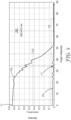
- FIG. 8 shows a plot of optical transmission values versus angle of incidence for an example embodiment of the second optical film 50. Additional discussion of FIG. 8 is presented elsewhere within this specification.
- the first and second optical films may each be constructed from a plurality of layers of polymeric materials.
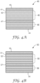
- FIGS. 4A and 4B illustrate embodiments of the first and second optical films, respectively.
- FIG. 4A shows an embodiment of the first optical film 40, including a plurality of alternating first polymeric layers 41 and second polymeric layers 42.
- the combined alternating first 41 and second 42 polymeric layers may number between 100 and 700.
- each first 41 and second 42 polymeric layer may have an average thickness less than about 500 nm, or less than about 400 nm, or less than about 300 nm, or less than about 200 nm, or less than about 100 nm.
- the first 41 and second 42 polymeric layers may have respective indices of refraction, n1x and n2x, along the first polarization state, n1y and n2y along the second polarization state, and n1z and n2z along a z-axis orthogonal to the first and second polarization states, such that for at least one wavelength in the predetermined wavelength range: n1x is greater than each of n1y and n1z by at least 0.2, a difference between n1y and n1z is less than about 0.05, a maximum difference between n2x, n2y and n2z is less than about 0.01, and a difference between n1x and n2x is greater than about 0.2.
- the first optical film 40 may include a top skin layer 43 and a bottom skin layer 44 disposed on opposite top and bottom sides of the plurality of alternating first 41 and second 42 polymeric layers, respectively.
- each skin layer 43/44 may have a thickness greater than about 5 microns.
- the plurality of alternating first 41 and second 42 polymeric layers may be divided into a first plurality 45 of alternating first 41 and second 42 polymeric layers and a second plurality 46 of alternating first 41 and second 42 polymeric layers, where the first plurality 45 and the second plurality 46 are separated from each other by a spacer layer 47 having a thickness greater than about 1 micron.
- FIG. 4B shows an embodiment of the second optical film 50, including a plurality of alternating first polymeric layers 51 and second polymeric layers 52.
- the combined alternating first 51 and second 52 polymeric layers may number between 100 and 700.
- each first 51 and second 52 polymeric layer may have an average thickness less than about 500 nm.
- the first 51 and second 52 polymeric layers may have respective indices of refraction, n1x and n2x, along the first polarization state, n1y and n2y along the second polarization state, and n1z and n2z along a z-axis orthogonal to the first and second polarization states, such that for at least one wavelength in the predetermined wavelength range: each of n1x and n1y is greater than n1z by at least 0.1, a difference between n1x and n1x is less than about 0.05, a maximum difference between n2x, n2y and n2z is less than about 0.01, and a difference between n1x and n2x is greater than about 0.2.
- the second optical film 50 may include a top skin layer 53 and a bottom skin layer 54 disposed on opposite top and bottom sides of the plurality of alternating first 51 and second 52 polymeric layers.
- each skin layer 53/54 may have a thickness greater than about 5 microns.
- the plurality of alternating first 51 and second 52 polymeric layers may be divided into a first plurality 55 of alternating first 51 and second 52 polymeric layers and a second plurality 56 of alternating first 51 and second 52 polymeric layers, where the first plurality 55 and the second plurality 56 are separated from each other by a spacer layer 57 having a thickness greater than about 1 micron.
- FIGS. 5 , 6 , and 7 show the optical transmission percentage values for blue, green, and red wavelengths of light, respectively, at various angles of incidence of an embodiment of the optical stack of the present description.
- FIG. 5 illustrates the transmission of an example optical stack, such as the optical stack of FIG. 1 , for blue wavelengths of light, and specifically for wavelengths extending from about 425 nm to about 475 nm.
- FIG. 6 illustrates the transmission of an example optical stack for green wavelengths of light, and specifically for wavelengths extending from about 525 nm to about 575 nm.
- FIG. 8 illustrates the transmission of an example optical stack for red wavelengths of light, and specifically for wavelengths extending from about 625 nm to about 675 nm.
- the optical stack may have a maximum optical transmittance, T1, for substantially zero incident angle, and an optical transmittance, T1/2, for light incident at less than about 45 degrees for light of the second polarization state, P y .
- T1 for substantially zero incident angle
- T1/2 for light incident at less than about 45 degrees for light of the second polarization state, P y .
- the optical stack has a maximum optical transmittance T2 for incident angles from about zero to about 70 degrees, such that T1/T2 is greater than about 5.
- the ratio of T1/T2 is greater than about 10.
- the optical stack for each wavelength in each of a green wavelength range extending from about 525 nm to about 575 nm ( FIG. 6 ) and a red wavelength range extending from about 625 nm to about 675 nm ( FIG. 7 ) and for each of the first and second polarization states, P x and P y , the optical stack has a maximum optical transmittance (T3 for green wavelengths, FIG. 6 , T4 for red wavelengths, FIG. 7 ) less than a value, TT, for incident angles from about zero degree to about 70 degrees, such that the ratio of maximum optical transmittance, T1, to TT may be greater than about 5. In some embodiments, the ratio of T1/TT may be greater than about 10.
- optical stack 100 may comprise a first optical film 40 and a second optical film 50.
- the second optical film 50 may be a collimating multilayer optical film.
- the second optical film 50 may have an optical transmittance greater than about 80% for substantially zero incident angle, and an optical transmittance less than about 50% for light incident at less than about 45 degrees.
- the second optical film may reflect at least 90% of light for incident angles from about zero degree to about 70 degrees.
- FIG. 8 shows a plot of optical transmission values versus angle of incidence for an example embodiment of the second optical film 50.
- the second optical film 50 has a maximum optical transmittance T max , for light at a first incident angle (e.g., about zero degrees) and an optical transmittance T max /2 at a second incident angle (e.g., about 45 degrees) greater than the first incident angle by less than about 50 degrees.
- substantially aligned will mean aligned to within 20% of a width of the objects being aligned.
- Objects described as substantially aligned may, in some embodiments, be aligned to within 10% or to within 5% of a width of the objects being aligned.
Landscapes
- Physics & Mathematics (AREA)
- Nonlinear Science (AREA)
- General Physics & Mathematics (AREA)
- Optics & Photonics (AREA)
- Mathematical Physics (AREA)
- Chemical & Material Sciences (AREA)
- Crystallography & Structural Chemistry (AREA)
- Liquid Crystal (AREA)
- Polarising Elements (AREA)
- Optical Filters (AREA)
- Planar Illumination Modules (AREA)
Applications Claiming Priority (2)
| Application Number | Priority Date | Filing Date | Title |
|---|---|---|---|
| US201962815468P | 2019-03-08 | 2019-03-08 | |
| PCT/IB2020/051339 WO2020183260A1 (en) | 2019-03-08 | 2020-02-18 | Display optical film and backlight unit |
Publications (2)
| Publication Number | Publication Date |
|---|---|
| EP3935423A1 EP3935423A1 (en) | 2022-01-12 |
| EP3935423B1 true EP3935423B1 (en) | 2024-05-15 |
Family
ID=69740450
Family Applications (1)
| Application Number | Title | Priority Date | Filing Date |
|---|---|---|---|
| EP20708658.8A Active EP3935423B1 (en) | 2019-03-08 | 2020-02-18 | Display optical film and backlight unit |
Country Status (7)
| Country | Link |
|---|---|
| US (3) | US11829024B2 (https=) |
| EP (1) | EP3935423B1 (https=) |
| JP (2) | JP7561750B2 (https=) |
| KR (1) | KR102877519B1 (https=) |
| CN (1) | CN113544553B (https=) |
| TW (1) | TWI888372B (https=) |
| WO (1) | WO2020183260A1 (https=) |
Families Citing this family (3)
| Publication number | Priority date | Publication date | Assignee | Title |
|---|---|---|---|---|
| TWI747575B (zh) * | 2020-10-26 | 2021-11-21 | 南亞塑膠工業股份有限公司 | 具有疊層結構的高分子薄膜 |
| EP4308984A4 (en) * | 2021-03-15 | 2025-07-09 | 3M Innovative Properties Company | MULTILAYER OPTICAL FILM |
| WO2025137080A1 (en) * | 2023-12-20 | 2025-06-26 | Meta Platforms Technologies, Llc | Light collimating film for liquid crystal display backlight |
Family Cites Families (31)
| Publication number | Priority date | Publication date | Assignee | Title |
|---|---|---|---|---|
| KR100344364B1 (ko) * | 1993-12-21 | 2002-11-30 | 미네소타 마이닝 앤드 매뉴팩춰링 캄파니 | 광학편광자및디스플레이장치 |
| EP0962807B1 (en) | 1993-12-21 | 2008-12-03 | Minnesota Mining And Manufacturing Company | Multilayered optical film |
| US6080467A (en) * | 1995-06-26 | 2000-06-27 | 3M Innovative Properties Company | High efficiency optical devices |
| US5808794A (en) * | 1996-07-31 | 1998-09-15 | Weber; Michael F. | Reflective polarizers having extended red band edge for controlled off axis color |
| JP4054623B2 (ja) * | 2002-07-08 | 2008-02-27 | キヤノン株式会社 | 光学多層膜及び光学素子 |
| JP4342821B2 (ja) * | 2003-04-03 | 2009-10-14 | 日東電工株式会社 | 光学素子、液晶セル、照明装置および液晶表示装置 |
| US20040234724A1 (en) | 2003-05-22 | 2004-11-25 | Eastman Kodak Company | Immisible polymer filled optical elements |
| JP2006058332A (ja) * | 2004-08-17 | 2006-03-02 | Seiko Epson Corp | 電気光学装置及び電子機器 |
| US9158155B2 (en) * | 2009-10-24 | 2015-10-13 | 3M Innovative Properties Company | Immersed reflective polarizer with high off-axis reflectivity |
| JP4782864B2 (ja) * | 2009-12-18 | 2011-09-28 | 帝人株式会社 | 1軸延伸多層積層フィルム、それからなる輝度向上用部材、それらからなる液晶ディスプレイ用複合部材およびそれらからなる液晶ディスプレイ装置 |
| JP5782302B2 (ja) | 2011-06-17 | 2015-09-24 | 帝人株式会社 | 多層延伸フィルム |
| KR101792319B1 (ko) * | 2011-10-20 | 2017-10-31 | 데이진 필름 솔루션스 가부시키가이샤 | 1 축 연신 다층 적층 필름 |
| US9488768B2 (en) * | 2011-11-11 | 2016-11-08 | Sumitomo Chemical Company, Limited | Optical film, surface light source device, and liquid crystal display device |
| JP2013250472A (ja) * | 2012-06-01 | 2013-12-12 | Sharp Corp | 表示装置 |
| US9810942B2 (en) * | 2012-06-15 | 2017-11-07 | Apple Inc. | Quantum dot-enhanced display having dichroic filter |
| BR112015019801A2 (pt) * | 2013-02-20 | 2017-07-18 | 3M Innovative Properties Co | pilha de polarizador e luz de fundo |
| CN105378517B (zh) | 2013-06-06 | 2019-04-05 | 富士胶片株式会社 | 光学片部件及使用该光学片部件的图像显示装置 |
| KR20160105442A (ko) * | 2013-12-30 | 2016-09-06 | 쓰리엠 이노베이티브 프로퍼티즈 컴파니 | 시준 반사 편광기를 포함하는 광학 필름 |
| JP2017507373A (ja) * | 2014-03-07 | 2017-03-16 | スリーエム イノベイティブ プロパティズ カンパニー | 多層光学フィルムを組み込む光源 |
| CN106062597B (zh) * | 2014-03-19 | 2019-05-17 | 帝人株式会社 | 液晶显示器偏振片用反射偏振膜、包含其的液晶显示器用偏振片、液晶显示器用光学构件以及液晶显示器 |
| KR101790533B1 (ko) | 2014-12-31 | 2017-10-26 | 도레이케미칼 주식회사 | 반사편광자 및 이를 포함하는 백라이트 유닛 |
| WO2016137777A1 (en) * | 2015-02-27 | 2016-09-01 | 3M Innovative Properties Company | Optical film including collimating reflective polarizer and structured layer |
| US10054734B2 (en) * | 2015-05-08 | 2018-08-21 | Apple Inc. | Liquid crystal display with backlight |
| KR102367295B1 (ko) * | 2015-06-26 | 2022-02-23 | 도레이첨단소재 주식회사 | 반사편광자 및 이를 포함하는 백라이트 유닛 |
| WO2017051867A1 (ja) * | 2015-09-25 | 2017-03-30 | 旭硝子株式会社 | 光学フィルタおよび撮像装置 |
| WO2017087493A1 (en) * | 2015-11-16 | 2017-05-26 | 3M Innovative Properties Company | Display laminate with single packet biaxially birefringent reflective polarizer |
| WO2017175858A1 (ja) * | 2016-04-08 | 2017-10-12 | 富士フイルム株式会社 | 面状光源、バックライトユニット及び液晶表示装置 |
| CN109477924B (zh) * | 2016-07-13 | 2022-02-22 | 3M创新有限公司 | 光学膜 |
| JP6698875B2 (ja) * | 2016-12-21 | 2020-05-27 | 富士フイルム株式会社 | 光学フィルム |
| US10591774B2 (en) * | 2017-04-10 | 2020-03-17 | Apple Inc. | Displays with collimated light sources and quantum dots |
| JP7174929B2 (ja) * | 2017-07-19 | 2022-11-18 | ルムス エルティーディー. | Loeを介するlcos照明 |
-
2020
- 2020-02-18 KR KR1020217032087A patent/KR102877519B1/ko active Active
- 2020-02-18 JP JP2021552989A patent/JP7561750B2/ja active Active
- 2020-02-18 US US17/435,203 patent/US11829024B2/en active Active
- 2020-02-18 WO PCT/IB2020/051339 patent/WO2020183260A1/en not_active Ceased
- 2020-02-18 EP EP20708658.8A patent/EP3935423B1/en active Active
- 2020-02-18 CN CN202080018453.0A patent/CN113544553B/zh active Active
- 2020-03-06 TW TW109107354A patent/TWI888372B/zh active
-
2023
- 2023-10-18 US US18/381,412 patent/US12210241B2/en active Active
-
2024
- 2024-06-04 JP JP2024090351A patent/JP2024119887A/ja not_active Withdrawn
- 2024-12-19 US US18/987,262 patent/US20250123517A1/en active Pending
Also Published As
| Publication number | Publication date |
|---|---|
| US12210241B2 (en) | 2025-01-28 |
| JP2024119887A (ja) | 2024-09-03 |
| US20220137455A1 (en) | 2022-05-05 |
| JP2022523429A (ja) | 2022-04-22 |
| TWI888372B (zh) | 2025-07-01 |
| CN113544553B (zh) | 2023-11-03 |
| JP7561750B2 (ja) | 2024-10-04 |
| US20250123517A1 (en) | 2025-04-17 |
| US20240045261A1 (en) | 2024-02-08 |
| KR20210137125A (ko) | 2021-11-17 |
| EP3935423A1 (en) | 2022-01-12 |
| WO2020183260A1 (en) | 2020-09-17 |
| CN113544553A (zh) | 2021-10-22 |
| KR102877519B1 (ko) | 2025-10-27 |
| TW202109162A (zh) | 2021-03-01 |
| US11829024B2 (en) | 2023-11-28 |
Similar Documents
| Publication | Publication Date | Title |
|---|---|---|
| US12210241B2 (en) | Display optical film and backlight unit | |
| US10168460B2 (en) | Integrated quantum dot optical constructions | |
| JP5877347B2 (ja) | バックライト装置、およびそのバックライト装置を用いた液晶表示装置、およびそれらに用いる発光ダイオード | |
| WO2010137263A1 (ja) | 液晶表示装置 | |
| US12596276B2 (en) | Optical film, backlight and display system | |
| US10663642B2 (en) | Backlight unit, display apparatus including the same and method of manufacturing the same | |
| JP2022523429A5 (https=) | ||
| WO2019127728A1 (zh) | 用于背光模块的量子点膜、背光模块及液晶显示器 | |
| US20140240640A1 (en) | High efficiency polarized and collimated backlight | |
| JP2013250472A (ja) | 表示装置 | |
| US11782310B2 (en) | Backlighting for display systems | |
| KR101904354B1 (ko) | 파장 선택 소자, 광원 장치 및 표시 장치 | |
| KR102423969B1 (ko) | 광학 부재, 이를 포함하는 백라이트 어셈블리 및 액정 표시 장치 | |
| US20230244107A1 (en) | Optical film stack for direct backlight unit | |
| KR102423970B1 (ko) | 광학 부재, 이를 포함하는 백라이트 어셈블리 및 액정 표시 장치 | |
| KR20170042964A (ko) | 광원 유닛 및 이를 이용한 표시 장치 | |
| WO2025040976A1 (en) | Backlight and display system | |
| EP4652628A1 (en) | Display system with reduced crosstalk contamination | |
| KR20170134190A (ko) | 액정 표시 장치, 광원 장치 및 광원 장치의 제조 방법 |
Legal Events
| Date | Code | Title | Description |
|---|---|---|---|
| STAA | Information on the status of an ep patent application or granted ep patent |
Free format text: STATUS: UNKNOWN |
|
| STAA | Information on the status of an ep patent application or granted ep patent |
Free format text: STATUS: THE INTERNATIONAL PUBLICATION HAS BEEN MADE |
|
| PUAI | Public reference made under article 153(3) epc to a published international application that has entered the european phase |
Free format text: ORIGINAL CODE: 0009012 |
|
| STAA | Information on the status of an ep patent application or granted ep patent |
Free format text: STATUS: REQUEST FOR EXAMINATION WAS MADE |
|
| 17P | Request for examination filed |
Effective date: 20210902 |
|
| AK | Designated contracting states |
Kind code of ref document: A1 Designated state(s): AL AT BE BG CH CY CZ DE DK EE ES FI FR GB GR HR HU IE IS IT LI LT LU LV MC MK MT NL NO PL PT RO RS SE SI SK SM TR |
|
| DAV | Request for validation of the european patent (deleted) | ||
| DAX | Request for extension of the european patent (deleted) | ||
| REG | Reference to a national code |
Ref country code: DE Ref legal event code: R079 Free format text: PREVIOUS MAIN CLASS: G02B0005300000 Ipc: G02F0001133570 Ref country code: DE Ref legal event code: R079 Ref document number: 602020030909 Country of ref document: DE Free format text: PREVIOUS MAIN CLASS: G02B0005300000 Ipc: G02F0001133570 |
|
| GRAP | Despatch of communication of intention to grant a patent |
Free format text: ORIGINAL CODE: EPIDOSNIGR1 |
|
| STAA | Information on the status of an ep patent application or granted ep patent |
Free format text: STATUS: GRANT OF PATENT IS INTENDED |
|
| RIC1 | Information provided on ipc code assigned before grant |
Ipc: G02F 1/1335 20060101ALI20231117BHEP Ipc: G02B 5/30 20060101ALI20231117BHEP Ipc: G02F 1/13357 20060101AFI20231117BHEP |
|
| INTG | Intention to grant announced |
Effective date: 20231213 |
|
| P01 | Opt-out of the competence of the unified patent court (upc) registered |
Effective date: 20240226 |
|
| GRAS | Grant fee paid |
Free format text: ORIGINAL CODE: EPIDOSNIGR3 |
|
| GRAA | (expected) grant |
Free format text: ORIGINAL CODE: 0009210 |
|
| STAA | Information on the status of an ep patent application or granted ep patent |
Free format text: STATUS: THE PATENT HAS BEEN GRANTED |
|
| AK | Designated contracting states |
Kind code of ref document: B1 Designated state(s): AL AT BE BG CH CY CZ DE DK EE ES FI FR GB GR HR HU IE IS IT LI LT LU LV MC MK MT NL NO PL PT RO RS SE SI SK SM TR |
|
| REG | Reference to a national code |
Ref country code: CH Ref legal event code: EP |
|
| REG | Reference to a national code |
Ref country code: IE Ref legal event code: FG4D |
|
| REG | Reference to a national code |
Ref country code: DE Ref legal event code: R096 Ref document number: 602020030909 Country of ref document: DE |
|
| REG | Reference to a national code |
Ref country code: LT Ref legal event code: MG9D |
|
| REG | Reference to a national code |
Ref country code: NL Ref legal event code: MP Effective date: 20240515 |
|
| PG25 | Lapsed in a contracting state [announced via postgrant information from national office to epo] |
Ref country code: IS Free format text: LAPSE BECAUSE OF FAILURE TO SUBMIT A TRANSLATION OF THE DESCRIPTION OR TO PAY THE FEE WITHIN THE PRESCRIBED TIME-LIMIT Effective date: 20240915 |
|
| PG25 | Lapsed in a contracting state [announced via postgrant information from national office to epo] |
Ref country code: BG Free format text: LAPSE BECAUSE OF FAILURE TO SUBMIT A TRANSLATION OF THE DESCRIPTION OR TO PAY THE FEE WITHIN THE PRESCRIBED TIME-LIMIT Effective date: 20240515 |
|
| PG25 | Lapsed in a contracting state [announced via postgrant information from national office to epo] |
Ref country code: HR Free format text: LAPSE BECAUSE OF FAILURE TO SUBMIT A TRANSLATION OF THE DESCRIPTION OR TO PAY THE FEE WITHIN THE PRESCRIBED TIME-LIMIT Effective date: 20240515 Ref country code: FI Free format text: LAPSE BECAUSE OF FAILURE TO SUBMIT A TRANSLATION OF THE DESCRIPTION OR TO PAY THE FEE WITHIN THE PRESCRIBED TIME-LIMIT Effective date: 20240515 |
|
| PG25 | Lapsed in a contracting state [announced via postgrant information from national office to epo] |
Ref country code: GR Free format text: LAPSE BECAUSE OF FAILURE TO SUBMIT A TRANSLATION OF THE DESCRIPTION OR TO PAY THE FEE WITHIN THE PRESCRIBED TIME-LIMIT Effective date: 20240816 |
|
| PG25 | Lapsed in a contracting state [announced via postgrant information from national office to epo] |
Ref country code: PT Free format text: LAPSE BECAUSE OF FAILURE TO SUBMIT A TRANSLATION OF THE DESCRIPTION OR TO PAY THE FEE WITHIN THE PRESCRIBED TIME-LIMIT Effective date: 20240916 |
|
| REG | Reference to a national code |
Ref country code: AT Ref legal event code: MK05 Ref document number: 1687376 Country of ref document: AT Kind code of ref document: T Effective date: 20240515 |
|
| PG25 | Lapsed in a contracting state [announced via postgrant information from national office to epo] |
Ref country code: NL Free format text: LAPSE BECAUSE OF FAILURE TO SUBMIT A TRANSLATION OF THE DESCRIPTION OR TO PAY THE FEE WITHIN THE PRESCRIBED TIME-LIMIT Effective date: 20240515 |
|
| PG25 | Lapsed in a contracting state [announced via postgrant information from national office to epo] |
Ref country code: ES Free format text: LAPSE BECAUSE OF FAILURE TO SUBMIT A TRANSLATION OF THE DESCRIPTION OR TO PAY THE FEE WITHIN THE PRESCRIBED TIME-LIMIT Effective date: 20240515 |
|
| PG25 | Lapsed in a contracting state [announced via postgrant information from national office to epo] |
Ref country code: AT Free format text: LAPSE BECAUSE OF FAILURE TO SUBMIT A TRANSLATION OF THE DESCRIPTION OR TO PAY THE FEE WITHIN THE PRESCRIBED TIME-LIMIT Effective date: 20240515 |
|
| PG25 | Lapsed in a contracting state [announced via postgrant information from national office to epo] |
Ref country code: PL Free format text: LAPSE BECAUSE OF FAILURE TO SUBMIT A TRANSLATION OF THE DESCRIPTION OR TO PAY THE FEE WITHIN THE PRESCRIBED TIME-LIMIT Effective date: 20240515 |
|
| PG25 | Lapsed in a contracting state [announced via postgrant information from national office to epo] |
Ref country code: LV Free format text: LAPSE BECAUSE OF FAILURE TO SUBMIT A TRANSLATION OF THE DESCRIPTION OR TO PAY THE FEE WITHIN THE PRESCRIBED TIME-LIMIT Effective date: 20240515 |
|
| PG25 | Lapsed in a contracting state [announced via postgrant information from national office to epo] |
Ref country code: PT Free format text: LAPSE BECAUSE OF FAILURE TO SUBMIT A TRANSLATION OF THE DESCRIPTION OR TO PAY THE FEE WITHIN THE PRESCRIBED TIME-LIMIT Effective date: 20240916 Ref country code: PL Free format text: LAPSE BECAUSE OF FAILURE TO SUBMIT A TRANSLATION OF THE DESCRIPTION OR TO PAY THE FEE WITHIN THE PRESCRIBED TIME-LIMIT Effective date: 20240515 Ref country code: NO Free format text: LAPSE BECAUSE OF FAILURE TO SUBMIT A TRANSLATION OF THE DESCRIPTION OR TO PAY THE FEE WITHIN THE PRESCRIBED TIME-LIMIT Effective date: 20240815 Ref country code: NL Free format text: LAPSE BECAUSE OF FAILURE TO SUBMIT A TRANSLATION OF THE DESCRIPTION OR TO PAY THE FEE WITHIN THE PRESCRIBED TIME-LIMIT Effective date: 20240515 Ref country code: LV Free format text: LAPSE BECAUSE OF FAILURE TO SUBMIT A TRANSLATION OF THE DESCRIPTION OR TO PAY THE FEE WITHIN THE PRESCRIBED TIME-LIMIT Effective date: 20240515 Ref country code: IS Free format text: LAPSE BECAUSE OF FAILURE TO SUBMIT A TRANSLATION OF THE DESCRIPTION OR TO PAY THE FEE WITHIN THE PRESCRIBED TIME-LIMIT Effective date: 20240915 Ref country code: HR Free format text: LAPSE BECAUSE OF FAILURE TO SUBMIT A TRANSLATION OF THE DESCRIPTION OR TO PAY THE FEE WITHIN THE PRESCRIBED TIME-LIMIT Effective date: 20240515 Ref country code: GR Free format text: LAPSE BECAUSE OF FAILURE TO SUBMIT A TRANSLATION OF THE DESCRIPTION OR TO PAY THE FEE WITHIN THE PRESCRIBED TIME-LIMIT Effective date: 20240816 Ref country code: FI Free format text: LAPSE BECAUSE OF FAILURE TO SUBMIT A TRANSLATION OF THE DESCRIPTION OR TO PAY THE FEE WITHIN THE PRESCRIBED TIME-LIMIT Effective date: 20240515 Ref country code: ES Free format text: LAPSE BECAUSE OF FAILURE TO SUBMIT A TRANSLATION OF THE DESCRIPTION OR TO PAY THE FEE WITHIN THE PRESCRIBED TIME-LIMIT Effective date: 20240515 Ref country code: BG Free format text: LAPSE BECAUSE OF FAILURE TO SUBMIT A TRANSLATION OF THE DESCRIPTION OR TO PAY THE FEE WITHIN THE PRESCRIBED TIME-LIMIT Effective date: 20240515 Ref country code: AT Free format text: LAPSE BECAUSE OF FAILURE TO SUBMIT A TRANSLATION OF THE DESCRIPTION OR TO PAY THE FEE WITHIN THE PRESCRIBED TIME-LIMIT Effective date: 20240515 Ref country code: RS Free format text: LAPSE BECAUSE OF FAILURE TO SUBMIT A TRANSLATION OF THE DESCRIPTION OR TO PAY THE FEE WITHIN THE PRESCRIBED TIME-LIMIT Effective date: 20240815 |
|
| PG25 | Lapsed in a contracting state [announced via postgrant information from national office to epo] |
Ref country code: DK Free format text: LAPSE BECAUSE OF FAILURE TO SUBMIT A TRANSLATION OF THE DESCRIPTION OR TO PAY THE FEE WITHIN THE PRESCRIBED TIME-LIMIT Effective date: 20240515 |
|
| PG25 | Lapsed in a contracting state [announced via postgrant information from national office to epo] |
Ref country code: EE Free format text: LAPSE BECAUSE OF FAILURE TO SUBMIT A TRANSLATION OF THE DESCRIPTION OR TO PAY THE FEE WITHIN THE PRESCRIBED TIME-LIMIT Effective date: 20240515 |
|
| PG25 | Lapsed in a contracting state [announced via postgrant information from national office to epo] |
Ref country code: CZ Free format text: LAPSE BECAUSE OF FAILURE TO SUBMIT A TRANSLATION OF THE DESCRIPTION OR TO PAY THE FEE WITHIN THE PRESCRIBED TIME-LIMIT Effective date: 20240515 |
|
| PG25 | Lapsed in a contracting state [announced via postgrant information from national office to epo] |
Ref country code: RO Free format text: LAPSE BECAUSE OF FAILURE TO SUBMIT A TRANSLATION OF THE DESCRIPTION OR TO PAY THE FEE WITHIN THE PRESCRIBED TIME-LIMIT Effective date: 20240515 Ref country code: SK Free format text: LAPSE BECAUSE OF FAILURE TO SUBMIT A TRANSLATION OF THE DESCRIPTION OR TO PAY THE FEE WITHIN THE PRESCRIBED TIME-LIMIT Effective date: 20240515 |
|
| PG25 | Lapsed in a contracting state [announced via postgrant information from national office to epo] |
Ref country code: SM Free format text: LAPSE BECAUSE OF FAILURE TO SUBMIT A TRANSLATION OF THE DESCRIPTION OR TO PAY THE FEE WITHIN THE PRESCRIBED TIME-LIMIT Effective date: 20240515 |
|
| PG25 | Lapsed in a contracting state [announced via postgrant information from national office to epo] |
Ref country code: SM Free format text: LAPSE BECAUSE OF FAILURE TO SUBMIT A TRANSLATION OF THE DESCRIPTION OR TO PAY THE FEE WITHIN THE PRESCRIBED TIME-LIMIT Effective date: 20240515 Ref country code: SK Free format text: LAPSE BECAUSE OF FAILURE TO SUBMIT A TRANSLATION OF THE DESCRIPTION OR TO PAY THE FEE WITHIN THE PRESCRIBED TIME-LIMIT Effective date: 20240515 Ref country code: RO Free format text: LAPSE BECAUSE OF FAILURE TO SUBMIT A TRANSLATION OF THE DESCRIPTION OR TO PAY THE FEE WITHIN THE PRESCRIBED TIME-LIMIT Effective date: 20240515 Ref country code: EE Free format text: LAPSE BECAUSE OF FAILURE TO SUBMIT A TRANSLATION OF THE DESCRIPTION OR TO PAY THE FEE WITHIN THE PRESCRIBED TIME-LIMIT Effective date: 20240515 Ref country code: DK Free format text: LAPSE BECAUSE OF FAILURE TO SUBMIT A TRANSLATION OF THE DESCRIPTION OR TO PAY THE FEE WITHIN THE PRESCRIBED TIME-LIMIT Effective date: 20240515 Ref country code: CZ Free format text: LAPSE BECAUSE OF FAILURE TO SUBMIT A TRANSLATION OF THE DESCRIPTION OR TO PAY THE FEE WITHIN THE PRESCRIBED TIME-LIMIT Effective date: 20240515 |
|
| PG25 | Lapsed in a contracting state [announced via postgrant information from national office to epo] |
Ref country code: IT Free format text: LAPSE BECAUSE OF FAILURE TO SUBMIT A TRANSLATION OF THE DESCRIPTION OR TO PAY THE FEE WITHIN THE PRESCRIBED TIME-LIMIT Effective date: 20240515 |
|
| REG | Reference to a national code |
Ref country code: DE Ref legal event code: R097 Ref document number: 602020030909 Country of ref document: DE |
|
| PLBE | No opposition filed within time limit |
Free format text: ORIGINAL CODE: 0009261 |
|
| STAA | Information on the status of an ep patent application or granted ep patent |
Free format text: STATUS: NO OPPOSITION FILED WITHIN TIME LIMIT |
|
| 26N | No opposition filed |
Effective date: 20250218 |
|
| PG25 | Lapsed in a contracting state [announced via postgrant information from national office to epo] |
Ref country code: SI Free format text: LAPSE BECAUSE OF FAILURE TO SUBMIT A TRANSLATION OF THE DESCRIPTION OR TO PAY THE FEE WITHIN THE PRESCRIBED TIME-LIMIT Effective date: 20240515 |
|
| PG25 | Lapsed in a contracting state [announced via postgrant information from national office to epo] |
Ref country code: SE Free format text: LAPSE BECAUSE OF FAILURE TO SUBMIT A TRANSLATION OF THE DESCRIPTION OR TO PAY THE FEE WITHIN THE PRESCRIBED TIME-LIMIT Effective date: 20240515 |
|
| PG25 | Lapsed in a contracting state [announced via postgrant information from national office to epo] |
Ref country code: MC Free format text: LAPSE BECAUSE OF FAILURE TO SUBMIT A TRANSLATION OF THE DESCRIPTION OR TO PAY THE FEE WITHIN THE PRESCRIBED TIME-LIMIT Effective date: 20240515 |
|
| REG | Reference to a national code |
Ref country code: CH Ref legal event code: PL |
|
| PG25 | Lapsed in a contracting state [announced via postgrant information from national office to epo] |
Ref country code: LU Free format text: LAPSE BECAUSE OF NON-PAYMENT OF DUE FEES Effective date: 20250218 |
|
| PG25 | Lapsed in a contracting state [announced via postgrant information from national office to epo] |
Ref country code: CH Free format text: LAPSE BECAUSE OF NON-PAYMENT OF DUE FEES Effective date: 20250228 |
|
| GBPC | Gb: european patent ceased through non-payment of renewal fee |
Effective date: 20250218 |
|
| REG | Reference to a national code |
Ref country code: BE Ref legal event code: MM Effective date: 20250228 |
|
| PG25 | Lapsed in a contracting state [announced via postgrant information from national office to epo] |
Ref country code: GB Free format text: LAPSE BECAUSE OF NON-PAYMENT OF DUE FEES Effective date: 20250218 |
|
| PG25 | Lapsed in a contracting state [announced via postgrant information from national office to epo] |
Ref country code: FR Free format text: LAPSE BECAUSE OF NON-PAYMENT OF DUE FEES Effective date: 20250228 |
|
| PG25 | Lapsed in a contracting state [announced via postgrant information from national office to epo] |
Ref country code: BE Free format text: LAPSE BECAUSE OF NON-PAYMENT OF DUE FEES Effective date: 20250228 |
|
| PG25 | Lapsed in a contracting state [announced via postgrant information from national office to epo] |
Ref country code: IE Free format text: LAPSE BECAUSE OF NON-PAYMENT OF DUE FEES Effective date: 20250218 |
|
| PGFP | Annual fee paid to national office [announced via postgrant information from national office to epo] |
Ref country code: DE Payment date: 20260121 Year of fee payment: 7 |