EP3929905B1 - Schieberegistereinheit, gate-ansteuerungsvorrichtung, anzeigevorrichtung und ansteuerungsverfahren - Google Patents
Schieberegistereinheit, gate-ansteuerungsvorrichtung, anzeigevorrichtung und ansteuerungsverfahren Download PDFInfo
- Publication number
- EP3929905B1 EP3929905B1 EP20759878.0A EP20759878A EP3929905B1 EP 3929905 B1 EP3929905 B1 EP 3929905B1 EP 20759878 A EP20759878 A EP 20759878A EP 3929905 B1 EP3929905 B1 EP 3929905B1
- Authority
- EP
- European Patent Office
- Prior art keywords
- node
- transistor
- circuit
- electrode
- shift register
- Prior art date
- Legal status (The legal status is an assumption and is not a legal conclusion. Google has not performed a legal analysis and makes no representation as to the accuracy of the status listed.)
- Active
Links
Images


Classifications
-
- G—PHYSICS
- G09—EDUCATION; CRYPTOGRAPHY; DISPLAY; ADVERTISING; SEALS
- G09G—ARRANGEMENTS OR CIRCUITS FOR CONTROL OF INDICATING DEVICES USING STATIC MEANS TO PRESENT VARIABLE INFORMATION
- G09G3/00—Control arrangements or circuits, of interest only in connection with visual indicators other than cathode-ray tubes
- G09G3/20—Control arrangements or circuits, of interest only in connection with visual indicators other than cathode-ray tubes for presentation of an assembly of a number of characters, e.g. a page, by composing the assembly by combination of individual elements arranged in a matrix no fixed position being assigned to or needed to be assigned to the individual characters or partial characters
- G09G3/22—Control arrangements or circuits, of interest only in connection with visual indicators other than cathode-ray tubes for presentation of an assembly of a number of characters, e.g. a page, by composing the assembly by combination of individual elements arranged in a matrix no fixed position being assigned to or needed to be assigned to the individual characters or partial characters using controlled light sources
- G09G3/30—Control arrangements or circuits, of interest only in connection with visual indicators other than cathode-ray tubes for presentation of an assembly of a number of characters, e.g. a page, by composing the assembly by combination of individual elements arranged in a matrix no fixed position being assigned to or needed to be assigned to the individual characters or partial characters using controlled light sources using electroluminescent panels
- G09G3/32—Control arrangements or circuits, of interest only in connection with visual indicators other than cathode-ray tubes for presentation of an assembly of a number of characters, e.g. a page, by composing the assembly by combination of individual elements arranged in a matrix no fixed position being assigned to or needed to be assigned to the individual characters or partial characters using controlled light sources using electroluminescent panels semiconductive, e.g. using light-emitting diodes [LED]
- G09G3/3208—Control arrangements or circuits, of interest only in connection with visual indicators other than cathode-ray tubes for presentation of an assembly of a number of characters, e.g. a page, by composing the assembly by combination of individual elements arranged in a matrix no fixed position being assigned to or needed to be assigned to the individual characters or partial characters using controlled light sources using electroluminescent panels semiconductive, e.g. using light-emitting diodes [LED] organic, e.g. using organic light-emitting diodes [OLED]
- G09G3/3225—Control arrangements or circuits, of interest only in connection with visual indicators other than cathode-ray tubes for presentation of an assembly of a number of characters, e.g. a page, by composing the assembly by combination of individual elements arranged in a matrix no fixed position being assigned to or needed to be assigned to the individual characters or partial characters using controlled light sources using electroluminescent panels semiconductive, e.g. using light-emitting diodes [LED] organic, e.g. using organic light-emitting diodes [OLED] using an active matrix
-
- G—PHYSICS
- G09—EDUCATION; CRYPTOGRAPHY; DISPLAY; ADVERTISING; SEALS
- G09G—ARRANGEMENTS OR CIRCUITS FOR CONTROL OF INDICATING DEVICES USING STATIC MEANS TO PRESENT VARIABLE INFORMATION
- G09G3/00—Control arrangements or circuits, of interest only in connection with visual indicators other than cathode-ray tubes
- G09G3/20—Control arrangements or circuits, of interest only in connection with visual indicators other than cathode-ray tubes for presentation of an assembly of a number of characters, e.g. a page, by composing the assembly by combination of individual elements arranged in a matrix no fixed position being assigned to or needed to be assigned to the individual characters or partial characters
- G09G3/22—Control arrangements or circuits, of interest only in connection with visual indicators other than cathode-ray tubes for presentation of an assembly of a number of characters, e.g. a page, by composing the assembly by combination of individual elements arranged in a matrix no fixed position being assigned to or needed to be assigned to the individual characters or partial characters using controlled light sources
- G09G3/30—Control arrangements or circuits, of interest only in connection with visual indicators other than cathode-ray tubes for presentation of an assembly of a number of characters, e.g. a page, by composing the assembly by combination of individual elements arranged in a matrix no fixed position being assigned to or needed to be assigned to the individual characters or partial characters using controlled light sources using electroluminescent panels
- G09G3/32—Control arrangements or circuits, of interest only in connection with visual indicators other than cathode-ray tubes for presentation of an assembly of a number of characters, e.g. a page, by composing the assembly by combination of individual elements arranged in a matrix no fixed position being assigned to or needed to be assigned to the individual characters or partial characters using controlled light sources using electroluminescent panels semiconductive, e.g. using light-emitting diodes [LED]
- G09G3/3208—Control arrangements or circuits, of interest only in connection with visual indicators other than cathode-ray tubes for presentation of an assembly of a number of characters, e.g. a page, by composing the assembly by combination of individual elements arranged in a matrix no fixed position being assigned to or needed to be assigned to the individual characters or partial characters using controlled light sources using electroluminescent panels semiconductive, e.g. using light-emitting diodes [LED] organic, e.g. using organic light-emitting diodes [OLED]
- G09G3/3266—Details of drivers for scan electrodes
-
- G—PHYSICS
- G11—INFORMATION STORAGE
- G11C—STATIC STORES
- G11C19/00—Digital stores in which the information is moved stepwise, e.g. shift registers
- G11C19/28—Digital stores in which the information is moved stepwise, e.g. shift registers using semiconductor elements
-
- G—PHYSICS
- G09—EDUCATION; CRYPTOGRAPHY; DISPLAY; ADVERTISING; SEALS
- G09G—ARRANGEMENTS OR CIRCUITS FOR CONTROL OF INDICATING DEVICES USING STATIC MEANS TO PRESENT VARIABLE INFORMATION
- G09G2300/00—Aspects of the constitution of display devices
- G09G2300/04—Structural and physical details of display devices
- G09G2300/0421—Structural details of the set of electrodes
- G09G2300/0426—Layout of electrodes and connections
-
- G—PHYSICS
- G09—EDUCATION; CRYPTOGRAPHY; DISPLAY; ADVERTISING; SEALS
- G09G—ARRANGEMENTS OR CIRCUITS FOR CONTROL OF INDICATING DEVICES USING STATIC MEANS TO PRESENT VARIABLE INFORMATION
- G09G2310/00—Command of the display device
- G09G2310/02—Addressing, scanning or driving the display screen or processing steps related thereto
- G09G2310/0264—Details of driving circuits
- G09G2310/0286—Details of a shift registers arranged for use in a driving circuit
-
- G—PHYSICS
- G09—EDUCATION; CRYPTOGRAPHY; DISPLAY; ADVERTISING; SEALS
- G09G—ARRANGEMENTS OR CIRCUITS FOR CONTROL OF INDICATING DEVICES USING STATIC MEANS TO PRESENT VARIABLE INFORMATION
- G09G2310/00—Command of the display device
- G09G2310/06—Details of flat display driving waveforms
- G09G2310/061—Details of flat display driving waveforms for resetting or blanking
-
- G—PHYSICS
- G09—EDUCATION; CRYPTOGRAPHY; DISPLAY; ADVERTISING; SEALS
- G09G—ARRANGEMENTS OR CIRCUITS FOR CONTROL OF INDICATING DEVICES USING STATIC MEANS TO PRESENT VARIABLE INFORMATION
- G09G2310/00—Command of the display device
- G09G2310/08—Details of timing specific for flat panels, other than clock recovery
-
- G—PHYSICS
- G09—EDUCATION; CRYPTOGRAPHY; DISPLAY; ADVERTISING; SEALS
- G09G—ARRANGEMENTS OR CIRCUITS FOR CONTROL OF INDICATING DEVICES USING STATIC MEANS TO PRESENT VARIABLE INFORMATION
- G09G2320/00—Control of display operating conditions
- G09G2320/02—Improving the quality of display appearance
- G09G2320/0233—Improving the luminance or brightness uniformity across the screen
Definitions
- the embodiments of the present disclosure relate to a shift register unit, a gate driving circuit, a display device, and a driving method.
- gate driving circuits are generally integrated in gate driving chips (GATE ICs) currently.
- GATE ICs gate driving chips
- the area of a chip is a main factor that affects the cost of the chip, so how to effectively reduce the area of the chip is what technology developers need to focus on.
- US2021/201805A1 discloses an electronic panel, a display device and a driving method.
- each row of subpixel units is divided into a plurality of subpixel unit groups, and each subpixel unit group includes a first subpixel unit and a second subpixel unit.
- the first subpixel unit includes a first light emitter unit, a first pixel driving circuit for driving the first light emitter unit to emit light, and a first sensing circuit for sensing the first pixel driving circuit;
- the second subpixel unit includes a second light emitter unit, a second pixel driving circuit for driving the second light emitter unit to emit light, and a second sensing circuit for sensing the second pixel driving circuit.
- US2020/143766A1 discloses a shift register comprising an input sub-circuit, an output sub-circuit, a pull-down control sub-circuit, a pull-down sub-circuit, a first reset sub-circuit and a second reset sub-circuit.
- the first reset sub-circuit is electrically coupled to the input sub-circuit, and the second reset sub-circuit and the output sub-circuit are both electrically coupled to a signal output terminal.
- US 2020/356203A1 discloses a shift register unit, a method of driving a shift register unit, a gate driving circuit and a touch display device, which can solve a problem that the output voltage of the output transistor of a shift register unit is insufficient.
- the shift register unit comprises an anti-leakage circuit, which is configured to bring a first node into conduction with a second node in response to an active potential of the second voltage terminal.
- connection is not intended to define a physical connection or mechanical connection, but may include an electrical connection, directly or indirectly.
- "On,” “under,” “right,” “left” and the like are only used to indicate relative position relationship, and when the position of the object which is described is changed, the relative position relationship may be changed accordingly.
- the term "pull up” means to charge a node or an electrode of a transistor to increase the absolute value of the level of the node or the electrode, so as to achieve the operation (for example, turning on) of the corresponding transistor; and the term “pull down” means to discharge a node or an electrode of a transistor to reduce the absolute value of the level of the node or the electrode, so as to achieve the operation (for example, turning off) of the corresponding transistor.
- the term "pull up” means to discharge a node or an electrode of a transistor to reduce the absolute value of the level of the node or the electrode, so as to achieve the operation (for example, turning on) of the corresponding transistor; and the term “pull down” means to charge a node or an electrode of a transistor to increase the absolute value of the level of the node or the electrode, so as to achieve the operation (for example, turning off) of the corresponding transistor.
- a gate driving circuit for an OLED usually includes three sub-circuits, i.e., a detection circuit, a display circuit, and a connection circuit (or a gate circuit) that outputs a composite pulse of the detection circuit and the display circuit.
- a detection circuit i.e., a detection circuit
- a display circuit i.e., a display circuit
- a connection circuit or a gate circuit
- Such circuit structure is very complicated and cannot meet requirements of a high resolution and a narrow bezel of a display panel.
- a gate driving circuit including shift register units needs to provide driving signals for a scanning transistor and a sensing transistor respectively to the sub-pixel unit in the display panel, for example, a scanning driving signal for the scanning transistor in a display period of a frame and a sensing driving signal for the sensing transistor in a blanking period of a frame.
- the sensing driving signal output by the gate driving circuit is used for progressive sequential scanning. For example, during a blanking period of a first frame, a sensing driving signal for a first row of sub-pixel units in the display panel is output, and during a blanking period of a second frame, a sensing driving signal for a second row of sub-pixel units in the display panel is output, and so on.
- the sensing driving signals are sequentially outputted row by row at a frequency which is outputting the sensing driving signal of a corresponding row of sub-pixel units during each frame, and thus the progressive sequential compensation of the display panel is completed.
- the gate driving circuit when a gate driving circuit drives a display panel, if external compensation is to be realized, the gate driving circuit needs to not only output the scanning driving signal for the display period, but also output the sensing driving signal for the blanking period.
- a level of a control terminal (for example, connected to a first node) of a output circuit in the shift register unit needs to be maintained at a high level; for another example, in the case where the shift register unit is not required to output the driving signal, a level of the first node needs to be maintained at a low level; in other words, the level of the first node directly affects the output of the shift register unit, the level of the first node should be stably maintained at a low level in a non-output stage, otherwise the shift register unit may output signals multiple times within a frame.
- a control circuit and a reset circuit are generally provided in the shift register unit.
- the control circuit is configured to control a level of a second node
- the reset circuit is configured to control the level of the first node under the control of the level of the second node.
- the level of the second node needs to be maintained at a high level. In the non-output stage, if the level of the second node fails to be maintained at a high level, it may cause the level of the first node to drift, thereby affecting the normal output of the shift register unit.
- At least one embodiment of the present disclosure provides a shift register unit including a first input circuit, an output circuit, a first control circuit, a first reset circuit, a second input circuit, a transmission circuit, and a storage circuit.
- the first input circuit is configured to control a level of a first node in response to a first input signal
- the output circuit is configured to provide an output signal at an output terminal under the control of the level of the first node
- the first control circuit is configured to control a level of a second node under the control of the level of the first node
- the first reset circuit is configured to reset the first node and the output terminal under the control of the level of the second node
- the second input circuit is configured to control a level of a third node in response to a selection control signal
- the transmission circuit is configured to control the level of the first node according to the level of the third node
- the storage circuit is electrically connected to the second node, and is configured to stabilize the level of the second node.
- Embodiments of the present disclosure also provide a gate driving circuit, a display device, and a driving method corresponding to the above shift register unit.
- the shift register unit, the gate driving circuit, the display device, and the driving method provided by the embodiments of the present disclosure can better stabilize the level of the second node in the shift register unit.
- the second node in a stage where the shift register unit does not need to output a driving signal (an non-output stage), the second node can be stably maintained at a high level, so that the level of the first node does not drift and is stably maintained at a low level, thereby preventing the shift register unit from outputting signals multiple times.
- the corresponding gate driving circuit and the display device can also realize random compensation, thereby avoiding the problems of poor display effects such as scanning lines and uneven display brightness caused by the progressive sequential compensation.
- the random compensation refers to an external compensation method that is different from the progressive sequential compensation, which can randomly output a sensing driving signal corresponding to any row of sub-pixel units in the display panel during a blanking period of a frame.
- the same explanation also applies to following embodiments, and will not be described in detail.
- a frame is defined to include a display period and a blanking period sequentially occur, for example, during the display period, the gate driving circuit outputs a driving signal, which can drive the display panel to complete the scanning display of a whole image from the first row to the last row, and during the blanking period, the gate driving circuit outputs a driving signal, which can be used to drive a sensing transistor in a row of sub-pixel units in the display panel to complete external compensation of the row of sub-pixel units.
- FIG. 1 is a schematic diagram of a shift register unit provided by some embodiments of the present disclosure
- FIG. 2 is a schematic diagram of another shift register unit provided by some embodiments of the present disclosure.
- the shift register unit 10 includes a first input circuit 110, an output circuit 120, a first control circuit 130, and a first reset circuit 140, a second input circuit 150, a transmission circuit 160, and a storage circuit 170.
- a plurality of the shift register units 10 can be cascaded to construct a gate driving circuit provided by an embodiment of the present disclosure, and the gate driving circuit can be used in a display device to provide a driving signal during the displaying process of a frame of the display device.
- the first input circuit 110 is configured to control a level of a first node Q in response to a first input signal STU1, for example, to charge the first node Q.
- the first input circuit 110 may be configured to receive the first input signal STU1 and a second voltage VDD, and the first input circuit 110 is turned on in response to the first input signal STU1, so that the first node Q1 can be charged with the second voltage VDD.
- the first input circuit 110 may also not receive the second voltage VDD, and directly charges the first node Q1 with the first input signal STU1.
- the second voltage VDD is, for example, a high level.
- the same case also applies to the following embodiments, and will not be repeated.
- the output circuit 120 is configured to provide an output signal at an output terminal OP under the control of the level of the first node Q.
- the output terminal OP includes a shifting signal output terminal CRT and a driving signal output terminal DST, and accordingly, the output signals include a shifting signal CR and a driving signal OUT.
- the output circuit 120 may be configured to receive a third clock signal CLKC, and when being turned on under the control of the level of the first node Q, the output circuit 120 may provide the third clock signal CLKC to the shifting signal output terminal CRT as the shifting signal CR, and provide the third clock signal CLKC to the driving signal output terminal DST as the driving signal OUT.
- the shifting signal CR output by the output circuit 120 may be provided to other shift register units 10 as the first input signal STU1, thereby completing the progressive shift of the display scan; the driving signal OUT output by the output circuit 120 can drive a row of sub-pixel units in the display panel to perform the display scan.
- some of the shift register units 10 can be connected to a clock signal line to receive the first input signals STU1 provided by the clock signal line; alternatively, some of shift register units 10 may also receive the shifting signals CR output by other shift register units 10 as the first input signals STU1.
- the signal waveforms of the shifting signal CR and the driving signal OUT output by the output circuit 120 may be the same or different, which is not limited in the embodiments of the present disclosure.
- the first control circuit 130 is configured to control a level of a second node QB under the control of the level of the first node Q.
- the first control circuit 130 is connected to the first node Q and the second node QB, and is configured to receive a first voltage VGL1 and the second voltage VDD.
- the first control circuit 130 may pull down the second node QB to a low level with the first voltage VGL1 at a low level.
- the first control circuit 130 is configured to receive a second clock signal CLKB, and in the case where the first node Q is at a low level and the second clock signal CLKB is at a high level, the first control circuit 130 can be turned on in response to the second clock signal CLKB at a high level, so that the second node QB can be charged with the second voltage VDD at a high level to pull up the second node QB to a high level.
- the first voltage VGL1 is, for example, a low level.
- the following embodiments are the same as this, and will not be described in detail.
- the first reset circuit 140 is configured to reset the first node Q and the output terminal OP (for example, including the shifting signal output terminal CRT and the driving signal output terminal DST) under the control of the level of the second node QB.
- the first reset circuit 140 is connected to the first node Q, the second node QB, and the output terminal OP, and is configured to receive the first voltage VGL1 at a low level.
- the first reset circuit 140 may pull down and reset the first node Q and the output terminal OP with the first voltage VGL1 at a low level.
- the first reset circuit 140 may also be configured to receive a third voltage VGL2 at a low level.
- the first reset circuit 140 may pull down and reset the first node Q and the shifting signal output terminal CRT with the first voltage VGL1 at a low level, and also pull down and reset the driving signal output terminal DST with the third voltage VGL2 at a low level.
- the driving signal output terminal DST may also be pulled down and reset by using the first voltage VGL1, which is not limited in the present disclosure.
- the third voltage VGL2 is, for example, a low level, and the third voltage VGL2 may be the same as or different from the first voltage VGL1. The same case applies to the following embodiments, and will not be repeated.
- the shift register unit 10 includes a second input circuit 150 and a transmission circuit 160.
- the second input circuit 150 is configured to control a level of a third node N in response to a selection control signal OE.
- the second input circuit 150 includes a selection input circuit 151 and a transmission control circuit 152.
- the selection input circuit 151 is configured to control a level of a fourth node H by using a second input signal STU2 in response to the selection control signal OE, for example, to charge the fourth node H and maintain the level of the fourth node H. For example, in a display period of a frame, the selection input circuit 151 may be turned on under the control of the selection control signal OE, so that the fourth node H can be charged with the second input signal STU2.
- the level (e.g., high level) of the fourth node H may be maintained from the display period of a frame to the blanking period of the frame.
- the transmission control circuit 152 is connected to the third node N and the fourth node H, and is configured to transmit a first clock signal CLKA to the third node N under the control of the level of the fourth node H.
- the transmission control circuit 152 may be configured to receive the first clock signal CLKA, and may transmit the first clock signal CLKA to the third node N when the transmission control circuit 152 is turned on under the control of the level of the fourth node H, thereby controlling the level of the third node N. For example, in a blanking period of a frame, when the first clock signal CLKA is at a high level, the transmission control circuit 152 may transmit the high level to the third node N, so that the third node N is at a high level.
- the transmission circuit 160 is configured to control the level of the first node Q according to the level of the third node N, for example, to charge the first node Q.
- the transmission circuit 160 is connected to the first node Q and the third node N, and is configured to receive the second voltage VDD.
- the transmission circuit 160 may charge the first node Q with the second voltage VDD at a high level.
- the transmission circuit 160 may be configured to receive the first clock signal CLKA. As described above, in the case where the first clock signal CLKA is at a high level, the transmission control circuit 152 causes the third node N to be at a high level.
- the transmission circuit 160 is turned on under the control of the first clock signal CLKA, so that the high level of the third node N can be transmitted to the first node Q, thereby controlling the level of the first node Q, for example, charging the first node Q.
- a shift register unit 10 of a certain stage may receive the shifting signal CR output by this shift register unit 10 as the second input signal STU2; alternatively, a shift register unit 10 of a certain stage may also receive the shifting signal CR output by a shift register unit 10 of another stage as the second input signal STU2.
- the shifting signal CR may be provided to the selection input circuit 151 in the stage shift register unit 10 as the second input signal STU2, and the waveform timings of the selection control signal OE and the shifting signal CR supplied to the shift register unit 10 of the stage are the same, so that the selection input circuit 151 in this shift register unit 10 is turned on. Because the selection input circuit 151 is turned on, the fourth node H can be charged with the second input signal STU2 to pull up the level of the fourth node H. Then, the high level of the fourth node H may be maintained from the display period of the frame to the blanking period of the frame.
- the first clock signal CLKA provided to the transmission control circuit 152 in this shift register unit 10 may be at a high level, and the transmission control circuit 152 is turned on under the control of the high level of the fourth node H, so that the first clock signal CLKA at a high level can be transmitted to the third node N, therefore the level of the third node N becomes a high level.
- the transmission circuit 160 in this shift register unit 10 is turned on under the control of the high level of the third node N, so that the first node Q can be charged with the second voltage VDD at a high level to pull up the level of the first node Q.
- the output circuit 120 in this shift register unit 10 is turned on under the control of the high level of the first node Q, and thus can provide an output signal at an output terminal, for example, a driving signal OUT at a driving signal output terminal DST.
- the driving signal OUT may be used to drive sensing transistors in a row of sub-pixel units in the display panel to complete external compensation of the row of sub-pixel units.
- the storage circuit 170 is electrically connected to the second node QB, and is configured to stabilize the level of the second node QB.
- the storage circuit 170 may include a capacitor.
- a first electrode of the capacitor is connected to the second node QB, and a second electrode of the capacitor may be configured to receive a fixed level, so that the capacitor can stabilize the level of the second node QB.
- the storage circuit 170 can stably maintain the second node QB at a high level, so that the level of the first node Q does not drift and is stably maintained at a low level, thereby avoiding the problem that the shift register unit 10 outputs signals multiple times.
- the storage circuit 170 may be configured to receive the first voltage VGL1.
- a first electrode of the capacitor may receive the first voltage VGL1.
- the storage circuit 170 may also be connected to the fourth node H.
- the storage circuit 170 includes a capacitor
- a first electrode of the capacitor may be connected to the fourth node H.
- the storage circuit 170 in the case where the storage circuit 170 is connected to both the second node QB and the fourth node H, the storage circuit 170 can be used not only to stabilize the level of the second node QB, but also to stabilize the level of the fourth node H.
- the high level and the low level are relative.
- a high level indicates a higher voltage range (e.g., a high level may adopt 5V, 10V, or other suitable voltages), and a plurality of high levels may be the same or different.
- a low level indicates a lower voltage range (e.g., a low level may adopt 0V, -5V, -10V, or other suitable voltages), and a plurality of low levels may be the same or different.
- the minimum value of the high levels is greater than the maximum value of the low levels.
- controlling the level of a node includes charging the node to pull up the level of the node, discharging the node to pull down the level of the node.
- a capacitor electrically connected to the node may be provided, and charging the node means charging the capacitor electrically connected to the node; similarly, discharging the node means discharging the capacitor electrically connected to the node; the capacitor can maintain the high or low level of the node.
- the shift register unit 10 provided by some embodiments of the present disclosure further includes a second reset circuit 180, and the second reset circuit 180 is configured to reset the third node N under the control of the level of the second node QB.
- the second reset circuit 180 is connected to the second node QB and the third node N, and is configured to receive the first voltage VGL1 at a low level.
- the second reset circuit 180 can be turned on under the control of the level of the second node QB, so that the third node N may be reset with the first voltage VGL1 at a low level.
- the level of the third node N may be pulled down to a low level by the second reset circuit 180, so that the transmission circuit 160 can be turned off, thereby preventing the transmission circuit 160 from charging the first node Q, and thereby further avoiding the problem that the shift register unit 10 outputs signals multiple times.
- the first control circuit 130 is further configured to transmit the second voltage VDD to the second node QB under the control of the second clock signal CLKB.
- the output circuit 120 is further configured to receive the third clock signal CLKC, and provide the third clock signal CLKC to the output terminal OP (for example, including the shifting signal output terminal CRT and the driving signal output terminal DST) as an output signal.
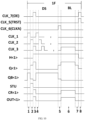
- FIG. 11 is a schematic diagram of a second clock signal and a third clock signal provided by some embodiments of the present disclosure.
- both the second clock signal CLKB and the third clock signal CLKC are pulse signals with a duty ratio of one third
- the third clock signal CLKC and the second clock signal CLKB are separated in timing by a first time interval T1
- the first time interval T1 is equal to two thirds of the period T of the pulse signal.
- the shift register unit 10 provided by some embodiments of the present disclosure further includes a second control circuit 210, which is configured to control the level of the second node QB under the control of the first clock signal CLKA and the level of the fourth node H.
- the second control circuit 210 is connected to the second node QB and the fourth node H, and is configured to receive the first clock signal CLKA and the first voltage VGL1 at a low level. For example, in a blanking period of a frame, when the fourth node H is at a high level and the first clock signal CLKA is at a high level, the second control circuit 210 is turned on, so that the second node QB can be pulled down with the first voltage VGL1 at a low level.
- the transmission circuit 160 in the shift register unit 10 is turned on, so that the first node Q can be charged. While the transmission circuit 160 charges the first node Q, pulling down the level of the second node QB to a low level through the second control circuit 210 can avoid the influence of the second node QB on the first node Q, so that the transmission circuit 160 charges the first node Q more sufficiently, thereby facilitating normally outputting the driving signal OUT by the shift register unit 10 during the blanking period.
- the driving signal OUT may be used to drive sensing transistors in a row of sub-pixel units in the display panel to complete external compensation of the row of sub-pixel units.
- the shift register unit 10 provided by some embodiments of the present disclosure further includes a third control circuit 220.
- the third control circuit 220 is configured to control the level of the second node QB in response to the first input signal STU1.
- the third control circuit 220 is connected to the second node QB, and is configured to receive the first input signal STU1 and the first voltage VGL1 at a low level. For example, in a display period of a frame, the third control circuit 220 is turned on in response to the first input signal STU1, so that the second node QB can be pulled down and reset with the first voltage VGL1 at a low level. Pulling down the second node QB to a low level can avoid the influence of the second node QB on the first node Q, thereby making the first node Q more sufficiently charged in the display period.
- the shift register unit 10 provided by some embodiments of the present disclosure further includes a third reset circuit 230 and a fourth reset circuit 240.
- the third reset circuit 230 is configured to reset the first node Q in response to a display reset signal STD.
- the third reset circuit 230 is connected to the first node Q, and is configured to receive the display reset signal STD and the first voltage VGL1 at a low level.
- the third reset circuit 230 is turned on in response to the display reset signal STD, so that the first node Q can be pulled down and reset with the first voltage VGL1 at a low level.
- a shift register unit 10 of a certain stage may receive the shifting signal CR output by a shift register unit 10 of another stage as the display reset signal STD.
- the fourth reset circuit 240 is configured to reset the first node Q in response to a global reset signal TRST.
- the fourth reset circuit 240 is connected to the first node Q, and is configured to receive the global reset signal TRST and the first voltage VGL1 at a low level.
- the fourth reset circuit 240 in the shift register unit 10 of each stage is turned on in response to the global reset signal TRST, so that the first voltage VGL1 at a low level can pull down and reset the first node Q through the fourth reset circuit 240.
- each node (the first node Q, the second node QB, the third node N, the fourth node H, etc.) and each output terminal (the output terminal OP, the shifting signal output terminal CRT, the driving signal output terminal DST, etc.) are provided to describe the circuit structure better, and do not represent actual components.
- a node represents a meeting point of related circuit connections in a circuit structure, that is, related circuits connected to the node with the same identifier are electrically connected to each other. For example, as shown in FIG.
- the first control circuit 130, the first reset circuit 140, the second control circuit 210, the third control circuit 220, the storage circuit 170, and the second reset circuit 180 are all connected to the second node QB, which means that these circuits are electrically connected to each other.
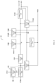
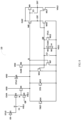
- the shift register unit 10 shown in FIG. 4 may be implemented as the circuit structure shown in FIG. 5 .
- the shift register unit 10 includes a first transistor M1 to a seventeenth transistor M17, a first capacitor C1, and a third capacitor C3.
- the shift register unit 10 of FIGs. 1-3 can be implemented in a similar manner, for example, one electrode of the capacitor as the storage circuit 170 is connected to the second node QB, and the other electrode of the capacitor is connected to other corresponding nodes (e.g., the fourth node H) or is configured to receive a fixed level (e.g., the first voltage VGL1).
- the selection input circuit 151 may be implemented as a first transistor M1.
- a gate electrode of the first transistor M1 is configured to receive the selection control signal OE
- a first electrode of the first transistor M1 is configured to receive the second input signal STU2
- a second electrode of the first transistor M1 is connected to the fourth node H.
- the selection control signal OE is at a high level
- the first transistor M1 is turned on, so that the fourth node H can be charged with the second input signal STU2.
- the second input signal STU2 may be the shifting signal CR output by the shift register unit 10, and the signal timing of the selection control signal OE and the second input signal STU2 are the same, that is, both the selection control signal OE and the second input signal STU2 are at a high level at the same time.
- the transmission control circuit 152 may be implemented as a second transistor M2.
- a gate electrode of the second transistor M2 is connected to the fourth node H, a first electrode of the second transistor M2 is configured to receive the first clock signal CLKA, and a second electrode of the second transistor M2 is connected to the third node N.
- the fourth node H is at a high level
- the second transistor M2 is turned on, so that the first clock signal CLKA can be transmitted to the third node N to pull up the level of the third node N.
- the second reset circuit 180 may be implemented as a third transistor M3.
- a gate electrode of the third transistor M3 is connected to the second node QB, a first electrode of the third transistor M3 is connected to the third node N, and a second electrode of the third transistor M3 is configured to receive the first voltage VGL1 at a low level.
- the third transistor M3 is turned on, and the first voltage VGL1 at a low level may reset the third node N through the third transistor M3.
- the transmission circuit 160 may include a fourth transistor M4.
- a gate electrode of the fourth transistor M4 is connected to the third node N, a first electrode of the fourth transistor M4 is configured to receive the second voltage VDD at a high level, and a second electrode of the fourth transistor M4 is connected to the first node Q.
- the fourth transistor M4 is turned on, and the second voltage VDD may charge the first node Q through the fourth transistor M4.
- the level of the second node QB is a high level
- the first voltage VGL1 at a low level resets the third node N through the third transistor M3 to pull down the level of the third node N. Because the third node N is at a low level, the fourth transistor M4 is turned off, so that the second node VDD can be prevented from charging the first node Q.
- the first input circuit 110 may be implemented as a fifth transistor M5.
- a gate electrode of the fifth transistor is configured to receive the first input signal STU1
- a first electrode of the fifth transistor M5 is configured to receive the second voltage VDD
- a second electrode of the fifth transistor M5 is connected to the first node Q.
- a shift register unit 10 of a certain stage may receive the shifting signal CR of a shift register unit 10 of a previous stage as the first input signal STU1 of the shift register unit 10 of the present stage.
- the fifth transistor M5 is turned on, and the second voltage VDD at a high level can charge the first node Q through the fifth transistor M5 to pull up the level of the first node Q.
- the first electrode of the fifth transistor M5 may also be configured to receive the first input signal STU1, and when being turned on under the control of the first input signal STU1, the fifth transistor M5 may directly charge the first node Q with the first input signal STU1.
- the implementation of the first input circuit 110 is not limited in the embodiments of the present disclosure.
- the output circuit 120 may be implemented to include an eighth transistor M8, a ninth transistor M9, and a third capacitor C3.
- a gate electrode of the eighth transistor M8 is connected to the first node Q, a first electrode of the eighth transistor M8 is configured to receive the third clock signal CLKC, and a second electrode of the eighth transistor M8 is connected to the shifting signal output terminal CRT.
- a gate electrode of the ninth transistor M9 is connected to the first node Q, a first electrode of the ninth transistor M9 is configured to receive the third clock signal CLKC, and a second electrode of the ninth transistor M9 is connected to the driving signal output terminal DST.
- a first electrode of the third capacitor C3 is connected to the first node Q, and a second electrode of the third capacitor C3 is connected to the driving signal output terminal DST.
- the eighth transistor M8 and the ninth transistor M9 are turned on, and the eighth transistor M8 may provide the third clock signal CLKC to the shifting signal output terminal CRT as the shifting signal CR, for example the shifting signal CR may be provided to an adjacent shift register unit 10 as the first input signal STU1 or the display reset signal STD.
- the ninth transistor M9 may provide the third clock signal CLKC to the driving signal output terminal DST as the driving signal OUT.
- the driving signal OUT may drive a row of sub-pixel units in the display panel to perform display scanning; for another example, in a blanking period of a frame, the driving signal OUT may be used to drive sensing transistors in a row of sub-pixel units in the display panel to complete external compensation of the row of sub-pixel units.
- the level of the first node Q can be maintained by the third capacitor C3.
- the second electrode of the third capacitor C3 may also be connected to the shifting signal output terminal CRT, which is not limited in the embodiments of the present disclosure.
- the signal at a high level can further pull up the level of the first node Q through the coupling effect of the third capacitor C3, so that the eighth transistor M8 and the ninth transistor M9 are turned on more sufficiently, thereby facilitating the outputting of the shifting signal CR and the driving signal OUT.
- the first control circuit 130 may be implemented to include a sixth transistor M6 and a seventh transistor M7.
- a gate electrode of the sixth transistor M6 is configured to receive the second clock signal CLKB, a first electrode of the sixth transistor M6 is configured to receive the second voltage VDD, and a second electrode of the sixth transistor M6 is connected to the second node QB.
- a gate electrode of the seventh transistor M7 is connected to the first node Q, a first electrode of the seventh transistor M7 is connected to the second node QB, and a second electrode of the seventh transistor M7 is configured to receive the first voltage VGL1.
- the seventh transistor M7 when the level of the first node Q is a high level, the seventh transistor M7 is turned on, and the first voltage VGL1 at a low level may reset the second node QB.
- the sixth transistor M6 when the level of the first node Q is a low level and the level of the second clock signal CLKB is a high level, the sixth transistor M6 is turned on, the seventh transistor M7 is turned off, and the second voltage VDD at a high level can charge the second node QB through the sixth transistor M6, thereby pulling up the level of the second node QB to a high level.
- the second control circuit 210 may be implemented to include a tenth transistor M10 and an eleventh transistor M11.
- a gate electrode of the tenth transistor M10 is configured to receive the first clock signal CLKA, a first electrode of the tenth transistor M10 is connected to the second node QB, a second electrode of the tenth transistor M10 is connected to a first electrode of the eleventh transistor M11, a gate electrode of the eleventh transistor M11 is connected to the fourth node H, and a second electrode of the eleventh transistor M11 is configured to receive the first voltage VGL1.
- the first clock signal CLKA is at a high level and the fourth node H is at a high level
- the tenth transistor M10 and the eleventh transistor M11 are turned on, so that the first voltage VGL1 at a low level can pull down and reset the second node QB.
- the third control circuit 220 may be implemented as a twelfth transistor M12.
- a gate electrode of the twelfth transistor M12 is configured to receive the first input signal STU1
- a first electrode of the twelfth transistor M12 is connected to the second node QB
- a second electrode of the twelfth transistor M12 is configured to receive the first voltage VGL1.
- the twelfth transistor M12 is turned on, so that the first voltage VGL1 at a low level can pull down and reset the second node QB.
- the first reset circuit 140 may be implemented to include a fifteenth transistor M15, a sixteenth transistor M16, and a seventeenth transistor M17.
- Agate electrode of the fifteenth transistor M15 is connected to the second node QB, a first electrode of the fifteenth transistor M15 is connected to the first node Q, and a second electrode of the fifteenth transistor M15 is configured to receive the first voltage VGL1.
- a gate electrode of the sixteenth transistor M16 is connected to the second node QB, a first electrode of the sixteenth transistor M16 is connected to the shifting signal output terminal CRT, and a second electrode of the sixteenth transistor M16 is configured to receive the first voltage VGL1.
- a gate electrode of the seventeenth transistor M17 is connected to the second node QB, a first electrode of the seventeenth transistor M17 is connected to the driving signal output terminal DST, and a second electrode of the seventeenth transistor M17 is configured to receive the third voltage VGL2.
- the fifteenth transistor M15 and the sixteenth transistor M16 are turned on, so that the first voltage VGL1 at a low level can reset the first node Q and the shifting signal output terminal CRT; meanwhile, the seventeenth transistor M17 is turned on, so that the third voltage VGL2 at a low level can reset the driving signal output terminal DST.
- the second electrode of the seventeenth transistor M17 may also be configured to receive the first voltage VGL 1, so as to reset the driving signal output terminal DST with the first voltage VGL1.
- the third reset circuit 230 may be implemented as a thirteenth transistor M13.
- a gate electrode of the thirteenth transistor M13 is configured to receive the display reset signal STD, a first electrode of the thirteenth transistor M13 is connected to the first node Q, and a second electrode of the thirteenth transistor M13 is configured to receive the first voltage VGL1.
- a shift register unit 10 of a certain stage can receive the shifting signal CR of a shift register unit 10 of a next stage as the display reset signal STD of the shift register unit 10 of the present stage.
- the display reset signal STD is at a high level
- the thirteenth transistor M13 is turned on, so that the first voltage VGL1 at a low level can pull down and reset the first node Q.
- the fourth reset circuit 240 may be implemented as a fourteenth transistor M14.
- a gate electrode of the fourteenth transistor M14 is configured to receive the global reset signal TRST, a first electrode of the fourteenth transistor M14 is connected to the first node Q, and a second electrode of the fourteenth transistor M14 is configured to receive the first voltage VGL1.
- the fourteenth transistor M14 in the shift register unit 10 of each stage is turned on in response to the global reset signal TRST, thereby implementing global resetting of the gate driving circuit.
- the storage circuit 170 may be implemented as a first capacitor C1, a first electrode of the first capacitor C1 is connected to the fourth node H, and a second electrode of the first capacitor C1 is connected to the second node QB.
- the first capacitor C1 can stabilize the level of the second node QB. For example, when the second clock signal CLKB is at a high level, the second voltage VDD charges the second node QB through the sixth transistor M6, thereby pulling up the level of the second node QB to a high level. Then, when the level of the second clock signal CLKB becomes a low level, the sixth transistor M6 is turned off, that is, the charging path for the second node QB is cut off.
- the first capacitor C1 because the first capacitor C1 is connected to the second node QB, the first capacitor C1 can maintain the high level of the second node QB, thereby preventing the influence caused by the drifting of the level of the second node QB on the level of the first node Q.
- the first capacitor C1 is connected to the fourth node H in addition to the second node QB, so that the first capacitor C1 can also be used to stabilize the level of the fourth node H. In this way, the first capacitor C1 can be reused to reduce the number of capacitors, thereby simplifying the circuit structure and reducing the bezel size of the display device using the shift register unit 10, which is more conducive to improving the PPI of the display device.
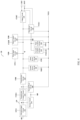
- the shift register unit 10 may also be implemented as the circuit structure shown in FIG. 6 . Only the differences between the shift register unit 10 shown in FIG. 6 and the shift register unit 10 shown in FIG. 5 will be described below, and the same portions will not be described again.
- the shift register unit 10 does not include the second reset circuit 180, that is, does not include the third transistor M3.
- the gate electrode of the fourth transistor M4 is configured to receive the first clock signal CLKA, the first electrode of the fourth transistor M4 is connected to the third node N, and the second electrode of the fourth transistor M4 is connected to the first node Q.
- the level of the fourth node H is a high level and the level of the first clock signal CLKA is a high level
- both the second transistor M2 and the fourth transistor M4 are turned on, so that the first clock signal CLKA at a high level can charge the first node Q through the second transistor M2 and the fourth transistor M4.
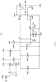
- the shift register unit 10 may also be implemented as the circuit structure shown in FIG. 7 . Only the differences between the shift register unit 10 shown in FIG. 7 and the shift register unit 10 shown in FIG. 5 will be described below, and the same portions will not be described again.
- the selection input circuit 151 is implemented to include a first transistor M1 and a first capacitor C1, and the storage circuit 170 is implemented as a second capacitor C2.
- the first electrode of the first capacitor C1 is connected to the fourth node H, and the second electrode of the first capacitor C1 is connected to the third node N.
- a first electrode of the second capacitor C2 is connected to the second node QB, and a second electrode of the second capacitor C2 is configured to receive a fixed level, for example, to receive the first voltage VGL1.
- the connection manner of the second capacitor C2 is not limited in the embodiment of the present disclosure, and the second electrode of the second capacitor C2 may also receive other fixed levels, such as the second voltage VDD, the third voltage VGL2, and so on.
- the second capacitor C2 may be used to stabilize the level of the second node QB.
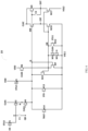
- the shift register unit 10 may also be implemented as the circuit structure shown in FIG. 8 . Only the differences between the shift register unit 10 shown in FIG. 8 and the shift register unit 10 shown in FIG. 7 will be described below, and the same portions will not be described again.
- the first electrode of the first capacitor C1 is connected to the fourth node H, and the second electrode of the first capacitor C1 is configured to receive the first voltage VGL1.
- the connection manner of the first capacitor C1 is not limited in the embodiment of the present disclosure.
- the second electrode of the first capacitor C1 may also be configured to receive other fixed levels, for example, to receive the second voltage VDD, the third voltage VGL2, and so on.
- transistors in the shift register unit 10 are all described as N-type transistors as an example.
- the transistors adopted in the embodiments of the present disclosure may all be thin film transistors, field effect transistors, or other switching elements with the same characteristics.
- the thin film transistors are taken as an example for description.
- the source electrode and the drain electrode of a transistor adopted here may be symmetrical in structure, so the source electrode and the drain electrode of the transistor may have no difference in structure.
- one electrode is directly described as the first electrode and the other electrode is directly described as the second electrode.
- transistors can be divided into N-type and P-type transistors according to their characteristics.
- the turn-on voltage is a high-level voltage (e.g., 5V, 10V or other suitable voltage)
- the turn-off voltage is a low-level voltage (e.g., 0V, -5V, -10V or other suitable voltage)
- the transistors in the following embodiments are also described as N-type transistors as an example, which will not be repeated.
- the embodiments of the present disclosure include but are not limited thereto, for example, one or more transistors in the shift register unit provided by the embodiments of the present disclosure may also adopt P-type transistors.
- the turn-on voltage is a low-level voltage (e.g., 0V, - 5V, -10V or other suitable voltage)
- the turn-off voltage is a high-level voltage (e.g., 5V, 10V or other suitable voltage).
- the first capacitor C1 may be used to stabilize the level of the fourth node H or the second node QB
- the second capacitor C2 may be used to stabilize the level of the second node QB
- the third capacitor C3 may be used to stabilize the level of the first node Q.
- the first capacitor C1, the second capacitor C2, and the third capacitor C3 may be capacitor devices prepared by a manufacturing process, for example, the capacitor device is implemented by preparing a special capacitor electrode, and each electrode of the capacitor can be implemented by a metal layer, a semiconductor layer (e.g., doped polysilicon), etc., or in some examples, by setting circuit wiring parameters, the first capacitor C1, the second capacitor C2, and the third capacitor C3 may also be implemented by parasitic capacitances between various devices.
- the connection manner of the first capacitor C1, the second capacitor C2 and the third capacitor C3 is not limited to the manner described above, and may be other suitable connection manners as long as the levels written to the fourth node H, the second node QB, and the first node Q can be stored.
- the gate driving circuit 20 includes a plurality of cascaded shift register units 10, where any one or more of the shift register units 10 may adopt the structure of the shift register unit 10 provided by the embodiments of the present disclosure or a modification thereof.
- A1, A2, A3, and A4 in FIG. 9 represent four cascaded shift register units 10.
- output signals of A1, A2, A3, and A4 can respectively drive four rows of sub-pixel units in the display panel.
- A1, A2, A3, and A4 can drive the first, second, third, and fourth rows of sub-pixel units of the display panel, respectively.
- the gate driving circuit 20 provided by the embodiment of the present disclosure can stabilize the level of the second node QB, and when there is no need to output a driving signal, the second node QB can be stably maintained at a high level, so that the level of the first node Q does not drift and is stably maintained at a low level, thereby avoiding the problem that the gate driving circuit 20 outputs signals multiple times.
- the gate driving circuit 20 can also realize random compensation, so as to avoid the problems of poor display effects such as scanning lines and uneven display brightness caused by the progressive sequential compensation.
- the gate driving circuit 20 includes a first sub-clock signal line CLK_1, a second sub-clock signal line CLK_2, and a third sub-clock signal line CLK_3.
- the (3n-2)-th shift register unit (e.g., the first shift register unit A1) is connected to the first sub-clock signal line CLK_1 to receive the second clock signal CLKB for the (3n-2)-th shift register unit, and the (3n-2)-th shift register unit is connected to the third sub-clock signal line CLK_3 to receive the third clock signal CLKC for the (3n-2)-th shift register unit.
- the (3n-1)-th shift register unit (e.g., the second shift register unit A2) is connected to the second sub-clock signal line CLK_2 to receive the second clock signal CLKB for the (3n-1)-th shift register unit, and the (3n-1)-th shift register unit is connected to the first sub-clock signal line CLK_1 to receive the third clock signal CLKC for the (3n-1)-th shift register unit.
- the (3n)-th shift register unit (e.g., the third shift register unit A3) is connected to the third sub-clock signal line CLK_3 to receive the second clock signal CLKB for the (3n)-th shift register unit, and the (3n)-th shift register unit is connected to the second sub-clock signal line CLK_2 to receive the third clock signal CLKC for the (3n)-th shift register unit; n is an integer greater than zero.
- the signal timing provided by the first sub-clock signal line CLK_1, the second sub-clock signal line CLK_2, and the third sub-clock signal line CLK_3 is shown in FIG. 10 .
- the signals provided by the first sub-clock signal line CLK_1, the second sub-clock signal line CLK 2, and the third sub-clock signal line CLK_3 are all pulse signals with a duty ratio of one third.
- the second clock signal CLKB and the third clock signal CLKC are provided to the shift register unit 10 of each stage through three sub-clock signal lines, so as to reduce the number of signal lines, thereby simplifying the circuit structure and reducing the bezel size of the display device using the shift register unit 10, which is more conducive to improving the PPI of the display device.
- the gate driving circuit 20 further includes a fourth sub-clock signal line CLK_4, a fifth sub-clock signal line CLK_5, a sixth sub-clock signal line CLK_6, and a seventh sub-clock signal line CLK_7.
- the shift register unit 10 of each stage in the gate driving circuit 20 is connected to the fourth sub-clock signal line CLK_4 to receive the second voltage VDD.
- Each shift register unit 10 in the gate driving circuit 20 is connected to the fifth sub-clock signal line CLK_5 to receive the global reset signal TRST.
- the shift register unit 10 of each stage in the gate driving circuit 20 is connected to the sixth sub-clock signal line CLK_6 to receive the first clock signal CLKA.
- the shift register unit 10 of each stage in the gate driving circuit 20 is connected to the seventh sub-clock signal line CLK_7 to receive the selection control signal OE.
- shift register units 10 of other stages are each connected to the shift register unit 10 of a previous stage to receive the shifting signal CR as the first input signal STU1.
- shift register units 10 of other stages are each connected to the shift register unit 10 of a next stage to receive the shifting signal CR as the display reset signal STD.
- cascading relationship shown in FIG. 9 is only an example, and according to the description of the present disclosure, other cascading relationships may also be adopted according to actual conditions.
- the shift register unit 10 in the gate driving circuit 20 shown in FIG. 9 may adopt the circuit structure shown in FIG. 5 .
- FIG. 10 shows a signal timing diagram of the gate driving circuit 20 in FIG. 9 in a working state.
- H ⁇ 1> represents the fourth node H in the shift register unit 10 of the first stage, and the shift register unit 10 of the first stage corresponds to the first row of sub-pixel units in the display panel.
- Q ⁇ 1> represents the first node Q in the shift register unit 10 of the first stage.
- QB ⁇ 1> represents the second node QB in the shift register unit 10 of the first stage.
- the numbers in parentheses indicate the row number of sub-pixel units in the display panel corresponding to the shift register unit 10. The same case applies to following embodiments, and will not be repeated.
- STU represents the first input signal provided to the shift register unit 10 of the first stage
- CR ⁇ 1> represents the shifting signal CR output by the shift register unit 10 of the first stage
- OUT ⁇ 1> represents the driving signal OUT output by the shift register unit 10 of the first stage.
- CR ⁇ 1> is the same as OUT ⁇ 1>.
- 1F represents a first frame
- DS represents a display period in the first frame
- BL represents a blanking period in the first frame. It should be noted that the signal level in the signal timing diagram shown in FIG. 10 is only schematic and does not represent the true level value.
- the first sub-clock signal line CLK_1 provides a high level. Because the shift register unit 10 of the first stage is connected to the first sub-clock signal line CLK_1 to receive the second clock signal CLKB, the second clock signal CLKB received by the shift register unit 10 of the first stage in the first stage 1 is at a high level. As shown in FIG. 5 , the sixth transistor M6 is turned on under the control of the second clock signal CLKB at a high level, and the second voltage VDD at a high level charges the second node QB ⁇ 1> through the sixth transistor M6, thereby pulling up the second node QB ⁇ 1> to a high level.
- the fifteenth transistor M15, the sixteenth transistor M16, and the seventeenth transistor M17 are turned on, so that the first node Q ⁇ 1>, the shifting signal output terminal CRT, and the driving signal output terminal DST can be reset.
- the first input signal STU received by the shift register unit 10 of the first stage is at a high level and the fifth transistor M5 is turned on, so that the second voltage VDD at a high level can charge the first node Q ⁇ 1> through the fifth transistor M5, thereby pulling up the first node Q ⁇ 1> to a high level.
- the eighth transistor M8 and the ninth transistor M9 are turned on under the control of the level of the first node Q ⁇ 1>, but because the third clock signal CLKC provided by the third sub-clock signal line CLK_3 in this case is at a low level, the shifting signal CR ⁇ 1> and the driving signal OUT ⁇ 1> output by the shift register unit 10 of the first stage are at a low level.
- the pre-charging operation is completed for the first node in the shift register unit 10 of the first stage.
- the seventh transistor M7 is turned on.
- the twelfth transistor M12 is turned on.
- the first voltage VGL1 at a low level can reset the second node QB ⁇ 1> through the seventh transistor M7 and the twelfth transistor M12, so that the level of the second node QB ⁇ 1> is pulled down to the low level. Pulling down the level of the second node QB ⁇ 1> to a low level can prevent the level of the second node QB ⁇ 1> from affecting the pre-charge operation of the first node Q ⁇ 1>.
- the level of the third clock signal CLKC provided by the third sub-clock signal line CLK_3 becomes a high level, so the levels of the shifting signal CR ⁇ 1> and the driving signal OUT ⁇ 1> output by the shift register unit 10 of the first stage become high levels.
- the shifting signal CR ⁇ 1> output by the shift register unit 10 of the first stage may be provided to the second shift register unit 10 as the first input signal STU1, and the driving signal OUT ⁇ 1> output by the shift register unit 10 of the first stage can be provided to the first row of sub-pixel units in the display panel to drive the first row of sub-pixel units to perform a display operation.
- the driving signal OUT ⁇ 1> output by the shift register unit 10 of the first stage at a high level can couple and pull up the level of the first node Q ⁇ 1>, thereby further pulling up the level of the first node Q ⁇ 1>.
- the level of the first node Q ⁇ 1> is higher in the third stage 3, so that the seventh transistor M7 is turned on more sufficiently, thereby pulling down the level of the second node QB ⁇ 1> to a lower level.
- a fourth stage 4 because the second shift register unit 10 is connected to the first sub-clock signal line CLK_1 to receive the third clock signal CLKC, the second shift register unit 10 outputs the shifting signal CR at a high level in the fourth stage 4, and the shifting signal CR is provided to the shift register unit 10 of the first stage as the display reset signal STD. Because the display reset signal STD is at a high level, the thirteenth transistor M13 is turned on and thus the first voltage VGL1 at a low level pulls down and resets the first node Q ⁇ 1> through the thirteenth transistor M13, thereby pulling down the level of the first node Q ⁇ 1> to a low level.
- the seventh transistor M7 is turned off. In this case, because the second clock signal CLKB received by the shift register unit 10 of the first stage in the fourth stage 4 is at a high level, the sixth transistor M6 is turned on, and the second voltage VDD at a high level can charge the second node QB ⁇ 1>, thereby pulling up the level of the second node QB ⁇ 1> to a high level.
- the seventh transistor M7, the sixteenth transistor M16 and the seventeenth transistor M17 are turned on under the control of the level of the second node QB ⁇ 1>, and the first node Q ⁇ 1>, the shifting signal output terminal CRT, and the driving signal output terminal DST can be reset, so that the levels of the shifting signal CR ⁇ 1> and the driving signal OUT ⁇ 1> output by the shift register unit 10 of the first stage become low levels.
- the first capacitor C1 can maintain the high level of the second node QB ⁇ 1>, even if the second clock signal CLKB received by the shift register unit 10 of the first stage becomes a low level, the level of the second node QB ⁇ 1> will not be affected, so that the level of the second node QB ⁇ 1> can be prevented from drifting, and the level of the first node Q ⁇ 1> can be prevented from being pulled up to a high level when the shift register unit 10 does not need to output a driving signal, thereby avoiding the problem that the shift register unit 10 outputs signals multiple times.
- the shift register unit 10 of the first stage drives the first row of sub-pixel units in the display panel to complete the display operation, and so on, and the shift register units 10 of the second stage, the third stage and other stages drive the sub-pixel units in the display panel row by row to complete the display drive for one frame. Then, the display period of the first frame ends.
- the fourth node H ⁇ 1> is also charged in the display period DS of the first frame 1F.
- the following operations are also performed in the display period DS of the first frame 1F.
- the selection control signal OE provided by the seventh sub-clock signal line CLK_7 is at a high level, so the first transistor M1 is turned on.
- the second input signal STU2 received by the shift register unit 10 of the first stage can be the same as the shifting signal CR ⁇ 1> output by the shift register unit of the first stage, so that the second input signal STU2 at a high level can charge the fourth node H ⁇ 1>, thereby pulling up the level of the fourth node H ⁇ 1> to a high level.
- the above charging process for the fourth node H ⁇ 1> is only an example, and the embodiments of the present disclosure include but are not limited thereto.
- the second input signal STU2 received by the shift register unit 10 of the first stage may also be the same as the shifting signal CR output by the shift register units 10 of other stages, as long as the signal timing of the signal provided to the seventh sub-clock signal line CLK_7 is the same as the signal timing of the second input signal STU2.
- the high level of the fourth node H ⁇ 1> can be maintained until the blanking period BL of the first frame 1F.
- the following operations are performed in the blanking period BL of the first frame 1F.
- the first clock signal CLKA provided by the sixth sub-clock signal line CLK_6 is at a high level. Because the fourth node H ⁇ 1> remains at a high level in this stage, the second transistor M2 is turned on, and the first clock signal CLKA at a high level is transmitted to the third node N through the second transistor M2, so that the third node N becomes a high level.
- the fourth transistor M4 is turned on under the control of the third node N, so that the second voltage VDD at a high level can charge the first node Q ⁇ 1>, thereby pulling up the level of the first node Q ⁇ 1> to a high level.
- the tenth transistor M10 and the eleventh transistor M11 are turned on, so that the first voltage VGL1 at a low level can reset the second node QB ⁇ 1>, thereby pulling down the level of the second node QB ⁇ 1> to a low level.
- the level of the third clock signal CLKC provided by the third sub-clock signal line CLK_3 becomes a high level, so the levels of the shifting signal CR ⁇ 1> and the driving signal OUT ⁇ 1> output by the first stage shift register unit 10 become a high level.
- the driving signal OUT ⁇ 1> can be used to drive sensing transistors in the first row of sub-pixel units in the display panel to achieve external compensation.
- the first node Q ⁇ 1> is still maintained at a high level, so that the eighth transistor M8 and the ninth transistor M9 remain to be turned on.
- the level of the third clock signal CLKC provided by the third sub-clock signal line CLK_3 becomes a low level, the levels of the shifting signal CR ⁇ 1> and the driving signal OUT ⁇ 1> output by the shift register unit 10 of the first stage become a low level.
- the level of the first node Q ⁇ 1> will also decrease.
- the fifth sub-clock signal line CLK_5 and the seventh sub-clock signal line CLK_7 provide high levels, and the fourteenth transistor M14 in the shift register unit 10 of each stage in the gate driving circuit 20 is turned on, so that the first node Q in the shift register unit 10 of each stage can be reset; the first transistor M1 in the shift register unit 10 of each stage in the gate driving circuit 20 is turned on, and because the second input signal STU2 received at this time is at a low level, the fourth node H in the shift register unit 10 of each stage can be reset, thereby completing the global reset.
- the driving signal corresponding to the n-th row of sub-pixel units of the display panel needs to be output during the blanking period of a frame
- the corresponding fourth node H needs to be pulled up to a high level during the display period DS of the frame, and during the blanking period BL of the frame, the first clock signal CLKA at a high level is provided to pull up the level of the first node Q, and then in the case where the driving signal at a high level needs to be output, the third clock signal CLKC at a high level is provided, n is an integer greater than zero.
- the timing of the two signals being the same refers to time synchronization of being at a high level, and does not require that the two signals have the same amplitude.
- the display device 1 includes a gate driving circuit 20 provided by the embodiments of the present disclosure and a plurality of sub-pixel units 510 arranged in an array.
- the display device 1 further includes a display panel 50, and a pixel array formed by a plurality of sub-pixel units 510 is provided in the display panel 50.
- a driving signal OUT output from each shift register unit 10 in the gate driving circuit 20 is provided to different rows of sub-pixel units 510.
- the gate driving circuit 20 is electrically connected to the sub-pixel unit 510 through a gate line GL.
- the gate driving circuit 20 is used to provide the driving signal OUT to the pixel array.
- the driving signal OUT can be used to drive the scanning transistor and the sensing transistor in the sub-pixel unit 510.
- the display device 1 may further include a data driving circuit 30 for providing data signals to the pixel array.
- the data driving circuit 30 is electrically connected to the sub-pixel unit 510 through a data line DL.
- the display device 1 in the present embodiment may be any product or component with a display function such as a liquid crystal panel, an liquid crystal television, a display, an OLED panel, an OLED television, an electronic paper display device, a mobile phone, a tablet computer, a notebook computer, a digital photo frame, a navigator, and the like.
- a display function such as a liquid crystal panel, an liquid crystal television, a display, an OLED panel, an OLED television, an electronic paper display device, a mobile phone, a tablet computer, a notebook computer, a digital photo frame, a navigator, and the like.
- An embodiment of the present disclosure also provides a driving method, which can be used to drive the shift register unit 10 provided by the embodiments of the present disclosure, a plurality of the shift register units 10 can be cascaded to form the gate driving circuit provided by an embodiment of the present disclosure, and the gate driving circuit is used to drive the display panel to display at least one frame of pictures.
- the driving method includes: controlling, by the first input circuit 110, the level of the first node Q in response to the first input signal STU1; providing, by the output circuit 120, the output signal at the output terminal OP under the control of the level of the first node Q; controlling, by the first control circuit 130, the level of the second node QB under the control of the level of the first node Q; resetting, by the first reset circuit 140, the first node Q and the output terminal OP which includes, for example, the shifting signal output terminal CRT and the driving signal output terminal DST, under the control of the level of the second node QB,; controlling, by the second input circuit 150, the level of the third node N in response to the selection control signal OE; controlling, by the transmission circuit 160, the level of the first node Q according to the level of the third node N; and stabilizing, by the storage circuit 170, the level of the second node QB.
Landscapes
- Engineering & Computer Science (AREA)
- Physics & Mathematics (AREA)
- Computer Hardware Design (AREA)
- General Physics & Mathematics (AREA)
- Theoretical Computer Science (AREA)
- Control Of Indicators Other Than Cathode Ray Tubes (AREA)
- Liquid Crystal Display Device Control (AREA)
Claims (12)
- Schieberegistereinheit (10), umfassend eine erste Eingangsschaltung (110), eine Ausgangsschaltung (120), eine erste Steuerschaltung (130), eine erste Rücksetzschaltung (140), eine zweite Eingangsschaltung (150), eine Übertragungsschaltung (160) und eine Speicherschaltung (170);wobei die erste Eingangsschaltung (110) konfiguriert ist, um einen Pegel eines ersten Knotens (Q) in Antwort auf ein erstes Eingangssignal (STU1) zu steuern,die Ausgangsschaltung (120) konfiguriert ist, um ein Ausgangssignal an einem Ausgangsanschluss (OP) unter Steuerung des Pegels des ersten Knotens (Q) bereitzustellen,die erste Steuerschaltung (130) konfiguriert ist, um einen Pegel eines zweiten Knotens (QB) unter Steuerung des Pegels des ersten Knotens (Q) zu steuern,die erste Rücksetzschaltung (140) konfiguriert ist, um den ersten Knoten (Q) und den Ausgangsanschluss (OP) unter Steuerung des Pegels des zweiten Knotens (QB) zurückzusetzen,die zweite Eingangsschaltung (150) konfiguriert ist, um einen Pegel eines dritten Knotens (N) in Antwort auf ein Auswahlsteuersignal (OE) zu steuern, wobei die zweite Eingangsschaltung (150) eine Auswahleingangsschaltung (151) und eine Übertragungssteuerschaltung (152) umfasst, wobei die Auswahleingangsschaltung (151) konfiguriert ist, um ein zweites Eingangssignal (STU2) an einen vierten Knoten (H) unter Steuerung des Pegels des Auswahlsteuersignals (OE) zu übertragen; unddie Übertragungssteuerschaltung (152) an den dritten Knoten (N) und den vierten Knoten (H) angeschlossen ist und konfiguriert ist, um ein erstes Taktsignal (CLKA) an den dritten Knoten (N) unter Steuerung des Pegels des vierten Knotens (H) zu übertragen,die Übertragungsschaltung (160) konfiguriert ist, um den Pegel des ersten Knotens (Q) gemäß dem Pegel des dritten Knotens (N) zu steuern, unddie Speicherschaltung (170) elektrisch an den zweiten Knoten (QB) angeschlossen ist und konfiguriert ist, um den Pegel des zweiten Knotens (QB) zu stabilisieren, die Speicherschaltung (170) einen ersten Kondensator (C1) umfasst, eine erste Elektrode des ersten Kondensators (C1) an den vierten Knoten (H) angeschlossen ist und eine zweite Elektrode des ersten Kondensators (C1) an den zweiten Knoten (QB) angeschlossen ist,wobei die erste Eingangsschaltung (110) einen fünften Transistor (M5) umfasst, die erste Steuerschaltung (130) einen sechsten Transistor (M6) und einen siebten Transistor (M7) umfasst, die Ausgangsschaltung (120) einen achten Transistor (M8), einen neunten Transistor (M9) und einen dritten Kondensator (C3) umfasst, der Ausgangsanschluss (OP) einen Schiebesignal-Ausgangsanschluss (CRT) und einen Treibersignal-Ausgangsanschluss (DST) umfasst, und der Schiebesignal-Ausgangsanschluss (CRT) und der Treibersignal-Ausgangsanschluss (DST) konfiguriert sind, um das Ausgangssignal auszugeben;eine Gate-Elektrode des fünften Transistors (M5) konfiguriert ist, um das erste Eingangssignal (STU1) zu empfangen, eine erste Elektrode des fünften Transistors (M5) konfiguriert ist, um das erste Eingangssignal (STU1) oder die zweite Spannung (VDD) zu empfangen, und eine zweite Elektrode des fünften Transistors (M5)an den ersten Knoten (Q) angeschlossen ist;eine Gate-Elektrode des sechsten Transistors (M6) konfiguriert ist, um ein zweites Taktsignal (CLKB) zu empfangen, eine erste Elektrode des sechsten Transistors (M6) konfiguriert ist, um die zweite Spannung (VDD) zu empfangen, und eine zweite Elektrode des sechsten Transistors (M6) an den zweiten Knoten (QB) angeschlossen ist;eine Gate-Elektrode des siebten Transistors (M7) an den ersten Knoten (Q) angeschlossen ist, eine erste Elektrode des siebten Transistors (M7) an den zweiten Knoten (QB) angeschlossen ist, und eine zweite Elektrode des siebten Transistors (M7) konfiguriert ist, um eine erste Spannung (VGL1) zu empfangen;eine Gate-Elektrode des achten Transistors (M8) an den ersten Knoten (Q) angeschlossen ist, eine erste Elektrode des achten Transistors (M8) konfiguriert ist, um ein drittes Taktsignal (CLKC) zu empfangen, und eine zweite Elektrode des achten Transistors (M8) an den Schiebesignal-Ausgangsanschluss (CRT) angeschlossen ist;eine Gate-Elektrode des neunten Transistors (M9) an den ersten Knoten (Q) angeschlossen ist, eine erste Elektrode des neunten Transistors (M9) konfiguriert ist, um das dritte Taktsignal (CLKC) zu empfangen, und eine zweite Elektrode des neunten Transistors (M9) an den Treibersignal-Ausgangsanschluss (DST) angeschlossen ist; undeine erste Elektrode des dritten Kondensators (C3) an den ersten Knoten (Q) angeschlossen ist, und eine zweite Elektrode des dritten Kondensators (C3) an den Treibersignal-Ausgangsanschluss (DST) angeschlossen ist.
- Schieberegistereinheit (10) gemäß Anspruch 1, außerdem umfassend eine zweite Rücksetzschaltung (180), wobei die zweite Rücksetzschaltung (180) konfiguriert ist, um den dritten Knoten (N) unter Steuerung des Pegels des zweiten Knotens (QB) zurückzusetzen.
- Schieberegistereinheit (10) gemäß Anspruch 2, wobei die zweite Rücksetzschaltung (180) an den zweiten Knoten (QB) und den dritten Knoten (N) angeschlossen ist.
- Schieberegistereinheit (10) gemäß einem der Ansprüche 1 bis 3, wobei die Auswahleingangsschaltung (151) einen ersten Transistor (M1) umfasst und die Übertragungssteuerschaltung (152) einen zweiten Transistor (M2) umfasst und die Übertragungsschaltung (160) einen vierten Transistor (M4) umfasst;eine Gate-Elektrode des ersten Transistors (M1) konfiguriert ist, um das Auswahlsteuersignal (OE) zu empfangen, eine erste Elektrode des ersten Transistors (M1) konfiguriert ist, um das zweite Eingangssignal (STU2) zu empfangen, und eine zweite Elektrode des ersten Transistors (M1) an den vierten Knoten (H) angeschlossen ist;eine Gate-Elektrode des zweiten Transistors (M2) an den vierten Knoten (H) angeschlossen ist, eine erste Elektrode des zweiten Transistors (M2)konfiguriert ist, um das erste Taktsignal (CLKA) zu empfangen, und eine zweite Elektrode des zweiten Transistors (M2) an den dritten Knoten (N) angeschlossen ist; undeine Gate-Elektrode des vierten Transistors (M4) konfiguriert ist, um das erste Taktsignal (CLKA) zu empfangen, eine erste Elektrode des vierten Transistors (M4) an den dritten Knoten (N) angeschlossen ist, und eine zweite Elektrode des vierten Transistors (M4) an den ersten Knoten (Q) angeschlossen ist.
- Schieberegistereinheit (10) gemäß Anspruch 2, wobei die Auswahleingangsschaltung (151) einen ersten Transistor (M1) umfasst, die Übertragungssteuerschaltung (152) einen zweiten Transistor (M2) umfasst, die zweite Rücksetzschaltung (180) einen dritten Transistor (M3) umfasst und die Übertragungsschaltung (160) einen vierten Transistor (M4) umfasst;eine Gate-Elektrode des ersten Transistors (M1) konfiguriert ist, um das Auswahlsteuersignal (OE) zu empfangen, eine erste Elektrode des ersten Transistors (M1) konfiguriert ist, um das zweite Eingangssignal (STU2) zu empfangen, und eine zweite Elektrode des ersten Transistors (M1) mit dem vierten Knoten (H) verbunden ist;eine Gate-Elektrode des zweiten Transistors (M2) an den vierten Knoten (H) angeschlossen ist, eine erste Elektrode des zweiten Transistors (M2) konfiguriert ist, um das erste Taktsignal (CLKA) zu empfangen, und eine zweite Elektrode des zweiten Transistors (M2) an den dritten Knoten (N) angeschlossen ist;eine Gate-Elektrode des dritten Transistors (M3) an den zweiten Knoten (QB) angeschlossen ist, eine erste Elektrode des dritten Transistors (M3) an den dritten Knoten (N) angeschlossen ist, und eine zweite Elektrode des dritten Transistors (M3) konfiguriert ist, um eine erste Spannung (VGL1) zu empfangen; undeine Gate-Elektrode des vierten Transistors (M4) an den dritten Knoten (N) angeschlossen ist, eine erste Elektrode des vierten Transistors (M4) konfiguriert ist, um das erste Taktsignal (CLKA) oder eine zweite Spannung (VDD) zu empfangen, und eine zweite Elektrode des vierten Transistors (M4) an den ersten Knoten (Q) angeschlossen ist.
- Schieberegistereinheit (10) gemäß einem der Ansprüche 1 bis 5, wobei
sowohl das zweite Taktsignal (CLKB) als auch das dritte Taktsignal (CLKC) Impulssignale mit einem Tastverhältnis von einem Drittel sind, das dritte Taktsignal (CLKC) und das zweite Taktsignal (CLKB) zeitlich mittels eines erstes Zeitintervalls (T1) getrennt sind, und das erste Zeitintervall (T1) gleich zwei Dritteln einer Periode des Impulssignals ist. - Schieberegistereinheit (10) gemäß einem der Ansprüche 1 bis 6,außerdem umfassend eine zweite Steuerschaltung (210), wobei die zweite Steuerschaltung (210) konfiguriert ist, um den Pegel des zweiten Knotens (QB) unter Steuerung des ersten Taktsignals (CLKA) und den Pegel des vierten Knotens (H) zu steuern;die zweite Steuerschaltung (210) einen zehnten Transistor (M10) und einen elften Transistor (M11) umfasst,eine Gate-Elektrode des zehnten Transistors (M10) konfiguriert ist, um das erste Taktsignal (CLKA) zu empfangen, eine erste Elektrode des zehnten Transistors (M10) an den zweiten Knoten (QB) angeschlossen ist, und eine zweite Elektrode des zehnten Transistors (M10) an eine erste Elektrode des elften Transistors (M11) angeschlossen ist,eine Gate-Elektrode des elften Transistors (M11) an den vierten Knoten (H) angeschlossen ist, und eine zweite Elektrode des elften Transistors (M11) konfiguriert ist, um die erste Spannung (VGL1) zu empfangen.
- Schieberegistereinheit (10) gemäß einem der Ansprüche 1 bis 7, außerdem umfassend eine dritte Steuerschaltung (220), wobei die dritte Steuerschaltung (220) konfiguriert ist, um den Pegel des zweiten Knotens (QB) in Reaktion auf das erste Eingangssignal (STU1) zu steuern;optional die dritte Steuerschaltung (220) einen zwölften Transistor (M12) umfasst,eine Gate-Elektrode des zwölften Transistors (M12) konfiguriert ist, um das erste Eingangssignal (STU1) zu empfangen, eine erste Elektrode des zwölften Transistors (M12) an den zweiten Knoten (QB) angeschlossen ist, und eine zweite Elektrode des zwölften Transistors (M12) konfiguriert ist, um die erste Spannung (VGL1) zu empfangen.
- Gate-Treiberschaltung (20), umfassend eine Vielzahl von Schieberegistereinheiten (10), die kaskadiert sind, gemäß einem der Ansprüche 1-8.
- Gate-Treiberschaltung (20) gemäß Anspruch 9, außerdem umfassend eine erste Sub-Taktsignalleitung (CLK_1), eine zweite Sub-Taktsignalleitung (CLK_2) und eine dritte Sub-Taktsignalleitung (CLK_3);wobei eine Schieberegistereinheit einer (3n-2)-ten Stufe an die erste Untertaktsignalleitung (CLK_1) angeschlossen ist, um ein zweites Taktsignal (CLKB) für die Schieberegistereinheit der (3n-2)-ten Stufe zu empfangen, und die Schieberegistereinheit der (3n-2)-ten Stufe an die dritte Sub-Taktsignalleitung (CLK_3) angeschlossen ist, um ein drittes Taktsignal (CLKC) für die Schieberegistereinheit der (3n-2)-ten Stufe zu empfangen;eine Schieberegistereinheit einer (3n-1)-ten Stufe an die zweite Sub-Taktsignalleitung (CLK_2) angeschlossen ist, um ein zweites Taktsignal (CLKB) für die Schieberegistereinheit der (3n-1)-ten Stufe zu empfangen, und die Schieberegistereinheit der (3n-1)-ten Stufe an die erste Sub-Taktsignalleitung (CLK_1) angeschlossen ist, um ein drittes Taktsignal (CLKC) für die Schieberegistereinheit der (3n-1)-ten Stufe zu empfangen;eine Schieberegistereinheit einer (3n)-ten Stufe an die dritte Sub-Taktsignalleitung (CLK_3) angeschlossen ist, um ein zweites Taktsignal (CLKB) für die Schieberegistereinheit der (3n)-ten Stufe zu empfangen, und die Schieberegistereinheit der (3n)-ten Stufe an die zweite Sub-Taktsignalleitung (CLK_2) angeschlossen ist, um ein drittes Taktsignal (CLKC) für die Schieberegistereinheit der (3n)-ten Stufe zu empfangen; undwobei n eine ganze Zahl größer als 0 ist.
- Anzeigevorrichtung (1), umfassend die Gate-Treiberschaltung (20) gemäß Anspruch 9 oder 10.
- Verfahren zur Ansteuerung der Schieberegistereinheit (10) gemäß einem der Ansprüche 1-8, wobei das Verfahren umfasst:Steuern des Pegels des ersten Knotens (Q) mittels der ersten Eingangsschaltung (110) in Antwort auf das erste Eingangssignal (STU1);Bereitstellen des Ausgangssignals an der Ausgangsklemme (OP) mittels der Ausgangsschaltung (120) unter der Steuerung des Pegels des ersten Knotens (Q);Steuern des Pegels des zweiten Knotens (QB) mittels des ersten Steuerkreises (130) unter der Kontrolle des Pegels des ersten Knotens (Q);Rücksetzen des ersten Knotens (Q) und der Ausgangsklemme (OP) mittels der ersten Rücksetzschaltung (140) unter der Kontrolle des Pegels des zweiten Knotens (QB);Steuern des Pegels des dritten Knotens (N) mittels der zweiten Eingangsschaltung (150) in Antwort auf das Auswahlsteuersignal (OE);Steuern des Pegels des ersten Knotens (Q) gemäß dem Pegel des dritten Knotens (N) mittels der Übertragungsschaltung (160); undStabilisieren des Pegels des zweiten Knotens (QB) mittels der Speicherschaltung (170).
Applications Claiming Priority (2)
| Application Number | Priority Date | Filing Date | Title |
|---|---|---|---|
| CN201910133087.2A CN109935211B (zh) | 2019-02-22 | 2019-02-22 | 移位寄存器单元、栅极驱动电路、显示装置及驱动方法 |
| PCT/CN2020/073027 WO2020168887A1 (zh) | 2019-02-22 | 2020-01-19 | 移位寄存器单元、栅极驱动电路、显示装置及驱动方法 |
Publications (3)
| Publication Number | Publication Date |
|---|---|
| EP3929905A1 EP3929905A1 (de) | 2021-12-29 |
| EP3929905A4 EP3929905A4 (de) | 2022-11-02 |
| EP3929905B1 true EP3929905B1 (de) | 2024-08-14 |
Family
ID=66985854
Family Applications (1)
| Application Number | Title | Priority Date | Filing Date |
|---|---|---|---|
| EP20759878.0A Active EP3929905B1 (de) | 2019-02-22 | 2020-01-19 | Schieberegistereinheit, gate-ansteuerungsvorrichtung, anzeigevorrichtung und ansteuerungsverfahren |
Country Status (4)
| Country | Link |
|---|---|
| US (1) | US11120746B2 (de) |
| EP (1) | EP3929905B1 (de) |
| CN (1) | CN109935211B (de) |
| WO (1) | WO2020168887A1 (de) |
Families Citing this family (5)
| Publication number | Priority date | Publication date | Assignee | Title |
|---|---|---|---|---|
| CN107633834B (zh) * | 2017-10-27 | 2020-03-31 | 京东方科技集团股份有限公司 | 移位寄存单元、其驱动方法、栅极驱动电路及显示装置 |
| CN108806592B (zh) * | 2018-05-18 | 2020-03-24 | 京东方科技集团股份有限公司 | 显示驱动电路、显示驱动方法和显示装置 |
| CN109935211B (zh) | 2019-02-22 | 2022-04-12 | 合肥京东方卓印科技有限公司 | 移位寄存器单元、栅极驱动电路、显示装置及驱动方法 |
| WO2021000272A1 (zh) * | 2019-07-02 | 2021-01-07 | 京东方科技集团股份有限公司 | 移位寄存器单元、其驱动方法及装置 |
| KR102744944B1 (ko) * | 2019-08-23 | 2024-12-20 | 삼성디스플레이 주식회사 | 스캔 신호 구동부와 그를 포함한 표시 장치 |
Citations (1)
| Publication number | Priority date | Publication date | Assignee | Title |
|---|---|---|---|---|
| CN108257567A (zh) * | 2018-01-31 | 2018-07-06 | 京东方科技集团股份有限公司 | Goa单元及其驱动方法、goa电路、触控显示装置 |
Family Cites Families (14)
| Publication number | Priority date | Publication date | Assignee | Title |
|---|---|---|---|---|
| KR102269893B1 (ko) * | 2015-02-06 | 2021-06-29 | 삼성디스플레이 주식회사 | 표시 장치 및 표시 장치의 구동 방법 |
| CN105118417B (zh) | 2015-09-25 | 2017-07-25 | 京东方科技集团股份有限公司 | 一种移位寄存器、其驱动方法、栅极驱动电路及显示装置 |
| CN106652867B (zh) * | 2015-11-04 | 2020-02-21 | 上海和辉光电有限公司 | 移位寄存器单元、栅极驱动电路及显示面板 |
| CN105469766B (zh) * | 2016-01-04 | 2019-04-30 | 武汉华星光电技术有限公司 | Goa电路 |
| CN105609040A (zh) * | 2016-03-22 | 2016-05-25 | 京东方科技集团股份有限公司 | 移位寄存单元、移位寄存器及方法、驱动电路、显示装置 |
| CN106960655B (zh) * | 2017-05-22 | 2019-06-28 | 京东方科技集团股份有限公司 | 一种栅极驱动电路及显示面板 |
| CN108399902A (zh) * | 2018-03-27 | 2018-08-14 | 京东方科技集团股份有限公司 | 移位寄存器、栅极驱动电路及显示装置 |
| CN108520724B (zh) * | 2018-04-18 | 2020-02-28 | 京东方科技集团股份有限公司 | 移位寄存器单元及驱动方法、栅极驱动电路和显示装置 |
| CN108648716B (zh) * | 2018-07-25 | 2020-06-09 | 京东方科技集团股份有限公司 | 移位寄存器单元及其驱动方法、栅极驱动电路及显示装置 |
| CN108735142B (zh) * | 2018-08-15 | 2021-05-18 | 京东方科技集团股份有限公司 | 移位寄存器及其驱动方法、栅极驱动电路 |
| CN109166529B (zh) * | 2018-10-24 | 2020-07-24 | 合肥京东方卓印科技有限公司 | 显示面板、显示装置及驱动方法 |
| CN109192171A (zh) | 2018-10-24 | 2019-01-11 | 京东方科技集团股份有限公司 | 移位寄存器单元及驱动方法、栅极驱动电路、显示装置 |
| CN109166527B (zh) | 2018-10-24 | 2020-07-24 | 合肥京东方卓印科技有限公司 | 显示面板、显示装置及驱动方法 |
| CN109935211B (zh) * | 2019-02-22 | 2022-04-12 | 合肥京东方卓印科技有限公司 | 移位寄存器单元、栅极驱动电路、显示装置及驱动方法 |
-
2019
- 2019-02-22 CN CN201910133087.2A patent/CN109935211B/zh active Active
-
2020
- 2020-01-19 US US16/965,124 patent/US11120746B2/en active Active
- 2020-01-19 WO PCT/CN2020/073027 patent/WO2020168887A1/zh not_active Ceased
- 2020-01-19 EP EP20759878.0A patent/EP3929905B1/de active Active
Patent Citations (2)
| Publication number | Priority date | Publication date | Assignee | Title |
|---|---|---|---|---|
| CN108257567A (zh) * | 2018-01-31 | 2018-07-06 | 京东方科技集团股份有限公司 | Goa单元及其驱动方法、goa电路、触控显示装置 |
| US20200356203A1 (en) * | 2018-01-31 | 2020-11-12 | Ordos Yuansheng Optoelectronics Co., Ltd. | Shift register unit, method of driving shift register unit, gate driving circuit and touch display device |
Also Published As
| Publication number | Publication date |
|---|---|
| CN109935211A (zh) | 2019-06-25 |
| CN109935211B (zh) | 2022-04-12 |
| US11120746B2 (en) | 2021-09-14 |
| US20210201809A1 (en) | 2021-07-01 |
| EP3929905A4 (de) | 2022-11-02 |
| EP3929905A1 (de) | 2021-12-29 |
| WO2020168887A1 (zh) | 2020-08-27 |
Similar Documents
| Publication | Publication Date | Title |
|---|---|---|
| US11238805B2 (en) | Shift register unit using clock signals, gate drive circuit, display panel, display device and driving method | |
| US12334022B2 (en) | Shift register unit, gate driving circuit, display device and driving method | |
| EP3825996B1 (de) | Schieberegistereinheit, gatetreiberschaltung, anzeigevorrichtung und ansteuerungsverfahren | |
| US11263953B2 (en) | Shift register unit and drive method thereof, gate drive circuit and display device | |
| EP3825995B1 (de) | Schieberegistereinheit, gatetreiberschaltung, anzeigevorrichtung und ansteuerungsverfahren | |
| EP3929905B1 (de) | Schieberegistereinheit, gate-ansteuerungsvorrichtung, anzeigevorrichtung und ansteuerungsverfahren | |
| US11244619B2 (en) | Shift register unit, gate driving circuit, display device and driving method | |
| US11727853B2 (en) | Shift register unit, gate driving circuit, display device, and driving method | |
| EP3754638B1 (de) | Schieberegistereinheit, gate-ansteuerungsvorrichtung, anzeigevorrichtung und ansteuerungsverfahren | |
| US11942041B2 (en) | Shift register unit, gate driving circuit, display device, and driving method | |
| US12205540B2 (en) | Shift register unit and driving method thereof, gate driving circuit, and display panel |
Legal Events
| Date | Code | Title | Description |
|---|---|---|---|
| STAA | Information on the status of an ep patent application or granted ep patent |
Free format text: STATUS: THE INTERNATIONAL PUBLICATION HAS BEEN MADE |
|
| PUAI | Public reference made under article 153(3) epc to a published international application that has entered the european phase |
Free format text: ORIGINAL CODE: 0009012 |
|
| STAA | Information on the status of an ep patent application or granted ep patent |
Free format text: STATUS: REQUEST FOR EXAMINATION WAS MADE |
|
| 17P | Request for examination filed |
Effective date: 20201106 |
|
| AK | Designated contracting states |
Kind code of ref document: A1 Designated state(s): AL AT BE BG CH CY CZ DE DK EE ES FI FR GB GR HR HU IE IS IT LI LT LU LV MC MK MT NL NO PL PT RO RS SE SI SK SM TR |
|
| DAV | Request for validation of the european patent (deleted) | ||
| DAX | Request for extension of the european patent (deleted) | ||
| A4 | Supplementary search report drawn up and despatched |
Effective date: 20220930 |
|
| RIC1 | Information provided on ipc code assigned before grant |
Ipc: G11C 19/28 20060101ALI20220926BHEP Ipc: G09G 3/3266 20160101AFI20220926BHEP |
|
| STAA | Information on the status of an ep patent application or granted ep patent |
Free format text: STATUS: EXAMINATION IS IN PROGRESS |
|
| 17Q | First examination report despatched |
Effective date: 20230615 |
|
| GRAP | Despatch of communication of intention to grant a patent |
Free format text: ORIGINAL CODE: EPIDOSNIGR1 |
|
| STAA | Information on the status of an ep patent application or granted ep patent |
Free format text: STATUS: GRANT OF PATENT IS INTENDED |
|
| INTG | Intention to grant announced |
Effective date: 20240312 |
|
| GRAS | Grant fee paid |
Free format text: ORIGINAL CODE: EPIDOSNIGR3 |
|
| GRAA | (expected) grant |
Free format text: ORIGINAL CODE: 0009210 |
|
| STAA | Information on the status of an ep patent application or granted ep patent |
Free format text: STATUS: THE PATENT HAS BEEN GRANTED |
|
| AK | Designated contracting states |
Kind code of ref document: B1 Designated state(s): AL AT BE BG CH CY CZ DE DK EE ES FI FR GB GR HR HU IE IS IT LI LT LU LV MC MK MT NL NO PL PT RO RS SE SI SK SM TR |
|
| REG | Reference to a national code |
Ref country code: GB Ref legal event code: FG4D |
|
| REG | Reference to a national code |
Ref country code: CH Ref legal event code: EP |
|
| REG | Reference to a national code |
Ref country code: DE Ref legal event code: R096 Ref document number: 602020035807 Country of ref document: DE |
|
| REG | Reference to a national code |
Ref country code: IE Ref legal event code: FG4D |
|
| REG | Reference to a national code |
Ref country code: LT Ref legal event code: MG9D |
|
| REG | Reference to a national code |
Ref country code: NL Ref legal event code: MP Effective date: 20240814 |
|
| PG25 | Lapsed in a contracting state [announced via postgrant information from national office to epo] |
Ref country code: NO Free format text: LAPSE BECAUSE OF FAILURE TO SUBMIT A TRANSLATION OF THE DESCRIPTION OR TO PAY THE FEE WITHIN THE PRESCRIBED TIME-LIMIT Effective date: 20241114 |
|
| REG | Reference to a national code |
Ref country code: AT Ref legal event code: MK05 Ref document number: 1714060 Country of ref document: AT Kind code of ref document: T Effective date: 20240814 |
|
| PG25 | Lapsed in a contracting state [announced via postgrant information from national office to epo] |
Ref country code: NL Free format text: LAPSE BECAUSE OF FAILURE TO SUBMIT A TRANSLATION OF THE DESCRIPTION OR TO PAY THE FEE WITHIN THE PRESCRIBED TIME-LIMIT Effective date: 20240814 Ref country code: PT Free format text: LAPSE BECAUSE OF FAILURE TO SUBMIT A TRANSLATION OF THE DESCRIPTION OR TO PAY THE FEE WITHIN THE PRESCRIBED TIME-LIMIT Effective date: 20241216 Ref country code: PL Free format text: LAPSE BECAUSE OF FAILURE TO SUBMIT A TRANSLATION OF THE DESCRIPTION OR TO PAY THE FEE WITHIN THE PRESCRIBED TIME-LIMIT Effective date: 20240814 Ref country code: FI Free format text: LAPSE BECAUSE OF FAILURE TO SUBMIT A TRANSLATION OF THE DESCRIPTION OR TO PAY THE FEE WITHIN THE PRESCRIBED TIME-LIMIT Effective date: 20240814 Ref country code: GR Free format text: LAPSE BECAUSE OF FAILURE TO SUBMIT A TRANSLATION OF THE DESCRIPTION OR TO PAY THE FEE WITHIN THE PRESCRIBED TIME-LIMIT Effective date: 20241115 |
|
| PG25 | Lapsed in a contracting state [announced via postgrant information from national office to epo] |
Ref country code: BG Free format text: LAPSE BECAUSE OF FAILURE TO SUBMIT A TRANSLATION OF THE DESCRIPTION OR TO PAY THE FEE WITHIN THE PRESCRIBED TIME-LIMIT Effective date: 20240814 |
|
| PG25 | Lapsed in a contracting state [announced via postgrant information from national office to epo] |
Ref country code: LV Free format text: LAPSE BECAUSE OF FAILURE TO SUBMIT A TRANSLATION OF THE DESCRIPTION OR TO PAY THE FEE WITHIN THE PRESCRIBED TIME-LIMIT Effective date: 20240814 |
|
| PG25 | Lapsed in a contracting state [announced via postgrant information from national office to epo] |
Ref country code: IS Free format text: LAPSE BECAUSE OF FAILURE TO SUBMIT A TRANSLATION OF THE DESCRIPTION OR TO PAY THE FEE WITHIN THE PRESCRIBED TIME-LIMIT Effective date: 20241214 Ref country code: AT Free format text: LAPSE BECAUSE OF FAILURE TO SUBMIT A TRANSLATION OF THE DESCRIPTION OR TO PAY THE FEE WITHIN THE PRESCRIBED TIME-LIMIT Effective date: 20240814 |
|
| PG25 | Lapsed in a contracting state [announced via postgrant information from national office to epo] |
Ref country code: HR Free format text: LAPSE BECAUSE OF FAILURE TO SUBMIT A TRANSLATION OF THE DESCRIPTION OR TO PAY THE FEE WITHIN THE PRESCRIBED TIME-LIMIT Effective date: 20240814 |
|
| PG25 | Lapsed in a contracting state [announced via postgrant information from national office to epo] |
Ref country code: RS Free format text: LAPSE BECAUSE OF FAILURE TO SUBMIT A TRANSLATION OF THE DESCRIPTION OR TO PAY THE FEE WITHIN THE PRESCRIBED TIME-LIMIT Effective date: 20241114 Ref country code: ES Free format text: LAPSE BECAUSE OF FAILURE TO SUBMIT A TRANSLATION OF THE DESCRIPTION OR TO PAY THE FEE WITHIN THE PRESCRIBED TIME-LIMIT Effective date: 20240814 |
|
| PG25 | Lapsed in a contracting state [announced via postgrant information from national office to epo] |
Ref country code: RS Free format text: LAPSE BECAUSE OF FAILURE TO SUBMIT A TRANSLATION OF THE DESCRIPTION OR TO PAY THE FEE WITHIN THE PRESCRIBED TIME-LIMIT Effective date: 20241114 Ref country code: PT Free format text: LAPSE BECAUSE OF FAILURE TO SUBMIT A TRANSLATION OF THE DESCRIPTION OR TO PAY THE FEE WITHIN THE PRESCRIBED TIME-LIMIT Effective date: 20241216 Ref country code: PL Free format text: LAPSE BECAUSE OF FAILURE TO SUBMIT A TRANSLATION OF THE DESCRIPTION OR TO PAY THE FEE WITHIN THE PRESCRIBED TIME-LIMIT Effective date: 20240814 Ref country code: NO Free format text: LAPSE BECAUSE OF FAILURE TO SUBMIT A TRANSLATION OF THE DESCRIPTION OR TO PAY THE FEE WITHIN THE PRESCRIBED TIME-LIMIT Effective date: 20241114 Ref country code: NL Free format text: LAPSE BECAUSE OF FAILURE TO SUBMIT A TRANSLATION OF THE DESCRIPTION OR TO PAY THE FEE WITHIN THE PRESCRIBED TIME-LIMIT Effective date: 20240814 Ref country code: LV Free format text: LAPSE BECAUSE OF FAILURE TO SUBMIT A TRANSLATION OF THE DESCRIPTION OR TO PAY THE FEE WITHIN THE PRESCRIBED TIME-LIMIT Effective date: 20240814 Ref country code: IS Free format text: LAPSE BECAUSE OF FAILURE TO SUBMIT A TRANSLATION OF THE DESCRIPTION OR TO PAY THE FEE WITHIN THE PRESCRIBED TIME-LIMIT Effective date: 20241214 Ref country code: HR Free format text: LAPSE BECAUSE OF FAILURE TO SUBMIT A TRANSLATION OF THE DESCRIPTION OR TO PAY THE FEE WITHIN THE PRESCRIBED TIME-LIMIT Effective date: 20240814 Ref country code: GR Free format text: LAPSE BECAUSE OF FAILURE TO SUBMIT A TRANSLATION OF THE DESCRIPTION OR TO PAY THE FEE WITHIN THE PRESCRIBED TIME-LIMIT Effective date: 20241115 Ref country code: FI Free format text: LAPSE BECAUSE OF FAILURE TO SUBMIT A TRANSLATION OF THE DESCRIPTION OR TO PAY THE FEE WITHIN THE PRESCRIBED TIME-LIMIT Effective date: 20240814 Ref country code: ES Free format text: LAPSE BECAUSE OF FAILURE TO SUBMIT A TRANSLATION OF THE DESCRIPTION OR TO PAY THE FEE WITHIN THE PRESCRIBED TIME-LIMIT Effective date: 20240814 Ref country code: BG Free format text: LAPSE BECAUSE OF FAILURE TO SUBMIT A TRANSLATION OF THE DESCRIPTION OR TO PAY THE FEE WITHIN THE PRESCRIBED TIME-LIMIT Effective date: 20240814 Ref country code: AT Free format text: LAPSE BECAUSE OF FAILURE TO SUBMIT A TRANSLATION OF THE DESCRIPTION OR TO PAY THE FEE WITHIN THE PRESCRIBED TIME-LIMIT Effective date: 20240814 |
|
| PGFP | Annual fee paid to national office [announced via postgrant information from national office to epo] |
Ref country code: DE Payment date: 20250121 Year of fee payment: 6 |
|
| PG25 | Lapsed in a contracting state [announced via postgrant information from national office to epo] |
Ref country code: SM Free format text: LAPSE BECAUSE OF FAILURE TO SUBMIT A TRANSLATION OF THE DESCRIPTION OR TO PAY THE FEE WITHIN THE PRESCRIBED TIME-LIMIT Effective date: 20240814 Ref country code: DK Free format text: LAPSE BECAUSE OF FAILURE TO SUBMIT A TRANSLATION OF THE DESCRIPTION OR TO PAY THE FEE WITHIN THE PRESCRIBED TIME-LIMIT Effective date: 20240814 Ref country code: RO Free format text: LAPSE BECAUSE OF FAILURE TO SUBMIT A TRANSLATION OF THE DESCRIPTION OR TO PAY THE FEE WITHIN THE PRESCRIBED TIME-LIMIT Effective date: 20240814 |
|
| PG25 | Lapsed in a contracting state [announced via postgrant information from national office to epo] |
Ref country code: EE Free format text: LAPSE BECAUSE OF FAILURE TO SUBMIT A TRANSLATION OF THE DESCRIPTION OR TO PAY THE FEE WITHIN THE PRESCRIBED TIME-LIMIT Effective date: 20240814 |
|
| PG25 | Lapsed in a contracting state [announced via postgrant information from national office to epo] |
Ref country code: CZ Free format text: LAPSE BECAUSE OF FAILURE TO SUBMIT A TRANSLATION OF THE DESCRIPTION OR TO PAY THE FEE WITHIN THE PRESCRIBED TIME-LIMIT Effective date: 20240814 |
|
| PGFP | Annual fee paid to national office [announced via postgrant information from national office to epo] |
Ref country code: FR Payment date: 20250128 Year of fee payment: 6 |
|
| PG25 | Lapsed in a contracting state [announced via postgrant information from national office to epo] |
Ref country code: SK Free format text: LAPSE BECAUSE OF FAILURE TO SUBMIT A TRANSLATION OF THE DESCRIPTION OR TO PAY THE FEE WITHIN THE PRESCRIBED TIME-LIMIT Effective date: 20240814 Ref country code: IT Free format text: LAPSE BECAUSE OF FAILURE TO SUBMIT A TRANSLATION OF THE DESCRIPTION OR TO PAY THE FEE WITHIN THE PRESCRIBED TIME-LIMIT Effective date: 20240814 |
|
| PGFP | Annual fee paid to national office [announced via postgrant information from national office to epo] |
Ref country code: GB Payment date: 20250128 Year of fee payment: 6 |
|
| REG | Reference to a national code |
Ref country code: DE Ref legal event code: R097 Ref document number: 602020035807 Country of ref document: DE |
|
| PLBE | No opposition filed within time limit |
Free format text: ORIGINAL CODE: 0009261 |
|
| STAA | Information on the status of an ep patent application or granted ep patent |
Free format text: STATUS: NO OPPOSITION FILED WITHIN TIME LIMIT |
|
| 26N | No opposition filed |
Effective date: 20250515 |
|
| REG | Reference to a national code |
Ref country code: CH Ref legal event code: PL |
|
| PG25 | Lapsed in a contracting state [announced via postgrant information from national office to epo] |
Ref country code: SE Free format text: LAPSE BECAUSE OF FAILURE TO SUBMIT A TRANSLATION OF THE DESCRIPTION OR TO PAY THE FEE WITHIN THE PRESCRIBED TIME-LIMIT Effective date: 20240814 |
|
| PG25 | Lapsed in a contracting state [announced via postgrant information from national office to epo] |
Ref country code: MC Free format text: LAPSE BECAUSE OF FAILURE TO SUBMIT A TRANSLATION OF THE DESCRIPTION OR TO PAY THE FEE WITHIN THE PRESCRIBED TIME-LIMIT Effective date: 20240814 Ref country code: LU Free format text: LAPSE BECAUSE OF NON-PAYMENT OF DUE FEES Effective date: 20250119 |
|
| PG25 | Lapsed in a contracting state [announced via postgrant information from national office to epo] |
Ref country code: BE Free format text: LAPSE BECAUSE OF NON-PAYMENT OF DUE FEES Effective date: 20250131 |
|
| PG25 | Lapsed in a contracting state [announced via postgrant information from national office to epo] |
Ref country code: CH Free format text: LAPSE BECAUSE OF NON-PAYMENT OF DUE FEES Effective date: 20250131 |
|
| REG | Reference to a national code |
Ref country code: BE Ref legal event code: MM Effective date: 20250131 |
|
| PG25 | Lapsed in a contracting state [announced via postgrant information from national office to epo] |
Ref country code: IE Free format text: LAPSE BECAUSE OF NON-PAYMENT OF DUE FEES Effective date: 20250119 |