EP3910918B1 - Antenne und elektronische vorrichtung damit - Google Patents
Antenne und elektronische vorrichtung damit Download PDFInfo
- Publication number
- EP3910918B1 EP3910918B1 EP20755747.1A EP20755747A EP3910918B1 EP 3910918 B1 EP3910918 B1 EP 3910918B1 EP 20755747 A EP20755747 A EP 20755747A EP 3910918 B1 EP3910918 B1 EP 3910918B1
- Authority
- EP
- European Patent Office
- Prior art keywords
- conductive
- electronic device
- conductive portion
- extended
- disposed
- Prior art date
- Legal status (The legal status is an assumption and is not a legal conclusion. Google has not performed a legal analysis and makes no representation as to the accuracy of the status listed.)
- Active
Links
Images


Classifications
-
- H—ELECTRICITY
- H04—ELECTRIC COMMUNICATION TECHNIQUE
- H04M—TELEPHONIC COMMUNICATION
- H04M1/00—Substation equipment, e.g. for use by subscribers
- H04M1/02—Constructional features of telephone sets
- H04M1/0202—Portable telephone sets, e.g. cordless phones, mobile phones or bar type handsets
- H04M1/0249—Details of the mechanical connection between the housing parts or relating to the method of assembly
-
- H—ELECTRICITY
- H01—ELECTRIC ELEMENTS
- H01Q—ANTENNAS, i.e. RADIO AERIALS
- H01Q1/00—Details of, or arrangements associated with, antennas
- H01Q1/12—Supports; Mounting means
- H01Q1/22—Supports; Mounting means by structural association with other equipment or articles
- H01Q1/24—Supports; Mounting means by structural association with other equipment or articles with receiving set
- H01Q1/241—Supports; Mounting means by structural association with other equipment or articles with receiving set used in mobile communications, e.g. GSM
- H01Q1/242—Supports; Mounting means by structural association with other equipment or articles with receiving set used in mobile communications, e.g. GSM specially adapted for hand-held use
- H01Q1/243—Supports; Mounting means by structural association with other equipment or articles with receiving set used in mobile communications, e.g. GSM specially adapted for hand-held use with built-in antennas
-
- H—ELECTRICITY
- H01—ELECTRIC ELEMENTS
- H01Q—ANTENNAS, i.e. RADIO AERIALS
- H01Q1/00—Details of, or arrangements associated with, antennas
- H01Q1/44—Details of, or arrangements associated with, antennas using equipment having another main function to serve additionally as an antenna, e.g. means for giving an antenna an aesthetic aspect
-
- H—ELECTRICITY
- H01—ELECTRIC ELEMENTS
- H01Q—ANTENNAS, i.e. RADIO AERIALS
- H01Q5/00—Arrangements for simultaneous operation of antennas on two or more different wavebands, e.g. dual-band or multi-band arrangements
- H01Q5/30—Arrangements for providing operation on different wavebands
- H01Q5/307—Individual or coupled radiating elements, each element being fed in an unspecified way
- H01Q5/314—Individual or coupled radiating elements, each element being fed in an unspecified way using frequency dependent circuits or components, e.g. trap circuits or capacitors
- H01Q5/335—Individual or coupled radiating elements, each element being fed in an unspecified way using frequency dependent circuits or components, e.g. trap circuits or capacitors at the feed, e.g. for impedance matching
-
- H—ELECTRICITY
- H01—ELECTRIC ELEMENTS
- H01Q—ANTENNAS, i.e. RADIO AERIALS
- H01Q9/00—Electrically-short antennas having dimensions not more than twice the operating wavelength and consisting of conductive active radiating elements
- H01Q9/04—Resonant antennas
- H01Q9/30—Resonant antennas with feed to end of elongated active element, e.g. unipole
- H01Q9/42—Resonant antennas with feed to end of elongated active element, e.g. unipole with folded element, the folded parts being spaced apart a small fraction of the operating wavelength
-
- H—ELECTRICITY
- H04—ELECTRIC COMMUNICATION TECHNIQUE
- H04B—TRANSMISSION
- H04B1/00—Details of transmission systems, not covered by a single one of groups H04B3/00 - H04B13/00; Details of transmission systems not characterised by the medium used for transmission
- H04B1/38—Transceivers, i.e. devices in which transmitter and receiver form a structural unit and in which at least one part is used for functions of transmitting and receiving
- H04B1/40—Circuits
-
- H—ELECTRICITY
- H04—ELECTRIC COMMUNICATION TECHNIQUE
- H04M—TELEPHONIC COMMUNICATION
- H04M1/00—Substation equipment, e.g. for use by subscribers
- H04M1/02—Constructional features of telephone sets
- H04M1/0202—Portable telephone sets, e.g. cordless phones, mobile phones or bar type handsets
- H04M1/0206—Portable telephones comprising a plurality of mechanically joined movable body parts, e.g. hinged housings
- H04M1/0208—Portable telephones comprising a plurality of mechanically joined movable body parts, e.g. hinged housings characterized by the relative motions of the body parts
- H04M1/0214—Foldable telephones, i.e. with body parts pivoting to an open position around an axis parallel to the plane they define in closed position
- H04M1/0216—Foldable in one direction, i.e. using a one degree of freedom hinge
-
- H—ELECTRICITY
- H04—ELECTRIC COMMUNICATION TECHNIQUE
- H04M—TELEPHONIC COMMUNICATION
- H04M1/00—Substation equipment, e.g. for use by subscribers
- H04M1/02—Constructional features of telephone sets
- H04M1/0202—Portable telephone sets, e.g. cordless phones, mobile phones or bar type handsets
- H04M1/026—Details of the structure or mounting of specific components
- H04M1/0266—Details of the structure or mounting of specific components for a display module assembly
- H04M1/0268—Details of the structure or mounting of specific components for a display module assembly including a flexible display panel
-
- H—ELECTRICITY
- H04—ELECTRIC COMMUNICATION TECHNIQUE
- H04M—TELEPHONIC COMMUNICATION
- H04M1/00—Substation equipment, e.g. for use by subscribers
- H04M1/02—Constructional features of telephone sets
- H04M1/0202—Portable telephone sets, e.g. cordless phones, mobile phones or bar type handsets
- H04M1/026—Details of the structure or mounting of specific components
- H04M1/0277—Details of the structure or mounting of specific components for a printed circuit board assembly
-
- H—ELECTRICITY
- H05—ELECTRIC TECHNIQUES NOT OTHERWISE PROVIDED FOR
- H05K—PRINTED CIRCUITS; CASINGS OR CONSTRUCTIONAL DETAILS OF ELECTRIC APPARATUS; MANUFACTURE OF ASSEMBLAGES OF ELECTRICAL COMPONENTS
- H05K1/00—Printed circuits
- H05K1/02—Details
- H05K1/0213—Electrical arrangements not otherwise provided for
-
- H—ELECTRICITY
- H05—ELECTRIC TECHNIQUES NOT OTHERWISE PROVIDED FOR
- H05K—PRINTED CIRCUITS; CASINGS OR CONSTRUCTIONAL DETAILS OF ELECTRIC APPARATUS; MANUFACTURE OF ASSEMBLAGES OF ELECTRICAL COMPONENTS
- H05K5/00—Casings, cabinets or drawers for electric apparatus
- H05K5/02—Details
- H05K5/0217—Mechanical details of casings
-
- H—ELECTRICITY
- H05—ELECTRIC TECHNIQUES NOT OTHERWISE PROVIDED FOR
- H05K—PRINTED CIRCUITS; CASINGS OR CONSTRUCTIONAL DETAILS OF ELECTRIC APPARATUS; MANUFACTURE OF ASSEMBLAGES OF ELECTRICAL COMPONENTS
- H05K7/00—Constructional details common to different types of electric apparatus
- H05K7/14—Mounting supporting structure in casing or on frame or rack
- H05K7/1422—Printed circuit boards receptacles, e.g. stacked structures, electronic circuit modules or box like frames
- H05K7/1427—Housings
-
- H—ELECTRICITY
- H01—ELECTRIC ELEMENTS
- H01Q—ANTENNAS, i.e. RADIO AERIALS
- H01Q5/00—Arrangements for simultaneous operation of antennas on two or more different wavebands, e.g. dual-band or multi-band arrangements
- H01Q5/30—Arrangements for providing operation on different wavebands
- H01Q5/307—Individual or coupled radiating elements, each element being fed in an unspecified way
- H01Q5/342—Individual or coupled radiating elements, each element being fed in an unspecified way for different propagation modes
- H01Q5/357—Individual or coupled radiating elements, each element being fed in an unspecified way for different propagation modes using a single feed point
- H01Q5/364—Creating multiple current paths
- H01Q5/371—Branching current paths
Definitions
- the disclosure relates to an antenna and an electronic device including the same.
- a conductive member e.g., a metal frame or a metal lateral bezel
- a conductive member may be used in at least some structures of the electronic device to increase its rigidity.
- at least a part of the conductive member is used as an antenna to achieve the slimmed device, and it is therefore essential to improve the radiation performance.
- US 2015/188213 A1 discloses an antenna structure, comprising: a feed end; a first radiator plate coupled to the feed end; a second radiator plate; a third radiator plate coupled to the feed end; a first ground end disposed on the third radiator plate; a second ground end disposed on the third radiator plate and spaced from the first ground end; and a first ring portion coupled to the first radiator plate, the second radiator plate, and the third radiator plate.
- US 2015/155616 A1 discloses an antenna structure used in a wireless communication device having a first frame, the antenna structure comprising: a feed end; at least one ground end; a first radiator coupled to the feed end and parallel to the first frame; a first extending section coupled between the feed end and first frame; a second extending section coupled between the feed end and the first frame; a coupling section coupled to the first frame; and a second radiator coupled between the at least one ground end and the first frame.
- CN 103 296 385 A discloses an adjustable multi-band antenna system which is applicable to a mobile terminal with a metal frame structure.
- the antenna system comprises a metal frame, a PCB (printed circuit board) and an antenna portion.
- the metal frame is designed to be one portion of an antenna radiator, a loop is formed by the metal frame and the antenna radiator together, a single-stage branch portion is used for debugging low-frequency and high-frequency resonances, and a low-frequency coupling portion and a high-frequency coupling portion can be added according to requirements of working bands.
- the adjustable multi-band antenna system has the advantages that gaps of the metal frame are formed at the bottom, users are avoided from touching the gaps as much as possible in actual use, and poor antenna performance is avoided during actual handholding; the working bands of the adjustable multi-band antenna system are 704MHz-960MHz and 1710MHz-2700MHz, and a multi-frequency broadband is realized; compared with traditional common antennas, the adjustable multi-band antenna system has the advantages of multiple bands and wide bandwidth.
- CN 103 236 583 A discloses a novel bandwidth-enhanced LTE (long term evolution) metal frame antenna, which comprises a printed circuit board of a hand-held terminal, a metal outer frame connected with an edge part of the PCB, an antenna part and an electrical part connected with the antenna part, wherein the antenna part is positioned in a clearance area arranged on the PCB and is connected with the PCB;
- the antenna part mainly comprises the metal outer frame, a feed part, an earthing part, a loop radiation part and an earthing point electrical connecting part;
- the electrical part mainly comprises an electrical connector for connecting and disconnecting radio-frequency signals, and an electrical reactance device;
- a radio frequency earthing end is arranged inside the electrical connector and is used for being connected with the PCB to be earthed; and the electrical connector is connected with a mobile terminal signal, so as to control connection and disconnection of the electrical connector.
- the bandwidth enhancing effect is realized, so that multiple frequency ranges of a GSM (global system for mobile communication), a UMTS (universal mobile telecommunications system) and the LTE can be covered.
- GSM global system for mobile communication
- UMTS universal mobile telecommunications system
- EP 3 200 274 A1 discloses an antenna of a mobile terminal, comprising: a first radiation unit (11) and at least one coupling branch (12), wherein the first radiation unit (11) and the at least one coupling branch (12) can result in coupled feeding between each other, and a feed point (13) used for inputting energy is provided at one end (121) of the first radiation unit (11); and one end (121) of the at least one coupling branch (12) is connected to a metal frame (14) of the mobile terminal, the at least one coupling branch (12) is disposed around the first radiation unit (11), the at least one coupling branch (12) and the first radiation unit (11) are not contacted with each other, and the at least one coupling branch (12) has an opening.
- the antenna includes a bottom frame, a side frame, a circuit board, at least two variable elements, a first radiating unit, a second radiating unit, and a third radiating unit;
- the circuit board is provided with a signal feeding point, at least two first grounding points and at least two second grounding points;
- the signal feeding point is connected with the bottom frame through the first radiating unit;
- the at least two first grounding points are connected with the bottom frame through the second radiating unit with first slot coupling realized, and low-frequency resonance is generated;
- the at least two second grounding points are connected with the side frame through the third radiating unit with second slot coupling realized, and intermediate-frequency resonance is generated;
- variable elements are connected in series between at least one first grounding point and the second radiating unit; and variable elements are connected in series between at least one second grounding point and the third radiating unit.
- CN 104 852 122 A discloses an electronic device comprising: a metal frame having a first slit and a second slit on the first end surface of the metal frame; a first antenna unit having a first radiation branch formed by using a first segment of the first end surface of the metal frame for radiating and receiving a first signal of a first frequency band, wherein the first slot is located at the first The end of a section; a second antenna unit, a second radiation branch formed by using a second segment on the first end surface of the metal frame, for radiating and receiving a second signal of the second frequency band, where the second slot is located The end of the second section,
- the first antenna unit and the second antenna unit cover multiple frequency bands of Long Term Evolution (LTE) communications.
- LTE Long Term Evolution
- US 2012/218723 A1 discloses a mobile terminal comprising: a terminal body comprising a circuit board for processing radio signals; a first member defining a first external surface of the mobile terminal and disposed to cover a first surface of the circuit board; a second member defining a second external surface of the mobile terminal and disposed to cover a second surface of the circuit board; a power feed connector for facilitating a power feed connection between the first member and the circuit board; and a ground connector for facilitating a ground connection between the first member and the circuit board, wherein a slit is located between the first member and the second member such that the power feed connector, the first member and the ground connector form a conductive loop for radiating the radio signals.
- the conductive portion may not satisfy the electrical length required by the antenna according to the miniaturization and/or slimming of the electronic device. So, in order to address insufficient electrical length, a conductive extended portion (e.g., an additional pattern) may be separately disposed near the conductive portion.
- the conductive extended portion may be a laser direct structuring (LDS) pattern formed on an antenna carrier disposed near the conductive portion, or a conductive pattern formed on a flexible printed circuit board (FPCB) or printed circuit board (PCB).
- LDS laser direct structuring
- FPCB flexible printed circuit board
- PCB printed circuit board
- the conductive extended portion disposed near the conductive portion should use an electrical connection member (e.g., C-clip or conductive tape) and/or a conductive connection pattern of a certain length, for electrical connection with the conductive portion.
- an electrical connection member e.g., C-clip or conductive tape
- a conductive connection pattern of a certain length for electrical connection with the conductive portion.
- an aspect of the disclosure is to provide an antenna configured to exhibit excellent radiation performance in a desired frequency band, and an electronic device including the same.
- Another aspect of the disclosure is to provide an antenna that is easy to change a design and does not require an additional mounting space, and an electronic device including the same.
- an electronic device is provided in accordance with claim 1.
- the electronic device 101 includes a processor 120, memory 130, an input device 150, an audio output device 155, a display device 160, an audio module 170, a sensor module 176, an interface 177, a haptic module 179, a camera module 180, a power management module 188, a battery 189, a communication module 190, a subscriber identity module (SIM) 196, or an antenna module 197.
- SIM subscriber identity module
- at least one (e.g., the display device 160 or the camera module 180) of the components may be omitted from the electronic device 101, or one or more other components may be added in the electronic device 101.
- some of the components may be implemented as single integrated circuitry.
- the sensor module 176 e.g., a fingerprint sensor, an iris sensor, or an illuminance sensor
- the display device 160 e.g., a display
- an haptic module 179 e.g., a camera module 180
- a power management module 188 e.
- the processor 120 may execute, for example, software (e.g., a program 140) to control at least one other component (e.g., a hardware or software component) of the electronic device 101 coupled with the processor 120, and may perform various data processing or computation. As at least part of the data processing or computation, the processor 120 may load a command or data received from another component (e.g., the sensor module 176 or the communication module 190) in volatile memory 132, process the command or the data stored in the volatile memory 132, and store resulting data in non-volatile memory 134.
- software e.g., a program 140
- the processor 120 may load a command or data received from another component (e.g., the sensor module 176 or the communication module 190) in volatile memory 132, process the command or the data stored in the volatile memory 132, and store resulting data in non-volatile memory 134.
- the auxiliary processor 123 may control at least some of functions or states related to at least one component (e.g., the display device 160, the sensor module 176, or the communication module 190) among the components of the electronic device 101, instead of the main processor 121 while the main processor 121 is in an inactive (e.g., sleep) state, or together with the main processor 121 while the main processor 121 is in an active state (e.g., executing an application).
- the auxiliary processor 123 e.g., an ISP or a CP
- the memory 130 may store various data used by at least one component (e.g., the processor 120 or the sensor module 176) of the electronic device 101.
- the various data may include, for example, software (e.g., the program 140) and input data or output data for a command related thereto.
- the memory 130 may include the volatile memory 132 or the non-volatile memory 134.
- the non-volatile memory 134 may include an internal memory 136 or external memory 138.
- the program 140 may be stored in the memory 130 as software, and may include, for example, an operating system (OS) 142, middleware 144, or an application 146.
- OS operating system
- middleware middleware
- application application
- the input device 150 may receive a command or data to be used by another component (e.g., the processor 120) of the electronic device 101, from the outside (e.g., a user) of the electronic device 101.
- the input device 150 may include, for example, a microphone, a mouse, a keyboard, or a digital pen (e.g., a stylus pen).
- the audio output device 155 may output sound signals to the outside of the electronic device 101.
- the audio output device 155 may include, for example, a speaker or a receiver.
- the speaker may be used for general purposes, such as playing multimedia or playing record, and the receiver may be used for an incoming call.
- the receiver may be implemented as separate from, or as part of the speaker.
- the display device 160 may visually provide information to the outside (e.g., a user) of the electronic device 101.
- the display device 160 may include, for example, a display, a hologram device, or a projector and control circuitry to control a corresponding one of the displays, hologram device, and projector.
- the display device 160 may include touch circuitry adapted to detect a touch, or sensor circuitry (e.g., a pressure sensor) adapted to measure the intensity of force incurred by the touch.
- the audio module 170 may convert a sound into an electrical signal and vice versa.
- the audio module 170 may obtain the sound via the input device 150, or output the sound via the audio output device 155 or a headphone of an external electronic device (e.g., an electronic device 102) directly (e.g., wiredly) or wirelessly coupled with the electronic device 101.
- an external electronic device e.g., an electronic device 102
- directly e.g., wiredly
- wirelessly e.g., wirelessly
- the sensor module 176 may detect an operational state (e.g., power or temperature) of the electronic device 101 or an environmental state (e.g., a state of a user) external to the electronic device 101, and then generate an electrical signal or data value corresponding to the detected state.
- the sensor module 176 may include, for example, a gesture sensor, a gyro sensor, an atmospheric pressure sensor, a magnetic sensor, an acceleration sensor, a grip sensor, a proximity sensor, a color sensor, an infrared (IR) sensor, a biometric sensor, a temperature sensor, a humidity sensor, or an illuminance sensor.
- the interface 177 may support one or more specified protocols to be used for the electronic device 101 to be coupled with the external electronic device (e.g., the electronic device 102) directly (e.g., wiredly) or wirelessly.
- the interface 177 may include, for example, a high definition multimedia interface (HDMI), a universal serial bus (USB) interface, a secure digital (SD) card interface, or an audio interface.
- HDMI high definition multimedia interface
- USB universal serial bus
- SD secure digital
- a connection terminal 178 may include a connector via which the electronic device 101 may be physically connected with the external electronic device (e.g., the electronic device 102).
- the connection terminal 178 may include, for example, a HDMI connector, a USB connector, a SD card connector, or an audio connector (e.g., a headphone connector).
- the haptic module 179 may convert an electrical signal into a mechanical stimulus (e.g., a vibration or a movement) or electrical stimulus which may be recognized by a user via his tactile sensation or kinesthetic sensation.
- the haptic module 179 may include, for example, a motor, a piezoelectric element, or an electric stimulator.
- the camera module 180 may capture a still image or moving images.
- the camera module 180 may include one or more lenses, image sensors, image signal processors, or flashes.
- the power management module 188 may manage power supplied to the electronic device 101.
- the power management module 188 may be implemented as at least part of, for example, a power management integrated circuit (PMIC).
- PMIC power management integrated circuit
- the battery 189 may supply power to at least one component of the electronic device 101.
- the battery 189 may include, for example, a primary cell which is not rechargeable, a secondary cell which is rechargeable, or a fuel cell.
- the communication module 190 may support establishing a direct (e.g., wired) communication channel or a wireless communication channel between the electronic device 101 and the external electronic device (e.g., the electronic device 102, the electronic device 104, or the server 108) and performing communication via the established communication channel.
- the communication module 190 may include one or more communication processors that are operable independently from the processor 120 (e.g., the AP) and supports a direct (e.g., wired) communication or a wireless communication.
- the communication module 190 may include a wireless communication module 192 (e.g., a cellular communication module, a short-range wireless communication module, or a global navigation satellite system (GNSS) communication module) or a wired communication module 194 (e.g., a local area network (LAN) communication module or a power line communication (PLC) module).
- a wireless communication module 192 e.g., a cellular communication module, a short-range wireless communication module, or a global navigation satellite system (GNSS) communication module
- GNSS global navigation satellite system
- wired communication module 194 e.g., a local area network (LAN) communication module or a power line communication (PLC) module.
- a corresponding one of these communication modules may communicate with the external electronic device via the first network 198 (e.g., a short-range communication network, such as Bluetooth TM , wireless-fidelity (Wi-Fi) direct, or a standard of the Infrared Data Association (IrDA)) or the second network 199 (e.g., a long-range communication network, such as a cellular network, the Internet, or a computer network (e.g., LAN or wide area network (WAN)).
- the wireless communication module 192 may identify and authenticate the electronic device 101 in a communication network, such as the first network 198 or the second network 199, using subscriber information (e.g., international mobile subscriber identity (IMSI)) stored in the SIM 196.
- subscriber information e.g., international mobile subscriber identity (IMSI)
- At least some of the above-described components may be coupled mutually and communicate signals (e.g., commands or data) therebetween via an inter-peripheral communication scheme (e.g., a bus, general purpose input and output (GPIO), serial peripheral interface (SPI), or mobile industry processor interface (MIPI)).
- an inter-peripheral communication scheme e.g., a bus, general purpose input and output (GPIO), serial peripheral interface (SPI), or mobile industry processor interface (MIPI)
- An electronic device may be one of various types of electronic devices.
- the electronic device may include a portable communication device (e.g., a smart phone), a computer device, a portable multimedia device, a portable medical device, a camera, a wearable device, or a home appliance.
- a portable communication device e.g., a smart phone
- a computer device e.g., a laptop, a desktop, a tablet, or a portable multimedia device
- portable medical device e.g., a portable medical device
- camera e.g., a camera
- a wearable device e.g., a smart watch
- a home appliance e.g., a smart bracelet
- the machine-readable storage medium may be provided in the form of a non-transitory storage medium.
- non-transitory simply means that the storage medium is a tangible device, and does not include a signal (e.g., an electromagnetic wave), but this term does not differentiate between where data is semi-permanently stored in the storage medium and where the data is temporarily stored in the storage medium.
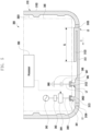
- the antenna 370 may be disposed between the rear plate 380 and the battery 350.
- the antenna 370 may include, for example, a near field communication (NFC) antenna, a wireless charging antenna, and/or a magnetic secure transmission (MST) antenna.
- NFC near field communication
- MST magnetic secure transmission
- the antenna 370 may perform short-range communication with an external device, or transmit and receive power required for charging wirelessly.
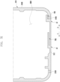
- An antenna structure may be formed by a part or combination of the lateral bezel structure 310 and/or the first support member 311.
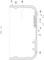
- the first housing structure 810 may have a first surface 811 facing in a first direction, a second surface 812 facing in a second direction opposite to the first direction, and a first lateral member 813 (e.g., a first lateral frame or a first lateral bezel) surrounding at least a part of a space between the first surface 811 and the second surface 812.
- a first lateral member 813 e.g., a first lateral frame or a first lateral bezel
- at least a part of the first lateral member 813 may be formed of a conductive member (e.g., a metal member).
- at least a part of the first lateral member 813 formed of the conductive member may be applied as an antenna A1.
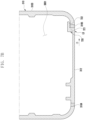
- the second housing structure 820 may have a third surface 821 facing in a third direction, a fourth surface 822 facing in a fourth direction opposite to the third direction, and a second lateral member 823 (e.g., a second lateral frame or a second lateral bezel) surrounding at least a part of a space between the third surface 821 and the fourth surface 822.
- a second lateral member 823 e.g., a second lateral frame or a second lateral bezel
- the electronic device 800 may include a display 830 (e.g., a touch-type flexible display) disposed to cross the first surface 811 of the first housing structure 810 and the third surface 821 of the second housing structure 820.
- a display 830 e.g., a touch-type flexible display
- the display 830 may also be folded to face each other based on the folding axis X.
- the display 830 may not be disposed and a separate sensor region 835 may be disposed.
- the sensor region 835 e.g., a notch region
- the sensor region 835 may be disposed on at least a part of the third surface 821 of the second housing structure 820, or may be disposed to extend to the first surface 811 and the third surface 821.
- the conductive portion 8131 used as an antenna may be formed using a part (e.g., a lower region) of the first lateral member 813 of the first housing structure 810. In another embodiment, the conductive portion 8131 may be disposed in an upper region of the first housing structure 810 or in a lateral region connecting the upper region and the lower region.
- the conductive portion 8131 may include a conductive extended portion (e.g., a conductive extended portion 8132 in FIG. 10 ) having a predetermined electrical length extended in a direction toward the inner space of the first housing structure 810.
- the antenna A1 may be configured to operate in a desired frequency band while coping with the slimming of the first housing structure 810.
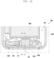
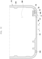
- FIG. 10 is a diagram illustrating the arrangement of an antenna in the foldable electronic device of FIG. 8 according to an embodiment of the disclosure.
- the first housing structure 810 of the electronic device 800 may include the first lateral member 813.
- the first lateral member 813 may have a first connection piece 814 formed at a first location L1 of the conductive portion 8131 from the first non-conductive portion 8101, and a second connection piece 815 formed at a second location L2.
- the first location L1 may be disposed closer to the first non-conductive portion 8101 than the second location L2.
- the first location L1 may be disposed farther from the first non-conductive portion 8101 than the second location L2.
- the first connection piece 814 and the second connection piece 815 may be integrally formed with the conductive portion 8131.
- the first connection piece 814 and the second connection piece 815 may be disposed to be overlapped with at least a part of the printed circuit board 840 disposed in at least a part of the inner space 8001 of the first housing structure 810.
- the electronic device 800 may include the printed circuit board 840 disposed in the inner space 8001 of the first housing structure 810.
- the printed circuit board 840 may include a first connection part 841 (e.g., a conductive pad) electrically connected to the first connection piece 814.
- the printed circuit board 840 may include a first electrical path 8401 (e.g., a wiring line) connected from the first connection piece 814 to a power feeder 842 (e.g., a wireless communication circuit).
- the power feeder 842 may transmit a signal of a desired frequency band at the first location L1 of the conductive portion 8131 electrically connected through the first electrical path 8401.
- the printed circuit board 840 may include a second connection part 845 (e.g., a conductive pad) electrically connected to the second connection piece 815.
- the printed circuit board 840 may include a second electrical path 8402 (e.g., a wiring line) connected from the second connection part 845 to a ground (GND) 846 of the printed circuit board 840.
- the printed circuit board 840 may include at least one electric shock protection capacitor 847 disposed on the second electrical path 8402.
- the conductive portion 8131 may include the conductive extended portion 8132 extended from a third location L3 of the end contacting the second non-conductive portion 8102 toward the inner space 8001 of the first housing structure 810.
- the conductive extended portion 8132 may be extended from the end of the conductive portion 8131 in a direction (direction 1) toward the first non-conductive portion 8101 in parallel or non-parallel with the conductive portion 8131.
- the conductive portion 8131 electrically connected to the power feeder 842 may have an electrical length including the conductive extended portion 8132 extended at a certain length from the end, and may be determined to operate in a desired operating frequency band.
- the corresponding frequency band may have a range of about 850 MHz to 3000 MHz.
- the conductive extended portion 8132 when the first surface (e.g., the first surface 811 in FIG. 8 ) is viewed from above, at least a part of the conductive extended portion 8132 may be disposed so as not to be overlapped with the printed circuit board 840. In another embodiment, when the first surface (e.g., the first surface 811 in FIG. 8 ) is viewed from above, at least a part of the conductive extended portion 8132 may be disposed so as to be overlapped with the printed circuit board 840. In this case, in order to prevent signal distortion and/or radiation performance degradation due to surrounding conductors, a region of the printed circuit board 840 overlapped with the conductive extended portion 8132 may be formed as a non-conductive region.
- the conductive extended portion 8132 extended from the conductive portion 8131 may be replaced with at least one of the above-described conductive extended portions 710, 720, 730, and 740 in FIGS. 7A to 7E .
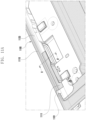
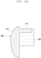
- FIG. 11A is a perspective view partially illustrating a lateral member 1100 in which a conductive portion 1110 and a polymer portion 1120 are insert-injected according to an embodiment of the disclosure.
- FIG. 11B is a cross-sectional view taken along the line B-B' of FIG. 11A according to an embodiment of the disclosure.
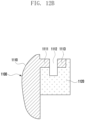
- FIG. 12A is a perspective view partially illustrating a state where a conductive extended portion 1113 is formed in a lateral member 1100 according to an embodiment of the disclosure.
- FIG. 12B is a cross-sectional view taken along the line C-C' of FIG. 12A according to an embodiment of the disclosure.
- the above-described conductive extended portion (e.g., the conductive extended portion 3123 in FIG. 5 ) should be formed with a slit that is quite narrow from the conductive portion (e.g., the conductive portion 312 in FIG. 5 ), and should avoid surrounding electronic components (e.g., a USB connector). Therefore, only the insert injection process for the conductive portion and the polymer portion may not completely fill the slit with a polymer member, which may result in a shape defect of the conductive extended portion.
- the conductive extended portion 1113 e.g., the conductive extended portion 3123 in FIG. 5 .
- the conductive extension dummy 1111 insert-injected into the polymer portion 1120 may be cut at least in part to have a predetermined width in a longitudinal direction parallel with the conductive portion 1110, thus resultantly forming the conductive extended portion 1113.
- the conductive extension dummy 1111 may be cut through a milling machine or an NC machine.
- the conductive extension dummy 1111 may be cut to a depth that is greater than the thickness of the conductive extension dummy 1111, so that an electrical isolation state from the conductive portion 1110 may be maintained by a cut portion 1112 except for a portion intentionally connected to the conductive portion 1110.
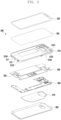
- an electronic device e.g., the electronic device 300 in FIG. 3
- a housing e.g., the housing 210 in FIG. 2A
- a front plate e.g., the front plate 320 in FIG. 3
- a rear plate e.g., the rear plate 380 in FIG. 3
- a lateral member e.g., the lateral member 310 in FIG. 3
- at least a part of the lateral member includes at least one conductive portion (e.g., the conductive portion 312 in FIG.
- a first non-conductive portion e.g., the first non-conductive portion 3104 in FIG. 5
- a second non-conductive portion e.g., the second non-conductive portion 3105 in FIG. 5
- a conductive extended portion e.g., the conductive extended portion 2123 in FIG. 5
- a printed circuit board e.g., the printed circuit board 340 in FIG. 5
- a wireless communication circuit e.g., the power feeder 342 in FIG. 5
- a first location e.g., the first location L1 in FIG. 5
- the printed circuit board may include a ground (GND), and the first location of the conductive portion may be electrically connected to the ground.
- GND ground
- the printed circuit board may include a ground (GND) (e.g., the ground 346 in FIG. 5 ), and the conductive portion may be electrically connected to the ground at a second location (e.g., the second location L2 in FIG. 5 ) farther from the first non-conductive portion than the first location.
- GND ground
- the conductive portion may be electrically connected to the ground at a second location (e.g., the second location L2 in FIG. 5 ) farther from the first non-conductive portion than the first location.
- the conductive extended portion may be extended into the space from an end (e.g., the third location L3 in FIG. 5 ) of the conductive portion in contact with the second non-conductive portion.
- the conductive extended portion may be extended to have a predetermined electrical length (e.g., the electrical length EL in FIG. 5 ) and a predetermined interval in parallel with the conductive portion in the space.
- a predetermined electrical length e.g., the electrical length EL in FIG. 5
- a predetermined interval in parallel with the conductive portion in the space.
- the conductive extended portion may be extended from the conductive portion in a direction toward the second non-conductive portion.
- the conductive extended portion may be disposed so as not to be overlapped with the printed circuit board when the front plate is viewed from above.
- the conductive extended portion may be disposed so as to be overlapped, at least in part, with the printed circuit board when the front plate is viewed from above.
- a region of the printed circuit board overlapped with the conductive extended portion may be formed as a non-conductive region.
- the conductive extended portion may be branched in a direction toward the space between (e.g., at the fourth location L4 in FIG. 7D ) the first location of the conductive portion and the second non-conductive portion.
- the wireless communication circuit may be configured to transmit and/or receive a signal of at least one frequency band in a range of about 850 MHz to 3000 MHz through the conductive portion and the conductive extended portion.
- the electronic device may further include a display (e.g., the display 330 in FIG. 3 ) disposed in the space and disposed to be visible from an outside through at least a part of the front plate.
- a display e.g., the display 330 in FIG. 3
- the wireless communication circuit may be configured to transmit and/or receive a signal of at least one frequency band in a range of about 850 MHz to 3000 MHz through the conductive portion and the conductive extended portion.
Landscapes
- Engineering & Computer Science (AREA)
- Signal Processing (AREA)
- Computer Networks & Wireless Communication (AREA)
- Microelectronics & Electronic Packaging (AREA)
- Telephone Set Structure (AREA)
Claims (12)
- Elektronische Vorrichtung (300), die Folgendes umfasst:ein Gehäuse (210), das Folgendes enthält:eine Frontplatte (320),eine Rückplatte (380), die in eine der Frontplatte (320) entgegengesetzte Richtung gerichtet ist,ein Seitenelement (310), das einen Raum (3001) zwischen der Frontplatte (320) und der Rückplatte (380) umgibt, wobei zumindest ein Teil des Seitenelements (310) zumindest einen leitenden Abschnitt (312) enthält, der zwischen einem ersten nicht-leitenden Abschnitt (3104) und einem zweiten nicht-leitenden Abschnitt (3105), die voneinander beabstandet sind, angeordnet ist, und
ein Stützelement (311), das sich von dem Seitenelement (310) in Richtung des Raums (3001) erstreckt und ein leitendes Teil und ein Polymerteil (313) enthält, die durch Einspritzen in einen Körper mit dem leitenden Teil gebildet werden;einen sich erstreckenden leitenden Abschnitt (3123), der sich einstückig von zumindest einem Teil des leitenden Abschnitts (312) zu dem Raum (3001) zwischen der Frontplatte (320) und der Rückplatte (380) erstreckt;eine Leiterplatte (340), die in dem Raum zwischen der Frontplatte (320) und der Rückplatte (340) angeordnet ist; undeine drahtlose Kommunikationsschaltung (342), die auf der Leiterplatte angeordnet und elektrisch mit dem leitenden Abschnitt an einer ersten Stelle (L1) des leitenden Abschnitts (312) verbunden ist, die von dem ersten nicht-leitenden Abschnitt (3104) beabstandet ist,wobei sich der erste nicht-leitende Abschnitt (3104) und der zweite nicht-leitende Abschnitt (3105) von dem Polymerteil (313) aus erstrecken, wobei der erste nicht-leitende Abschnitt (3104), der zweite nicht-leitende Abschnitt (3105) und der Polymerteil (313) zusammen durch ein Einspritzverfahren gebildet werden, undwobei der sich erstreckende leitende Abschnitt (3123) gestützt wird, indem er zusammen mit dem Polymerteil (313) durch Einspritzen in den Raum (3001) eingeführt wird. - Elektronische Vorrichtung nach Anspruch 1,wobei die Leiterplatte (340) eine Masse (GND) enthält, undwobei die erste Stelle (L1) des leitenden Abschnitts (312) elektrisch mit der Masse (GND) verbunden ist.
- Elektronische Vorrichtung nach Anspruch 1,wobei die Leiterplatte (340) eine Masse (GND) enthält, undwobei der leitende Abschnitt (312) an einer zweiten Stelle (L2), die weiter von dem ersten nicht-leitenden Abschnitt (3104) entfernt ist als die erste Stelle (L1), elektrisch mit der Masse (GND) verbunden ist.
- Elektronische Vorrichtung nach Anspruch 1, wobei der sich erstreckende leitende Abschnitt (3123) sich in den Raum (3001) zwischen der Frontplatte (320) und der Rückplatte (380) in Kontakt mit dem zweiten nicht-leitenden Abschnitt (3105) von einem Ende des leitenden Abschnitts (312) aus erstreckt.
- Elektronische Vorrichtung nach Anspruch 4, wobei der sich erstreckende leitende Abschnitt (3123) sich so erstreckt, dass er eine vorbestimmte elektrische Länge (EL) und einen vorbestimmten Abstand parallel zu dem leitenden Abschnitt (312) in dem Raum (3001) zwischen der Frontplatte (320) und der Rückplatte (380) aufweist.
- Elektronische Vorrichtung nach Anspruch 4, wobei der sich erstreckende leitende Abschnitt (3123) sich von dem leitenden Abschnitt (312) in eine Richtung zu dem zweiten nicht-leitenden Abschnitt (3105) erstreckt.
- Elektronische Vorrichtung nach Anspruch 1, wobei der sich erstreckende leitende Abschnitt (3123) so angeordnet ist, dass er sich nicht mit der Leiterplatte (340) überlappt, wenn die Frontplatte (320) von oben betrachtet wird.
- Elektronische Vorrichtung nach Anspruch 1, wobei der sich erstreckende leitende Abschnitt (3123) so angeordnet ist, dass er sich zumindest zum Teil mit der Leiterplatte (340) überlappt, wenn die Frontplatte (320) von oben betrachtet wird.
- Elektronische Vorrichtung nach Anspruch 8, wobei ein Bereich der Leiterplatte (340), der sich mit dem sich erstreckenden leitenden Abschnitt (3123) überlappt, als ein nicht-leitender Bereich gebildet ist.
- Elektronische Vorrichtung nach Anspruch 1, wobei der sich erstreckende leitende Abschnitt (3123) sich in Richtung zu dem Raum (3001) zwischen der Frontplatte (320) und der Rückplatte (380) zwischen der ersten Stelle (L1) des leitenden Abschnitts (314) und dem zweiten nicht-leitenden Abschnitt (3105) verzweigt.
- Elektronische Vorrichtung nach Anspruch 1, wobei die drahtlose Kommunikationsschaltung (342) so konfiguriert ist, dass sie über den leitenden Abschnitt (312) und den sich erstreckenden leitenden Abschnitt (3123) ein Signal von mindestens einem Frequenzband in einem Bereich von etwa 850 Megahertz (MHz) bis 3000 MHz sendet und/oder empfängt.
- Elektronische Vorrichtung nach Anspruch 1, die ferner Folgendes umfasst:
eine Anzeige (330), die in dem Raum (3001) zwischen der Frontplatte (320) und der Rückplatte (380) angeordnet ist und so angeordnet ist, dass sie von außen durch zumindest einen Teil der Frontplatte (320) hindurch sichtbar ist.
Applications Claiming Priority (2)
| Application Number | Priority Date | Filing Date | Title |
|---|---|---|---|
| KR1020190016491A KR102613216B1 (ko) | 2019-02-13 | 2019-02-13 | 안테나 및 그것을 포함하는 전자 장치 |
| PCT/KR2020/000028 WO2020166821A1 (ko) | 2019-02-13 | 2020-01-02 | 안테나 및 그것을 포함하는 전자 장치 |
Publications (3)
| Publication Number | Publication Date |
|---|---|
| EP3910918A1 EP3910918A1 (de) | 2021-11-17 |
| EP3910918A4 EP3910918A4 (de) | 2022-06-15 |
| EP3910918B1 true EP3910918B1 (de) | 2025-06-25 |
Family
ID=72043930
Family Applications (1)
| Application Number | Title | Priority Date | Filing Date |
|---|---|---|---|
| EP20755747.1A Active EP3910918B1 (de) | 2019-02-13 | 2020-01-02 | Antenne und elektronische vorrichtung damit |
Country Status (5)
| Country | Link |
|---|---|
| US (1) | US12041191B2 (de) |
| EP (1) | EP3910918B1 (de) |
| KR (1) | KR102613216B1 (de) |
| CN (1) | CN113439432B (de) |
| WO (1) | WO2020166821A1 (de) |
Families Citing this family (11)
| Publication number | Priority date | Publication date | Assignee | Title |
|---|---|---|---|---|
| KR102518499B1 (ko) * | 2016-04-22 | 2023-04-05 | 삼성전자주식회사 | 안테나 및 이를 포함하는 전자 장치 |
| KR102768563B1 (ko) * | 2020-07-13 | 2025-02-17 | 삼성전자주식회사 | 안테나 모듈 및 이를 포함하는 전자 장치 |
| KR102758022B1 (ko) * | 2020-09-24 | 2025-01-21 | 삼성전자주식회사 | 안테나 및 이를 구비한 전자 장치 |
| CN116324946A (zh) | 2020-11-06 | 2023-06-23 | 三星电子株式会社 | 包括柔性显示器的电子装置 |
| KR20220080544A (ko) * | 2020-12-07 | 2022-06-14 | 삼성전자주식회사 | 안테나를 포함하는 전자 장치 및 그 제조 방법 |
| KR20220141120A (ko) * | 2021-04-12 | 2022-10-19 | 삼성전자주식회사 | 안테나 및 그것을 포함하는 전자 장치 |
| EP4246715A4 (de) | 2021-04-12 | 2024-07-03 | Samsung Electronics Co., Ltd. | Antenne und elektronische vorrichtung damit |
| KR102845136B1 (ko) | 2021-04-22 | 2025-08-12 | 삼성전자주식회사 | 방사 성능 향상을 위한 안테나 구조 및 이를 포함하는 전자 장치 |
| KR20230024758A (ko) * | 2021-08-12 | 2023-02-21 | 삼성전자주식회사 | 안테나를 포함하는 모바일 통신 장치 |
| KR20230027914A (ko) | 2021-08-20 | 2023-02-28 | 삼성전자주식회사 | 안테나를 포함하는 전자 장치 |
| CN118232005B (zh) * | 2023-06-21 | 2025-07-08 | 华为技术有限公司 | 一种可折叠电子设备 |
Family Cites Families (22)
| Publication number | Priority date | Publication date | Assignee | Title |
|---|---|---|---|---|
| KR101709532B1 (ko) * | 2010-11-11 | 2017-02-24 | 엘지전자 주식회사 | 이동 단말기 |
| KR101801186B1 (ko) * | 2011-02-25 | 2017-11-24 | 엘지전자 주식회사 | 이동 단말기 |
| JP2013197852A (ja) * | 2012-03-19 | 2013-09-30 | Panasonic Corp | 携帯無線端末用ケース |
| CN103236583B (zh) | 2013-04-25 | 2016-06-08 | 上海安费诺永亿通讯电子有限公司 | 一种增强带宽的新型lte金属框天线 |
| CN103296385B (zh) | 2013-05-29 | 2016-05-11 | 上海安费诺永亿通讯电子有限公司 | 一种可调式多频天线系统 |
| CN104681929B (zh) | 2013-11-30 | 2019-05-21 | 深圳富泰宏精密工业有限公司 | 天线结构及具有该天线结构的无线通信装置 |
| CN104752824B (zh) | 2013-12-30 | 2019-06-18 | 深圳富泰宏精密工业有限公司 | 天线结构及应用该天线结构的无线通信装置 |
| KR101580546B1 (ko) * | 2014-07-02 | 2015-12-31 | 김우중 | 금속 테두리를 갖는 이동통신 단말기용 안테나 및 이를 갖는 이동통신 단말기 |
| KR102364605B1 (ko) | 2015-05-27 | 2022-02-21 | 삼성전자주식회사 | 다중 대역 안테나 및 이를 포함하는 전자 장치 |
| CN104852122A (zh) * | 2015-06-09 | 2015-08-19 | 联想(北京)有限公司 | 电子设备和天线装置 |
| CN107026314B (zh) * | 2016-01-29 | 2020-02-07 | 北京小米移动软件有限公司 | 移动终端的天线 |
| KR102466002B1 (ko) * | 2016-04-19 | 2022-11-11 | 삼성전자주식회사 | 안테나를 포함하는 전자 장치 |
| KR102518499B1 (ko) * | 2016-04-22 | 2023-04-05 | 삼성전자주식회사 | 안테나 및 이를 포함하는 전자 장치 |
| KR101832147B1 (ko) * | 2016-05-26 | 2018-02-26 | (주)파트론 | 안테나 장치 |
| KR102465796B1 (ko) * | 2016-05-27 | 2022-11-10 | 삼성전자주식회사 | 다중 슬롯 안테나를 가지는 전자 장치 |
| CN106102389B (zh) * | 2016-08-16 | 2018-05-29 | 广东欧珀移动通信有限公司 | 一种壳体的加工方法、壳体和移动终端 |
| CN108123210B (zh) | 2016-11-26 | 2020-07-28 | 北京小米移动软件有限公司 | 终端的天线 |
| KR102586064B1 (ko) * | 2017-02-16 | 2023-10-05 | 엘에스엠트론 주식회사 | 안테나 장치 |
| KR102441838B1 (ko) * | 2018-02-14 | 2022-09-08 | 삼성전자주식회사 | 브라켓의 개구부에서 발생되는 공진을 조정하기 위해 개구부에 전기적으로 연결된 도전성 부재를 포함하는 전자 장치 |
| KR102482071B1 (ko) * | 2018-02-14 | 2022-12-28 | 삼성전자주식회사 | 다중 급전을 이용한 안테나 및 그것을 포함하는 전자 장치 |
| KR102487375B1 (ko) * | 2018-05-04 | 2023-01-11 | 삼성전자주식회사 | 안테나 및 그것을 포함하는 전자 장치 |
| US11189909B2 (en) * | 2018-08-30 | 2021-11-30 | Apple Inc. | Housing and antenna architecture for mobile device |
-
2019
- 2019-02-13 KR KR1020190016491A patent/KR102613216B1/ko active Active
-
2020
- 2020-01-02 US US17/426,892 patent/US12041191B2/en active Active
- 2020-01-02 CN CN202080014850.0A patent/CN113439432B/zh active Active
- 2020-01-02 EP EP20755747.1A patent/EP3910918B1/de active Active
- 2020-01-02 WO PCT/KR2020/000028 patent/WO2020166821A1/ko not_active Ceased
Also Published As
| Publication number | Publication date |
|---|---|
| CN113439432B (zh) | 2024-11-08 |
| CN113439432A (zh) | 2021-09-24 |
| KR102613216B1 (ko) | 2023-12-13 |
| KR20200098857A (ko) | 2020-08-21 |
| EP3910918A4 (de) | 2022-06-15 |
| EP3910918A1 (de) | 2021-11-17 |
| WO2020166821A1 (ko) | 2020-08-20 |
| US20220103668A1 (en) | 2022-03-31 |
| US12041191B2 (en) | 2024-07-16 |
Similar Documents
| Publication | Publication Date | Title |
|---|---|---|
| EP3910918B1 (de) | Antenne und elektronische vorrichtung damit | |
| US12327911B2 (en) | Antenna and electronic device comprising same | |
| US11246229B2 (en) | Electronic component arrangement structure and electronic device including same | |
| US11569561B2 (en) | Antenna having single non-conductive portion and electronic device including the same | |
| KR102562631B1 (ko) | 안테나 및 그것을 포함하는 전자 장치 | |
| US10833403B2 (en) | Antenna and electronic device including same | |
| EP4142050A1 (de) | Elektronische vorrichtung mit antenne | |
| KR102441838B1 (ko) | 브라켓의 개구부에서 발생되는 공진을 조정하기 위해 개구부에 전기적으로 연결된 도전성 부재를 포함하는 전자 장치 | |
| US11522271B2 (en) | Antenna and electronic device comprising same | |
| KR20200099417A (ko) | 안테나 모듈 및 이를 포함하는 전자 장치 | |
| US12548884B2 (en) | Antenna and electronic apparatus including the same | |
| US11546454B2 (en) | Electronic device including connector mounted on circuit board | |
| KR102352491B1 (ko) | 안테나 및 안테나를 포함하는 전자 장치 | |
| KR102664682B1 (ko) | 도전성 측면 부재를 이용한 안테나 및 그것을 포함하는 전자 장치 | |
| KR20210061859A (ko) | 고립된 도전체를 포함하는 전자 장치 | |
| CN111670414A (zh) | 使用多馈电天线的天线以及包括该天线的电子装置 | |
| KR102457138B1 (ko) | 커넥터를 포함하는 전자 장치 | |
| US11563280B2 (en) | Electronic device including antenna | |
| KR102765441B1 (ko) | 그립 감지 방법 및 이를 지원하는 전자 장치 | |
| KR20210115192A (ko) | 안테나 및 그립 센서를 포함하는 전자 장치 | |
| EP4325821A1 (de) | Elektronische vorrichtung mit antenne und mikrofon |
Legal Events
| Date | Code | Title | Description |
|---|---|---|---|
| STAA | Information on the status of an ep patent application or granted ep patent |
Free format text: STATUS: THE INTERNATIONAL PUBLICATION HAS BEEN MADE |
|
| PUAI | Public reference made under article 153(3) epc to a published international application that has entered the european phase |
Free format text: ORIGINAL CODE: 0009012 |
|
| STAA | Information on the status of an ep patent application or granted ep patent |
Free format text: STATUS: REQUEST FOR EXAMINATION WAS MADE |
|
| 17P | Request for examination filed |
Effective date: 20210811 |
|
| AK | Designated contracting states |
Kind code of ref document: A1 Designated state(s): AL AT BE BG CH CY CZ DE DK EE ES FI FR GB GR HR HU IE IS IT LI LT LU LV MC MK MT NL NO PL PT RO RS SE SI SK SM TR |
|
| RIC1 | Information provided on ipc code assigned before grant |
Ipc: H01Q 9/42 20060101ALI20220201BHEP Ipc: H01Q 5/335 20150101ALI20220201BHEP Ipc: H01Q 1/44 20060101ALI20220201BHEP Ipc: H04B 1/40 20150101ALI20220201BHEP Ipc: H01Q 1/24 20060101ALI20220201BHEP Ipc: H04M 1/02 20060101AFI20220201BHEP |
|
| DAV | Request for validation of the european patent (deleted) | ||
| DAX | Request for extension of the european patent (deleted) | ||
| A4 | Supplementary search report drawn up and despatched |
Effective date: 20220512 |
|
| RIC1 | Information provided on ipc code assigned before grant |
Ipc: H01Q 9/42 20060101ALI20220506BHEP Ipc: H01Q 5/335 20150101ALI20220506BHEP Ipc: H01Q 1/44 20060101ALI20220506BHEP Ipc: H04B 1/40 20150101ALI20220506BHEP Ipc: H01Q 1/24 20060101ALI20220506BHEP Ipc: H04M 1/02 20060101AFI20220506BHEP |
|
| STAA | Information on the status of an ep patent application or granted ep patent |
Free format text: STATUS: EXAMINATION IS IN PROGRESS |
|
| 17Q | First examination report despatched |
Effective date: 20230530 |
|
| REG | Reference to a national code |
Ref country code: DE Free format text: PREVIOUS MAIN CLASS: H04M0001020000 Ref country code: DE Ref legal event code: R079 Ref document number: 602020053342 Country of ref document: DE Free format text: PREVIOUS MAIN CLASS: H04M0001020000 Ipc: H01Q0001240000 |
|
| GRAP | Despatch of communication of intention to grant a patent |
Free format text: ORIGINAL CODE: EPIDOSNIGR1 |
|
| RIC1 | Information provided on ipc code assigned before grant |
Ipc: H01Q 5/371 20150101ALN20250107BHEP Ipc: H04M 1/02 20060101ALI20250107BHEP Ipc: H04B 1/40 20150101ALI20250107BHEP Ipc: H01Q 9/42 20060101ALI20250107BHEP Ipc: H01Q 5/335 20150101ALI20250107BHEP Ipc: H01Q 1/44 20060101ALI20250107BHEP Ipc: H01Q 1/24 20060101AFI20250107BHEP |
|
| STAA | Information on the status of an ep patent application or granted ep patent |
Free format text: STATUS: GRANT OF PATENT IS INTENDED |
|
| RIC1 | Information provided on ipc code assigned before grant |
Ipc: H01Q 5/371 20150101ALN20250129BHEP Ipc: H04M 1/02 20060101ALI20250129BHEP Ipc: H04B 1/40 20150101ALI20250129BHEP Ipc: H01Q 9/42 20060101ALI20250129BHEP Ipc: H01Q 5/335 20150101ALI20250129BHEP Ipc: H01Q 1/44 20060101ALI20250129BHEP Ipc: H01Q 1/24 20060101AFI20250129BHEP |
|
| INTG | Intention to grant announced |
Effective date: 20250213 |
|
| GRAS | Grant fee paid |
Free format text: ORIGINAL CODE: EPIDOSNIGR3 |
|
| GRAA | (expected) grant |
Free format text: ORIGINAL CODE: 0009210 |
|
| STAA | Information on the status of an ep patent application or granted ep patent |
Free format text: STATUS: THE PATENT HAS BEEN GRANTED |
|
| AK | Designated contracting states |
Kind code of ref document: B1 Designated state(s): AL AT BE BG CH CY CZ DE DK EE ES FI FR GB GR HR HU IE IS IT LI LT LU LV MC MK MT NL NO PL PT RO RS SE SI SK SM TR |
|
| REG | Reference to a national code |
Ref country code: GB Ref legal event code: FG4D |
|
| REG | Reference to a national code |
Ref country code: CH Ref legal event code: EP |
|
| REG | Reference to a national code |
Ref country code: CH Ref legal event code: EP |
|
| REG | Reference to a national code |
Ref country code: IE Ref legal event code: FG4D |
|
| REG | Reference to a national code |
Ref country code: DE Ref legal event code: R096 Ref document number: 602020053342 Country of ref document: DE |
|
| PG25 | Lapsed in a contracting state [announced via postgrant information from national office to epo] |
Ref country code: FI Free format text: LAPSE BECAUSE OF FAILURE TO SUBMIT A TRANSLATION OF THE DESCRIPTION OR TO PAY THE FEE WITHIN THE PRESCRIBED TIME-LIMIT Effective date: 20250625 |
|
| REG | Reference to a national code |
Ref country code: LT Ref legal event code: MG9D |
|
| PG25 | Lapsed in a contracting state [announced via postgrant information from national office to epo] |
Ref country code: GR Free format text: LAPSE BECAUSE OF FAILURE TO SUBMIT A TRANSLATION OF THE DESCRIPTION OR TO PAY THE FEE WITHIN THE PRESCRIBED TIME-LIMIT Effective date: 20250926 Ref country code: NO Free format text: LAPSE BECAUSE OF FAILURE TO SUBMIT A TRANSLATION OF THE DESCRIPTION OR TO PAY THE FEE WITHIN THE PRESCRIBED TIME-LIMIT Effective date: 20250925 |
|
| PG25 | Lapsed in a contracting state [announced via postgrant information from national office to epo] |
Ref country code: BG Free format text: LAPSE BECAUSE OF FAILURE TO SUBMIT A TRANSLATION OF THE DESCRIPTION OR TO PAY THE FEE WITHIN THE PRESCRIBED TIME-LIMIT Effective date: 20250625 |
|
| PG25 | Lapsed in a contracting state [announced via postgrant information from national office to epo] |
Ref country code: HR Free format text: LAPSE BECAUSE OF FAILURE TO SUBMIT A TRANSLATION OF THE DESCRIPTION OR TO PAY THE FEE WITHIN THE PRESCRIBED TIME-LIMIT Effective date: 20250625 |
|
| PG25 | Lapsed in a contracting state [announced via postgrant information from national office to epo] |
Ref country code: RS Free format text: LAPSE BECAUSE OF FAILURE TO SUBMIT A TRANSLATION OF THE DESCRIPTION OR TO PAY THE FEE WITHIN THE PRESCRIBED TIME-LIMIT Effective date: 20250925 |
|
| PG25 | Lapsed in a contracting state [announced via postgrant information from national office to epo] |
Ref country code: LV Free format text: LAPSE BECAUSE OF FAILURE TO SUBMIT A TRANSLATION OF THE DESCRIPTION OR TO PAY THE FEE WITHIN THE PRESCRIBED TIME-LIMIT Effective date: 20250625 |
|
| REG | Reference to a national code |
Ref country code: NL Ref legal event code: MP Effective date: 20250625 |
|
| PG25 | Lapsed in a contracting state [announced via postgrant information from national office to epo] |
Ref country code: NL Free format text: LAPSE BECAUSE OF FAILURE TO SUBMIT A TRANSLATION OF THE DESCRIPTION OR TO PAY THE FEE WITHIN THE PRESCRIBED TIME-LIMIT Effective date: 20250625 |
|
| PG25 | Lapsed in a contracting state [announced via postgrant information from national office to epo] |
Ref country code: PT Free format text: LAPSE BECAUSE OF FAILURE TO SUBMIT A TRANSLATION OF THE DESCRIPTION OR TO PAY THE FEE WITHIN THE PRESCRIBED TIME-LIMIT Effective date: 20251027 |
|
| REG | Reference to a national code |
Ref country code: AT Ref legal event code: MK05 Ref document number: 1807573 Country of ref document: AT Kind code of ref document: T Effective date: 20250625 |
|
| PG25 | Lapsed in a contracting state [announced via postgrant information from national office to epo] |
Ref country code: IS Free format text: LAPSE BECAUSE OF FAILURE TO SUBMIT A TRANSLATION OF THE DESCRIPTION OR TO PAY THE FEE WITHIN THE PRESCRIBED TIME-LIMIT Effective date: 20251025 |
|
| PG25 | Lapsed in a contracting state [announced via postgrant information from national office to epo] |
Ref country code: AT Free format text: LAPSE BECAUSE OF FAILURE TO SUBMIT A TRANSLATION OF THE DESCRIPTION OR TO PAY THE FEE WITHIN THE PRESCRIBED TIME-LIMIT Effective date: 20250625 Ref country code: SM Free format text: LAPSE BECAUSE OF FAILURE TO SUBMIT A TRANSLATION OF THE DESCRIPTION OR TO PAY THE FEE WITHIN THE PRESCRIBED TIME-LIMIT Effective date: 20250625 |
|
| PG25 | Lapsed in a contracting state [announced via postgrant information from national office to epo] |
Ref country code: CZ Free format text: LAPSE BECAUSE OF FAILURE TO SUBMIT A TRANSLATION OF THE DESCRIPTION OR TO PAY THE FEE WITHIN THE PRESCRIBED TIME-LIMIT Effective date: 20250625 |
|
| PG25 | Lapsed in a contracting state [announced via postgrant information from national office to epo] |
Ref country code: PL Free format text: LAPSE BECAUSE OF FAILURE TO SUBMIT A TRANSLATION OF THE DESCRIPTION OR TO PAY THE FEE WITHIN THE PRESCRIBED TIME-LIMIT Effective date: 20250625 |
|
| PG25 | Lapsed in a contracting state [announced via postgrant information from national office to epo] |
Ref country code: EE Free format text: LAPSE BECAUSE OF FAILURE TO SUBMIT A TRANSLATION OF THE DESCRIPTION OR TO PAY THE FEE WITHIN THE PRESCRIBED TIME-LIMIT Effective date: 20250625 |
|
| PG25 | Lapsed in a contracting state [announced via postgrant information from national office to epo] |
Ref country code: SK Free format text: LAPSE BECAUSE OF FAILURE TO SUBMIT A TRANSLATION OF THE DESCRIPTION OR TO PAY THE FEE WITHIN THE PRESCRIBED TIME-LIMIT Effective date: 20250625 |
|
| PG25 | Lapsed in a contracting state [announced via postgrant information from national office to epo] |
Ref country code: ES Free format text: LAPSE BECAUSE OF FAILURE TO SUBMIT A TRANSLATION OF THE DESCRIPTION OR TO PAY THE FEE WITHIN THE PRESCRIBED TIME-LIMIT Effective date: 20250625 |