EP3907738B1 - Semiconductor memory with detection of address circuit failures - Google Patents
Semiconductor memory with detection of address circuit failures Download PDFInfo
- Publication number
- EP3907738B1 EP3907738B1 EP21154726.0A EP21154726A EP3907738B1 EP 3907738 B1 EP3907738 B1 EP 3907738B1 EP 21154726 A EP21154726 A EP 21154726A EP 3907738 B1 EP3907738 B1 EP 3907738B1
- Authority
- EP
- European Patent Office
- Prior art keywords
- address information
- column
- row
- level
- circuit
- Prior art date
- Legal status (The legal status is an assumption and is not a legal conclusion. Google has not performed a legal analysis and makes no representation as to the accuracy of the status listed.)
- Active
Links
Images


Classifications
-
- G—PHYSICS
- G11—INFORMATION STORAGE
- G11C—STATIC STORES
- G11C29/00—Checking stores for correct operation ; Subsequent repair; Testing stores during standby or offline operation
- G11C29/04—Detection or location of defective memory elements, e.g. cell constructio details, timing of test signals
- G11C29/08—Functional testing, e.g. testing during refresh, power-on self testing [POST] or distributed testing
- G11C29/12—Built-in arrangements for testing, e.g. built-in self testing [BIST] or interconnection details
- G11C29/38—Response verification devices
- G11C29/42—Response verification devices using error correcting codes [ECC] or parity check
-
- G—PHYSICS
- G11—INFORMATION STORAGE
- G11C—STATIC STORES
- G11C29/00—Checking stores for correct operation ; Subsequent repair; Testing stores during standby or offline operation
- G11C29/04—Detection or location of defective memory elements, e.g. cell constructio details, timing of test signals
- G11C29/08—Functional testing, e.g. testing during refresh, power-on self testing [POST] or distributed testing
- G11C29/12—Built-in arrangements for testing, e.g. built-in self testing [BIST] or interconnection details
- G11C29/18—Address generation devices; Devices for accessing memories, e.g. details of addressing circuits
-
- G—PHYSICS
- G11—INFORMATION STORAGE
- G11C—STATIC STORES
- G11C8/00—Arrangements for selecting an address in a digital store
- G11C8/10—Decoders
-
- G—PHYSICS
- G11—INFORMATION STORAGE
- G11C—STATIC STORES
- G11C29/00—Checking stores for correct operation ; Subsequent repair; Testing stores during standby or offline operation
- G11C29/02—Detection or location of defective auxiliary circuits, e.g. defective refresh counters
- G11C29/024—Detection or location of defective auxiliary circuits, e.g. defective refresh counters in decoders
-
- G—PHYSICS
- G11—INFORMATION STORAGE
- G11C—STATIC STORES
- G11C29/00—Checking stores for correct operation ; Subsequent repair; Testing stores during standby or offline operation
- G11C29/04—Detection or location of defective memory elements, e.g. cell constructio details, timing of test signals
- G11C29/08—Functional testing, e.g. testing during refresh, power-on self testing [POST] or distributed testing
- G11C29/10—Test algorithms, e.g. memory scan [MScan] algorithms; Test patterns, e.g. checkerboard patterns
-
- G—PHYSICS
- G11—INFORMATION STORAGE
- G11C—STATIC STORES
- G11C29/00—Checking stores for correct operation ; Subsequent repair; Testing stores during standby or offline operation
- G11C29/54—Arrangements for designing test circuits, e.g. design for test [DFT] tools
-
- G—PHYSICS
- G11—INFORMATION STORAGE
- G11C—STATIC STORES
- G11C7/00—Arrangements for writing information into, or reading information out from, a digital store
- G11C7/06—Sense amplifiers; Associated circuits, e.g. timing or triggering circuits
-
- G—PHYSICS
- G11—INFORMATION STORAGE
- G11C—STATIC STORES
- G11C7/00—Arrangements for writing information into, or reading information out from, a digital store
- G11C7/18—Bit line organisation; Bit line lay-out
-
- G—PHYSICS
- G11—INFORMATION STORAGE
- G11C—STATIC STORES
- G11C8/00—Arrangements for selecting an address in a digital store
- G11C8/08—Word line control circuits, e.g. drivers, boosters, pull-up circuits, pull-down circuits, precharging circuits, for word lines
-
- G—PHYSICS
- G11—INFORMATION STORAGE
- G11C—STATIC STORES
- G11C29/00—Checking stores for correct operation ; Subsequent repair; Testing stores during standby or offline operation
- G11C29/04—Detection or location of defective memory elements, e.g. cell constructio details, timing of test signals
- G11C29/08—Functional testing, e.g. testing during refresh, power-on self testing [POST] or distributed testing
- G11C29/12—Built-in arrangements for testing, e.g. built-in self testing [BIST] or interconnection details
- G11C2029/1202—Word line control
-
- G—PHYSICS
- G11—INFORMATION STORAGE
- G11C—STATIC STORES
- G11C29/00—Checking stores for correct operation ; Subsequent repair; Testing stores during standby or offline operation
- G11C29/04—Detection or location of defective memory elements, e.g. cell constructio details, timing of test signals
- G11C29/08—Functional testing, e.g. testing during refresh, power-on self testing [POST] or distributed testing
- G11C29/12—Built-in arrangements for testing, e.g. built-in self testing [BIST] or interconnection details
- G11C2029/1204—Bit line control
Definitions
- the present disclosure relates in particular to fault detection of address decoders.
- the ECC circuit is capable of fault detection for 1-bit detection, 2-bit detection, and the like, there is a problem that the detection capability for data of which all are unknown is low. In this respect, a method of improving the detection accuracy by reading data a plurality of times has been proposed. However, there is a problem that complicated work of multiple times of data reading is required.
- US2010107006 A1 discloses a memory with detection of addressing errors.
- a semiconductor memory carries out an internal monitoring of addressing circuits, in which logic levels addressing memory cell lines are tapped off, the actually accessed address is recovered, and the actually selected address is compared with the applied address in order to recognize an error in the addressing circuit.
- the present disclosure provides a semiconductor device capable of detecting a failure of an address decoder in a simple manner.
- the invention is defined by the specification according to appended claim 1.
- Advantageous embodiments are defined in dependent claims 2 - 8.
- the semiconductor device can detect a failure of the row address decoder and the column address decoder by use of simple circuitry.
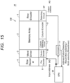
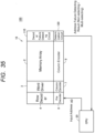
- FIG. 1 is a diagram for explaining an outline of a semiconductor device 1 according to the first embodiment.
- a semiconductor device 1 includes a memory macro 15 and a CPU20.
- CPU20 controls the memory macro 15 to acquire data stored in the memory macro 15.
- the memory macro 15 includes a memory array 2, a word driver 3, a row decoder 4, a detection circuit 5, a row encoder 6, a column selection circuit 7, a pre-decoder 8, a column encoder 9, and a column decoder 10.
- the memory array 2 includes a plurality of memory cells MC arranged in a matrix.
- the memory array 2 includes a plurality of word lines WL provided corresponding to the memory cell rows, respectively, and a plurality of bit lines BL provided corresponding to the memory cell rows, respectively.
- the word driver 3 drives one word line WL among a plurality of word lines WL provided respectively corresponding to the memory cell rows.
- a plurality of row select lines RWL are provided between the row decoder 4 and the word driver 3.
- the pre-decoder 8 decodes the input address information IAD and outputs it to the row decoder 4 and the column decoder 10 separately into the input row address information RAD and the input column address information CAD, respectively.
- the input row address information RAD of 4 bits is divided into the input row address information RAD of 7 bits and the input column address information CAD of 3 bits, and is output to the row decoder 4 and the column decoder 10, respectively.
- the row decoder 4 outputs a row selection signal to a plurality of row selection lines RWL based on the input row address information RAD.
- the word driver 3 selects the word line WL according to the low selection signal and rises to the "H" level.
- Detection circuit 5 detects faults in row decoder 4 and column decoder 10.
- the row encoder 6 is connected to a plurality of word lines WL, and encodes row address information on the basis of the rising edge of the selected word line WL.
- the column selection circuit 7 selects one of the plurality of bit lines BL.
- a plurality of column selection lines Y are provided between the column decoder 10 and the column selection circuit 7.
- the column decoder 10 outputs a column selection signal to a plurality of column selection lines Y based on the input column address information CAD.
- the column encoder 9 is connected to a plurality of column select lines Y, and encodes column address information based on the rising edge of the selected column select line Y.
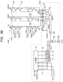
- Figure 2 is a diagram illustrating a memory array 2 and its peripheral circuits according to the first embodiment.
- the memory array 2 includes a plurality of memory cells MC arranged in a matrix, a plurality of word lines WL provided corresponding to each memory cell row, and a plurality of bit lines BL, /BL provided corresponding to each memory cell row.
- word lines WL [0] to WL [15] are provided corresponding to the memory cell rows, respectively.
- Bit lines BL[0] to BL[7] and complementary bit lines /BL[0] to /BL[7] are provided corresponding to the memory cell columns, respectively.
- the row decoder 4 outputs a row selection signal to a plurality of row selection lines RWL[0] to RWL[15] based on the input row address information RAD.
- the word driver 3 is connected to a plurality of row selection lines RWL[0] to RWL[15], and includes a driver unit for driving one word line WL among the plurality of word lines WL[0] to WL[15]. For example, when the row selection line RWL[0] is set to the "H" level, the word driver 3 selects the word line WL[0]. Specifically, the word line WL[0] is set to the "H" level. The same applies to other word lines WL.
- the column decoder 10 outputs a column selection signal to a plurality of column selection lines Y[0] to Y[7] based on the input column address information CAD.
- the column selection circuit 7 is connected to a plurality of column selection lines Y[0] to Y[7] to select one of the plurality of bit lines BL. Specifically, connecting the read circuit/write circuit 12 and the bit line BL. The read/write circuit 12 outputs a data signal read through the selected bit line BL as read data DTO at the time of data reading. The read/write circuit 12 writes the input write data DTI to the memory cell MC via the selected bit line BL at the time of data writing.
- 1-bit data reading and data writing are described in this example, the present invention is not limited to this, and it is of course possible to perform parallel reading and parallel writing of a plurality of bits (8 bits, 16 bits, etc.).
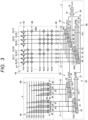
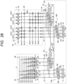
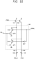
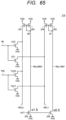
- Figure 3 is a diagram illustrating a detection circuit 5 according to the first embodiment, the circuit configuration of the row encoder 6 and the column encoder 9.
- the row encoder 6 includes a first row encoder 6A, a second row encoder 6B, a precharge circuit 6C, and a driver circuit 6D.
- the first row coder 6A includes a plurality of word lines WL[0] to WL[15], a plurality of data lines DL[0] to DL[3], and a plurality of dummy cells DMCs arranged in a predetermined first pattern in a matrix at positions where the word lines WL and the data lines DL intersect.
- the second row coder 6B includes a plurality of word lines WL[0] to WL[15], a plurality of data lines DL[4] to DL[7], and a plurality of dummy cells DMCs arranged in a predetermined second pattern in a matrix.
- the precharge circuit 6C is provided corresponding to a plurality of data lines DL[0] to DL[7] respectively, and includes a plurality of precharge transistors PT for precharging a plurality of data lines DL[0] to DL[7] to a predetermined voltage.
- the precharge transistor PT operates according to the control signal PCB, and precharges a plurality of data lines DL[0] to DL[7] to a predetermined voltage when the control signal PCB is at the "L" level.
- the driver circuit 6D includes inverters provided corresponding to the plurality of data lines DL[0] to DL[7], respectively, and inverting and outputting data of the plurality of data lines DL[0] to DL[7].
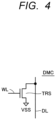
- FIG. 4 is a diagram illustrating a configuration of a dummy cell DMC according to the first embodiment.
- the dummy cell DMC includes a transistor TRS.
- the transistor TRS is connected between the fixed voltage VSS and the data line DL, and the gate is connected to the word line WL. Therefore, when the word line WL is at the "H” level, the transistor TRS is turned on, and the data line DL is set to the "L" level.
- the dummy cell DMC arranged at the position crossing the word line WL and the data line DL becomes conductive, and the data line DL is set to the "L" level.
- the plurality of dummy cells DMCs provided in the first row coder 6A are arranged in predetermined first patterns so as to encode address information for selecting any word line WL when the word line WL is selected.
- the dummy cell DMC is not arranged at a position crossing the word line WL[0] and the data lines DL[0] to DL[3].
- the data lines DL[0] to DL[3] maintain the precharged predetermined voltage level ("H" level).
- the driver circuit 6D inverts the data of the data lines DL[0] to DL[3] and outputs the inverted data ("L" level).
- the first row coder 6A when the word line WL[0] is selected, the first row coder 6A generates the first row address data RT ("0000") by the driver circuits 6D via the data lines DL[0] to DL[3]. The first row coder 6A generates the first row address data RT for selecting the word line WL via the data lines DL[0] to DL[3] in the same manner even when another word line WL is selected.
- the second row coder 6B generates second row address information RB complementary to the first row coder 6A.
- the plurality of dummy cells DMCs provided in the second row coder 6B are arranged in predetermined second patterns so as to encode address information for selecting any word line WL when the word line WL is selected.
- the dummy cell DMC is arranged at a position crossing the word line WL[0] and the data lines DL[4] to DL[7].
- the data lines DL[4] to DL[7] are set to the "L" level from the precharged predetermined voltage level.
- the driver circuit 6D inverts the data of the data line DL and outputs the inverted data.
- the driver-circuit 6D is "L” level, the data shall be "0”.
- the driver-circuit 6D is "H” level, the data shall be "1".
- the second row coder 6B when the word line WL[0] is selected, the second row coder 6B generates the second row address data RB ("1111") by the driver circuits 6D via the data lines DL[4] to DL[7]. The second row coder 6B generates the second row address data RB for selecting the word line WL via the data lines DL[4] to DL[7] in the same manner when another word line WL is selected.
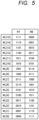
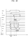
- FIG. 5 is a diagram illustrating the relationship between the selection of the word line WL and the encoded first row address information RT and the second row address information RB.
- the first row address information RT and the second row address information RB according to the selection of the word lines WL[0] to WL[15] are shown.
- the first row address information RT and the second row address information RB are shown as complementary relationships to each other.
- the column encoder 9 includes a first column encoder 9A and a second column encoder 9B.
- the first column encoder 9A includes a plurality of column select lines Y[0]-Y[7], a plurality of NOR circuitry 41,42,44,45,46,48, and a plurality of NAND circuitry 40,43,47.
- a plurality of NOR circuitry and a plurality of NAND circuitry provided in the first column encoder 9A are connected in a predetermined combination with the column select line Y so as to decode the address information for selecting the column select line Y if any column select line Y is selected.
- the NOR circuit 41 receives inputs from the column select line Y[7] and the column select line Y[6], and outputs a NOR logical operation result.
- the NOR circuit 42 receives inputs from the column select line Y[5] and the column select line Y[4], and outputs a NOR logical operation result.
- the NOR circuit 44 receives inputs from the column select line Y[7] and the column select line Y[6], and outputs a NOR logical operation result.
- the NOR circuit 45 receives inputs from the column select line Y[3] and the column select line Y[2], and outputs a NOR logical operation result.
- the NOR circuit 46 receives inputs from the column select line Y[7] and the column select line Y[5], and outputs a NOR logical operation result.
- the NOR circuit 48 receives inputs from the column select line Y[3] and the column select line Y[1], and outputs a NOR logical operation result.
- NAND circuit 40 outputs a NAND logical operation result by receiving an input from the NOR circuit 41 and 42.
- NAND circuit 43 outputs NAND logical operation result by receiving an input from the NOR circuit 44 and 45.
- NAND circuit 45 outputs NAND logical operation result by receiving an input from the NOR circuit 46 and 48.
- the NOR circuits 41, 44, and 46 connected to the column select line Y[7] output an "L" level.
- NAND circuitry 40, 43, 47 in accordance with this outputs a "H" level, respectively.
- the first column encoder 9A generates the first column address information CT ("111") when the column selection line Y[7] is selected.
- the first column encoders 9A generate first column address information CT for selecting the column selection lines Y in the same manner when the column selection lines Y are selected.
- the second column encoder 9B generates second column address information CB complementary to the first column encoder 9A.
- the second column encoder 9B includes a plurality of column select lines Y[0]-Y[7], a plurality of NOR circuitry 49,51,52,54,55,57, and a plurality of NAND circuitry 50,53,56.
- the first column encoder 9A and the second column encoder 9B may be configured using dummy cells DMCs, similarly to the first row encoder 6A and the second row encoder 6B.
- a plurality of NOR circuitry and a plurality of NAND circuitry provided in the second column encoder 9B are connected in a predetermined combination with the column select line Y so as to decode the address information for selecting the column select line Y if any column select line Y is selected.
- the NOR circuit 49 receives inputs from the column select line Y[3] and the column select line Y[2], and outputs a NOR logical operation result.
- the NOR circuit 51 receives inputs from the column select line Y[1] and the column select line Y[0], and outputs a NOR logical operation result.
- the NOR circuit 52 receives inputs from the column select line Y[5] and the column select line Y[4], and outputs a NOR logical operation result.
- the NOR circuit 54 receives inputs from the column select line Y[1] and the column select line Y[0], and outputs a NOR logical operation result.
- the NOR circuit 55 receives inputs from the column select line Y[6] and the column select line Y[4], and outputs a NOR logical operation result.
- the NOR circuit 57 receives inputs from the column select line Y[2] and the column select line Y[0], and outputs a NOR logical operation result.
- NAND circuit 50 outputs a NAND logical operation result by receiving an input from the NOR circuit 49 and 51.
- NAND circuit 53 outputs a NAND logical operation result by receiving an input from the NOR circuit 52 and 54.
- NAND circuit 56 outputs NAND logical operation result by receiving an input from the NOR circuit 55 and 57.
- NAND circuitry 50, 53, 56 maintains a "L" level.
- the second column encoders 9B generate the second column address information CB ("000") when the column selection line Y[7] is selected.
- the second column encoders 9B generate second column address information CB for selecting the column selection lines Y in the same manner when the column selection lines Y are selected.
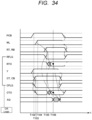
- FIG. 6 is a diagram for explaining a relationship between selection of the column selection line Y and encoded first column address information CT and second column address information CB.
- the first column address information CT and the second column address information CB according to the selection of the column selection lines Y[0] to Y[7] are shown.
- the detecting circuit 5 includes a first row judging circuit 5A, a second row judging circuit 5B, a first column judging circuit 5C, a second column judging circuit 5D, and a synthesizing circuit 5E.
- the first row determination circuit 5A includes EXOR circuitry 64-67 and NAND circuitry 70.
- the second row determination circuit 5B includes EXOR circuitry 60-63 and NOR circuitry 72.
- the first column determination circuit 5C includes EXOR circuitry 33-35 and NAND circuitry 36.
- the second column determination circuit 5D includes EXOR circuitry 30-32 and NAND circuitry 37.
- the combining circuit 5E includes a NAND circuit 74, an OR circuit 75, and a flip-flop (FF) 76.
- the first row determination circuit 5A outputs a first row determination signal RFLG based on the comparison result by comparing the first row address information RT and the second row address information RB.
- EXOR circuits 64 to 67 receive respective one-bit inputs of the first row address information RT and the second row address information RB, and outputs EXOR logical operation result RBO to NAND circuit 70.
- the first row address information RT and the second row address information RB are complementary to each other when they are normal.
- the first row determination signal RFLG ("H" level), it is determined that the first row address information RT and the second row address information RB is not complementarily related (if not normal). That is, it is determined that the row decoder 4 has an anomaly and is not normally decoded.
- a multi-selection abnormality when a plurality of word lines WL is not selected and a multi-selection abnormality when a plurality of word lines WL among a plurality of word lines WL is selected are determined.
- the second row determination circuit 5B compares the input row address information RAD with the first row address information RT, and outputs a second row determination signal RCMP based on the result of the comparison.
- EXOR circuits 60 to 63 receive input of the input row address information RAD and the first row address information RT bit by bit, respectively, and outputs EXOR logical operation result RTO to the NOR circuit 72.
- the input row address information RAD and the first row address information RT have the same relationship when they are normal.
- the second row determination signal RCMP ("L" level), it is determined that the input low address information RAD and the first low address information RT is not the same relationship (if not normal). That is, it is determined that the row decoder 4 has an anomaly and is not normally decoded.
- an erroneous selection anomaly in which an erroneous word line WL is selected among the plurality of word lines WL is determined by an abnormality in the row decoder 4.
- the first column determination circuit 5C compares the first column address information CT with the second column address information CB, and outputs a first column determination signal CFLG based on the compared result.
- EXOR circuits 33 to 35 receive one-bit inputs of the first column address information CT and the second column address information CB, respectively, and outputs EXOR logical operation result CBO to NAND circuit 36.
- the first column address information CT and the second column address information CB are complementary to each other when they are normal.
- the first column determination signal CFLG (“H" level) it is determined that the first column address information CT and the second column address information CB are not complementarily related (when they are not normal). That is, it is determined that the column decoder 10 has an anomaly and is not normally decoded.
- a non-selection anomaly in the case where no plurality of column selection lines Y are selected and a multi-selection abnormality in the case where a plurality of column selection lines Y are selected among the plurality of column selection lines Y are determined by an abnormality of the column decoder 10.
- the second column determination circuit 5D compares the input column address information CAD with the first column address information CT, and outputs a second column determination signal CCMP based on the result of the comparison.
- EXOR circuits 30 to 32 receive inputs of the input column address information CAD and the first column address information CT, one bit at a time, and outputs EXOR logical operation result CTO to the NOR circuit 37.
- the input column address information CAD and the first column address information CT have the same relationship when they are normal.
- the second column determination signal CCMP ("L" level) it is determined that the input column address information CAD and the first column address information CT do not have the same relationship (when they are not normal). That is, it is determined that the column decoder 10 has an anomaly and is not normally decoded.
- an erroneous selection anomaly in which an erroneous column selection line Y is selected among the plurality of column selection lines Y is determined by an abnormality in the column decoder 10.
- NAND circuit 74 outputs NAND logical operation result to the OR circuit 75 in response to an input of the second row determination signal RCMP and the second column determination signal RCMP.
- the OR circuit 75 receives the first row determination signal RFLG, the first column determination signal CFLG, and the output of NAND circuit 74 and outputs the OR logical operation result to the flip-flop 76.
- OR circuit 75 includes a first low determination signal RFLG ("L” level), a second low determination signal RCMP ("H” level), the first column determination signal CFLG ("L” level), the second column determination signal CCMP ("H” level) if the stores the "L” level to the flip-flop 76.
- the OR circuit 75 stores the first low determination signal RFLG ("H” level), the second low determination signal RCMP ("L” level), the first column determination signal CFLG ("H” level), the second column determination signal CCMP ("L” level) in the flip-flop 76 if any of the states.
- the flip-flop 76 outputs abnormal signals FLAG based on the stored data.
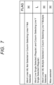
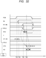
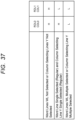
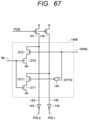
- FIG. 7 is a diagram for explaining an abnormality of the row decoder 4 and the column decoder 10 according to the first embodiment.
- the abnormality signal FLAG H level
- RFLG H level
- the abnormality signal FLAG H level
- RCMP L level
- the abnormality signal FLAG H level
- CFLG H level
- the abnormality signal FLAG H level
- CCMP L level
- the error signal FLAG is set to "L" level.
- the detecting circuit 5 outputs the abnormal signal FLAG to CPU20.
- the detector 5 outputs abnormal signals FLAG at the time of data reading and data writing. Therefore, according to the configuration of the first embodiment, it is possible to detect the failure of the address decoder (the row decoder 4 and the column decoder 10) at an early stage in a simple method.
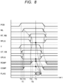
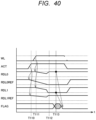
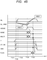
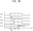
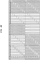
- FIG. 8 is a first timing chart illustrating the operation of the semiconductor device 1 according to the first embodiment.
- the control signal PCB is set to a "H" level.
- the precharge operation for the data lines DL[0] to DL[7] of the precharge circuit 6C is completed.
- the column decoder 10 selects one of the plurality of column selection lines Y based on the input column address information CAD.
- the first and second column encoders 9A,9B generate first column address information CT and second column address information CB, respectively.
- the first column address information CT and the second column address information CB are generated as complementary relationships with each other.
- the first column relationship circuit 5C compares the first column address information CT and the second column address information CB and outputs the first column determination signal CFLG ("L" level) because the first column determination circuit 5C is complementary to each other.
- the second column determination circuit 5D outputs the second column determination signal CCMP ("H" level) because the input column address information CAD and the first column address information CT are compared and matched.
- the row decoder 4 selects one of the plurality of word lines WL based on the input row address information RAD.
- the first and second row coders 6A,6B generate first row address information RT and second row address information RB, respectively.
- the first row address information RT and the second row address information RB are generated as complementary relationships with each other.
- the first row determination circuit 5A outputs a first row determination signal RFLG ("L" level) because it is complementarily related to each other by comparing the first row address information RT and the second row address information RB.
- the second row determination circuit 5B outputs a second row determination signal RCMP for matches by comparing the input low address information RAD and the first low address information RT ("H" level).
- the detection circuit 5 At time T5, the detection circuit 5, the first row test signal RFLG ("L” level), a second low determination signal RCMP ("H” level), the first column determination signal CFLG ("L” level), and outputs an abnormal signal FLAG ("L” level) based on the second column determination signal CCMP ("H” level).
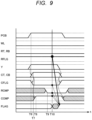
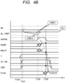
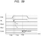
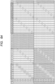
- Figure 9 is a timing chart diagram for explaining the operation of the semiconductor device 1 according to the first embodiment (Part 2).
- the control signal PCB is set to a "H" level.
- the precharge operation for the data lines DL[0] to DL[7] of the precharge circuit 6C is completed.
- the column decoder 10 selects one of the plurality of column selection lines Y based on the input column address information CAD.
- the first and second column encoders 9A,9B generate first column address information CT and second column address information CB, respectively.
- the first column address information CT and the second column address information CB are generated as complementary relationships with each other.
- the first column determination circuit 5C compares the first column address information CT with the second column address information CB, and outputs the first column determination signal CFLG ("L" level) because the first column determination circuit 5C has a complementary relation with the second column address information CB.
- the second column determination circuit 5D outputs the second column determination signal CCMP ("H" level) because the input column address information CAD and the first column address information CT are compared and matched.
- the row decoder 4 does not select one of the plurality of word lines WL based on the input row address information RAD due to an error.
- the first and second row coders 6A,6B generate the first row address information RT and the second row address information RB, respectively, but in the present embodiment, the first row address information RT and the second row address information RB are not generated as mutually complementary relationships.
- the first row determination circuits 5A compare the first row address information RT and the second row address information RB and maintain the first row determination signals RFLG ("H" levels) because they are not complementary to each other.
- the second row determination circuit 5B outputs a second row determination signal RCMP ("L" level) because it does not match by comparing the input row address information RAD and the first row address information RT.
- the detection circuit 5 the first row determination signal RFLG ("H” level), a second low determination signal RCMP ("L” level), the first column determination signal CFLG ("L” level), and outputs an abnormal signal FLAG ("H” level) based on the second column determination signal CCMP ("H” level).
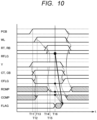
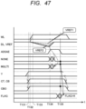
- Figure 10 is a timing chart diagram for explaining the operation of the semiconductor device 1 according to the first embodiment (its 3).
- the control signal PCB is set to a "H" level.
- the precharge operation for the data lines DL[0] to DL[7] of the precharge circuit 6C is completed.
- the column decoder 10 selects one of the plurality of column selection lines Y based on the input column address information CAD.
- the first and second column encoders 9A,9B generate first column address information CT and second column address information CB, respectively.
- the first column address information CT and the second column address information CB are generated as complementary relationships with each other.
- the first column relationship circuit 5C compares the first column address information CT and the second column address information CB and outputs the first column determination signal CFLG ("L" level) because the first column determination circuit 5C is complementary to each other.
- the second column determination circuit 5D outputs the second column determination signal CCMP ("H" level) because the input column address information CAD and the first column address information CT are compared and matched.
- the row decoder 4 selects a plurality of word lines WL among the plurality of word lines WL due to an abnormality based on the input row address information RAD.
- the first and second row coders 6A,6B generate the first row address information RT and the second row address information RB, respectively, but in the present embodiment, the first row address information RT and the second row address information RB are not generated as mutually complementary relationships.
- the first row determination circuits 5A compare the first row address information RT and the second row address information RB and maintain the first row determination signals RFLG ("H" levels) because they are not complementary to each other.
- the second row determination circuit 5B compares the input row address information RAD with the first row address information RT, and outputs the second row determination signal RCMP ("L" level) because the input row address information RAD does not coincide with the first row address information RT.
- the case of outputting the second row determination signal RCMP ("L" level) will be described, but depending on the condition, the case of outputting the second row determination signal RCMP ("H" level) coincident with the case of comparing the inputted row address information RAD and the first row address information RT may be considered.
- the detection circuit 5 At time T16, the detection circuit 5, the first row determination signal RFLG ("H” level), a second low determination signal RCMP ("L” level), the first column determination signal CFLG ("L” level), and outputs an abnormal signal FLAG ("H” level) based on the second column determination signal CCMP ("H" level).
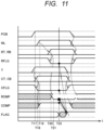
- Figure 11 is a timing chart diagram for explaining the operation of the semiconductor device 1 according to the first embodiment (its 4).
- the control signal PCB is set to a "H" level.
- the precharge operation for the data lines DL[0] to DL[7] of the precharge circuit 6C is completed.
- the column decoder 10 selects one of the plurality of column selection lines Y based on the input column address information CAD.
- the first and second column encoders 9A,9B generate first column address information CT and second column address information CB, respectively.
- the first column address information CT and the second column address information CB are generated as complementary relationships with each other.
- the first column relationship circuit 5C compares the first column address information CT and the second column address information CB and outputs the first column determination signal CFLG ("L" level) because the first column determination circuit 5C is complementary to each other.
- the second column determination circuit 5D outputs the second column determination signal CCMP ("H" level) because the input column address information CAD and the first column address information CT are compared and matched.
- the row decoder 4 selects the wrong word line WL among the plurality of word lines WL due to an error based on the input row address information RAD.
- the first and second row coder 6A,6B generate the first row address information RT and the second row address information RB, respectively, but in this example, the first row address information RT and the second row address information RB are generated as complementary relationships to each other according to the wrong word line WL.
- the first row determination circuit 5A outputs a first row determination signal RFLG ("L" level) because it is complementary to each other by comparing the first row address information RT and the second row address information RB.
- the second row determination circuit 5B compares the input row address information RAD with the first row address information RT, and outputs the second row determination signal RCMP ("L" level) because the input row address information RAD does not coincide with the first row address information RT.
- the detection circuit 5 At time T22, the detection circuit 5, the first row test signal RFLG ("L” level), a second low determination signal RCMP ("L” level), the first column determination signal CFLG ("L” level), and outputs an abnormal signal FLAG ("H” level) based on the second column determination signal CCMP ("H" level).
- FIG. 12 is a timing chart (5) illustrating the operation of the semiconductor device 1 according to the first embodiment.
- the control signal PCB is set to a "H" level.
- the precharge operation for the data lines DL[0] to DL[7] of the precharge circuit 6C is completed.
- the column decoder 10 does not select one of the plurality of column selection lines Y based on the input column address information CAD.
- the first and second column encoders 9A,9B generate the first column address information CT and the second column address information CB, respectively, but in the present embodiment, the first column address information CT and the second column address information CB are not generated as mutually complementary relationships.
- the first column determination circuit 5C compares the first column address information CT with the second column address information CB, and maintains the first column determination signal CFLG ("H" level) because the first column determination circuit does not have a complementary relation with the second column address information CB.
- the second column determination circuit 5D outputs the second column determination signal CCMP ("L" level) because the input column address information CAD and the first column address information CT are compared and do not match.
- the row decoder 4 selects one of the plurality of word lines WL based on the input row address information RAD.
- the first and second row coders 6A,6B generate first row address information RT and second row address information RB, respectively.
- the first row address information RT and the second row address information RB are generated as complementary relationships with each other.
- the first row determination circuit 5A outputs a first row determination signal RFLG ("L" level) because it is complementarily related to each other by comparing the first row address information RT and the second row address information RB.
- the second row determination circuit 5B outputs a second row determination signal RCMP for matches by comparing the input low address information RAD and the first low address information RT ("H" level).
- the detection circuit 5 the first low test signal RFLG ("L” level), a second low determination signal RCMP ("H” level), the first column determination signal CFLG ("H” level), and outputs an abnormal signal FLAG ("H” level) based on the second column determination signal CCMP ("L” level).
- Figure 13 is a timing chart diagram for explaining the operation of the semiconductor device 1 according to the first embodiment (Part 6).
- the control signal PCB is set to a "H" level.
- the precharge operation for the data lines DL[0] to DL[7] of the precharge circuit 6C is completed.
- the column decoder 10 selects a plurality of column selection lines Y based on the input column address information CAD.
- the first and second column encoders 9A,9B generate the first column address information CT and the second column address information CB, respectively, but in this embodiment, the first column address information CT and the second column address information CB are not generated as complementary relationships with each other.
- the first column determination circuit 5C compares the first column address information CT with the second column address information CB, and maintains the first column determination signal CFLG ("H" level) because the first column determination circuit does not have a complementary relation with the second column address information CB.
- the second column determination circuit 5D outputs the second column determination signal CCMP ("L" level) because the input column address information CAD and the first column address information CT are compared and do not match.
- the row decoder 4 selects one of the plurality of word lines WL based on the input row address information RAD.
- the first and second row coders 6A,6B generate first row address information RT and second row address information RB, respectively.
- the first row address information RT and the second row address information RB are generated as complementary relationships with each other.
- the first row determination circuit 5A outputs a first row determination signal RFLG ("L" level) because it is complementarily related to each other by comparing the first row address information RT and the second row address information RB.
- the second row determination circuit 5B outputs a second row determination signal RCMP for matches by comparing the input low address information RAD and the first low address information RT ("H" level).
- the detection circuit 5 the first low test signal RFLG ("L” level), a second low determination signal RCMP ("H” level), the first column determination signal CFLG ("H” level), and outputs an abnormal signal FLAG ("H” level) based on the second column determination signal CCMP ("L” level).
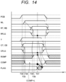
- Figure 14 is a timing chart diagram for explaining the operation of the semiconductor device 1 according to the first embodiment (Part 7).
- the control signal PCB is set to a "H" level.
- the precharge operation for the data lines DL[0] to DL[7] of the precharge circuit 6C is completed.
- the column decoder 10 selects the incorrect column selection line Y among the plurality of column selection lines Y based on the input column address information CAD.
- the first and second column encoders 9A,9B generate the first column address information CT and the second column address information CB, respectively, but in this embodiment, the first column address information CT and the second column address information CB are generated in complementary relation to each other in accordance with the erroneous column selection line Y.
- the first column determination circuit 5C compares the first column address information CT with the second column address information CB, and outputs the first column determination signal CFLG ("L" level) because the first column determination circuit is complementary to the second column address information CB.
- the second column determination circuit 5D outputs the second column determination signal CCMP ("L" level) because the input column address information CAD and the first column address information CT are compared and do not match.
- the row decoder 4 selects one of the plurality of word lines WL based on the input row address information RAD.
- the first and second row coders 6A,6B generate first row address information RT and second row address information RB, respectively.
- the first row address information RT and the second row address information RB are generated as complementary relationships with each other.
- the first row determination circuit 5A outputs a first row determination signal RFLG ("L" level) because it is complementarily related to each other by comparing the first row address information RT and the second row address information RB.
- the second row determination circuit 5B outputs a second row determination signal RCMP for matches by comparing the input low address information RAD and the first low address information RT ("H" level).
- the detection circuit 5 the first low determination signal RFLG ("L” level), a second low determination signal RCMP ("H” level), the first column determination signal CFLG ("H” level), and outputs an abnormal signal FLAG ("H” level) based on the second column determination signal CCMP ("L" level).
- FIG. 15 is a diagram for explaining an outline of the semiconductor device 1# according to the second embodiment.
- the semiconductor device 1# includes a memory macro 15#, a CPU20, and a comparator 11.
- CPU20 controls the memory macro 15# to acquire the data stored in the memory macro 15#.
- the memory macro 15# differs from the memory macro 15 in that the detection circuit 5 is replaced with a detection circuit 5P. Since the other configurations are the same, detailed description thereof will not be repeated.
- the detecting circuit 5P outputs the first row address information RT and the second row address information RB output from the row encoder 6 and the output address information AQ based on the first column address information CT and the second column address information CB output from the column encoder 9.
- the output address information AQ includes an output row address information ORAD and an output column address information OCAD.
- the comparator circuit 11 compares the output address information AQ output from the detector circuit 5P with the input address information IAD, and outputs the comparison result to CPU20.
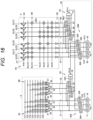
- Fig. 16 is a diagram illustrating a circuit configuration of a detection circuit 5P, a row encoder 6, and a column encoder 9 according to the second exemplary embodiment.
- the detection circuit 5P includes a first row determination circuit 5A, a second row determination circuit OOC#, a first column determination circuit 5C, and a second column determination circuit OOA#.
- the first row determination circuit 5A includes EXOR circuitry 64-67 and NAND circuitry 70.
- the second row determination circuit 5B# includes EXOR circuitry 60# to 63# and flip-flops (FFFs) 80 to 83.
- the first column determination circuit 5C includes EXOR circuitry 33-35 and NAND circuitry 36.
- the second column determination circuitry 5D# includes EXOR circuitry 30# to 32# and flip-flops (FFs) 77 to 79.
- the first row determination circuit 5A outputs a first row determination signal RFLG based on the comparison result by comparing the first row address information RT and the second row address information RB.
- the first row determination signal RFLG (“H" level)
- the first row address information RT and the second row address information RB is not complementarily relationship (if not normal). That is, it is determined that the row decoder 4 has an anomaly and is not normally decoded.
- a multi-selection abnormality when a plurality of word lines WL is not selected and a multi-selection abnormality when a plurality of word lines WL among a plurality of word lines WL is selected are determined.
- the second row determination circuit 5B# generates an output row address information ORAD based on the first row address information RT and the first column determination signal CFLG.
- EXOR circuits 60# to 63# receive 1-bit of the first row address information RT and the first column determination signal CFLG, respectively, and output EXOR logical operation result RTO to the flip-flops 80 to 83, respectively.
- the first column determination signal CFLG is set to "L" level.
- the first column determination signals CFLG are set to "H" levels.
- EXOR circuitry 60# to 63# receive the input of the first low address information RT and the first column determination signal CFLG ("L" level) and output EXOR logical operation result RTO to the flip-flops 80 to 83, respectively.
- the first row address information RT is set to the first column determination signal CFLG ("L" level), the first row address information RT is directly outputted to the flip-flops 80 to 83 as EXOR logical operation result RTO.
- the first low address information RT is latched by the flip-flops 80 to 83 and is output to the comparator circuit 11 as the output low address information ORAD.
- EXOR circuitry 60# to 63# receive the input of the first low address information RT and the first column determination signal CFLG ("H" level) and output EXOR logical operation result RTO to the flip-flops 80 to 83, respectively.
- the first row address information RT is set to the first column determination signal CFLG ("H" level)
- the first row address information RT is inverted. For example, when the first row address information RT is "1111", EXOR logical operation result RTO changes to "0000". That is, the first row address information RT is changed to inverted address information in accordance with the first column determination signal CFLG ("H" level).
- the inverted first row address information RT is latched by the flip-flops 80 to 83 and is output to the comparator circuit 11 as the output row address information ORAD.
- the comparator 11 since the output row address information ORAD is changed, the output address information AQ and the input address information IAD are compared with each other, and the comparison results do not coincide with each other. That is, the non-coincidence test signals are outputted to CPU20.
- the first column determination circuit 5C compares the first column address information CT with the second column address information CB, and outputs a first column determination signal CFLG based on the compared result.
- the first column determination signal CFLG (“H" level) determines that the first column address information CT and the second column address information CB are not complementarily related (when they are not normal). That is, it is determined that the column decoder 10 has an anomaly and is not normally decoded.
- a non-selection anomaly in the case where no plurality of column selection lines Y are selected and a multi-selection abnormality in the case where a plurality of column selection lines Y are selected among the plurality of column selection lines Y are determined by an abnormality of the column decoder 10.
- the second column determination circuit OOC# generates the output column address information OCAD based on the second column address information CB and the first row determination signal RFLG.
- EXOR circuits 30# to 32# output EXOR logical operation result CTOs to the flip-flops 77 to 79 by receiving the input of the first bit of the first column address information CT and the first row determination signal RFLG, respectively.
- the first row determination signals RFLG are set to "L” levels.
- the first row determination signal RFLG is set to the "H" level.
- EXOR circuits 30# to 32# receive the input of the first column address information CT and the first row determination signal RFLG ("L" level) and output EXOR logical operation result CTO to the flip-flops 77 to 79, respectively.
- the first column address information CT is output as it is to the flip-flops 77 to 79 as EXOR logical operation result CTO, respectively.
- the first column address information CT is latched by flip-flops 77 to 79 and output to the comparator circuit 11 as output column address information OCAD.
- EXOR circuits 30# to 32# receive the input of the first column address information CT and the first row determination signal RFLG ("H" level) and output EXOR logical operation result CTO to the flip-flops 77 to 79, respectively.
- the data of the first column address information CT is inverted. For example, when the first column address information CT is "111", EXOR logical operation result CTO changes to "000". That is, the first column address information CT is changed to inverted address information in accordance with the first row determination signal RFLG ("H" level) .
- the inverted first column address information CT is latched by flip-flops 77 to 79 and output as output column address information OCAD to the comparator circuit 11.
- the comparator 11 since the output column address information OCAD is changed, the output address information AQ and the input address information IAD are compared with each other, and the comparison results do not coincide with each other. That is, the non-coincidence test signals are outputted to CPU20.
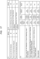
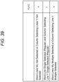
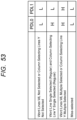
- FIG. 17 is a diagram for explaining an anomaly of the row decoder 4 and the column decoder 10 according to the second embodiment.
- the first row determination signals RFLG (“H" levels) are outputted.
- the first column determination signals CFLG (“H" levels) are outputted.
- the comparison circuit 11 outputs a determination signal (Fail) that does not coincide with the comparison result when the input address information IAD and the output address information AQ are compared with each other to CPU20.
- the output address information AQ output from the detecting circuits 5P includes correct row address information and column address information.
- the comparator 11 outputs a determination signal Pass that matches the comparison result to CPU20.
- the comparison circuit 11 outputs a determination signal (Fail) that does not coincide with the comparison result when the input address information IAD and the output address information AQ are compared with each other to CPU20.
- the output address information AQ output from the detecting circuits 5P includes erroneous row address information or column address information.
- the comparison circuit 11 outputs a determination signal (Fail) that does not coincide with the comparison result when the input address information IAD and the output address information AQ are compared with each other to CPU20.
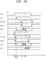
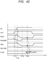
- FIG. 18 is a timing chart illustrating the operation of the semiconductor device 1# according to the second embodiment.
- the control signal PCB is set to a "H" level.
- the precharge operation for the data lines DL[0] to DL[7] of the precharge circuit 6C is completed.
- the column decoder 10 selects one of the plurality of column selection lines Y based on the input column address information CAD.
- the first and second column encoders 9A,9B generate first column address information CT and second column address information CB, respectively.
- the first column address information CT and the second column address information CB are generated as complementary relationships with each other.
- the first column relationship circuit 5C compares the first column address information CT and the second column address information CB and outputs the first column determination signal CFLG ("L" level) because the first column determination circuit 5C is complementary to each other.
- the row decoder 4 selects one of the plurality of word lines WL based on the input row address information RAD.
- the first and second row coders 6A, 6B generate first row address information RT and second row address information RB, respectively.
- the first row address information RT and the second row address information RB are generated as complementary relationships with each other.
- the first row determination circuit 5A outputs a first row determination signal RFLG ("L" level) because it is complementarily related to each other by comparing the first row address information RT and the second row address information RB.
- the first column address information CT is output as it is to the flip-flops 77 to 79 as EXOR logical operation result CTO, respectively. Since the first column determination signal CFLG ("L" level) is set, the first row address information RT is directly outputted to the flip-flops 80 to 83 as EXOR logical operation result RTO.
- the detector 5P outputs output address information AQ including correct row address information and column address information.
- the comparator 11 When the input address information IAD and the output address information AQ are compared with each other when the input address information IAD is correct address information, the comparator 11 outputs a coincidence determination signal Pass to CPU20.
- Figure 19 is a timing chart diagram for explaining the operation of the semiconductor device 1# according to the second embodiment (Part 2).
- the control signal PCB is set to a "H" level.
- the precharge operation for the data lines DL[0] to DL[7] of the precharge circuit 6C is completed.
- the column decoder 10 selects one of the plurality of column selection lines Y based on the input column address information CAD.
- the first and second column encoders 9A,9B generate first column address information CT and second column address information CB, respectively.
- the first column address information CT and the second column address information CB are generated as complementary relationships with each other.
- the first column determination circuit 5C compares the first column address information CT with the second column address information CB, and outputs the first column determination signal CFLG ("L" level) because the first column determination circuit 5C has a complementary relation with the second column address information CB.
- the row decoder 4 does not select one of the plurality of word lines WL based on the input row address information RAD due to an error.
- the first and second row coders 6A,6B generate the first row address information RT and the second row address information RB, respectively, but in the present embodiment, the first row address information RT and the second row address information RB are not generated as mutually complementary relationships.
- the first column address information CT is inverted and is output as EXOR logical operation result CTO to the flip-flops 77 to 79, respectively. Since the word line WL is not selected, the first row address information RT ("1111") is directly outputted to the flip-flops 80 to 83 as EXOR logical operation result RTO.
- the detector 5P outputs output address information AQ including erroneous row address information and inverted column address information.
- the comparator 11 When the input address information IAD and the output address information AQ are compared with each other in the case where the input address information IAD is correct address information, the comparator 11 outputs a mismatch determination signal (Fail) to CPU20.
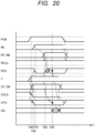
- Figure 20 is a timing chart diagram for explaining the operation of the semiconductor device 1# according to the second embodiment (Part 3).
- the control signal PCB is set to a "H" level.
- the precharge operation for the data lines DL[0] to DL[7] of the precharge circuit 6C is completed.
- the column decoder 10 selects one of the plurality of column selection lines Y based on the input column address information CAD.
- the first and second column encoders 9A,9B generate first column address information CT and second column address information CB, respectively.
- the first column address information CT and the second column address information CB are generated as complementary relationships with each other.
- the first column relationship circuit 5C compares the first column address information CT and the second column address information CB and outputs the first column determination signal CFLG ("L" level) because the first column determination circuit 5C is complementary to each other.
- the row decoder 4 selects a plurality of word lines WL among the plurality of word lines WL due to an error based on the input row address information RAD.
- the first and second row coders 6A,6B generate the first row address information RT and the second row address information RB, respectively, but in the present embodiment, the first row address information RT and the second row address information RB are not generated as mutually complementary relationships.
- the first row determination circuits 5A compare the first row address information RT and the second row address information RB and maintain the first row determination signals RFLG ("H" levels) because they are not complementary to each other.
- the first column address information CT is inverted and is output as EXOR logical operation result CTO to the flip-flops 77 to 79, respectively. Since a plurality of word lines WL are selected, the first row address information RT (unknown) is outputted to the flip-flops 80 to 83 as EXOR logical operation result RTO.
- the detector 5P outputs output address information AQ including erroneous row address information and inverted column address information.
- the comparator 11 When the input address information IAD and the output address information AQ are compared with each other in the case where the input address information IAD is correct address information, the comparator 11 outputs a mismatch determination signal (Fail) to CPU20.
- Figure 21 is a timing chart diagram for explaining the operation of the semiconductor device 1# according to the second embodiment (its 4).
- the control signal PCB is set to a "H" level.
- the precharge operation for the data lines DL[0] to DL[7] of the precharge circuit 6C is completed.
- the column decoder 10 selects one of the plurality of column selection lines Y based on the input column address information CAD.
- the first and second column encoders 9A,9B generate first column address information CT and second column address information CB, respectively.
- the first column address information CT and the second column address information CB are generated as complementary relationships with each other.
- the first column relationship circuit 5C compares the first column address information CT and the second column address information CB and outputs the first column determination signal CFLG ("L" level) because the first column determination circuit 5C is complementary to each other.
- the row decoder 4 selects the wrong word line WL among the plurality of word lines WL due to an error based on the input row address information RAD.
- the first row determination circuit 5A outputs a first row determination signal RFLG ("L" level) because it is complementary to each other by comparing the first row address information RT and the second row address information RB.
- the first column address information CT is output as it is to the flip-flops 77 to 79 as EXOR logical operation result CTO, respectively. Since the first column determination signal CFLG ("L" level) is set, the first row address information RT is directly outputted to the flip-flops 80 to 83 as EXOR logical operation result RTO.
- the detector 5P outputs output address information AQ including erroneous row address information and column address information.
- the comparator 11 When the input address information IAD and the output address information AQ are compared with each other in the case where the input address information IAD is correct address information, the comparator 11 outputs a mismatch determination signal (Fail) to CPU20.
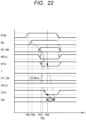
- FIG. 22 is a timing chart (5) for explaining the operation of the semiconductor device 1# according to the second embodiment.
- the control signal PCB is set to a "H" level.
- the precharge operation for the data lines DL[0] to DL[7] of the precharge circuit 6C is completed.
- the column decoder 10 does not select one of the plurality of column selection lines Y based on the input column address information CAD.
- the first and second column encoders 9A,9B generate the first column address information CT and the second column address information CB, respectively, but in the present embodiment, the first column address information CT and the second column address information CB are not generated as mutually complementary relationships.
- the first column determination circuit 5C compares the first column address information CT with the second column address information CB, and maintains the first column determination signal CFLG ("H" level) because the first column determination circuit does not have a complementary relation with the second column address information CB.
- the row decoder 4 selects one of the plurality of word lines WL based on the input row address information RAD.
- the first and second row coders 6A, 6B generate first row address information RT and second row address information RB, respectively.
- the first row address information RT and the second row address information RB are generated as complementary relationships with each other.
- the first row determination circuit 5A outputs a first row determination signal RFLG ("L" level) because it is complementarily related to each other by comparing the first row address information RT and the second row address information RB.
- the first column address information CT is output as it is to the flip-flops 77 to 79 as EXOR logical operation result CTO, respectively. Since the first column determination signal CFLG is set to the "H" level, the first row address information RT is inverted and outputted to the flip-flops 80 to 83 as EXOR logical operation result RTO.
- the detector 5P outputs output address information AQ including inverted row address information and erroneous column address information.
- the comparator 11 When the input address information IAD and the output address information AQ are compared with each other in the case where the input address information IAD is correct address information, the comparator 11 outputs a mismatch determination signal (Fail) to CPU20.
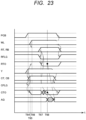
- Figure 23 is a timing chart diagram for explaining the operation of the semiconductor device 1# according to the second embodiment (Part 6).
- the control signal PCB is set to a "H" level.
- the precharge operation for the data lines DL[0] to DL[7] of the precharge circuit 6C is completed.
- the column decoder 10 selects one of the plurality of column selection lines Y based on the input column address information CAD.
- the first and second column encoders 9A,9B generate the first column address information CT and the second column address information CB, respectively, but in this embodiment, the first column address information CT and the second column address information CB are not generated as complementary relationships with each other.
- the first column determination circuit 5C compares the first column address information CT with the second column address information CB, and maintains the first column determination signal CFLG ("H" level) because the first column determination circuit does not have a complementary relation with the second column address information CB.
- the row decoder 4 selects one of the plurality of word lines WL based on the input row address information RAD.
- the first and second row coders 6A, 6B generate first row address information RT and second row address information RB, respectively.
- the first row address information RT and the second row address information RB are generated as complementary relationships with each other.
- the first row determination circuit 5A outputs a first row determination signal RFLG ("L" level) because it is complementarily related to each other by comparing the first row address information RT and the second row address information RB.
- the first column address information CT is output as it is to the flip-flops 77 to 79 as EXOR logical operation result CTO, respectively. Since the first column determination signal CFLG is set to the "H" level, the first row address information RT is inverted and outputted to the flip-flops 80 to 83 as EXOR logical operation result RTO.
- the detector 5P outputs output address information AQ including inverted row address information and erroneous column address information.
- the comparator 11 When the input address information IAD and the output address information AQ are compared with each other in the case where the input address information IAD is correct address information, the comparator 11 outputs a mismatch determination signal (Fail) to CPU20.
- FIG. 24 is a seventh timing chart illustrating the operation of the semiconductor device 1# according to the second embodiment.
- the control signal PCB is set to a "H" level.
- the precharge operation for the data lines DL[0] to DL[7] of the precharge circuit 6C is completed.
- the column decoder 10 selects an incorrect column selection line Y among the plurality of column selection lines Y based on the input column address information CAD.
- the first and second column encoders 9A,9B generate the first column address information CT and the second column address information CB, respectively, but in this embodiment, the first column address information CT and the second column address information CB are generated in complementary relation to each other in accordance with the erroneous column selection line Y.
- the first column determination circuit 5C compares the first column address information CT with the second column address information CB, and outputs the first column determination signal CFLG ("L" level) because the first column determination circuit is complementary to the second column address information CB.
- the row decoder 4 selects one of the plurality of word lines WL based on the input row address information RAD.
- the first and second row coders 6A,6B generate first row address information RT and second row address information RB, respectively.
- the first row address information RT and the second row address information RB are generated as complementary relationships with each other.
- the first row determination circuit 5A outputs a first row determination signal RFLG ("L" level) because it is complementarily related to each other by comparing the first row address information RT and the second row address information RB.
- the first column address information CT is output as it is to the flip-flops 77 to 79 as EXOR logical operation result CTO, respectively.
- the first column determination signal CFLG H
- the first row address information RT is directly outputted as EXOR logical operation result RTO to the flip-flops 80 to 83.
- the detector 5P outputs output address information AQ including row address information and erroneous column address information.
- the comparator 11 When the input address information IAD and the output address information AQ are compared with each other in the case where the input address information IAD is correct address information, the comparator 11 outputs a mismatch determination signal (Fail) to CPU20.
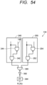
- FIG. 25 is a diagram for explaining an outline of the semiconductor device 1#A according to the third embodiment.
- the semiconductor device 1#A includes a memory macro 15#A, a CPU20, and a comparator 11.
- CPU20 controls the memory macro 15#A to acquire the data stored in the memory macro 15#A.
- the memory macro 15#A differs from the memory macro 15 in that the detection circuit 5 is replaced with a detection circuit 5Q. Since the other configurations are the same, detailed description thereof will not be repeated.
- the detecting circuit 5Q outputs the first row address information RT and the second row address information RB output from the row encoder 6 and the output address information AQ based on the first column address information CT and the second column address information CB output from the column encoder 9.
- the output address information AQ includes an output row address information ORAD and an output column address information OCAD.
- the comparator circuit 11 compares the output address information AQ output from the detector circuit 5Q with the input address information IAD, and outputs the comparison result to CPU20.
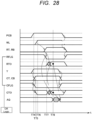
- Fig. 26 is a diagram illustrating a circuit configuration of a detection circuit 5Q, a row encoder 6, and a column encoder 9 according to the third embodiment.
- the detection circuit 5Q includes a first row determination circuit 5A, a second row determination circuit 5B#, a first column determination circuit 5C, and a second column determination circuit 5D#.
- the first row determination circuit 5A includes EXOR circuitry 64-67 and NAND circuitry 70.
- the second row determination circuit 5B# includes EXOR circuitry 60# to 63# and flip-flops (FFFs) 80 to 83.
- the first column determination circuit 5C includes EXOR circuitry 33-35 and NAND circuitry 36.
- the second column determination circuitry 5D# includes EXOR circuitry 30# to 32# and flip-flops (FFs) 77 to 79.
- the first row determination circuit 5A outputs a first row determination signal RFLG based on the comparison result by comparing the first row address information RT and the second row address information RB.
- the first column determination circuit 5C compares the first column address information CT with the second column address information CB, and outputs a first column determination signal CFLG based on the compared result.
- OR circuit 84 outputs the OR logic operation result XFLG of the first row determination signal RFLG and the first column determination signal CFLG to the second row determination circuit 5B# and the second column determination circuit 5D#, respectively.
- the second row determination circuit OOC# generates the output row address information ORAD based on the first row address information RT and the OR-logical operation result XFLG.
- the second column determination circuit OOC# generates the output column address information OCAD based on the second column address information CB and the OR-logical operation result XFLG.
- the second row determination circuit OOB# stores the first row address information RT as EXOR logical operation result RTO in the flip-flops 80 to 83, respectively.
- the second column determination circuit OOB# stores the first column address information CT as EXOR logical operation result CTO in the flip-flops 77 to 79, respectively.
- the second row determination circuit OOB# inverts the first row address information RT and stores the inverted first row address information RT in the flip-flops 80 to 83 as EXOR logical operation result RTO.
- the second column determination circuit 5D# inverts the first column address information CT and stores it as EXOR logic operation result CTO in the flip-flops 77 to 79, respectively.
- the first row determination signal RFLG when there is an anomaly in the row decoder 4 or the column decoder 10, the first row determination signal RFLG, the OR logical operation result XFLG for one of the first column determination signal CFLG becomes H level is set to H level.
- both the first row address information RT and the second column address information CT are inverted and stored in the flip-flop.
- the comparison circuit 11 outputs a mismatch determination signal (Fail) to CPU20.
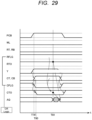
- FIG. 27 is a diagram for explaining an anomaly of the row decoder 4 and the column decoder 10 according to the third embodiment.
- the comparison circuit 11 outputs a determination signal (Fail) that does not coincide with the comparison result when the input address information IAD and the output address information AQ are compared with each other to CPU20.
- the output address information AQ output from the detecting circuits 5Q includes correct row address information and column address information.
- the comparator 11 outputs a determination signal Pass that matches the comparison result to CPU20.
- the comparison circuit 11 outputs a determination signal (Fail) that does not coincide with the comparison result when the input address information IAD and the output address information AQ are compared with each other to CPU20.
- the output address information AQ output from the detecting circuits 5Q includes erroneous row address information or column address information.
- the comparison circuit 11 outputs a determination signal (Fail) that does not coincide with the comparison result when the input address information IAD and the output address information AQ are compared with each other to CPU20.
- FIG. 28 is a first timing chart illustrating the operation of the semiconductor device 1#A according to the third embodiment.
- the control signal PCB is set to a "H" level.
- the precharge operation for the data lines DL[0] to DL[7] of the precharge circuit 6C is completed.
- the column decoder 10 selects one of the plurality of column selection lines Y based on the input column address information CAD.
- the first and second column encoders 9A,9B generate the first column address information CT and the second column address information CB, respectively.
- the first column address information CT and the second column address information CB are generated as complementary relationships with each other.
- the first column relationship circuit 5C compares the first column address information CT and the second column address information CB and outputs the first column determination signal CFLG ("L" level) because the first column determination circuit 5C is complementary to each other.
- the row decoder 4 selects one of the plurality of word lines WL based on the input row address information RAD.
- the first and second row coders 6A,6B generate first row address information RT and second row address information RB, respectively.
- the first row address information RT and the second row address information RB are generated as complementary relationships with each other.
- the first row determination circuit 5A outputs a first row determination signal RFLG ("L" level) because it is complementarily related to each other by comparing the first row address information RT and the second row address information RB.
- the first column address information CT is directly output as EXOR logical operation result CTO to the flip-flops 77 to 79, respectively. Since the first column determination signal CFLG ("L" level) is set, the first row address information RT is directly outputted to the flip-flops 80 to 83 as EXOR logical operation result RTO.
- the detector 5Q outputs output address information AQ including correct row address information and column address information.
- the comparator 11 When the input address information IAD and the output address information AQ are compared with each other when the input address information IAD is correct address information, the comparator 11 outputs a coincidence determination signal Pass to CPU20.
- Figure 29 is a timing chart diagram for explaining the operation of the semiconductor device 1#A according to the third embodiment (Part 2).
- the control signal PCB is set to a "H" level.
- the precharge operation for the data lines DL[0] to DL[7] of the precharge circuit 6C is completed.
- the column decoder 10 selects one of the plurality of column selection lines Y based on the input column address information CAD.
- the first and second column encoders 9A,9B generate first column address information CT and second column address information CB, respectively.
- the first column address information CT and the second column address information CB are generated as complementary relationships with each other.
- the first column determination circuit 5C compares the first column address information CT with the second column address information CB, and outputs the first column determination signal CFLG ("L" level) because the first column determination circuit 5C has a complementary relation with the second column address information CB.
- the row decoder 4 does not select one of the plurality of word lines WL based on the input row address information RAD due to an error.
- the first and second row coders 6A,6B generate the first row address information RT and the second row address information respectively, but in this embodiment, the first row address information RT and the second row address information CT are not generated as complementary relationships with each other.
- the detector 5Q outputs output address information AQ including inverted row address information and inverted column address information.
- the comparator 11 When the input address information IAD and the output address information AQ are compared with each other in the case where the input address information IAD is correct address information, the comparator 11 outputs a mismatch determination signal (Fail) to CPU20.
- Figure 30 is a timing chart diagram for explaining the operation of the semiconductor device 1#A according to the third embodiment (Part 3).
- the control signal PCB is set to a "H" level.
- the precharge operation for the data lines DL[0] to DL[7] of the precharge circuit 6C is completed.
- the column decoder 10 selects one of the plurality of column selection lines Y based on the input column address information CAD.
- the first and second column encoders 9A,9B generate the first column address information CT and the second column address information CB, respectively.
- the first column address information CT and the second column address information CB are generated as complementary relationships with each other.
- the first column relationship circuit 5C compares the first column address information CT and the second column address information CB and outputs the first column determination signal CFLG ("L" level) because the first column determination circuit 5C is complementary to each other.
- the row decoder 4 selects a plurality of word lines WL among the plurality of word lines WL due to an error based on the input row address information RAD.
- the first and second row coders 6A,6B generate the first row address information RT and the second row address information RB, respectively, but in the present embodiment, the first row address information RT and the second row address information RB are not generated as mutually complementary relationships.
- the first row determination circuits 5A compare the first row address information RT and the second row address information RB and maintain the first row determination signals RFLG ("H" levels) because they are not complementary to each other.
- the detector 5Q outputs output address information AQ including inverted row address information and inverted column address information.
- the comparator 11 When the input address information IAD and the output address information AQ are compared with each other in the case where the input address information IAD is correct address information, the comparator 11 outputs a mismatch determination signal (Fail) to CPU20.
- Figure 31 is a timing chart diagram for explaining the operation of the semiconductor device 1#A according to the third embodiment (its 4).
- the control signal PCB is set to a "H" level.
- the precharge operation for the data lines DL[0] to DL[7] of the precharge circuit 6C is completed.
- the column decoder 10 selects one of the plurality of column selection lines Y based on the input column address information CAD.
- the first and second column encoders 9A,9B generate first column address information CT and second column address information CB, respectively.
- the first column address information CT and the second column address information CB are generated as complementary relationships with each other.
- the first column relationship circuit 5C compares the first column address information CT and the second column address information CB and outputs the first column determination signal CFLG ("L" level) because the first column determination circuit 5C is complementary to each other.
- the row decoder 4 selects the wrong word line WL among the plurality of word lines WL due to an error based on the input row address information RAD.
- the first and second row coder 6A,6B generate the first row address information RT and the second row address information RB, respectively, but in this example, the first row address information RT and the second row address information RB are generated as complementary relationships to each other according to the wrong word line WL.
- the first row determination circuit 5A outputs a first row determination signal RFLG ("L" level) because it is complementary to each other by comparing the first row address information RT and the second row address information RB.
- the first column address information CT is directly output as EXOR logical operation result CTO to the flip-flops 77 to 79, respectively. Since the OR logical operation result XFLG ("L" level) of the first row determination signal RFLG ("L" level) and the first column determination signal CFLG ("L” level) is set, the first row address information RT is directly outputted to the flip-flops 80 to 83 as EXOR logical operation result RTO.
- the detector 5P outputs output address information AQ including erroneous row address information and column address information.
- the comparator 11 When the input address information IAD and the output address information AQ are compared with each other in the case where the input address information IAD is correct address information, the comparator 11 outputs a mismatch determination signal (Fail) to CPU20.
- FIG. 32 is a timing chart (5) illustrating the operation of the semiconductor device 1#A according to the third embodiment.
- the control signal PCB is set to a "H" level.
- the precharge operation for the data lines DL[0] to DL[7] of the precharge circuit 6C is completed.
- the column decoder 10 does not select one of the plurality of column selection lines Y based on the input column address information CAD.
- the first and second column encoders 9A,9B generate the first column address information CT and the second column address information CB, respectively, but in the present embodiment, the first column address information CT and the second column address information CB are not generated as mutually complementary relationships.
- the first column determination circuit 5C compares the first column address information CT with the second column address information CB, and maintains the first column determination signal CFLG ("H" level) because the first column determination circuit does not have a complementary relation with the second column address information CB.
- the row decoder 4 selects one of the plurality of word lines WL based on the input row address information RAD.
- the first and second row coders 6A, 6B generate first row address information RT and second row address information RB, respectively.
- the first row address information RT and the second row address information RB are generated as complementary relationships with each other.
- the first row determination circuit 5A outputs a first row determination signal RFLG ("L" level) because it is complementarily related to each other by comparing the first row address information RT and the second row address information RB.
- the detector 5Q outputs output address information AQ including inverted row address information and inverted column address information.
- the comparator 11 When the input address information IAD and the output address information AQ are compared with each other in the case where the input address information IAD is correct address information, the comparator 11 outputs a mismatch determination signal (Fail) to CPU20.
- Figure 33 is a timing chart diagram for explaining the operation of the semiconductor device 1#A according to the third embodiment (Part 6).
- the control signal PCB is set to a "H" level.
- the precharge operation for the data lines DL[0] to DL[7] of the precharge circuit 6C is completed.
- the column decoder 10 selects one of the plurality of column selection lines Y based on the input column address information CAD.
- the first and second column encoders 9A,9B generate the first column address information CT and the second column address information CB, respectively, but in this embodiment, the first column address information CT and the second column address information CB are not generated as complementary relationships with each other.
- the first column determination circuit 5C compares the first column address information CT with the second column address information CB, and maintains the first column determination signal CFLG ("H" level) because the first column determination circuit does not have a complementary relation with the second column address information CB.
- the row decoder 4 selects one of the plurality of word lines WL based on the input row address information RAD.
- the first and second row coders 6A,6B generate first row address information RT and second row address information RB, respectively.
- the first row address information RT and the second row address information RB are generated as complementary relationships with each other.
- the first row determination circuit 5A outputs a first row determination signal RFLG ("L" level) because it is complementarily related to each other by comparing the first row address information RT and the second row address information RB.
- the detector 5Q outputs output address information AQ including inverted row address information and inverted column address information.
- the comparator 11 When the input address information IAD and the output address information AQ are compared with each other in the case where the input address information IAD is correct address information, the comparator 11 outputs a mismatch determination signal (Fail) to CPU20.
- Figure 34 is a timing chart diagram illustrating the operation of the semiconductor device 1#A according to the third embodiment (Part 7).
- the control-signal PCBs are set to a "H" level.
- the precharge operation for the data lines DL[0] to DL[7] of the precharge circuit 6C is completed.
- the column decoder 10 selects an incorrect column selection line Y among the plurality of column selection lines Y based on the input column address information CAD.
- the first and second column encoders 9A,9B generate the first column address information CT and the second column address information CB, respectively, but in this embodiment, the first column address information CT and the second column address information CB are generated in complementary relation to each other in accordance with an erroneous column selection line Y.
- the first column determination circuit 5C compares the first column address information CT with the second column address information CB, and outputs the first column determination signal CFLG ("L" level) because the first column determination circuit is complementary to the second column address information CB.
- the row decoder 4 selects one of the plurality of word lines WL based on the input row address information RAD.
- the first and second row coders 6A,6B generate first row address information RT and second row address information RB, respectively.
- the first row address information RT and the second row address information RB are generated as complementary relationships with each other.
- the first row determination circuit 5A outputs a first row determination signal RFLG ("L" level) because it is complementarily related to each other by comparing the first row address information RT and the second row address information RB.
- the first column address information CT is output to the flip-flops 77 to 79 as EXOR logical operation result CTO as it is. Since the first row address information RT is set to the OR logical operation result XFLG ("L" level) of the first row determination signal RFLG ("L" level) and the first column determination signal CFLG ("L” level), the first row address information RT is directly outputted to the flip-flops 80 to 83 as EXOR logical operation result RTO.
- the detector 5Q outputs output address information AQ including row address information and erroneous column address information.
- the comparator 11 When the input address information IAD and the output address information AQ are compared with each other in the case where the input address information IAD is correct address information, the comparator 11 outputs a mismatch determination signal (Fail) to CPU20.
- FIG. 35 is a diagram for explaining an outline of the semiconductor device 100 according to the fourth embodiment.
- the semiconductor device 100 includes a memory macro 16 and a CPU20.
- CPU20 controls the memory macro 16 to acquire data stored in the memory macro 16.
- the memory macro 16 includes a memory array 2, a word driver 3, a row decoder 4, a decoder failure detection circuit 110, a column selection circuit 7, a predecoder 8, a column decoder 10, and a determination circuit 120.
- the memory array 2, the word driver 3, the row decoder 4, the column selection circuit 7, the predecoder 8, and the column decoder 10 are the same as those described in the above embodiment, detailed description thereof will not be repeated.
- the decoder fault detection circuit 110 detects abnormalities in the row decoder 4 and column decoder 10.
- Determination circuit 120 outputs an abnormal signal to CPU20 based on the detection signal from the decoder failure detection circuit 110.
- Figure 36 is a diagram illustrating a decoder fault detection circuit 200 on the row side according to the fourth embodiment.
- the row-side decoder fault detection circuit 200 includes a row-side data line RDL0,RDL1, a row-side reference data line RDL0REF,RDL1REF, a P-channel MOS transistor 201,202,204,205, an N-channel MOS transistor 203,206, and a gate transistor GT0,GT1.
- An N-channel MOS transistor 203 is provided between a reference data line RDL0REF and a fixed voltage VSS, the gate receiving an input of the control signal ACT.
- the P-channel MOS transistor 202 is provided between the power supply voltage VDD and the reference data line RDL0REF, and its gate is connected to the drain-side node N0.
- the P-channel MOS transistor 201 is provided between the power supply voltage VDD and the data line RDLO, and its gate is connected to the node N0.
- the P-channel MOS transistors 201 and 202 form a current mirror circuit.
- An N-channel MOS transistor 206 is provided between a reference data line RDL1REF and a fixed voltage VSS, the gate receiving an input of the control signal ACT.
- P-channel MOS transistor 205 is provided between the power supply voltage VDD and the reference data line RDL1REF, the gate is connected to the drain-side node N1.
- a P-channel MOS transistor 204 is provided between the power supply voltage VDD and the data line RDL1, the gate of which is connected to node N1.
- P-channel MOS transistor 204,205 forms a current mirror circuit.
- a gate transistor GT0,GT1 is provided corresponding to the word line WL.
- the gate transistor GT0,GT1 is an N-channel MOS transistor.
- a gate transistor GT0,GT1 corresponding to one word line WL is provided.
- a gate transistor GT0 is provided between the data line RDL0 and the fixed voltage VSS, the gate of which is connected to the word line WL.
- a gate transistor GT1 is provided between the data line RDL1 and the fixed voltage VSS, the gate of which is connected to the word line WL.
- the size of the N-channel MOS transistor 203 is set to a size of 1.5 times, and the N-channel MOS transistor 201 is set to a size of 0.5 times.
- the size of the N-channel MOS transistor 203 is set to 1.5 times, the data line RDL0 is set to "H” level, and the data line RDL1 is set to "L” level because the size of the N-channel MOS transistor 201 is set to 0.5 times the size.
- word line WL is not selected, i.e. set to "L" level, the gate transistor GT0,GT1 will not conduct.
- both the data lines RDL0,RDL1 are maintained at the "H" level.
- the size of the N-channel MOS transistor 203 is set to a size of 1.5 times and the N-channel MOS transistor 201 to a size of 0.5 times, but since the plurality of gate transistor GT0,GT1 are conducted, the data line RDL0,RDL1 is set to both "L" levels.
- the decoder failure detection circuit on the column side is the same configuration.
- a gate transistor GT is provided corresponding to each of the column select lines Y.
- the data line CDL0,RDL1 on the column side, the reference data line RDL0REF,RDL1REF on the column side, and the like are provided in the same manner.
- the gate transistor GT When the column select line Y is set to a "H” level, the gate transistor GT conducts.
- the data line CDL0 is set to the "H” level, and the data line CDL1 is set to the "L” level.
- FIG. 37 is a diagram illustrating a detection result of a decoder failure detection circuit 110 according to a fourth embodiment.
- both the data line RDLO,RDL1 are set to the "H" level.
- both the data lines RDL0,RDL1 are set to "L" levels.
- the data lines RDL0,RDL1 are set to the "H” level and the "L” level, respectively.
- both the data lines CDL0,CDL1 are set to "H" levels.
- both the data lines CDL0,CDL1 are set to "L" levels.
- the data line CDL0,CDL1 is set to the "H” level and the "L” level, respectively.
- FIG. 38 is a circuit configuration diagram of the determination circuit 120 according to the fourth embodiment.
- the determination circuit 120 includes first and second determination units 310,320, a NOR circuit 330, an inverter 332, and a flip-flop (FF) 334.
- the first determination unit 310 includes NAND circuits 312, 314.
- NAND circuit 314 outputs NAND logical operation result to RDL0 circuit 312 by receiving a signal input from the data line and RDL1.
- NAND circuit 312 receives a signal from the data line RDL0 and an output from NAND circuit 314 and outputs NAND logical operation result to the NOR circuit 330.
- the second determination unit 320 includes NAND circuits 322 and 324.
- NAND circuit 324 outputs NAND logical operation result to CDL0 circuit 322 by receiving a signal input from the data line and CDL1.
- NAND circuit 322 receives a signal from the data line CDL0 and an output from NAND circuit 324 and outputs NAND logical operation result to the NOR circuit 330.
- NOR circuit 330 receives the input of NAND circuit 312 and 322 and outputs the NOR logic operation result to the inverter 332.
- Inverter 332 inverts the signal of the NOR circuit 330 is stored in the flip-flop (FF) 334.
- FIG. 39 is a diagram for explaining an anomaly of the row decoder 4 and the column decoder 10 according to the fourth embodiment.
- the abnormality signals FLAG are set in accordance with outputs (H level) of NAND circuits 312.
- the abnormality signals FLAG (H level) are set in accordance with outputs (H level) of NAND circuits 322.
- the error signal FLAG is set to "L" level.
- FIG. 40 is a timing chart illustrating the operation of the semiconductor device 100 according to the fourth embodiment.
- the control signal ACT is set to a "H" level.
- the decoder fault detection circuit 110 operates accordingly.
- the reference data line RDL0REF,RDL1REF begins to fall to a "L" level according to the size of the transistor.
- the row decoder 4 selects one of the plurality of word lines WL based on the input row address information RAD. Along with this, the gate transistor GT0,GT1 is conducted.
- the data line RDL0,RDL1 is amplified to the "H” level and the "L” level, respectively.
- the determination circuit 120 the data line RDL0 ("H” level), and outputs an abnormal signal FLAG ("L" level) based on RDL1 ("L” level).
- Figure 41 is a timing chart diagram illustrating the operation of the semiconductor device 100 according to the fourth embodiment (Part 2).
- the control signal ACT is set to a "H" level.
- the decoder fault detection circuit 110 operates accordingly.
- the reference data line RDL0REF,RDL1REF begins to fall to a "L" level according to the size of the transistor.
- the row decoder 4 does not select one of the plurality of word lines WL based on the input row address information RAD due to an error. In this instance, the gate-transistor GT0,GT1 will not conduct.
- each of the data lines RDL0,RDL1 maintains the "H" level.
- the determination circuit 120 the data line RDL0 ("H” level), and outputs an abnormal signal FLAG ("H" level) based on RDL1 ("H” level).
- Figure 42 is a timing chart diagram illustrating the operation of the semiconductor device 100 according to the fourth embodiment (Part 3).
- the control signal ACT is set to a "H" level.
- the decoder fault detection circuit 110 operates accordingly.
- the reference data line RDL0REF,RDL1REF begins to fall to a "L" level according to the size of the transistor.
- the row decoder 4 selects a plurality of word lines WL based on the input row address information RAD. Along with this, a plurality of gate transistor GT0,GT1 is conducted.
- both data lines RDL0,RDL1 are set to "L" levels.
- the determination circuit 120 outputs the abnormal signal FLAG ("H" level) based on the data line RDL0 ("L” level), RDL1 ("L” level).
- FIG. 43 is a diagram illustrating a circuit configuration of a decoder failure detection circuit 110# and a determination circuit 120# according to a modification of the fourth embodiment.
- decoder failure detection circuit 110# includes a column encoder 9 and a row side decoder fault detection circuit 210.
- the column encoder 9 is the same as that described in the first embodiment.
- the column encoder 9 is connected to a plurality of column select lines Y, and encodes column address information based on the rising edge of the selected column select line Y.
- the row-side decoder fault detection circuit 210 includes a data line DL, a reference data line DREF1,DREF2, an N-channel MOS transistor TRS0 ⁇ TRS15, a precharge circuit 6C#, and a dummy circuit 410,412.
- Precharge circuit 6C# includes a data line DL, is provided corresponding to the reference data line DREF1,DREF2, respectively, a data line DL, a plurality of precharge transistors PT for precharging the reference data line DREF1,DREF2 to a predetermined voltage, an adjusting transistor TRSP,TRSQ.
- the precharge transistor PT operates in accordance with the control signal PCB, and precharges the data line DL and the reference data line DREF1,DREF2 to predetermined voltages when the control signal PCB is at the "L" level.
- Adjusting transistor TRSP is provided corresponding to the reference data line DREF1.
- Adjusting transistor TRSQ is provided corresponding to the reference data line DREF2.
- the regulating transistor TRSP,TRSQ is an N-channel MOS transistor that regulates the respective voltage of the reference data line DREF1,DREF2 in accordance with the control signal PCB.
- the reference data line DREF1,DREF2 is adjusted to the reference voltage VREF1,VREF2 by regulating transistor TRSP,TRSQ is conducted from a predetermined voltage that is precharged.
- the driving capacity of the N-channel MOS transistor TRS0 ⁇ TRS15 is set to 1
- the driving capacity of the adjusting transistor TRSP is set to 1.5.
- the driving capacity of the adjusting transistor TRSQ is set to 0.5.
- Dummy circuit 410,412 is a circuit for adding a pseudo data line DL and the same capacitance for each of the reference data line DREF1,DREF2. Specifically, 15 N-channel MOS transistors TRS are respectively connected to the reference data line DREF1,DREF2, receives the input of the control signal TIEL1,TIEL2.
- the N-channel MOS transistor TRS of one of the 16 N-channel MOS transistor TRS0 ⁇ TRS15 connected to the data line DL is conductive, the remaining 15 N-channel MOS transistor TRS is not conductive.
- the data line DL is a state in which the drain capacitance of the remaining 15 N-channel MOS transistors TRS is added.
- control signal TIEL1,TIEL2 of the dummy circuit 410,412 to the respective "L" level, it is possible to provide the same drain capacitance as the drain capacitance to be added to the data line DL for each of the reference data line DREF1,DREF2.
- the driving capacity of the N-channel MOS transistor TRS0 ⁇ TRS15 is set to 1
- the driving capacity of the adjusting transistor TRSP is set to 1.5
- the driving capacity of the adjusting transistor TRSQ is set to 0.5.
- the voltage of the data line DL when the word line WL is selected is set between the reference voltage VREF1 and the reference voltage VREF2.
- Determination circuit 120# includes EXOR circuitry 33-35, sense amplifier (SA) 401,402, transfer gate TF0 ⁇ TF4, NOR circuit 403, NAND circuit 404, flip-flop (FF) 405, and inverter-INV.
- SA sense amplifier
- FF flip-flop
- the transfer gate TF0 ⁇ TF4 conducts upon receiving the input of the control signal ADSAE and the input of the inverted signal of the control signal ADSAE via the inverter INV.
- the transfer gate TF0 connects one input node of the sense amplifier 401 to the data line DL.
- the transfer gate TF1 connects the other input node of the sense amplifier 401 to the reference data line DREF1.
- the transfer gate TF2 also connects one input node of the sense amplifier (SA) 402 to the reference data line DREF2.
- the transfer gate TF3 connects the other input node of the sense amplifier 402 to the data line DL.
- Sense amplifier (SA) 401 is activated according to the input of the control signal ADSAE is amplified by comparing the voltage between the data line DL connected to one input node of the sense amplifier (SA) 401 and the reference data line DREF1 connected to the other input node, and outputs a control signal NONE.
- Sense amplifier (SA) 402 is activated according to the input of the control signal ADSAE and the reference data line DREF2 connected to one input node of the sense amplifier (SA) 402, and amplifies by comparing the voltage between the other input node and the connected data line DL, and outputs a control signal MULTI.
- NOR circuit 403 receives the input of the control signal NONE and MULTI and outputs the NOR logical operation result to NAND circuit 404.
- NAND circuitry 404 outputs a "H” level if the control signal NONE and MULTI are both “L” level. On the other hand, NAND circuitry 404 outputs a "L” level if either the control signal NONE and MULTI is "H” level.
- EXOR circuits 33 to 35 compare the first column address information CT with the second column address information CB, and outputs a EXOR logical operation result CBO.
- EXOR logical operation results CBO of EXOR circuits 33 to 35 all output "H" levels.
- EXOR circuits 33-At least one of the 35 EXOR logical operation results CBO outputs an "L" level.
- NAND circuitry 404 outputs the "L” level
- the flip-flop (FF) 405 stores the “L” level. Then, it outputs a control signal FLAG ("L" level).
- any one of the bits of EXOR logical operation result CBO is set to "L" level.
- either the control signal NONE or the control signal MULTI is set to "H” level.
- NAND circuitry 404 outputs the "H” level
- the flip-flop (FF) 405 stores the “H” level. Then, it outputs a control signal FLAG ("H" level).
- FIG. 44 is a diagram illustrating an anomaly of the row decoder 4 and the column decoder 10 according to a modification of the fourth embodiment.
- EXOR logical operation result CBO is not "111", but one of the bits is set to the "L" level.
- EXOR logical operation result CBO is set to "111".
- control signal NONE H
- MULTI L
- control signal NONE L
- MULTI H
- the abnormality signals FLAG (H) are set according to outputs (L) of the NOR circuits 403.
- the error signal FLAG (“H" level) is set according to any one bit (“L" level) of EXOR logical operation result CBO.
- the error signal FLAG is set to "L" level.
- FIG. 45 is a first timing chart illustrating the operation of the semiconductor device 100 according to the modification of the fourth embodiment.
- the column decoders 10 select one of the plurality of column selection lines Y based on the input column address information CAD.
- the first and second column encoders 9A,9B generate first column address information CT and second column address information CB, respectively.
- the first column address information CT and the second column address information CB are generated as complementary relationships with each other.
- the row decoder 4 selects one of the plurality of word lines WL based on the input row address information RAD.
- the reference data line DREF1,DREF2 according to the input of the control signal PCB ("H" level) is set to the reference voltage VREF1,VREF2, respectively.
- the voltage of the data line DL is set between the reference voltage VREF1 and VREF2.
- control signal ADSAE (“H" level) is activated. Accordingly, the sense amplifiers (SAs) 401 and 402 are activated, and the control signals NONE (L level) and MULTI (L level) are outputted.
- the determination circuit 120# outputs an abnormal signal FLAG ("L" level) based on EXOR logical operation result CBO (all "H” level), the control signal NONE ("L” level) and MULTI ("L” level).
- Figure 46 is a timing chart diagram illustrating the operation of the semiconductor device 100 according to a modification of the fourth embodiment (Part 2).
- the column decoders 10 select one of the plurality of column selection lines Y based on the input column address information CAD.
- the first and second column encoders 9A,9B generate first column address information CT and second column address information CB, respectively.
- the first column address information CT and the second column address information CB are generated as complementary relationships with each other.
- the row decoder 4 does not select one of the plurality of word lines WL based on the input row address information RAD due to an error. Therefore, the data line DL maintains a predetermined precharge voltage.
- the reference data line DREF1,DREF2 according to the input of the control signal PCB ("H" level) ("HL” level) is set to the reference voltage VREF1,VREF2, respectively.
- the voltage of the data line DL is larger than the reference voltage VREF1,VREF2.
- control signal ADSAE (“H” level) is activated. Accordingly, the sense amplifiers (SAs) 401 and 402 are activated, and the control signals NONE (“H” level) and MULTI (“L” level) are outputted.
- the determination circuit 120# In time T130, the determination circuit 120#, EXOR logical operation result CBO (all H level), and outputs an abnormal signal FLAG ("H" level) based on the control signal NONE ("H" level) and MULTI ("L" level).
- Figure 47 is a timing chart diagram illustrating the operation of the semiconductor device 100 according to a modification of the fourth embodiment (Part 3).
- the column decoders 10 select one of the plurality of column selection lines Y based on the input column address information CAD.
- the first and second column encoders 9A,9B generate first column address information CT and second column address information CB, respectively.
- the first column address information CT and the second column address information CB are generated as complementary relationships with each other.
- the row decoder 4 selects a plurality of word lines WL among the plurality of word lines WL due to an anomaly based on the input row address information RAD.
- the reference data line DREF1,DREF2 according to the input of the control signal PCB ("H" level) ("HL” level) is set to the reference voltage VREF1,VREF2, respectively.
- the voltage of the data line DL is smaller than the reference voltage VREF1,VREF2.
- control signal ADSAE (“H" level) is activated. Accordingly, the sense amplifiers (SAs) 401 and 402 are activated, and the control signals NONE (L level) and MULTI (H level) are outputted.
- the determination circuit 120# outputs an abnormal signal FLAG ("H" level) based on EXOR logical operation result CBO (all "H” level), the control signal NONE ("L” level) and MULTI ("H” level).
- Figure 48 is a timing chart diagram illustrating the operation of the semiconductor device 100 according to a modification of the fourth embodiment (Part 4).
- the first column address information CT and the second column address information CB are all set to "L" levels. Therefore, the first column address information CT and the second column address information CB are not generated as mutually complementary relationships.
- the first column address information CT and the second column address information CB are compared, and EXOR logical operation result CBO (all "L" level) is output because they are not complementary to each other.
- the row decoder 4 selects a plurality of word lines WL among the plurality of word lines WL due to an anomaly based on the input row address information RAD.
- the reference data line DREF1,DREF2 according to the input of the control signal PCB ("H" level) ("HL” level) is set to the reference voltage VREF1,VREF2, respectively.
- the voltage of the data line DL is set between the reference voltage VREF1 and VREF2.
- control signal ADSAE (“H" level) is activated. Accordingly, the sense amplifiers (SAs) 401 and 402 are activated, and the control signals NONE (L level) and MULTI (L level) are outputted.
- the determination circuit 120# outputs an abnormal signal FLAG ("H” level) based on EXOR logical operation result CBO (all “L” level), the control signal NONE ("L” level) and MULTI ("L” level).
- FIG. 49 is a timing chart (5) illustrating the operation of the semiconductor device 100 according to the modification of the fourth embodiment.
- the column decoders 10 select a plurality of column select lines Y based on the input column address information CAD.
- the first and second column encoders 9A,9B generate the first column address information CT and the second column address information CB, respectively, but are not generated in complementary relation to each other.
- the row decoder 4 selects one of the plurality of word lines WL due to an error based on the input row address information RAD.
- the reference data line DREF1,DREF2 according to the input of the control signal PCB ("H" level) ("HL” level) is set to the reference voltage VREF1,VREF2, respectively.
- the voltage of the data line DL is set between the reference voltage VREF1 and VREF2.
- control signal ADSAE (“H" level) is activated. Accordingly, the sense amplifiers (SAs) 401 and 402 are activated, and the control signals NONE (L level) and MULTI (L level) are outputted.
- the determination circuit 120# outputs an abnormal signal FLAG ("H" level) based on EXOR logical operation result CBO (at least one signal is “L” level), the control signal NONE ("L” level) and MULTI ("L” level).
- FIG. 50 is a diagram for explaining an outline of 1P of the semiconductor device according to the fifth embodiment.
- a semiconductor device 1P includes a memory macro 15P and a CPU20.
- CPU20 controls the memory macro 15P to acquire the data stored in the memory macro 15P.
- Memory macro 15P differs in that sub-decoder 130 is provided instead of row encoder 6 and column encoder 9 and detection circuit 132 is provided instead of detection circuit 5 as compared to memory macro 15. Since the other configurations are the same, detailed description thereof will not be repeated.
- the sub-decoder 130 includes a sub-row decoder 4# and a sub-column decoder 10# similarly to the row decoder 4 and the column decoder 10.
- Detection circuit 132 detects faults in row decoder 4 and column decoder 10.
- Figure 51 is a diagram illustrating a memory array 2 and its peripheral circuits according to the fifth embodiment.
- FIG. 51 it is different from the configuration of FIG. 2 in that a sub row decoder 4# and a sub column decoder 10# are provided.
- the sub-row decoder 4# outputs row selection signals to a plurality of dummy row selection lines DRWL based on the input row address data RAD.
- the sub-column decoder 10# outputs a column selection signal to a plurality of dummy column selection lines DY based on the input column address information CAD.
- dummy row select lines DRWL[0] to DRWL[15] are provided.
- dummy column select lines DY[0] to DY[7] are provided.
- FIG. 52 is a diagram illustrating the detection unit 140 of the detection circuit 132 according to the fifth embodiment.
- the detection circuit 132 includes a plurality of detection units 140, data lines 145,146, P-channel MOS transistors 141,142, and an inverter 143,144 for detecting abnormalities in the row-side row decoder 4 corresponding to the memory cell rows, respectively.
- P-channel MOS transistor 141,142 is a precharge transistor that precharges the data line 145,146.
- P-channel MOS transistor 141,142 is connected to data line 145,146 and conducts according to the control signal PCB ("L" level).
- the data lines 145 and 146 are set to the "H” level.
- the data lines 145 and 146 are provided in common to the plurality of detection units 140.
- Inverter 143 outputs a control signal PDLO obtained by inverting the voltage signal of the data line 145.
- Inverter 144 outputs a control signal PDL1 obtained by inverting the voltage signal of the data line 146.
- one detection unit 140 is shown.
- Detection unit 140 includes a gate transistor GT0 ⁇ GT3 and inverter-INV.
- the gate transistor GT0,GT2 is connected in series between the data line 145 and the fixed voltage VSS, the gate receiving the signal of the word line WL and the signal of the corresponding dummy low select line DRWL, respectively.
- the gate transistor GT1,GT3 is connected in series between the data line 146 and the fixed voltage VSS, the gate receiving the input of the signal of the word line WL and the inverted signal via the inverter INV of the corresponding dummy low select line DRWL, respectively.
- the row decoder 4 and the sub-row decoder 4# operate normally, when the word line WL is set to the "H" level, the corresponding dummy row selection line DRWL is also set to the "H” level.
- the gate transistor GT0,GT2 both conduct, and the data line 145 is connected to the fixed-voltage VSS. That is, the data line 145 is set to the "L" level.
- the gate transistor GT3 is not conductive because the inverted signal of the dummy low selection line DRWL via the inverter INV is inputted. That is, the data line 146 is set to the "H" level.
- the control signal PDLO is set to a "H” level and the control signal PDL1 is set to a "L” level.
- FIG. 53 is a diagram illustrating a detection result of the detection circuit 132 according to the fifth embodiment.
- the gate transistor GT0,GT1 will not conduct. That is, both of the data lines 145 and 146 maintain the "H" level.
- the control signal PDL0,PDL1 are both set to "L" level.
- Data line 145 is connected to a fixed voltage VSS. That is, the data line 145 is set to the "L" level.
- Data line 146 is not connected to a fixed voltage VSS. That is, the data line 145 is set to the "H" level.
- Control signal PDLO is set to "H” level
- the control signal PDL1 is set to "L” level.
- the gate transistor GT0,GT2 of the detection unit 140 is both conductive.
- Data line 145 is connected to a fixed voltage VSS. That is, the data line 145 is set to the "L" level.
- the gate transistor GT1,GT3 of another sensing unit 140 also conducts.
- Data line 146 is connected to a fixed voltage VSS. That is, the data line 145 is set to the "L" level.
- the control signal PDL0,PDL1 are both set to "H” level.
- both the gate transistor GT0,GT2 will not conduct.
- the gate transistor GT1,GT3 is not both conductive. That is, both of the data lines 145 and 146 maintain the "H" level.
- the control signal PDL0,PDL1 are both set to "L" level.
- the detection unit 140 for detecting the row decoder 4 and the sub-row decoder 4# has been described in this example, the column decoder 10 and the sub-column decoder 10# are similarly provided with the detection unit on the column side.
- the column-side detection unit is connected to the gate of the gate transistor GT0,GT1 by the column select line Y instead of the word line WL in the same manner as the row-side detection unit. Also connected are a dummy column select line DY and a gate transistor GT3 via a gate transistor GT2 and an inverter INV instead of a dummy low select line DRWL.
- the corresponding dummy column selection line DY is also set to the "H" level.
- the gate transistor GT0,GT2 both conduct, and the data line 145 is connected to the fixed-voltage VSS. That is, the data line 145 is set to the "L" level.
- the gate transistor GT3 is not conductive because the inversion signal of the dummy column selection line DY via the inverter INV is inputted. That is, the data line 146 is set to the "H" level.
- the control signal QDL0 is set to the "H” level, and the control signal QDL1 is set to the "L” level.
- control signals QDL0,QDL1 are both set to "L" levels.
- Data line 145 is connected to a fixed voltage VSS. That is, the data line 145 is set to the "L" level.
- Data line 146 is connected to a fixed voltage VSS. That is, the data line 145 is set to the "L" level.
- control signals QDL0,QDL1 are both set to "H” levels.
- both gate transistor GT0,GT2 will not conduct.
- the gate transistor GT1,GT3 is not both conductive. That is, both of the data lines 145 and 146 maintain the "H" level.
- control signals QDL0,QDL1 are both set to "L" levels.
- FIG. 54 is a diagram illustrating the synthesis circuit 134 of the detection circuit 132 according to the fifth embodiment.
- the combining circuit 134 includes a combining unit 340,350, a NOR circuit 360, an inverter 362, and a flip-flop (FF) 364.
- the combining unit 340 includes NAND circuits 342, 344.
- the combining unit 350 includes NAND circuits 352, 354.
- NAND circuit 344 outputs NAND logical operation result upon receiving a signal input from the control signal PDLO and PDL1 to the 342.
- NAND circuit 342 receives the control signal PDLO and the output from NAND circuit 344 and outputs NAND logical operation result to the NOR circuit 360.
- control signal PDL0,PDL1 is both “H” level, and both “L” level, the output of NAND circuitry 342 is set to "H” level.
- NAND circuit 354 outputs NAND logical operation result upon receiving a signal input from the control signal QDL0 and QDL1 to the 352.
- NAND circuit 352 receives the control signal QDL0 and the output from NAND circuit 354 and outputs NAND logical operation result to the NOR circuit 360.
- control signal QDL0,QDL1 is both "H” level, and both "L” level, the output of NAND circuitry 352 is set to "H” level.
- NOR circuit 360 receives the input of NAND circuit 342 and 352 and outputs the NOR logic operation result to the inverter 362.
- Inverter 362 inverts the signal of the NOR circuit 360 is stored in the flip-flop (FF) 364.
- FIG. 55 is a diagram for explaining an anomaly of the row decoder 4 and the column decoder 10 according to the fifth embodiment.
- the anomaly of the column decoder 10 causes a non-selection abnormality in the case where no plurality of column selection lines Y are selected, a multi-selection abnormality in the case where a plurality of column selection lines Y are selected, or an erroneous selection abnormality in the case where an erroneous column selection line Y is selected from a plurality of column selection lines Y. If the anomaly occurs, it is set to the abnormal signal FLAG ("H" level) according to the output of NAND circuitry 352 ("H" level).
- the error signal FLAG is set to "L" level.
- FIG. 56 is a first timing chart illustrating the operation of the semiconductor device 100 according to the fifth embodiment.
- the row decoder 4 selects one of the plurality of word lines WL based on the input row address information RAD.
- the sub-row decoder 4# selects one of a plurality of dummy word lines DWL based on the input row address information RAD.
- the gate transistor GT0,GT2 is conducted.
- the data lines 145 and 146 are set to the "L” level and the "H” level, respectively.
- control signal PDL0,PDL1 is amplified to "H" level and "L” level, respectively.
- the detecting circuit 132 the control signal PDLO ("H” level), and outputs an abnormal signal FLAG ("L” level) based on PDL1 (“L” level).
- Figure 57 is a timing chart diagram illustrating the operation of the semiconductor device 100 according to the fifth embodiment (Part 2).
- the control-signal PCBs are set to "H" level.
- the detection circuit 132 is operated in accordance with this.
- the precharge transistor is set to nonconductive with this, the precharge operation for the data line 145,146 is completed.
- the row decoder 4 and the sub-row decoder 4# do not select one of a plurality of word lines WL and a plurality of dummy word lines DWL based on the input row address information RAD due to an error.
- the gate-transistor GT0,GT2 will not conduct.
- the gate transistor GT1,GT3 is not conductive.
- the data lines 145 and 146 both maintain the "H" level.
- the determination circuit 132 the control signal PDLO ("L" level), and outputs an abnormal signal FLAG ("H” level) based on PDL1 ("L” level).
- Figure 58 is a timing chart diagram illustrating the operation of the semiconductor device 100 according to the fifth embodiment (Part 3).
- the control-signal PCBs are set to a "H" level.
- the detection circuit 132 is operated in accordance with this.
- the precharge transistor is set to nonconductive with this, the precharge operation for the data line 145,146 is completed.
- the row decoder 4 selects a plurality of word lines WL based on the input row address information RAD.
- the sub-row decoder 4# selects a plurality of dummy word line DWL based on the input row address information RAD.
- the gate transistor GT0,GT2 of the detecting unit 140 is conducted.
- the gate transistor GT1,GT3 of another detection unit 140 is conductive.
- the data lines 145 and 146 are both set to the "L" level.
- control signal PDL0,PDL1 are both amplified to "H" level.
- the determination circuit 132 the control signal PDLO ("H” level), and outputs an abnormal signal FLAG ("H” level) based on PDL1 ("H” level).
- Figure 59 is a timing chart diagram illustrating the operation of the semiconductor device 100 according to the fifth embodiment (Part 4).
- the control-signal PCBs are set to a "H" level.
- the detection circuit 132 is operated in accordance with this.
- the precharge transistor is set to nonconductive with this, the precharge operation for the data line 145,146 is completed.
- the row decoder 4 selects an incorrect word line among the plurality of word lines WL based on the input row address information RAD.
- the sub-row decoder 4# selects an incorrect dummy word line among a plurality of dummy word lines DWL based on the input row address information RAD.
- the gate transistor GT0,GT2 of the detecting unit 140 is not conductive.
- the gate transistor GT1,GT3 of another sensing unit 140 is not conductive.
- both of the data lines 145 and 146 maintain the "H" level.
- the determination circuit 132 the control signal PDLO ("H" level), and outputs an abnormal signal FLAG ("H” level) based on PDL1 ("H” level).
- FIG. 60 is a diagram illustrating a circuit configuration of the detecting circuit 5Q according to the sixth embodiment.
- the detection circuit 5Q is a diagram illustrating a configuration that can be replaced with the detection circuit 5 of the first embodiment.
- the detection circuit 5Q includes a first row determination circuit 5A#, a second row determination circuit 5B#, a first column determination circuit 5C#, a second column determination circuit 5D#, and a synthesis circuit 5E#.
- the first row determination circuit 5A# includes EXNOR circuitry 64# to 67#.
- the second row determination circuit 5B# includes EXOR circuitry 60-63.
- the first column determination circuit 5C# includes EXNOR circuitry 33# to 35#.
- the second column determination circuit 5D# includes EXOR circuitry 30-32.
- the synthesizer OOB# includes N-channel MOS transistors 85 to 98, precharge transistors 99A and 99B, inverters 99C, flip-flops 76, and a data line LN0,LN1.
- Precharge transistor 99A is a P-channel MOS transistor.
- Precharge transistor 99B is an N-channel MOS transistor.
- N-channel MOS transistors 85-98 are connected in parallel between the data-line LN0 and LN1.
- Precharge transistor 99A is provided between the power supply voltage VDD and the data line LN0, the gate receives the input of the control signal PCB2.
- Precharge transistor 99B is provided between the fixed voltage VSS and the data line LN1, the gate receives the input of the control signal PCB2.
- the control signal PCB2 is set to "L” level before the detection operation and to "H” level during the detection operation. Accordingly, the data line LN0 is precharged to the "H” level. In the detecting operation, the data line LN1 is set to the "L” level.
- Inverter 99C stores the data in the flip-flop (FF) by inverting the signal of the data line LN0.
- EXNOR circuitry 64# to 67# are connected to the gates of the N-channel MOS transistors 95 to 98, respectively.
- EXOR circuitry 60-63 The outputs of EXOR circuitry 60-63 are connected to the gates of the N-channel MOS transistors 91-94, respectively.
- EXNOR circuitry 33# to 35# are connected to the gates of the N-channel MOS transistors 88 to 90, respectively.
- EXOR circuitry 30-32 is connected to the gates of the N-channel MOS transistors 85-87, respectively.
- the first row determination circuit 5A# compares the first row address information RT and the second row address information RB to conduct the N-channel MOS transistors 95 to 98 based on the comparison result.
- EXNOR circuits 64# to 67# receive respective one-bit inputs of the first row address information RT and the second row address information RB, and outputs a EXNOR logical operation result RBO.
- the first row address information RT and the second row address information RB are complementary to each other when they are normal.
- data line LN0 is set to "L" level
- the first row address information RT and the second row address information RB is not complementary (if not normal) is determined. That is, it is determined that the row decoder 4 has an anomaly and is not normally decoded.
- a multi-selection abnormality when a plurality of word lines WL is not selected and a multi-selection abnormality when a plurality of word lines WL among a plurality of word lines WL is selected are determined.
- the second row determination circuit 5B# compares the input low address information RAD with the first low address information RT and conducts the N-channel MOS transistors 91 to 94 based on the comparison result.
- EXOR circuits 60 to 63 receive the input of the input row address information RAD and the first row address information RT bit by bit, respectively, and outputs EXOR logical operation result RTO.
- the input row address information RAD and the first row address information RT have the same relationship when they are normal.
- at least one of the N-channel MOS transistors 91-94 is conductive. Therefore, the data line LN0 is connected to the data line LN1 and is set to the "L" level.
- data line LN0 is set to "L" level, it is determined that the input row address information RAD and the first row address information RT is not in the same relationship (if not normal). That is, it is determined that the row decoder 4 has an anomaly and is not normally decoded.
- an erroneous selection anomaly in which an erroneous word line WL is selected among the plurality of word lines WL is determined by an abnormality in the row decoder 4.
- the first column determination circuit 5C# compares the first column address information CT and the second column address information CB to conduct the N-channel MOS transistors 88 to 90 based on the comparison result.
- EXNOR circuits 33# to 35# receive respective one-bit inputs of the first column address information CT and the second column address information CB, and outputs a EXNOR logical operation result CBO.
- the first column address information CT and the second column address information CB are complementary to each other when they are normal.
- the data line LN0 is set to the "L" level, it is determined that the first column address information CT and the second column address information CB are not complementary (if not normal). That is, it is determined that the column decoder 10 has an anomaly and is not normally decoded.
- a non-selection anomaly in the case where no plurality of column selection lines Y are selected and a multi-selection abnormality in the case where a plurality of column selection lines Y are selected among the plurality of column selection lines Y are determined by an abnormality of the column decoder 10.
- the second column determination circuit 5D# compares the input column address information CAD with the first column address information CT to conduct the N-channel MOS transistors 85-87 based on the comparison result.
- Each of EXOR circuits 30 to 32 receives one-bit input of the input column address information CAD and the first column address information CT, and outputs a EXOR logical operation result CTO.
- the input column address information CAD and the first column address information CT have the same relationship when they are normal.
- an erroneous selection anomaly in which an erroneous column selection line Y is selected among the plurality of column selection lines Y is determined by an abnormality in the column decoder 10.
- the flip-flop 76 outputs abnormal signals FLAG based on the stored data.
- FIG. 61 is a diagram illustrating a configuration of a detecting circuit 5X according to the seventh embodiment.
- the detection circuit 5X differs in that further added DFT (Design For Test) circuit 140,142 as compared to the detection circuit 5 detected in FIG. 3 .
- DFT Design For Test
- DFT circuit 142 sets the control signal PTN, the first row address information RT and the second row address information RB based on the control signal SELXOR and the input row address information RAD.
- DFT circuit 140 sets the first column address information CT and the first column address information RB based on the control signal PTN, the control signal SELXOR and the input column address information CAD.
- Figure 62 is a diagram illustrating a test pattern of the DFT circuit 140,142 according to the seventh embodiment.
- the DFT circuit 140,142, the control signal PTN, the control signal SELXOR is set to output various test patterns based on the input row address information RAD and the input column address information CAD.
- the second row address information RB and the second column address information are set in accordance with the control signal PTN.
- the DFT circuits 140 and 142 have the second row address information RB[0] to RB[3] and the second column address information CB[0] in accordance with the control signal PTN ("L" level). Set all]-CB[2] to "H" level.
- the DFT circuits 140 and 142 set the second row address information RB[0] to RB[3] and the second column address information CB[0] to CB[2] to the "L" level in accordance with the control signal PTN ("H" level).
- the DFT circuit 142 sets the first low address information RT [0] to RT [3] based on the combination of the control signal SELXOR and the input low address information RAD.
- the DFT circuit 140 sets the first column address information CT [0] to CT [2] based on the combination of the control signal SELXOR and the input column address information CAD.
- the output of EXOR circuits and the setting results of the control signals FLAG based on the setting of the second row address information RB, the second column address information CB, the first row address information RT, and the first column address information CT are shown.
- the second row address information RB, the second column address information CB, the first row address information RT, and the first column address information CT are set based on the test pattern, and when the output of EXOR circuit and the control signal FLAG based on the setting differ from the expected result, the anomaly of the target EXOR circuit can be determined.
- EXOR circuits 30 to 35 and 60 to 67 provided in the detection circuit 5 can be tested one by one, and it is possible to confirm whether or not EXOR circuit operates normally.
- FIG. 63 is a diagram illustrating a configuration of a detector 5Y according to a first modification of the seventh embodiment.
- the detection circuit 5Y is DFTs (Design) to the detection circuit 5Q detected in FIG. 60 For Test) The difference is that circuits 140 and 142 are further added.
- DFT circuit 142 sets the control signal PTN, the first row address information RT and the second row address information RB based on the control signal SELXOR and the input row address information RAD.
- DFT circuit 140 sets the first column address information CT and the first column address information RB based on the control signal PTN, the control signal SELXOR and the input column address information CAD.
- Figure 64 is a diagram illustrating a test pattern of the DFT circuit 140,142 according to a modification 1 of the seventh embodiment.
- the DFT circuit 140,142, the control signal PTN, the control signal SELXOR is set to output various test patterns based on the input row address information RAD and the input column address information CAD.
- the second row address information RB and the second column address information are set in accordance with the control signal PTN.
- the DFT circuits 140 and 142 set the second row address information RB[0] to RB[3] and the second column address information CB[0] to CB[2] to the "H" level in accordance with the control signal PTN ("L" level).
- the DFT circuits 140 and 142 set the second row address information RB[0] to RB[3] and the second column address information CB[0] to CB[2] to the "L" level in accordance with the control signal PTN ("H" level).
- the DFT circuit 142 sets the first low address information RT [0] to RT [3] based on the combination of the control signal SELXOR and the input low address information RAD.
- the DFT circuit 140 sets the first column address information CT [0] to CT [2] based on the combination of the control signal SELXOR and the input column address information CAD.
- the output of EXOR circuits and the setting results of the control signals FLAG based on the setting of the second row address information RB, the second column address information CB, the first row address information RT, and the first column address information CT are shown.
- the abnormalities of EXOR circuit and EXNOR circuit 2 can be determined.
- EXOR circuits 30 to 32, 60 to 63 and EXNOR circuits 33 to#35 and#64 to#67# provided in the detection circuit 5 can be tested one by one, and it is possible to confirm whether EXNOR circuit and the circuit operate normally or not.
- Figure 65 is a diagram illustrating a decoder failure detection circuit 210 on the row side according to a modification 2 of the seventh embodiment. In this example, a case where a test circuit is provided in the decoder failure detection circuit will be described.
- FIG. 65 compared to the decoder fault detection circuitry 200 on the row side of FIG. 36 , differs in that the word line TWL for testing and the gate transistor TGT0,TGT1 for testing are further added.
- a gate transistor TGT0 for testing is provided between a data line RDL0 and a fixed voltage VSS, the gate of which is connected to a word line TWL for testing.
- a gate transistor TGT1 for testing is provided between a data line RDL1 and a fixed voltage VSS, the gate of which is connected to a word line TWL for testing.
- test operation can be performed by driving the word line TWL for testing without driving the row decoder 4 to operate the gate transistor TGT0,TGT1 for testing to set the data line RDL0,RDL1.
- FIG. 66 is a diagram illustrating a circuit configuration of a decoder failure detection circuit 110#X and a determination circuit 120#X according to a third modification of the seventh embodiment. In this example, a case will be described in which a test circuit is provided in the decoder failure detection circuit 110#X and the determination circuit 120#X.
- a DFT circuit 140 is provided in the determination circuit 120#X, a word line TWL for testing is further added to the decoder failure detection circuit 110#, and a gate transistor TRST for testing is further added.
- a gate transistor TRST for testing is provided between the data line DL and the fixed voltage VSS, the gate of which is connected to the word line TWL for testing.
- the DFT circuit 140 is the same as that described above, and therefore a detailed description thereof will not be repeated.
- the gate transistor TRST can be operated to set the data line DL.
- FIG. 67 is a diagram illustrating the detection unit 140# of the detection circuit 132 according to the fourth modification of the seventh embodiment.
- the detection unit 140# differs from the detection unit 140 in that a NAND circuitry 145 is provided in place of the inverter-INV.
- NAND circuitry 145 receives the input of the signal and the control signal DFTN of the low selection war DRWL of the dummy, and outputs NAND logical operation result to the gate transistor GT3.
- control signal DFTN is set to "H" level
- NAND circuitry 145 functions as an inverter. That is, the configuration is the same as that of the detection unit 140 described in FIG. 52 .
- control signal DFTN is set to "L” level
- the gate transistor GT3 is conductive. Therefore, by setting the word line WL to the "H” level, it is possible to intentionally set the voltage signal of any combination of the data lines 145,146.
Landscapes
- Engineering & Computer Science (AREA)
- Microelectronics & Electronic Packaging (AREA)
- For Increasing The Reliability Of Semiconductor Memories (AREA)
Applications Claiming Priority (1)
| Application Number | Priority Date | Filing Date | Title |
|---|---|---|---|
| JP2020016356A JP2021125276A (ja) | 2020-02-03 | 2020-02-03 | 半導体装置 |
Publications (2)
| Publication Number | Publication Date |
|---|---|
| EP3907738A1 EP3907738A1 (en) | 2021-11-10 |
| EP3907738B1 true EP3907738B1 (en) | 2024-11-06 |
Family
ID=74505068
Family Applications (1)
| Application Number | Title | Priority Date | Filing Date |
|---|---|---|---|
| EP21154726.0A Active EP3907738B1 (en) | 2020-02-03 | 2021-02-02 | Semiconductor memory with detection of address circuit failures |
Country Status (4)
| Country | Link |
|---|---|
| US (1) | US11568908B2 (enExample) |
| EP (1) | EP3907738B1 (enExample) |
| JP (1) | JP2021125276A (enExample) |
| CN (1) | CN113284546A (enExample) |
Families Citing this family (7)
| Publication number | Priority date | Publication date | Assignee | Title |
|---|---|---|---|---|
| US20230162794A1 (en) * | 2021-11-22 | 2023-05-25 | Silicon Storage Technology, Inc. | Address fault detection in a memory system |
| KR20230077016A (ko) * | 2021-11-24 | 2023-06-01 | 삼성디스플레이 주식회사 | 표시 장치 및 표시 장치의 데이터 보상 방법 |
| CN116206664B (zh) * | 2021-11-30 | 2025-08-12 | 硅存储技术股份有限公司 | 存储器系统中执行地址故障检测的分层rom编码器系统 |
| EP4413572B1 (en) * | 2021-11-30 | 2025-07-23 | Silicon Storage Technology Inc. | Hierarchical rom encoder system for performing address fault detection in a memory system |
| US12417798B2 (en) * | 2022-04-27 | 2025-09-16 | Invention And Collaboration Laboratory Pte. Ltd. | Semiconductor memory structure |
| US20250308578A1 (en) * | 2024-04-02 | 2025-10-02 | Nanya Technology Corporation | Data verification device and data verification method |
| US20250383947A1 (en) * | 2024-06-17 | 2025-12-18 | Advanced Micro Devices, Inc. | Per row activation counting error handling |
Family Cites Families (11)
| Publication number | Priority date | Publication date | Assignee | Title |
|---|---|---|---|---|
| US4912710A (en) * | 1988-02-29 | 1990-03-27 | Harris Corporation | Self-checking random access memory |
| JPH04341998A (ja) * | 1991-05-16 | 1992-11-27 | Nec Corp | メモリ回路 |
| JPH06201792A (ja) * | 1993-01-06 | 1994-07-22 | Nec Corp | テスト回路 |
| EP1734536A1 (fr) * | 2005-06-15 | 2006-12-20 | STMicroelectronics SA | Mémoire protégée contre des attaques par injection d'erreur dans des signaux de sélection de cellules mémoire |
| WO2008068290A1 (de) * | 2006-12-07 | 2008-06-12 | Continental Teves Ag & Co. Ohg | Verfahren und halbleiterspeicher mit einer einrichtung zur erkennung von adressierungsfehlern |
| KR100915812B1 (ko) | 2007-08-14 | 2009-09-07 | 주식회사 하이닉스반도체 | 멀티 칼럼 디코더 스트레스 테스트 회로 |
| US9263152B1 (en) * | 2014-07-23 | 2016-02-16 | Freescale Semiconductor, Inc. | Address fault detection circuit |
| JP2016184189A (ja) | 2015-03-25 | 2016-10-20 | ルネサスエレクトロニクス株式会社 | 診断プログラム、診断方法および半導体装置 |
| US9824732B2 (en) * | 2015-08-03 | 2017-11-21 | Atmel Corporation | Memory system with encoding |
| US10141059B2 (en) * | 2016-11-30 | 2018-11-27 | Taiwan Semiconductor Manufacturing Co., Ltd. | Failure detection circuitry for address decoder for a data storage device |
| US10553300B2 (en) * | 2017-06-09 | 2020-02-04 | Taiwan Semiconductor Manufacturing Company, Ltd. | Method of detecting address decoding error and address decoder error detection system |
-
2020
- 2020-02-03 JP JP2020016356A patent/JP2021125276A/ja active Pending
-
2021
- 2021-01-26 US US17/158,301 patent/US11568908B2/en active Active
- 2021-02-02 CN CN202110144294.5A patent/CN113284546A/zh active Pending
- 2021-02-02 EP EP21154726.0A patent/EP3907738B1/en active Active
Also Published As
| Publication number | Publication date |
|---|---|
| US11568908B2 (en) | 2023-01-31 |
| EP3907738A1 (en) | 2021-11-10 |
| CN113284546A (zh) | 2021-08-20 |
| JP2021125276A (ja) | 2021-08-30 |
| US20210241808A1 (en) | 2021-08-05 |
Similar Documents
| Publication | Publication Date | Title |
|---|---|---|
| EP3907738B1 (en) | Semiconductor memory with detection of address circuit failures | |
| US10109337B2 (en) | Memory macro and semiconductor integrated circuit device | |
| CN107799155B (zh) | 包括列冗余的存储装置 | |
| KR101125953B1 (ko) | 반도체 기억 장치 및 시스템 | |
| CN102403039B (zh) | 半导体存储器件及其操作方法 | |
| US8897069B2 (en) | Semiconductor memory device and operating method thereof | |
| US7710791B2 (en) | Input circuit of a non-volatile semiconductor memory device | |
| TWI704561B (zh) | 針對資料儲存裝置位址解碼器的失效偵測電路及方法 | |
| US8767481B2 (en) | Nonvolatile memory device and method of operating the same | |
| US8347150B2 (en) | Method and semiconductor memory with a device for detecting addressing errors | |
| US8037372B2 (en) | Apparatus and method for testing setup/hold time | |
| KR20180131404A (ko) | 내용 참조 메모리 | |
| US7123528B2 (en) | Flash memory device having column predecoder capable of selecting all column selection transistors and stress test method thereof | |
| US5724294A (en) | Self-tracking sense amplifier strobing circuit and method | |
| US8751885B2 (en) | Repair control circuit and semiconductor integrated circuit using the same | |
| US20080288836A1 (en) | Semiconductor integrated circuit capable of testing with small scale circuit configuration | |
| KR102290032B1 (ko) | 컬럼 리던던시를 포함하는 메모리 장치 | |
| US8634261B2 (en) | Semiconductor memory device and method of operating the same | |
| KR20220144657A (ko) | 메모리 장치 및 이를 포함하는 메모리 시스템과, 메모리 장치의 테스트 동작 | |
| JP5013395B2 (ja) | 半導体メモリ装置およびそのリダンダンシ駆動方法 | |
| US8391086B2 (en) | Mask-write apparatus for a SRAM cell | |
| JP2016170846A (ja) | 半導体集積回路装置及びそれを用いた電子機器 | |
| US8687454B2 (en) | Semiconductor storage apparatus and semiconductor integrated circuit | |
| US7782692B2 (en) | Single end read module for register files | |
| KR100849776B1 (ko) | Dq 압축 회로를 포함하는 반도체 메모리 장치 |
Legal Events
| Date | Code | Title | Description |
|---|---|---|---|
| PUAI | Public reference made under article 153(3) epc to a published international application that has entered the european phase |
Free format text: ORIGINAL CODE: 0009012 |
|
| STAA | Information on the status of an ep patent application or granted ep patent |
Free format text: STATUS: THE APPLICATION HAS BEEN PUBLISHED |
|
| AK | Designated contracting states |
Kind code of ref document: A1 Designated state(s): AL AT BE BG CH CY CZ DE DK EE ES FI FR GB GR HR HU IE IS IT LI LT LU LV MC MK MT NL NO PL PT RO RS SE SI SK SM TR |
|
| B565 | Issuance of search results under rule 164(2) epc |
Effective date: 20211008 |
|
| STAA | Information on the status of an ep patent application or granted ep patent |
Free format text: STATUS: REQUEST FOR EXAMINATION WAS MADE |
|
| 17P | Request for examination filed |
Effective date: 20220503 |
|
| RBV | Designated contracting states (corrected) |
Designated state(s): AL AT BE BG CH CY CZ DE DK EE ES FI FR GB GR HR HU IE IS IT LI LT LU LV MC MK MT NL NO PL PT RO RS SE SI SK SM TR |
|
| GRAP | Despatch of communication of intention to grant a patent |
Free format text: ORIGINAL CODE: EPIDOSNIGR1 |
|
| STAA | Information on the status of an ep patent application or granted ep patent |
Free format text: STATUS: GRANT OF PATENT IS INTENDED |
|
| RIC1 | Information provided on ipc code assigned before grant |
Ipc: G11C 29/02 20060101AFI20240430BHEP |
|
| INTG | Intention to grant announced |
Effective date: 20240528 |
|
| GRAS | Grant fee paid |
Free format text: ORIGINAL CODE: EPIDOSNIGR3 |
|
| GRAA | (expected) grant |
Free format text: ORIGINAL CODE: 0009210 |
|
| STAA | Information on the status of an ep patent application or granted ep patent |
Free format text: STATUS: THE PATENT HAS BEEN GRANTED |
|
| AK | Designated contracting states |
Kind code of ref document: B1 Designated state(s): AL AT BE BG CH CY CZ DE DK EE ES FI FR GB GR HR HU IE IS IT LI LT LU LV MC MK MT NL NO PL PT RO RS SE SI SK SM TR |
|
| REG | Reference to a national code |
Ref country code: GB Ref legal event code: FG4D |
|
| REG | Reference to a national code |
Ref country code: CH Ref legal event code: EP |
|
| REG | Reference to a national code |
Ref country code: DE Ref legal event code: R096 Ref document number: 602021021234 Country of ref document: DE |
|
| REG | Reference to a national code |
Ref country code: IE Ref legal event code: FG4D |
|
| REG | Reference to a national code |
Ref country code: LT Ref legal event code: MG9D |
|
| REG | Reference to a national code |
Ref country code: NL Ref legal event code: MP Effective date: 20241106 |
|
| PG25 | Lapsed in a contracting state [announced via postgrant information from national office to epo] |
Ref country code: IS Free format text: LAPSE BECAUSE OF FAILURE TO SUBMIT A TRANSLATION OF THE DESCRIPTION OR TO PAY THE FEE WITHIN THE PRESCRIBED TIME-LIMIT Effective date: 20250306 Ref country code: PT Free format text: LAPSE BECAUSE OF FAILURE TO SUBMIT A TRANSLATION OF THE DESCRIPTION OR TO PAY THE FEE WITHIN THE PRESCRIBED TIME-LIMIT Effective date: 20250306 Ref country code: HR Free format text: LAPSE BECAUSE OF FAILURE TO SUBMIT A TRANSLATION OF THE DESCRIPTION OR TO PAY THE FEE WITHIN THE PRESCRIBED TIME-LIMIT Effective date: 20241106 |
|
| PGFP | Annual fee paid to national office [announced via postgrant information from national office to epo] |
Ref country code: DE Payment date: 20241108 Year of fee payment: 5 |
|
| PG25 | Lapsed in a contracting state [announced via postgrant information from national office to epo] |
Ref country code: FI Free format text: LAPSE BECAUSE OF FAILURE TO SUBMIT A TRANSLATION OF THE DESCRIPTION OR TO PAY THE FEE WITHIN THE PRESCRIBED TIME-LIMIT Effective date: 20241106 Ref country code: NL Free format text: LAPSE BECAUSE OF FAILURE TO SUBMIT A TRANSLATION OF THE DESCRIPTION OR TO PAY THE FEE WITHIN THE PRESCRIBED TIME-LIMIT Effective date: 20241106 |
|
| REG | Reference to a national code |
Ref country code: AT Ref legal event code: MK05 Ref document number: 1740311 Country of ref document: AT Kind code of ref document: T Effective date: 20241106 |
|
| PG25 | Lapsed in a contracting state [announced via postgrant information from national office to epo] |
Ref country code: BG Free format text: LAPSE BECAUSE OF FAILURE TO SUBMIT A TRANSLATION OF THE DESCRIPTION OR TO PAY THE FEE WITHIN THE PRESCRIBED TIME-LIMIT Effective date: 20241106 |
|
| PG25 | Lapsed in a contracting state [announced via postgrant information from national office to epo] |
Ref country code: ES Free format text: LAPSE BECAUSE OF FAILURE TO SUBMIT A TRANSLATION OF THE DESCRIPTION OR TO PAY THE FEE WITHIN THE PRESCRIBED TIME-LIMIT Effective date: 20241106 |
|
| PG25 | Lapsed in a contracting state [announced via postgrant information from national office to epo] |
Ref country code: NO Free format text: LAPSE BECAUSE OF FAILURE TO SUBMIT A TRANSLATION OF THE DESCRIPTION OR TO PAY THE FEE WITHIN THE PRESCRIBED TIME-LIMIT Effective date: 20250206 |
|
| PG25 | Lapsed in a contracting state [announced via postgrant information from national office to epo] |
Ref country code: LV Free format text: LAPSE BECAUSE OF FAILURE TO SUBMIT A TRANSLATION OF THE DESCRIPTION OR TO PAY THE FEE WITHIN THE PRESCRIBED TIME-LIMIT Effective date: 20241106 Ref country code: GR Free format text: LAPSE BECAUSE OF FAILURE TO SUBMIT A TRANSLATION OF THE DESCRIPTION OR TO PAY THE FEE WITHIN THE PRESCRIBED TIME-LIMIT Effective date: 20250207 Ref country code: AT Free format text: LAPSE BECAUSE OF FAILURE TO SUBMIT A TRANSLATION OF THE DESCRIPTION OR TO PAY THE FEE WITHIN THE PRESCRIBED TIME-LIMIT Effective date: 20241106 |
|
| PG25 | Lapsed in a contracting state [announced via postgrant information from national office to epo] |
Ref country code: PL Free format text: LAPSE BECAUSE OF FAILURE TO SUBMIT A TRANSLATION OF THE DESCRIPTION OR TO PAY THE FEE WITHIN THE PRESCRIBED TIME-LIMIT Effective date: 20241106 |
|
| PG25 | Lapsed in a contracting state [announced via postgrant information from national office to epo] |
Ref country code: RS Free format text: LAPSE BECAUSE OF FAILURE TO SUBMIT A TRANSLATION OF THE DESCRIPTION OR TO PAY THE FEE WITHIN THE PRESCRIBED TIME-LIMIT Effective date: 20250206 |
|
| PG25 | Lapsed in a contracting state [announced via postgrant information from national office to epo] |
Ref country code: SM Free format text: LAPSE BECAUSE OF FAILURE TO SUBMIT A TRANSLATION OF THE DESCRIPTION OR TO PAY THE FEE WITHIN THE PRESCRIBED TIME-LIMIT Effective date: 20241106 |
|
| PG25 | Lapsed in a contracting state [announced via postgrant information from national office to epo] |
Ref country code: DK Free format text: LAPSE BECAUSE OF FAILURE TO SUBMIT A TRANSLATION OF THE DESCRIPTION OR TO PAY THE FEE WITHIN THE PRESCRIBED TIME-LIMIT Effective date: 20241106 |
|
| PG25 | Lapsed in a contracting state [announced via postgrant information from national office to epo] |
Ref country code: EE Free format text: LAPSE BECAUSE OF FAILURE TO SUBMIT A TRANSLATION OF THE DESCRIPTION OR TO PAY THE FEE WITHIN THE PRESCRIBED TIME-LIMIT Effective date: 20241106 |
|
| PG25 | Lapsed in a contracting state [announced via postgrant information from national office to epo] |
Ref country code: RO Free format text: LAPSE BECAUSE OF FAILURE TO SUBMIT A TRANSLATION OF THE DESCRIPTION OR TO PAY THE FEE WITHIN THE PRESCRIBED TIME-LIMIT Effective date: 20241106 |
|
| PG25 | Lapsed in a contracting state [announced via postgrant information from national office to epo] |
Ref country code: SK Free format text: LAPSE BECAUSE OF FAILURE TO SUBMIT A TRANSLATION OF THE DESCRIPTION OR TO PAY THE FEE WITHIN THE PRESCRIBED TIME-LIMIT Effective date: 20241106 |
|
| PG25 | Lapsed in a contracting state [announced via postgrant information from national office to epo] |
Ref country code: CZ Free format text: LAPSE BECAUSE OF FAILURE TO SUBMIT A TRANSLATION OF THE DESCRIPTION OR TO PAY THE FEE WITHIN THE PRESCRIBED TIME-LIMIT Effective date: 20241106 |
|
| PG25 | Lapsed in a contracting state [announced via postgrant information from national office to epo] |
Ref country code: IT Free format text: LAPSE BECAUSE OF FAILURE TO SUBMIT A TRANSLATION OF THE DESCRIPTION OR TO PAY THE FEE WITHIN THE PRESCRIBED TIME-LIMIT Effective date: 20241106 |
|
| REG | Reference to a national code |
Ref country code: DE Ref legal event code: R097 Ref document number: 602021021234 Country of ref document: DE |
|
| PG25 | Lapsed in a contracting state [announced via postgrant information from national office to epo] |
Ref country code: SE Free format text: LAPSE BECAUSE OF FAILURE TO SUBMIT A TRANSLATION OF THE DESCRIPTION OR TO PAY THE FEE WITHIN THE PRESCRIBED TIME-LIMIT Effective date: 20241106 |
|
| PLBE | No opposition filed within time limit |
Free format text: ORIGINAL CODE: 0009261 |
|
| STAA | Information on the status of an ep patent application or granted ep patent |
Free format text: STATUS: NO OPPOSITION FILED WITHIN TIME LIMIT |
|
| PG25 | Lapsed in a contracting state [announced via postgrant information from national office to epo] |
Ref country code: MC Free format text: LAPSE BECAUSE OF FAILURE TO SUBMIT A TRANSLATION OF THE DESCRIPTION OR TO PAY THE FEE WITHIN THE PRESCRIBED TIME-LIMIT Effective date: 20241106 |
|
| REG | Reference to a national code |
Ref country code: CH Ref legal event code: PL |
|
| 26N | No opposition filed |
Effective date: 20250807 |
|
| PG25 | Lapsed in a contracting state [announced via postgrant information from national office to epo] |
Ref country code: LU Free format text: LAPSE BECAUSE OF NON-PAYMENT OF DUE FEES Effective date: 20250202 |
|
| PG25 | Lapsed in a contracting state [announced via postgrant information from national office to epo] |
Ref country code: CH Free format text: LAPSE BECAUSE OF NON-PAYMENT OF DUE FEES Effective date: 20250228 |
|
| GBPC | Gb: european patent ceased through non-payment of renewal fee |
Effective date: 20250206 |
|
| REG | Reference to a national code |
Ref country code: BE Ref legal event code: MM Effective date: 20250228 |