EP3855465B1 - Trennschalter zur gleichstromunterbrechung - Google Patents
Trennschalter zur gleichstromunterbrechung Download PDFInfo
- Publication number
- EP3855465B1 EP3855465B1 EP20207521.4A EP20207521A EP3855465B1 EP 3855465 B1 EP3855465 B1 EP 3855465B1 EP 20207521 A EP20207521 A EP 20207521A EP 3855465 B1 EP3855465 B1 EP 3855465B1
- Authority
- EP
- European Patent Office
- Prior art keywords
- circuit breaker
- current
- arc
- arrangement
- semiconductor
- Prior art date
- Legal status (The legal status is an assumption and is not a legal conclusion. Google has not performed a legal analysis and makes no representation as to the accuracy of the status listed.)
- Active
Links
Images

Classifications
-
- H—ELECTRICITY
- H02—GENERATION; CONVERSION OR DISTRIBUTION OF ELECTRIC POWER
- H02H—EMERGENCY PROTECTIVE CIRCUIT ARRANGEMENTS
- H02H3/00—Emergency protective circuit arrangements for automatic disconnection directly responsive to an undesired change from normal electric working condition with or without subsequent reconnection ; integrated protection
- H02H3/08—Emergency protective circuit arrangements for automatic disconnection directly responsive to an undesired change from normal electric working condition with or without subsequent reconnection ; integrated protection responsive to excess current
- H02H3/087—Emergency protective circuit arrangements for automatic disconnection directly responsive to an undesired change from normal electric working condition with or without subsequent reconnection ; integrated protection responsive to excess current for DC applications
-
- H—ELECTRICITY
- H01—ELECTRIC ELEMENTS
- H01H—ELECTRIC SWITCHES; RELAYS; SELECTORS; EMERGENCY PROTECTIVE DEVICES
- H01H9/00—Details of switching devices, not covered by groups H01H1/00 - H01H7/00
- H01H9/54—Circuit arrangements not adapted to a particular application of the switching device and for which no provision exists elsewhere
- H01H9/541—Contacts shunted by semiconductor devices
- H01H9/542—Contacts shunted by static switch means
-
- H—ELECTRICITY
- H01—ELECTRIC ELEMENTS
- H01H—ELECTRIC SWITCHES; RELAYS; SELECTORS; EMERGENCY PROTECTIVE DEVICES
- H01H71/00—Details of the protective switches or relays covered by groups H01H73/00 - H01H83/00
- H01H71/10—Operating or release mechanisms
- H01H71/12—Automatic release mechanisms with or without manual release
- H01H71/123—Automatic release mechanisms with or without manual release using a solid-state trip unit
- H01H2071/124—Automatic release mechanisms with or without manual release using a solid-state trip unit with a hybrid structure, the solid state trip device being combined with a thermal or a electromagnetic trip
-
- H—ELECTRICITY
- H01—ELECTRIC ELEMENTS
- H01H—ELECTRIC SWITCHES; RELAYS; SELECTORS; EMERGENCY PROTECTIVE DEVICES
- H01H71/00—Details of the protective switches or relays covered by groups H01H73/00 - H01H83/00
- H01H71/10—Operating or release mechanisms
- H01H71/1009—Interconnected mechanisms
-
- H—ELECTRICITY
- H01—ELECTRIC ELEMENTS
- H01H—ELECTRIC SWITCHES; RELAYS; SELECTORS; EMERGENCY PROTECTIVE DEVICES
- H01H9/00—Details of switching devices, not covered by groups H01H1/00 - H01H7/00
- H01H9/54—Circuit arrangements not adapted to a particular application of the switching device and for which no provision exists elsewhere
- H01H9/548—Electromechanical and static switch connected in series
Definitions
- the invention relates to a disconnecting device for direct current interruption between a direct current source and an electrical input or a load.
- Direct current is understood to mean a nominal current range between 4A DC and 250A DC with a DC voltage range between 300V DC and 1500V DC .
- DC voltage source for example a photovoltaic system
- a photovoltaic system on the one hand, due to the system, permanently supplies an operating current and an operating voltage in the range between 180V (DC) and 1500V (DC) and on the other hand - for example for installation, assembly or service purposes as well as for general personal protection - a reliable separation of the electrical components, devices and/or a load from the direct current source is desired, a corresponding disconnecting device must be able to interrupt under load, i.e. without first switching off the direct current source.
- a mechanical switch can be used to disconnect the load, with the advantage that when the contact is opened, the electrical device (inverter) is galvanically isolated from the direct current source (photovoltaic system).
- the disadvantage is that such mechanical switching contacts are worn out very quickly due to the arc created when the contact is opened, or additional effort is required to enclose and cool the arc, which is usually done by a corresponding mechanical switch with an extinguishing chamber.
- the semiconductor electronics has an energy storage device which is charged as a result of the arc within the duration of the arc and by means of which the semiconductor electronics is operated. Due to the current conductivity of the semiconductor circuit in the event of an arc, a comparatively low-resistance current path is connected in parallel, which leads to a comparatively early extinction of the arc and thus to a comparatively low load on the isolating device or interruption unit.
- the invention is based on the object of specifying a particularly suitable separating device for direct current interruption between a direct current source and an electrical device or load.
- the separating device also referred to below as a hybrid circuit breaker, comprises a circuit breaker arrangement having a first current-carrying circuit breaker with a magnetic trigger and semiconductor electronics connected in parallel with the first circuit breaker of the circuit breaker arrangement, which essentially at least one semiconductor switch, preferably an IGBT.
- a circuit breaker with a magnetic trigger is understood to mean one with purely magnetic, thermal-magnetic or hydraulic-mechanical triggering and thus generally a magnetic, thermal-magnetic or hydraulic-mechanical circuit breaker.
- the semiconductor electronics are intended and set up to be current-blocking when the circuit breaker is live and to be current-conducting at least for a short time when the circuit breaker is triggered as a result of an overcurrent and / or a switching signal, in that the current, i.e. H. an arc current generated as a result of an arc commutates from the circuit breaker to the semiconductor electronics.
- the semiconductor electronics of the circuit breaker according to the invention preferably does not have any additional energy source and is therefore current-blocking when the mechanical switch is closed, i.e. H. high-resistance and therefore practically current and voltage-free. Since no current flows via the semiconductor electronics when the mechanical switching contacts of the or each protective switch of the protective switch arrangement are closed and therefore no voltage drop occurs in particular across the or each semiconductor switch, the semiconductor circuit does not generate any power losses when the switching contacts of the protective switch arrangement are closed. Rather, the semiconductor electronics obtains the energy required for its operation from the isolating device itself. For this purpose, the energy of an arc generated when the switch contacts of the or each circuit breaker of the circuit breaker arrangement is opened is used.
- a control input of the semiconductor electronics or the semiconductor switch is suitably connected to the or each circuit breaker in such a way that when the switch contacts of the circuit breaker arrangement open, the arc voltage conducts current to the semiconductor electronics parallel to it, i.e. H. low-resistance and therefore current-carrying.
- the protective switch arrangement of the isolating device has at least two protective switches, which or their switching contacts are connected in series, and at least one of the protective switches of the protective switch arrangement is connected in series with the semiconductor electronics, if the protective switch arrangement is triggered, the load is galvanically isolated from the direct current source and thus A complete galvanic DC interruption is achieved by opening this hybrid circuit breaker.
- the separating device has a module (arc fault module) for arc detection and/or arc detection.
- This module interacts with a current sensor to detect the current flowing through the or each circuit breaker and is therefore electrically connected to the current sensor.
- the module evaluates the recorded current with regard to its time course and/or its slope (dl/dt). If a certain characteristic of the detected current is recognized, for example if an arc is detected, the module transmits a trigger signal to the or each circuit breaker to trigger it.
- the module is preferably connected to a motor or magnetic drive, which in turn is coupled to the or each circuit breaker or to its switching lock for separating the circuit breaker contacts.
- the isolating device is four-pole, with a series circuit consisting of two circuit breakers of the circuit breaker arrangement with circuit breaker isolating contacts in a main current path (positive current path) of the isolating device and an additional third circuit breaker or circuit breaker isolating contact of the circuit breaker arrangement in the reverse current path (minus current path) of the isolating device.
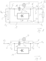
- Fig. 1 shows schematically a separating device 1, which in the exemplary embodiment is connected between a direct voltage source 2 for generating a direct voltage U DC and a direct current I N and a load 3.
- the disconnecting device 1 comprises, in a main current or positive path 4 representing the positive pole, a protective switch arrangement in the form of a series connection of two magnetic, in particular hydraulic-magnetic, protective switches 5, 6, the switching contacts of which are coupled to a switching lock 7 and are designated C 1 and C 2 .
- Another circuit breaker 8 or switching contact C 3 is connected to the reverse current or negative path (return line) 9 of the separating device 1 and is also coupled to the switching lock 7.
- Semiconductor electronics 10 are connected in parallel to one of the circuit breakers 5, 6, 8, here the circuit breaker 5 or its switching contact C1 .
- the circuit breakers 5, 6, 8 and the semiconductor electronics 10 form a self-sufficient hybrid circuit breaker as a separating device 1 for nominal DC currents (direct currents) I N between 4A DC and 25oA DC at a DC voltage U DC between 300V DC and 1500V DC .
- the semiconductor electronics 10 essentially comprises at least one semiconductor switch 10a, 10b, which is connected in parallel with the circuit breaker 5 of the circuit breaker arrangement 5, 6, 8.
- the gate of an IGBT preferably used as a semiconductor switch 10b, forms the control input or a control connection 11 of the semiconductor circuit 10. This control input or control connection 11 can be routed to the main current path 4 via a control circuit.
- FIG. 1 a four-pole disconnecting device 1 or a four-pole hybrid circuit breaker with supply-side inputs or input connections E 1 and E 2 and load-side outputs or output connections A 1 and A 2 is shown in Figure 2 a two-pole disconnecting device 1 not according to the invention or a two-pole hybrid circuit breaker is shown.
- the respective circuit breakers 5, 6, 8 or their switching contacts C 1 , C 2 , C 3 can each have a switching lock 7 and a magnetic or magnetic-hydraulic trigger 12.
- the circuit breakers 5, 6, 8 are assigned a common switching lock 7 and a common trigger (triggering device) 12.
- the switching contacts C n of the further circuit breakers are then preferably mechanically coupled to the switching lock 7 of the main circuit breaker, here the circuit breaker 5, in order to at least approximately simultaneously trigger the circuit breakers 5, 6, 8 and contact separation of the switch contacts C n of all circuit breakers 5, 6, 8 the circuit breaker arrangement.
- the circuit breakers 5, 6, 8 or their switching contacts C n are assigned a drive 13 designed as a motor or magnet system.
- a control signal S A for triggering the circuit breaker is supplied to this by a module 14, hereinafter referred to as Arc Fault Module, for arc detection or for detecting an overcurrent.
- the module 14 is connected to a current sensor 15, which detects the current I flowing preferably in the main current path 4. The detected current I is evaluated using the module 14.
- the module 14 the control or trigger signal S A is generated.
- the circuit breakers 5, 6, 8 of the circuit breaker arrangement are triggered practically at the same time.
- An arc created in the course of opening the switching contacts C n causes a corresponding arc voltage and a corresponding arc current, which switches the previously current-blocking semiconductor electronics 10 to conduct current, so that the current flowing in the main current path 4 commutates to the semiconductor electronics 10 and is taken over by it until the arc goes out becomes.
- the semiconductor electronics 10 accepts switching currents up to a value of approximately 1000A within a very short period of time, with the commutation being dependent on the circuit inductance within a corresponding time range of 50 ⁇ s to 300 ⁇ s. At higher switching currents, the circuit breaker arrangement 5, 6, 8 alone takes over the shutdown and current limitation.
- Fig. 4 shows the circuit of a possible, preferably used semiconductor electronics 10, which is connected in parallel to the circuit breaker 5 of the circuit breaker arrangement 5, 6, 8 of the self-sufficient hybrid circuit breaker as a disconnecting device 1.
- a first semiconductor switch (IGBT) 10a is connected in series in a cascode arrangement with a second semiconductor switch 10b in the form of a MOSFET.
- the cascode arrangement with the two semiconductor switches 10a, 10b thus forms analogous to Fig. 1 the commutation path 16 which is parallel to the circuit breaker 5 of the circuit breaker arrangement 5, 6, 8 and thus to the main current path 4.
- the first semiconductor switch 10a is led between the direct current source 2 and the circuit breaker arrangement and there parallel to the switching contact C1 to the main current path 4.
- the potential U+ is always greater than the potential U- on the opposite side of the switch, on which the second semiconductor switch (MOSFET) 10b is connected to the main circuit 4.
- the plus potential U+ is 0V when the switching contacts C n of the circuit breaker arrangement 5, 6, 8 are closed.
- the first semiconductor switch (IGBT) 10a is connected to a freewheeling diode D2.
- a first tens diode D3 is connected on the anode side to the potential U and on the cathode side to the gate (control input 11) of the first semiconductor switch (IGBT) 10a.
- Another tens diode D4 is again connected to the cathode side Control input 11 and connected on the anode side to the emitter of the first semiconductor switch (IGBT) 10a.
- a diode D1 is connected on the anode side to a center or cascode tap 17 between the first and second semiconductor switches 10a and 10b of the cascode arrangement, which is connected to the potential U- on the cathode side via a capacitor C serving as an energy storage device.
- a transistor T1 connected to ohmic resistors R1 and R2 is connected via further resistors R3 and R4 to the gate of the second semiconductor switch 10b, which is in turn connected to the control input 12 of the semiconductor electronics 10 tied together.
- a further tens diode D5 with a parallel resistor R5 is connected on the cathode side to the gate and on the anode side to the emitter of the second semiconductor switch 10b.
- the transistor T1 On the base side, the transistor T1 is controlled via a transistor T2, which in turn is connected on the base side via an ohmic resistor R6 to a timing element 19, for example designed as a monoflop. On the base-emitter side, the transistor T2 is also connected to another resistor R7.
- the commutation of the switch current I which essentially corresponds to the arc current, from the main current path 4 to the commutation path 16 of the semiconductor electronics 10 begins practically the arc current between the main current path 4, i.e. via the circuit breakers 5, 6, 8 and the commutation path 16, i.e. the semiconductor electronics 10.
- the energy storage device C is charged during this arc time interval.
- the period of time is set in such a way that, on the one hand, sufficient energy is available for reliable activation of the semiconductor electronics 10, in particular for switching it off during a certain period of time following the period of time representing the arc duration.
- the period of time is sufficiently short so that undesirable contact erosion or wear of the switching contacts C n of the circuit breaker arrangement 5, 6, 8 is avoided.
- the first semiconductor switch 10a is controlled via the resistor R at least to such an extent that a sufficient charging voltage and a sufficient arc or charging current are available for the capacitors C.
- U Ab 12V (DC)
- the tap voltage serves to supply the control circuit of the electronics 10, which is essentially formed by the transistors T1 and T2 as well as the timing element 19 and the energy storage C.
- the diode D1 which is connected on the anode side to the cascode tap 17 and on the cathode side to the capacitor C, prevents the charging current from flowing back from the Capacitors C and via the commutation path 16 in the direction of the potential U-.
- the charging capacity and thus the storage energy contained in the capacitor C is dimensioned such that the semiconductor electronics 10 the switch current I for carries a period of time specified by the timer 19.
- This time period can be set to, for example, 3ms.
- the dimensioning of this time period and thus the determination of the timer 19 are essentially based on the application-specific or typical time periods for the arc to be completely extinguished and for the plasma formed to have cooled down sufficiently.
- the essential requirement here is that after the electronics 10 has been switched off, with the then again high-resistance commutation path 16 and consequently current-blocking semiconductor electronics 10, no new arc can occur on the circuit breaker arrangement 5, 6, 8, which is still triggered.
- the plus potential U+ thus goes against this operating voltage when the commutation path 16 becomes high-resistance due to the blocking of the semiconductor switches 10 and thus the electronics 10 becomes current-blocking again.
- an electrical device e.g. B. an inverter of a photovoltaic system can be provided.
Landscapes
- Driving Mechanisms And Operating Circuits Of Arc-Extinguishing High-Tension Switches (AREA)
- Emergency Protection Circuit Devices (AREA)
- Keying Circuit Devices (AREA)
Applications Claiming Priority (3)
| Application Number | Priority Date | Filing Date | Title |
|---|---|---|---|
| DE102014008706.9A DE102014008706A1 (de) | 2014-06-18 | 2014-06-18 | Trennschalter zur Gleichstromunterbrechung |
| PCT/EP2015/000576 WO2015192924A1 (de) | 2014-06-18 | 2015-03-16 | Trennschalter zur gleichstromunterbrechung |
| EP15714411.4A EP3158571B1 (de) | 2014-06-18 | 2015-03-16 | Trennschalter zur gleichstromunterbrechung |
Related Parent Applications (2)
| Application Number | Title | Priority Date | Filing Date |
|---|---|---|---|
| EP15714411.4A Division EP3158571B1 (de) | 2014-06-18 | 2015-03-16 | Trennschalter zur gleichstromunterbrechung |
| EP15714411.4A Division-Into EP3158571B1 (de) | 2014-06-18 | 2015-03-16 | Trennschalter zur gleichstromunterbrechung |
Publications (3)
| Publication Number | Publication Date |
|---|---|
| EP3855465A1 EP3855465A1 (de) | 2021-07-28 |
| EP3855465B1 true EP3855465B1 (de) | 2023-10-11 |
| EP3855465C0 EP3855465C0 (de) | 2023-10-11 |
Family
ID=52814044
Family Applications (2)
| Application Number | Title | Priority Date | Filing Date |
|---|---|---|---|
| EP20207521.4A Active EP3855465B1 (de) | 2014-06-18 | 2015-03-16 | Trennschalter zur gleichstromunterbrechung |
| EP15714411.4A Active EP3158571B1 (de) | 2014-06-18 | 2015-03-16 | Trennschalter zur gleichstromunterbrechung |
Family Applications After (1)
| Application Number | Title | Priority Date | Filing Date |
|---|---|---|---|
| EP15714411.4A Active EP3158571B1 (de) | 2014-06-18 | 2015-03-16 | Trennschalter zur gleichstromunterbrechung |
Country Status (6)
| Country | Link |
|---|---|
| US (1) | US10931093B2 (https=) |
| EP (2) | EP3855465B1 (https=) |
| JP (1) | JP2017527067A (https=) |
| CN (1) | CN106663557B (https=) |
| DE (1) | DE102014008706A1 (https=) |
| WO (1) | WO2015192924A1 (https=) |
Families Citing this family (21)
| Publication number | Priority date | Publication date | Assignee | Title |
|---|---|---|---|---|
| DE102015219545B3 (de) * | 2015-10-08 | 2017-01-05 | Ellenberger & Poensgen Gmbh | Elektronischer Schutzschalter |
| WO2017152999A1 (de) * | 2016-03-11 | 2017-09-14 | Siemens Aktiengesellschaft | Schaltanlagenanordnung, umrichteranordnung mit schaltanlagenanordnung und verfahren zum schutz der umrichteranordnung |
| DE102016105544A1 (de) * | 2016-03-24 | 2017-09-28 | Epcos Ag | Vorrichtung zur Messung eines Zustands eines elektrischen Schalters, elektrischer Schalter und Verfahren zur Messung eines Zustands eines elektrischen Schalters |
| DE102017101452A1 (de) | 2017-01-25 | 2018-07-26 | Eaton Industries (Austria) Gmbh | Niederspannungs-Schutzschaltgerät |
| US11189438B2 (en) | 2017-04-26 | 2021-11-30 | Sony Corporation | Arc suppression device, mobile body, and power supply system |
| US10629391B2 (en) | 2017-12-21 | 2020-04-21 | Eaton Intelligent Power Limited | Fusible safety disconnect in solid state circuit breakers and combination motor starters |
| JP7311163B2 (ja) * | 2018-06-27 | 2023-07-19 | ウチヤ・サーモスタット株式会社 | 電子機器 |
| EP3594979A1 (en) * | 2018-07-09 | 2020-01-15 | ABB Schweiz AG | Apparatus to switch a led |
| JP6694177B2 (ja) * | 2018-10-30 | 2020-05-13 | 嶋田 隆一 | 直流遮断装置 |
| US11270854B2 (en) * | 2018-12-26 | 2022-03-08 | Eaton Intelligent Power Limited | Circuit protection devices, systems and methods for explosive environment compliance |
| US11615925B2 (en) | 2018-12-26 | 2023-03-28 | Eaton Intelligent Power Limited | Hazardous location compliant circuit protection devices having enhanced safety intelligence, systems and methods |
| EP3694105A1 (de) | 2019-02-05 | 2020-08-12 | Siemens Aktiengesellschaft | Schaltvorrichtung zum auftrennen eines strompfads |
| EP3925048A1 (de) | 2019-03-29 | 2021-12-22 | Siemens Aktiengesellschaft | Elektrisches netzwerk |
| EP3739707A1 (de) | 2019-05-17 | 2020-11-18 | Siemens Aktiengesellschaft | Überstromschutzvorrichtung für den schutz eines in einem gleichstromnetz angeordneten verbrauchers |
| JP2022550281A (ja) * | 2019-09-17 | 2022-12-01 | エレンベルガー ウント ペンスケン ゲゼルシャフト ミット ベシュレンクテル ハフツング | コントローラと、アクチュエータと、機能的安全性を提供するためのアセンブリと、を含むシステム |
| US11482851B2 (en) * | 2020-10-14 | 2022-10-25 | Eaton Intelligent Power Limited | Arc flash mitigation device |
| ES2956365T3 (es) * | 2020-12-15 | 2023-12-20 | Abb Schweiz Ag | Un aparato de conmutación híbrido para redes eléctricas |
| DE102021113589A1 (de) * | 2021-05-26 | 2022-12-01 | Lisa Dräxlmaier GmbH | Elektronischer stromverteiler |
| CN117981030A (zh) * | 2021-09-30 | 2024-05-03 | 松下知识产权经营株式会社 | 断路装置和驱动装置 |
| DE102022134287B3 (de) * | 2022-12-21 | 2024-01-18 | Semikron Elektronik Gmbh & Co. Kg | Ansteuereinrichtung, Halbbrückenschaltungsanordnung damit und Verfahren dazu |
| US12444919B1 (en) * | 2023-03-28 | 2025-10-14 | Amazon Technologies, Inc. | System for operation of enhanced circuit breakers |
Family Cites Families (24)
| Publication number | Priority date | Publication date | Assignee | Title |
|---|---|---|---|---|
| JPS6178020A (ja) * | 1984-09-26 | 1986-04-21 | 三菱電機株式会社 | 電力開閉装置 |
| US4598330A (en) * | 1984-10-31 | 1986-07-01 | International Business Machines Corporation | High power direct current switching circuit |
| EP0231469B1 (de) * | 1986-01-31 | 1991-07-03 | BBC Brown Boveri AG | Leistungsschalter |
| FR2606929B1 (fr) * | 1986-11-14 | 1989-02-10 | Telemecanique Electrique | Dispositif interrupteur pour appareil de protection |
| US5410442A (en) * | 1992-02-17 | 1995-04-25 | Siemens Aktiengesellschaft | Electromechanical protection devcie |
| US5519561A (en) * | 1994-11-08 | 1996-05-21 | Eaton Corporation | Circuit breaker using bimetal of thermal-magnetic trip to sense current |
| JPH08315666A (ja) | 1995-05-12 | 1996-11-29 | Mitsubishi Electric Corp | 遮断器および遮断装置 |
| DE19619437C2 (de) * | 1996-05-14 | 2003-01-16 | Abb Schweiz Ag | Schaltgerät |
| FR2794890B1 (fr) * | 1999-06-08 | 2001-08-10 | Crouzet Automatismes | Relais electromecanique assiste a la commutation par semi-conducteur |
| KR100434153B1 (ko) * | 2002-04-12 | 2004-06-04 | 엘지산전 주식회사 | 하이브리드 직류 전자 접촉기 |
| JP2006032121A (ja) * | 2004-07-16 | 2006-02-02 | Japan Ae Power Systems Corp | 高電圧大容量遮断器 |
| DE102005006953A1 (de) * | 2005-02-16 | 2006-08-17 | Abb Patent Gmbh | Schaltgerät mit PTC-Element |
| US8879218B2 (en) * | 2007-12-14 | 2014-11-04 | True-Safe Technologies, Inc. | Arc fault circuit interrupter, systems, apparatus and methods of detecting and interrupting electrical faults |
| JP2009206066A (ja) * | 2008-02-27 | 2009-09-10 | Daito Communication Apparatus Co Ltd | ハイブリッド型直流リレー |
| CN101752148B (zh) * | 2008-12-12 | 2014-08-13 | 施耐德电器工业公司 | 带选择性的断路器 |
| DE202009004198U1 (de) | 2009-03-25 | 2010-08-12 | Ellenberger & Poensgen Gmbh | Trennschalter zur galvanischen Gleichstromunterbrechung |
| FR2952470A1 (fr) * | 2009-11-06 | 2011-05-13 | Schneider Electric Ind Sas | Disjoncteur limiteur de courant, dispositif de distribution electrique pourvu d'un tel disjoncteur limiteur et procede de limitation de courant |
| DE102009059839A1 (de) * | 2009-12-21 | 2011-06-22 | Eaton Industries GmbH, 53115 | Vorrichtung zum Erkennen der Stromrichtungsumkehr |
| JP5291660B2 (ja) * | 2010-04-13 | 2013-09-18 | 日本電信電話株式会社 | 遮断装置 |
| JP5669537B2 (ja) * | 2010-11-30 | 2015-02-12 | 富士電機株式会社 | 電力監視制御装置およびブレーカ |
| JP5793019B2 (ja) * | 2011-08-19 | 2015-10-14 | 富士電機株式会社 | 消弧装置および開閉器 |
| DE102011056577C5 (de) * | 2011-12-19 | 2015-02-19 | Sma Solar Technology Ag | Schaltungsanordnung zur Unterdrückung eines bei einem Schaltvorgang auftretenden Lichtbogens |
| DE202012007257U1 (de) | 2012-07-26 | 2013-10-28 | Ellenberger & Poensgen Gmbh | Vorrichtung zum sicheren Schalten einer Photovoltaikanlage |
| DE102013114259A1 (de) * | 2013-12-17 | 2015-06-18 | Eaton Electrical Ip Gmbh & Co. Kg | Schaltvorrichtung zum Führen und Trennen von elektrischen Strömen |
-
2014
- 2014-06-18 DE DE102014008706.9A patent/DE102014008706A1/de not_active Ceased
-
2015
- 2015-03-16 EP EP20207521.4A patent/EP3855465B1/de active Active
- 2015-03-16 EP EP15714411.4A patent/EP3158571B1/de active Active
- 2015-03-16 JP JP2016569977A patent/JP2017527067A/ja active Pending
- 2015-03-16 CN CN201580032448.4A patent/CN106663557B/zh active Active
- 2015-03-16 WO PCT/EP2015/000576 patent/WO2015192924A1/de not_active Ceased
-
2016
- 2016-12-19 US US15/383,416 patent/US10931093B2/en active Active
Also Published As
| Publication number | Publication date |
|---|---|
| EP3158571A1 (de) | 2017-04-26 |
| DE102014008706A1 (de) | 2015-12-24 |
| EP3855465A1 (de) | 2021-07-28 |
| CN106663557A (zh) | 2017-05-10 |
| US10931093B2 (en) | 2021-02-23 |
| US20170098931A1 (en) | 2017-04-06 |
| EP3158571B1 (de) | 2022-08-03 |
| WO2015192924A1 (de) | 2015-12-23 |
| EP3855465C0 (de) | 2023-10-11 |
| CN106663557B (zh) | 2019-05-10 |
| JP2017527067A (ja) | 2017-09-14 |
Similar Documents
| Publication | Publication Date | Title |
|---|---|---|
| EP3855465B1 (de) | Trennschalter zur gleichstromunterbrechung | |
| EP2411990B1 (de) | Trennschalter zur galvanischen gleichstromunterbrechung | |
| DE102016219098B4 (de) | Batterie-Trenneinrichtung | |
| EP3320553B1 (de) | Trennvorrichtung zur gleichstromunterbrechung | |
| DE3735009A1 (de) | Leistungstrennschalter | |
| EP3542386B1 (de) | Niederspannungs-schutzschaltgerät | |
| EP3242399B1 (de) | Monolithisch integrierter halbleiterschalter, insbesondere leistungstrennschalter | |
| DE102016120070A1 (de) | Niederspannungs-Schutzschaltgerät | |
| EP3091550A1 (de) | Hybride sachalteinrichtung | |
| DE102015226475A1 (de) | Schalteinrichtung | |
| EP3915127B1 (de) | Gleichstrom-schutzschaltgerät | |
| DE2135494A1 (de) | Schutzschaltung für einen statischen Schalter | |
| EP3210226B1 (de) | Trennschalter zur galvanischen gleichstromunterbrechung | |
| EP3550582B1 (de) | Niederspannungs-schutzschaltgerät | |
| DE102017122218A1 (de) | Niederspannungs-Schutzschaltgerät | |
| EP3762953B1 (de) | Trennvorrichtung zur gleichstromunterbrechung eines strompfads, und bordnetz eines kraftfahrzeugs | |
| WO2013091689A1 (de) | Trennvorrichtung zur gleichstromunterbrechung zwischen einem photovoltaikgenerator und einer elektrischen einrichtung sowie photovoltaikanlage mit einer derartigen trennvorrichtung | |
| DE3317942A1 (de) | Schaltungsanordnung | |
| LU505555B1 (de) | Trennschalter | |
| DE102020134773A1 (de) | Leistungsschalter für gleichströme | |
| DE102023102240A1 (de) | Gleichspannungsschaltgerät, insbesondere zum Unterbrechen eines Stromflusses, und Gleichspannungssystem |
Legal Events
| Date | Code | Title | Description |
|---|---|---|---|
| PUAI | Public reference made under article 153(3) epc to a published international application that has entered the european phase |
Free format text: ORIGINAL CODE: 0009012 |
|
| STAA | Information on the status of an ep patent application or granted ep patent |
Free format text: STATUS: REQUEST FOR EXAMINATION WAS MADE |
|
| 17P | Request for examination filed |
Effective date: 20201113 |
|
| AC | Divisional application: reference to earlier application |
Ref document number: 3158571 Country of ref document: EP Kind code of ref document: P |
|
| AK | Designated contracting states |
Kind code of ref document: A1 Designated state(s): AL AT BE BG CH CY CZ DE DK EE ES FI FR GB GR HR HU IE IS IT LI LT LU LV MC MK MT NL NO PL PT RO RS SE SI SK SM TR |
|
| GRAP | Despatch of communication of intention to grant a patent |
Free format text: ORIGINAL CODE: EPIDOSNIGR1 |
|
| STAA | Information on the status of an ep patent application or granted ep patent |
Free format text: STATUS: GRANT OF PATENT IS INTENDED |
|
| RIC1 | Information provided on ipc code assigned before grant |
Ipc: H01H 71/10 20060101ALN20230417BHEP Ipc: H01H 9/54 20060101AFI20230417BHEP |
|
| INTG | Intention to grant announced |
Effective date: 20230519 |
|
| GRAS | Grant fee paid |
Free format text: ORIGINAL CODE: EPIDOSNIGR3 |
|
| GRAA | (expected) grant |
Free format text: ORIGINAL CODE: 0009210 |
|
| STAA | Information on the status of an ep patent application or granted ep patent |
Free format text: STATUS: THE PATENT HAS BEEN GRANTED |
|
| AC | Divisional application: reference to earlier application |
Ref document number: 3158571 Country of ref document: EP Kind code of ref document: P |
|
| AK | Designated contracting states |
Kind code of ref document: B1 Designated state(s): AL AT BE BG CH CY CZ DE DK EE ES FI FR GB GR HR HU IE IS IT LI LT LU LV MC MK MT NL NO PL PT RO RS SE SI SK SM TR |
|
| REG | Reference to a national code |
Ref country code: GB Ref legal event code: FG4D Free format text: NOT ENGLISH |
|
| REG | Reference to a national code |
Ref country code: CH Ref legal event code: EP |
|
| REG | Reference to a national code |
Ref country code: DE Ref legal event code: R096 Ref document number: 502015016639 Country of ref document: DE |
|
| REG | Reference to a national code |
Ref country code: IE Ref legal event code: FG4D Free format text: LANGUAGE OF EP DOCUMENT: GERMAN |
|
| U01 | Request for unitary effect filed |
Effective date: 20231012 |
|
| U07 | Unitary effect registered |
Designated state(s): AT BE BG DE DK EE FI FR IT LT LU LV MT NL PT SE SI Effective date: 20231024 |
|
| PG25 | Lapsed in a contracting state [announced via postgrant information from national office to epo] |
Ref country code: GR Free format text: LAPSE BECAUSE OF FAILURE TO SUBMIT A TRANSLATION OF THE DESCRIPTION OR TO PAY THE FEE WITHIN THE PRESCRIBED TIME-LIMIT Effective date: 20240112 |
|
| PG25 | Lapsed in a contracting state [announced via postgrant information from national office to epo] |
Ref country code: IS Free format text: LAPSE BECAUSE OF FAILURE TO SUBMIT A TRANSLATION OF THE DESCRIPTION OR TO PAY THE FEE WITHIN THE PRESCRIBED TIME-LIMIT Effective date: 20240211 |
|
| PG25 | Lapsed in a contracting state [announced via postgrant information from national office to epo] |
Ref country code: ES Free format text: LAPSE BECAUSE OF FAILURE TO SUBMIT A TRANSLATION OF THE DESCRIPTION OR TO PAY THE FEE WITHIN THE PRESCRIBED TIME-LIMIT Effective date: 20231011 |
|
| PG25 | Lapsed in a contracting state [announced via postgrant information from national office to epo] |
Ref country code: IS Free format text: LAPSE BECAUSE OF FAILURE TO SUBMIT A TRANSLATION OF THE DESCRIPTION OR TO PAY THE FEE WITHIN THE PRESCRIBED TIME-LIMIT Effective date: 20240211 Ref country code: GR Free format text: LAPSE BECAUSE OF FAILURE TO SUBMIT A TRANSLATION OF THE DESCRIPTION OR TO PAY THE FEE WITHIN THE PRESCRIBED TIME-LIMIT Effective date: 20240112 Ref country code: ES Free format text: LAPSE BECAUSE OF FAILURE TO SUBMIT A TRANSLATION OF THE DESCRIPTION OR TO PAY THE FEE WITHIN THE PRESCRIBED TIME-LIMIT Effective date: 20231011 |
|
| U20 | Renewal fee for the european patent with unitary effect paid |
Year of fee payment: 10 Effective date: 20240327 |
|
| PG25 | Lapsed in a contracting state [announced via postgrant information from national office to epo] |
Ref country code: RS Free format text: LAPSE BECAUSE OF FAILURE TO SUBMIT A TRANSLATION OF THE DESCRIPTION OR TO PAY THE FEE WITHIN THE PRESCRIBED TIME-LIMIT Effective date: 20231011 Ref country code: PL Free format text: LAPSE BECAUSE OF FAILURE TO SUBMIT A TRANSLATION OF THE DESCRIPTION OR TO PAY THE FEE WITHIN THE PRESCRIBED TIME-LIMIT Effective date: 20231011 Ref country code: NO Free format text: LAPSE BECAUSE OF FAILURE TO SUBMIT A TRANSLATION OF THE DESCRIPTION OR TO PAY THE FEE WITHIN THE PRESCRIBED TIME-LIMIT Effective date: 20240111 Ref country code: HR Free format text: LAPSE BECAUSE OF FAILURE TO SUBMIT A TRANSLATION OF THE DESCRIPTION OR TO PAY THE FEE WITHIN THE PRESCRIBED TIME-LIMIT Effective date: 20231011 |
|
| REG | Reference to a national code |
Ref country code: DE Ref legal event code: R097 Ref document number: 502015016639 Country of ref document: DE |
|
| PG25 | Lapsed in a contracting state [announced via postgrant information from national office to epo] |
Ref country code: CZ Free format text: LAPSE BECAUSE OF FAILURE TO SUBMIT A TRANSLATION OF THE DESCRIPTION OR TO PAY THE FEE WITHIN THE PRESCRIBED TIME-LIMIT Effective date: 20231011 |
|
| PG25 | Lapsed in a contracting state [announced via postgrant information from national office to epo] |
Ref country code: SK Free format text: LAPSE BECAUSE OF FAILURE TO SUBMIT A TRANSLATION OF THE DESCRIPTION OR TO PAY THE FEE WITHIN THE PRESCRIBED TIME-LIMIT Effective date: 20231011 |
|
| PG25 | Lapsed in a contracting state [announced via postgrant information from national office to epo] |
Ref country code: SM Free format text: LAPSE BECAUSE OF FAILURE TO SUBMIT A TRANSLATION OF THE DESCRIPTION OR TO PAY THE FEE WITHIN THE PRESCRIBED TIME-LIMIT Effective date: 20231011 Ref country code: SK Free format text: LAPSE BECAUSE OF FAILURE TO SUBMIT A TRANSLATION OF THE DESCRIPTION OR TO PAY THE FEE WITHIN THE PRESCRIBED TIME-LIMIT Effective date: 20231011 Ref country code: RO Free format text: LAPSE BECAUSE OF FAILURE TO SUBMIT A TRANSLATION OF THE DESCRIPTION OR TO PAY THE FEE WITHIN THE PRESCRIBED TIME-LIMIT Effective date: 20231011 Ref country code: CZ Free format text: LAPSE BECAUSE OF FAILURE TO SUBMIT A TRANSLATION OF THE DESCRIPTION OR TO PAY THE FEE WITHIN THE PRESCRIBED TIME-LIMIT Effective date: 20231011 |
|
| PLBE | No opposition filed within time limit |
Free format text: ORIGINAL CODE: 0009261 |
|
| STAA | Information on the status of an ep patent application or granted ep patent |
Free format text: STATUS: NO OPPOSITION FILED WITHIN TIME LIMIT |
|
| 26N | No opposition filed |
Effective date: 20240712 |
|
| REG | Reference to a national code |
Ref country code: CH Ref legal event code: PL |
|
| PG25 | Lapsed in a contracting state [announced via postgrant information from national office to epo] |
Ref country code: MC Free format text: LAPSE BECAUSE OF FAILURE TO SUBMIT A TRANSLATION OF THE DESCRIPTION OR TO PAY THE FEE WITHIN THE PRESCRIBED TIME-LIMIT Effective date: 20231011 |
|
| GBPC | Gb: european patent ceased through non-payment of renewal fee |
Effective date: 20240316 |
|
| PG25 | Lapsed in a contracting state [announced via postgrant information from national office to epo] |
Ref country code: MC Free format text: LAPSE BECAUSE OF FAILURE TO SUBMIT A TRANSLATION OF THE DESCRIPTION OR TO PAY THE FEE WITHIN THE PRESCRIBED TIME-LIMIT Effective date: 20231011 |
|
| PG25 | Lapsed in a contracting state [announced via postgrant information from national office to epo] |
Ref country code: GB Free format text: LAPSE BECAUSE OF NON-PAYMENT OF DUE FEES Effective date: 20240316 |
|
| PG25 | Lapsed in a contracting state [announced via postgrant information from national office to epo] |
Ref country code: IE Free format text: LAPSE BECAUSE OF NON-PAYMENT OF DUE FEES Effective date: 20240316 |
|
| PG25 | Lapsed in a contracting state [announced via postgrant information from national office to epo] |
Ref country code: IE Free format text: LAPSE BECAUSE OF NON-PAYMENT OF DUE FEES Effective date: 20240316 Ref country code: GB Free format text: LAPSE BECAUSE OF NON-PAYMENT OF DUE FEES Effective date: 20240316 Ref country code: CH Free format text: LAPSE BECAUSE OF NON-PAYMENT OF DUE FEES Effective date: 20240331 |
|
| U20 | Renewal fee for the european patent with unitary effect paid |
Year of fee payment: 11 Effective date: 20250326 |
|
| PG25 | Lapsed in a contracting state [announced via postgrant information from national office to epo] |
Ref country code: CY Free format text: LAPSE BECAUSE OF FAILURE TO SUBMIT A TRANSLATION OF THE DESCRIPTION OR TO PAY THE FEE WITHIN THE PRESCRIBED TIME-LIMIT; INVALID AB INITIO Effective date: 20150316 |
|
| PG25 | Lapsed in a contracting state [announced via postgrant information from national office to epo] |
Ref country code: HU Free format text: LAPSE BECAUSE OF FAILURE TO SUBMIT A TRANSLATION OF THE DESCRIPTION OR TO PAY THE FEE WITHIN THE PRESCRIBED TIME-LIMIT; INVALID AB INITIO Effective date: 20150316 |
|
| PG25 | Lapsed in a contracting state [announced via postgrant information from national office to epo] |
Ref country code: TR Free format text: LAPSE BECAUSE OF FAILURE TO SUBMIT A TRANSLATION OF THE DESCRIPTION OR TO PAY THE FEE WITHIN THE PRESCRIBED TIME-LIMIT Effective date: 20231011 |