EP3842233B1 - Flüssigkeitsausstossvorrichtung, treiberschaltung und integrierte schaltung - Google Patents
Flüssigkeitsausstossvorrichtung, treiberschaltung und integrierte schaltung Download PDFInfo
- Publication number
- EP3842233B1 EP3842233B1 EP20217215.1A EP20217215A EP3842233B1 EP 3842233 B1 EP3842233 B1 EP 3842233B1 EP 20217215 A EP20217215 A EP 20217215A EP 3842233 B1 EP3842233 B1 EP 3842233B1
- Authority
- EP
- European Patent Office
- Prior art keywords
- circuit
- signal
- drive
- voltage
- modulation
- Prior art date
- Legal status (The legal status is an assumption and is not a legal conclusion. Google has not performed a legal analysis and makes no representation as to the accuracy of the status listed.)
- Active
Links
Images



Classifications
-
- H—ELECTRICITY
- H03—ELECTRONIC CIRCUITRY
- H03F—AMPLIFIERS
- H03F3/00—Amplifiers with only discharge tubes or only semiconductor devices as amplifying elements
- H03F3/20—Power amplifiers, e.g. Class B amplifiers, Class C amplifiers
- H03F3/21—Power amplifiers, e.g. Class B amplifiers, Class C amplifiers with semiconductor devices only
- H03F3/217—Class D power amplifiers; Switching amplifiers
- H03F3/2173—Class D power amplifiers; Switching amplifiers of the bridge type
-
- B—PERFORMING OPERATIONS; TRANSPORTING
- B41—PRINTING; LINING MACHINES; TYPEWRITERS; STAMPS
- B41J—TYPEWRITERS; SELECTIVE PRINTING MECHANISMS, i.e. MECHANISMS PRINTING OTHERWISE THAN FROM A FORME; CORRECTION OF TYPOGRAPHICAL ERRORS
- B41J2/00—Typewriters or selective printing mechanisms characterised by the printing or marking process for which they are designed
- B41J2/005—Typewriters or selective printing mechanisms characterised by the printing or marking process for which they are designed characterised by bringing liquid or particles selectively into contact with a printing material
- B41J2/01—Ink jet
- B41J2/015—Ink jet characterised by the jet generation process
- B41J2/04—Ink jet characterised by the jet generation process generating single droplets or particles on demand
- B41J2/045—Ink jet characterised by the jet generation process generating single droplets or particles on demand by pressure, e.g. electromechanical transducers
- B41J2/04501—Control methods or devices therefor, e.g. driver circuits, control circuits
- B41J2/04541—Specific driving circuit
-
- B—PERFORMING OPERATIONS; TRANSPORTING
- B41—PRINTING; LINING MACHINES; TYPEWRITERS; STAMPS
- B41J—TYPEWRITERS; SELECTIVE PRINTING MECHANISMS, i.e. MECHANISMS PRINTING OTHERWISE THAN FROM A FORME; CORRECTION OF TYPOGRAPHICAL ERRORS
- B41J2/00—Typewriters or selective printing mechanisms characterised by the printing or marking process for which they are designed
- B41J2/005—Typewriters or selective printing mechanisms characterised by the printing or marking process for which they are designed characterised by bringing liquid or particles selectively into contact with a printing material
- B41J2/01—Ink jet
- B41J2/015—Ink jet characterised by the jet generation process
- B41J2/04—Ink jet characterised by the jet generation process generating single droplets or particles on demand
- B41J2/045—Ink jet characterised by the jet generation process generating single droplets or particles on demand by pressure, e.g. electromechanical transducers
- B41J2/04501—Control methods or devices therefor, e.g. driver circuits, control circuits
- B41J2/04581—Control methods or devices therefor, e.g. driver circuits, control circuits controlling heads based on piezoelectric elements
-
- B—PERFORMING OPERATIONS; TRANSPORTING
- B41—PRINTING; LINING MACHINES; TYPEWRITERS; STAMPS
- B41J—TYPEWRITERS; SELECTIVE PRINTING MECHANISMS, i.e. MECHANISMS PRINTING OTHERWISE THAN FROM A FORME; CORRECTION OF TYPOGRAPHICAL ERRORS
- B41J2/00—Typewriters or selective printing mechanisms characterised by the printing or marking process for which they are designed
- B41J2/005—Typewriters or selective printing mechanisms characterised by the printing or marking process for which they are designed characterised by bringing liquid or particles selectively into contact with a printing material
- B41J2/01—Ink jet
- B41J2/015—Ink jet characterised by the jet generation process
- B41J2/04—Ink jet characterised by the jet generation process generating single droplets or particles on demand
- B41J2/045—Ink jet characterised by the jet generation process generating single droplets or particles on demand by pressure, e.g. electromechanical transducers
- B41J2/04501—Control methods or devices therefor, e.g. driver circuits, control circuits
- B41J2/04588—Control methods or devices therefor, e.g. driver circuits, control circuits using a specific waveform
-
- B—PERFORMING OPERATIONS; TRANSPORTING
- B41—PRINTING; LINING MACHINES; TYPEWRITERS; STAMPS
- B41J—TYPEWRITERS; SELECTIVE PRINTING MECHANISMS, i.e. MECHANISMS PRINTING OTHERWISE THAN FROM A FORME; CORRECTION OF TYPOGRAPHICAL ERRORS
- B41J2/00—Typewriters or selective printing mechanisms characterised by the printing or marking process for which they are designed
- B41J2/005—Typewriters or selective printing mechanisms characterised by the printing or marking process for which they are designed characterised by bringing liquid or particles selectively into contact with a printing material
- B41J2/01—Ink jet
- B41J2/015—Ink jet characterised by the jet generation process
- B41J2/04—Ink jet characterised by the jet generation process generating single droplets or particles on demand
- B41J2/045—Ink jet characterised by the jet generation process generating single droplets or particles on demand by pressure, e.g. electromechanical transducers
- B41J2/04501—Control methods or devices therefor, e.g. driver circuits, control circuits
- B41J2/04593—Dot-size modulation by changing the size of the drop
-
- B—PERFORMING OPERATIONS; TRANSPORTING
- B41—PRINTING; LINING MACHINES; TYPEWRITERS; STAMPS
- B41J—TYPEWRITERS; SELECTIVE PRINTING MECHANISMS, i.e. MECHANISMS PRINTING OTHERWISE THAN FROM A FORME; CORRECTION OF TYPOGRAPHICAL ERRORS
- B41J2/00—Typewriters or selective printing mechanisms characterised by the printing or marking process for which they are designed
- B41J2/005—Typewriters or selective printing mechanisms characterised by the printing or marking process for which they are designed characterised by bringing liquid or particles selectively into contact with a printing material
- B41J2/01—Ink jet
- B41J2/015—Ink jet characterised by the jet generation process
- B41J2/04—Ink jet characterised by the jet generation process generating single droplets or particles on demand
- B41J2/045—Ink jet characterised by the jet generation process generating single droplets or particles on demand by pressure, e.g. electromechanical transducers
- B41J2/04501—Control methods or devices therefor, e.g. driver circuits, control circuits
- B41J2/04596—Non-ejecting pulses
-
- B—PERFORMING OPERATIONS; TRANSPORTING
- B41—PRINTING; LINING MACHINES; TYPEWRITERS; STAMPS
- B41J—TYPEWRITERS; SELECTIVE PRINTING MECHANISMS, i.e. MECHANISMS PRINTING OTHERWISE THAN FROM A FORME; CORRECTION OF TYPOGRAPHICAL ERRORS
- B41J2/00—Typewriters or selective printing mechanisms characterised by the printing or marking process for which they are designed
- B41J2/005—Typewriters or selective printing mechanisms characterised by the printing or marking process for which they are designed characterised by bringing liquid or particles selectively into contact with a printing material
- B41J2/01—Ink jet
- B41J2/135—Nozzles
- B41J2/14—Structure thereof only for on-demand ink jet heads
- B41J2002/14491—Electrical connection
-
- H—ELECTRICITY
- H03—ELECTRONIC CIRCUITRY
- H03F—AMPLIFIERS
- H03F2200/00—Indexing scheme relating to amplifiers
- H03F2200/351—Pulse width modulation being used in an amplifying circuit
-
- H—ELECTRICITY
- H03—ELECTRONIC CIRCUITRY
- H03K—PULSE TECHNIQUE
- H03K7/00—Modulating pulses with a continuously-variable modulating signal
- H03K7/08—Duration or width modulation ; Duty cycle modulation
Definitions
- a printing apparatus as an example of a liquid ejecting apparatus is an ink jet printer that prints an image including characters, figures, and the like according to image data on a medium such as paper by ejecting ink from a nozzle according to the image data input from an external host computer or the like.
- the ink when ink is ejected from the head unit 20 at the timing when the medium P is transported by the transport mechanism 4, the ink lands on a desired position on the medium P, as a result, an image is formed on the surface of the medium P.
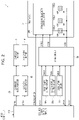
- FIG. 9 is a diagram illustrating a functional configuration of the drive circuit 50.
- the drive circuit 50 includes a power supply voltage control circuit 70, fuses 80 and 81, a drive control circuit 51, and other circuit elements. Then, the drive circuit 50 outputs the drive signal COM for driving the piezoelectric element 60 in the print head 21. In other words, the drive circuit 50 outputs the drive signal COM that is the basis of the drive signal VOUT for operating the piezoelectric element 60 in the print head 21.
- the voltage signal VHVla is input to the inrush current reduction circuit 73.
- the transistor 731 since the transistor 731 is controlled to be non-conductive, the voltage signal VHVla is input to the drain terminal of the transistor 731 as the voltage signal VHVa via the resistor 733. At this time, the current generated due to the voltage signal VHVla and the voltage signal VHVa is limited by the resistor 733. Therefore, the possibility that a large inrush current may occur is reduced.
- the amplified modulation signal AMs generated by the amplifier circuit 550 is input to the demodulation circuit 560.
- the demodulation circuit 560 includes a coil 561 and a capacitor 562. One end of the coil 561 is electrically coupled to the source terminal of the transistor 551 and the drain terminal of the transistor 552. The other end of the coil 561 is electrically coupled to one end of the capacitor 562. The ground potential is supplied to the other end of the capacitor 562. That is, the coil 561 and the capacitor 562 form a low pass filter. Then, the amplified modulation signal AMs is supplied to the demodulation circuit 560, so that the amplified modulation signal AMs is demodulated and the drive signal COM is generated. That is, the demodulation circuit 560 demodulates the amplified modulation signal AMs and outputs the drive signal COM from a terminal COM-Out.
- the amplification control signal generation circuit 502, the amplifier circuit 550, the demodulation circuit 560, and the feedback circuit 570 configured as described above output, as the drive signal COM, a signal including the trapezoidal waveforms Adp, Bdp, and Cdp illustrated in FIG. 3 for driving the piezoelectric element 60 based on the drive data signal DATA. Moreover, it is also possible to output a signal having a constant voltage value as the drive signal COM.
- the control signal CNT1 is input to the drive signal discharge circuit 450.
- the drive signal discharge circuit 450 controls whether or not to discharge the stored charge based on the drive signal COM output from the demodulation circuit 560 via the feedback circuit 570.
- the drive signal discharge circuit 450 is electrically coupled to the propagation path through which the drive signal COM output from the demodulation circuit 560 is propagated via the terminal VFB-In and the feedback circuit 570. That is, the drive signal discharge circuit 450 discharges the charge based on the drive signal COM.
- One end of the resistor 451 is electrically coupled to the terminal VFB-In.
- the other end of the resistor 451 is electrically coupled to a drain terminal of the transistor 452.
- the ground potential is supplied to a source terminal of the transistor 452.
- the control signal CNT1 is input to a gate terminal of the transistor 452 via the inverter 453.
- the control signal CNT1 of H level is input to the drive signal discharge circuit 450 configured as described above, the transistor 452 is controlled to be non-conductive. Therefore, the drive signal discharge circuit 450 does not perform discharge of the charge stored in the propagation path through which the drive signal COM is propagated.
- the control signal CNT1 of L level is input to the drive signal discharge circuit 450, the transistor 452 is controlled to be conductive.
- the sleep mode is likely to continue for a long time as compared with the standby mode.
- the charges of the electrodes 611 and 612 of the piezoelectric element 60 are discharged, and the potential supplied to the electrodes 611 and 612 of the piezoelectric element 60 is set to the ground potential, whereby unintended charges are not stored in the electrodes 611 and 612 of the piezoelectric element 60, and as a result, the possibility that the piezoelectric element 60 is continuously displaced unintentionally is reduced. Thereby, the possibility that the piezoelectric element 60 and the ejection portion 600 will become abnormal due to continuous unintended displacement of the piezoelectric element 60 is reduced.
- the liquid ejecting apparatus 1 transitions to the sleep mode, the register control circuit 440 outputs the control signal CNT1 of H level to the drive signal discharge circuit 450, and outputs the control signal CNT2 of H level to the reference voltage signal output circuit 460, and then, the constant voltage output circuit 420 may output the voltage signal VCNT having a constant voltage value at the ground potential.
- the register control circuit 440 outputs the control signal CNT1 of H level to the drive signal discharge circuit 450, and outputs the control signal CNT2 of H level to the reference voltage signal output circuit 460, and then, the constant voltage output circuit 420 may stop operating.
- the substrate 700 in the integrated circuit 500 is provided with a plurality of terminals for electrically coupling to an internal circuit of the integrated circuit 500 and an external circuit of the integrated circuit 500.
- the substrate 700 in the integrated circuit 500 according to the present embodiment is provided with a plurality of terminals including the terminals CLK-In, DATA-In, Hg-Out, Lg-Out, VFB-In, and VBS-Out illustrated in FIG.
- the first gate drive circuit mounting area 740 among the plurality of circuit mounting areas provided on the substrate 700 is located on the side 704 side of the discharge circuit mounting area 710 and the constant voltage circuit mounting area 720 and on the side 702 side of the terminal Lg-Out.
- the first gate drive circuit mounting area 740 is located in the vicinity of the terminal Lg-Out.
- a circuit that outputs the amplification control signal Lgd in the gate drive circuit 540 illustrated in FIG. 13 is mounted. With the configuration, it is possible to shorten the length of the wiring through which the amplification control signal Lgd is propagated inside the integrated circuit 500.
- the logic circuit mounting area 790 among the plurality of circuit mounting areas provided on the substrate 700 is located on the side 702 side of the modulation circuit mounting area 730, the DAC circuit mounting area 780, the reference voltage circuit mounting area 760, and the internal voltage circuit mounting area 770.
- the terminals DATA-In and CLK-In are located on the side 703 side of the logic circuit mounting area 790.
- the plurality of logic circuits including the register control circuit 440, the VHV control signal output circuit 470, the status signal input/output circuit 480, and the error signal input/output circuit 490 illustrated in FIG. 13 are mounted.
- the voltage signal VCNT output from the constant voltage output circuit 420 is output to the outside of the integrated circuit 500 via the terminal VFB-In
- the drive signal discharge circuit 450 discharges the charge based on the drive signal COM via the terminal VFB-In
- the feedback signal VFB is input to the modulation circuit 530 via the terminal VFB-In. That is, the terminal VFB-In is electrically coupled to the constant voltage output circuit 420, the drive signal discharge circuit 450, and the modulation circuit 530, and the constant voltage output circuit 420, the drive signal discharge circuit 450, and the modulation circuit 530 are electrically coupled to each other.
- the voltage signal VCNT output from the constant voltage output circuit 420, the feedback signal VFB input to the modulation circuit 530, and the charge based on the drive signal COM discharged by the drive signal discharge circuit 450 are propagated through the wiring 741, and the voltage signal VSET output from the modulation circuit 530 is propagated through the wiring 742.
- each of the discharge circuit mounting area 710, the constant voltage circuit mounting area 720, and the modulation circuit mounting area 730 is located so that the distance from the terminal VFB-In becomes longer in the order of the modulation circuit mounting area 730, the constant voltage circuit mounting area 720, and the discharge circuit mounting area 710. That is, of the discharge circuit mounting area 710, the constant voltage circuit mounting area 720, and the modulation circuit mounting area 730, the modulation circuit mounting area 730 is located closest to the terminal VFB-In, the constant voltage circuit mounting area 720 is located in the vicinity of the terminal VFB-In next to the modulation circuit mounting area 730, and the discharge circuit mounting area 710 is located farthest from the terminal VFB-In.
- the possibility that the wiring length of the wiring 741 for electrically coupling the terminal VFB-In, the discharge circuit mounting area 710, the constant voltage circuit mounting area 720, and the modulation circuit mounting area 730 to each another becomes long is reduced, and the possibility that noise generated in the first gate drive circuit mounting area 740 that is not electrically coupled to the wiring 741 on the wiring 741 is superimposed on the discharge circuit mounting area 710, the constant voltage circuit mounting area 720, the modulation circuit mounting area 730, and the wiring 741 is reduced.
- the modulation circuit mounting area 730 in which the modulation circuit 530 is mounted, the constant voltage circuit mounting area 720 in which the constant voltage output circuit 420 is mounted, and the first gate drive circuit mounting area 740 in which the gate drive circuit 540 is mounted are provided side by side in the order of the modulation circuit mounting area 730, the constant voltage circuit mounting area 720, and the first gate drive circuit mounting area 740 in the direction along a virtual straight line IL6.
Landscapes
- Engineering & Computer Science (AREA)
- Power Engineering (AREA)
- Particle Formation And Scattering Control In Inkjet Printers (AREA)
Claims (7)
- Integrierte Schaltung, die in einer Antriebsschaltung verwendet wird, die ein Antriebssignal zum Antreiben einer kapazitiven Last ausgibt, wobei die integrierte Schaltung dadurch gekennzeichnet ist, dass sie umfasst:eine Modulationsschaltung (530), die ein Basisantriebssignal moduliert, um ein Modulationssignal auszugeben;einen Schaltkreis (540), der ein Verstärkungssteuersignal gemäß dem Modulationssignal ausgibt;einen Eingangsanschluss, an den ein Rückkopplungssignal, das auf dem Antriebssignal basiert, eingegeben wird; undeine Konstantspannung-Ausgabeschaltung (420), die ein Gleichspannungssignal ausgibt, wobeidie Modulationsschaltung und die Konstantspannung-Ausgabeschaltung elektrisch an den Eingangsanschluss gekoppelt sind,ein erstes virtuelles Leitungssegment (151), das zwischen dem Eingangsanschluss und der Konstantspannung-Ausgabeschaltung in einer ersten virtuellen geraden Linie liegt, die den Eingangsanschluss und die Konstantspannung-Ausgabeschaltung bei einem kürzesten Abstand verbindet, der die Modulationsschaltung nicht schneidet, undein zweites virtuelles Leitungssegment (153), das zwischen dem Eingangsanschluss und der Modulationsschaltung in einer zweiten virtuellen geraden Linie liegt, die den Eingangsanschluss und die Modulationsschaltung bei einem kürzesten Abstand verbindet, der die Konstantspannung-Ausgabeschaltung nicht schneidet.
- Flüssigkeitsausstoßvorrichtung, dadurch gekennzeichnet, dass sie umfasst:einen Flüssigkeitsausstoßkopf (21) mit einem Antriebselement (60) und der eine Flüssigkeit durch Zuleiten eines Antriebssignals (VOUT) zu dem Antriebselement (60) ausstößt; undeine Antriebsschaltung (50), die das Antriebssignal ausgibt, wobeidie Antriebsschaltung enthält:eine integrierte Schaltung (500) nach Anspruch 1, die ein Verstärkungssteuersignal ausgibt, das auf einem Basisantriebssignal basiert;eine Verstärkerschaltung (550), die gemäß dem Verstärkungssteuersignal arbeitet, um ein verstärktes Modulationssignal auszugeben;eine Demodulationsschaltung (560), die das verstärkte Modulationssignal demoduliert, um das Antriebssignal auszugeben; undeine Rückkopplungsschaltung (570), die ein Rückkopplungssignal, das auf dem Antriebssignal basiert, zu der integrierten Schaltung rückkoppelt.
- Flüssigkeitsausstoßvorrichtung nach Anspruch 2, wobei der kürzeste Abstand zwischen dem Eingangsanschluss und der Modulationsschaltung (530) kürzer ist als der kürzeste Abstand zwischen dem Eingangsanschluss und der Konstantspannung-Ausgabeschaltung (420).
- Flüssigkeitsausstoßvorrichtung nach Anspruch 2, wobei
der Eingangsanschluss zwischen der Modulationsschaltung (530) und der Konstantspannung-Ausgabeschaltung (420) liegt. - Flüssigkeitsausstoßvorrichtung nach Anspruch 2, wobei
das erste virtuelle Leitungssegment (151) den Schaltkreis (540) nicht schneidet. - Flüssigkeitsausstoßvorrichtung nach Anspruch 2, wobei
das zweite virtuelle Leitungssegment (153) den Schaltkreis (540) nicht schneidet. - Antriebsschaltung, die ein Antriebssignal zum Antreiben einer kapazitiven Last ausgibt, wobei die Antriebsschaltung dadurch gekennzeichnet ist, dass sie umfasst:eine integrierte Schaltung (500) nach Anspruch 1, die ein Verstärkungssteuersignal ausgibt, das auf einem Basisantriebssignal basiert;eine Verstärkerschaltung (550), die gemäß dem Verstärkungssteuersignal arbeitet, um ein verstärktes Modulationssignal auszugeben;eine Demodulationsschaltung (560), die das verstärkte Modulationssignal demoduliert, um das Antriebssignal auszugeben; undeine Rückkopplungsschaltung (570), die ein Rückkopplungssignal, das auf dem Antriebssignal basiert, zu der integrierten Schaltung rückkoppelt.
Applications Claiming Priority (1)
| Application Number | Priority Date | Filing Date | Title |
|---|---|---|---|
| JP2019236570A JP7363472B2 (ja) | 2019-12-26 | 2019-12-26 | 液体吐出装置、駆動回路、及び集積回路 |
Publications (2)
| Publication Number | Publication Date |
|---|---|
| EP3842233A1 EP3842233A1 (de) | 2021-06-30 |
| EP3842233B1 true EP3842233B1 (de) | 2022-11-23 |
Family
ID=73943165
Family Applications (1)
| Application Number | Title | Priority Date | Filing Date |
|---|---|---|---|
| EP20217215.1A Active EP3842233B1 (de) | 2019-12-26 | 2020-12-24 | Flüssigkeitsausstossvorrichtung, treiberschaltung und integrierte schaltung |
Country Status (3)
| Country | Link |
|---|---|
| US (1) | US11446924B2 (de) |
| EP (1) | EP3842233B1 (de) |
| JP (1) | JP7363472B2 (de) |
Family Cites Families (11)
| Publication number | Priority date | Publication date | Assignee | Title |
|---|---|---|---|---|
| JP4735279B2 (ja) | 2006-01-17 | 2011-07-27 | 富士ゼロックス株式会社 | 液滴吐出ヘッドの駆動回路及び方法、液滴吐出装置 |
| JP6421560B2 (ja) * | 2014-11-25 | 2018-11-14 | セイコーエプソン株式会社 | 液体吐出装置、ヘッドユニット、容量性負荷駆動用集積回路装置および容量性負荷駆動回路 |
| JP6347327B2 (ja) * | 2014-12-10 | 2018-06-27 | セイコーエプソン株式会社 | 液体吐出装置、ヘッドユニット、容量性負荷駆動回路および容量性負荷駆動用集積回路装置 |
| JP6372333B2 (ja) * | 2014-12-11 | 2018-08-15 | セイコーエプソン株式会社 | 液体吐出装置、ヘッドユニット、容量性負荷駆動用集積回路装置および容量性負荷駆動回路 |
| JP6365281B2 (ja) * | 2014-12-11 | 2018-08-01 | セイコーエプソン株式会社 | 液体吐出装置、ヘッドユニット、容量性負荷駆動回路および容量性負荷駆動用集積回路装置 |
| JP6520574B2 (ja) | 2015-08-27 | 2019-05-29 | セイコーエプソン株式会社 | 液体吐出装置およびヘッドユニット |
| JP2018103419A (ja) * | 2016-12-26 | 2018-07-05 | セイコーエプソン株式会社 | 液体吐出装置および駆動回路 |
| JP2019022944A (ja) * | 2017-07-21 | 2019-02-14 | セイコーエプソン株式会社 | 集積回路、駆動回路及び液体吐出装置 |
| US10603907B2 (en) | 2018-03-20 | 2020-03-31 | Seiko Epson Corporation | Liquid ejecting apparatus |
| US10780690B2 (en) | 2018-03-20 | 2020-09-22 | Seiko Epson Corporation | Liquid ejecting apparatus and drive signal generation circuit |
| JP7115109B2 (ja) * | 2018-03-20 | 2022-08-09 | セイコーエプソン株式会社 | 液体吐出装置 |
-
2019
- 2019-12-26 JP JP2019236570A patent/JP7363472B2/ja active Active
-
2020
- 2020-12-24 EP EP20217215.1A patent/EP3842233B1/de active Active
- 2020-12-24 US US17/133,804 patent/US11446924B2/en active Active
Also Published As
| Publication number | Publication date |
|---|---|
| JP2021104612A (ja) | 2021-07-26 |
| JP7363472B2 (ja) | 2023-10-18 |
| US20210197554A1 (en) | 2021-07-01 |
| US11446924B2 (en) | 2022-09-20 |
| EP3842233A1 (de) | 2021-06-30 |
Similar Documents
| Publication | Publication Date | Title |
|---|---|---|
| EP3695969B1 (de) | Ansteuerschaltung, flüssigkeitsausstossvorrichtung und ansteuerverfahren | |
| US11376844B2 (en) | Drive circuit and liquid ejecting apparatus | |
| JP7314721B2 (ja) | 駆動回路、及び液体吐出装置 | |
| EP3842233B1 (de) | Flüssigkeitsausstossvorrichtung, treiberschaltung und integrierte schaltung | |
| US10981379B2 (en) | Drive circuit and liquid ejecting apparatus | |
| EP3842234B1 (de) | Flüssigkeitsausstossvorrichtung, treiberschaltung und integrierte schaltung | |
| EP3842231B1 (de) | Flüssigkeitsausstossvorrichtung, treiberschaltung und integrierte schaltung | |
| US11241880B2 (en) | Drive circuit and liquid ejecting apparatus | |
| JP7552358B2 (ja) | 液体吐出装置、及び電源回路 | |
| JP2020189430A (ja) | 駆動回路、及び液体吐出装置 | |
| US20260084416A1 (en) | Liquid Discharge Apparatus And Head Unit | |
| US20260084417A1 (en) | Liquid Discharge Apparatus And Head Unit | |
| US10864720B2 (en) | Drive circuit and liquid ejecting apparatus | |
| JP2021035744A (ja) | 駆動回路、及び液体吐出装置 | |
| JP2018161751A (ja) | 液体吐出装置 |
Legal Events
| Date | Code | Title | Description |
|---|---|---|---|
| PUAI | Public reference made under article 153(3) epc to a published international application that has entered the european phase |
Free format text: ORIGINAL CODE: 0009012 |
|
| STAA | Information on the status of an ep patent application or granted ep patent |
Free format text: STATUS: THE APPLICATION HAS BEEN PUBLISHED |
|
| AK | Designated contracting states |
Kind code of ref document: A1 Designated state(s): AL AT BE BG CH CY CZ DE DK EE ES FI FR GB GR HR HU IE IS IT LI LT LU LV MC MK MT NL NO PL PT RO RS SE SI SK SM TR |
|
| STAA | Information on the status of an ep patent application or granted ep patent |
Free format text: STATUS: REQUEST FOR EXAMINATION WAS MADE |
|
| 17P | Request for examination filed |
Effective date: 20210720 |
|
| RBV | Designated contracting states (corrected) |
Designated state(s): AL AT BE BG CH CY CZ DE DK EE ES FI FR GB GR HR HU IE IS IT LI LT LU LV MC MK MT NL NO PL PT RO RS SE SI SK SM TR |
|
| GRAP | Despatch of communication of intention to grant a patent |
Free format text: ORIGINAL CODE: EPIDOSNIGR1 |
|
| STAA | Information on the status of an ep patent application or granted ep patent |
Free format text: STATUS: GRANT OF PATENT IS INTENDED |
|
| RIC1 | Information provided on ipc code assigned before grant |
Ipc: B41J 2/14 20060101ALN20220622BHEP Ipc: H05K 1/14 20060101ALN20220622BHEP Ipc: H05K 1/05 20060101ALN20220622BHEP Ipc: H03K 7/08 20060101ALN20220622BHEP Ipc: H03F 3/217 20060101ALI20220622BHEP Ipc: H03K 17/14 20060101ALI20220622BHEP Ipc: B41J 2/045 20060101AFI20220622BHEP |
|
| INTG | Intention to grant announced |
Effective date: 20220707 |
|
| GRAS | Grant fee paid |
Free format text: ORIGINAL CODE: EPIDOSNIGR3 |
|
| GRAA | (expected) grant |
Free format text: ORIGINAL CODE: 0009210 |
|
| STAA | Information on the status of an ep patent application or granted ep patent |
Free format text: STATUS: THE PATENT HAS BEEN GRANTED |
|
| AK | Designated contracting states |
Kind code of ref document: B1 Designated state(s): AL AT BE BG CH CY CZ DE DK EE ES FI FR GB GR HR HU IE IS IT LI LT LU LV MC MK MT NL NO PL PT RO RS SE SI SK SM TR |
|
| REG | Reference to a national code |
Ref country code: GB Ref legal event code: FG4D |
|
| REG | Reference to a national code |
Ref country code: CH Ref legal event code: EP |
|
| REG | Reference to a national code |
Ref country code: DE Ref legal event code: R096 Ref document number: 602020006457 Country of ref document: DE |
|
| REG | Reference to a national code |
Ref country code: AT Ref legal event code: REF Ref document number: 1532907 Country of ref document: AT Kind code of ref document: T Effective date: 20221215 |
|
| REG | Reference to a national code |
Ref country code: IE Ref legal event code: FG4D |
|
| REG | Reference to a national code |
Ref country code: LT Ref legal event code: MG9D |
|
| REG | Reference to a national code |
Ref country code: NL Ref legal event code: MP Effective date: 20221123 |
|
| REG | Reference to a national code |
Ref country code: AT Ref legal event code: MK05 Ref document number: 1532907 Country of ref document: AT Kind code of ref document: T Effective date: 20221123 |
|
| PG25 | Lapsed in a contracting state [announced via postgrant information from national office to epo] |
Ref country code: SE Free format text: LAPSE BECAUSE OF FAILURE TO SUBMIT A TRANSLATION OF THE DESCRIPTION OR TO PAY THE FEE WITHIN THE PRESCRIBED TIME-LIMIT Effective date: 20221123 Ref country code: PT Free format text: LAPSE BECAUSE OF FAILURE TO SUBMIT A TRANSLATION OF THE DESCRIPTION OR TO PAY THE FEE WITHIN THE PRESCRIBED TIME-LIMIT Effective date: 20230323 Ref country code: NO Free format text: LAPSE BECAUSE OF FAILURE TO SUBMIT A TRANSLATION OF THE DESCRIPTION OR TO PAY THE FEE WITHIN THE PRESCRIBED TIME-LIMIT Effective date: 20230223 Ref country code: LT Free format text: LAPSE BECAUSE OF FAILURE TO SUBMIT A TRANSLATION OF THE DESCRIPTION OR TO PAY THE FEE WITHIN THE PRESCRIBED TIME-LIMIT Effective date: 20221123 Ref country code: FI Free format text: LAPSE BECAUSE OF FAILURE TO SUBMIT A TRANSLATION OF THE DESCRIPTION OR TO PAY THE FEE WITHIN THE PRESCRIBED TIME-LIMIT Effective date: 20221123 Ref country code: ES Free format text: LAPSE BECAUSE OF FAILURE TO SUBMIT A TRANSLATION OF THE DESCRIPTION OR TO PAY THE FEE WITHIN THE PRESCRIBED TIME-LIMIT Effective date: 20221123 Ref country code: AT Free format text: LAPSE BECAUSE OF FAILURE TO SUBMIT A TRANSLATION OF THE DESCRIPTION OR TO PAY THE FEE WITHIN THE PRESCRIBED TIME-LIMIT Effective date: 20221123 |
|
| PG25 | Lapsed in a contracting state [announced via postgrant information from national office to epo] |
Ref country code: RS Free format text: LAPSE BECAUSE OF FAILURE TO SUBMIT A TRANSLATION OF THE DESCRIPTION OR TO PAY THE FEE WITHIN THE PRESCRIBED TIME-LIMIT Effective date: 20221123 Ref country code: PL Free format text: LAPSE BECAUSE OF FAILURE TO SUBMIT A TRANSLATION OF THE DESCRIPTION OR TO PAY THE FEE WITHIN THE PRESCRIBED TIME-LIMIT Effective date: 20221123 Ref country code: LV Free format text: LAPSE BECAUSE OF FAILURE TO SUBMIT A TRANSLATION OF THE DESCRIPTION OR TO PAY THE FEE WITHIN THE PRESCRIBED TIME-LIMIT Effective date: 20221123 Ref country code: IS Free format text: LAPSE BECAUSE OF FAILURE TO SUBMIT A TRANSLATION OF THE DESCRIPTION OR TO PAY THE FEE WITHIN THE PRESCRIBED TIME-LIMIT Effective date: 20230323 Ref country code: HR Free format text: LAPSE BECAUSE OF FAILURE TO SUBMIT A TRANSLATION OF THE DESCRIPTION OR TO PAY THE FEE WITHIN THE PRESCRIBED TIME-LIMIT Effective date: 20221123 Ref country code: GR Free format text: LAPSE BECAUSE OF FAILURE TO SUBMIT A TRANSLATION OF THE DESCRIPTION OR TO PAY THE FEE WITHIN THE PRESCRIBED TIME-LIMIT Effective date: 20230224 |
|
| PG25 | Lapsed in a contracting state [announced via postgrant information from national office to epo] |
Ref country code: NL Free format text: LAPSE BECAUSE OF FAILURE TO SUBMIT A TRANSLATION OF THE DESCRIPTION OR TO PAY THE FEE WITHIN THE PRESCRIBED TIME-LIMIT Effective date: 20221123 |
|
| PG25 | Lapsed in a contracting state [announced via postgrant information from national office to epo] |
Ref country code: SM Free format text: LAPSE BECAUSE OF FAILURE TO SUBMIT A TRANSLATION OF THE DESCRIPTION OR TO PAY THE FEE WITHIN THE PRESCRIBED TIME-LIMIT Effective date: 20221123 Ref country code: RO Free format text: LAPSE BECAUSE OF FAILURE TO SUBMIT A TRANSLATION OF THE DESCRIPTION OR TO PAY THE FEE WITHIN THE PRESCRIBED TIME-LIMIT Effective date: 20221123 Ref country code: EE Free format text: LAPSE BECAUSE OF FAILURE TO SUBMIT A TRANSLATION OF THE DESCRIPTION OR TO PAY THE FEE WITHIN THE PRESCRIBED TIME-LIMIT Effective date: 20221123 Ref country code: DK Free format text: LAPSE BECAUSE OF FAILURE TO SUBMIT A TRANSLATION OF THE DESCRIPTION OR TO PAY THE FEE WITHIN THE PRESCRIBED TIME-LIMIT Effective date: 20221123 Ref country code: CZ Free format text: LAPSE BECAUSE OF FAILURE TO SUBMIT A TRANSLATION OF THE DESCRIPTION OR TO PAY THE FEE WITHIN THE PRESCRIBED TIME-LIMIT Effective date: 20221123 |
|
| REG | Reference to a national code |
Ref country code: DE Ref legal event code: R097 Ref document number: 602020006457 Country of ref document: DE Ref country code: BE Ref legal event code: MM Effective date: 20221231 |
|
| PG25 | Lapsed in a contracting state [announced via postgrant information from national office to epo] |
Ref country code: SK Free format text: LAPSE BECAUSE OF FAILURE TO SUBMIT A TRANSLATION OF THE DESCRIPTION OR TO PAY THE FEE WITHIN THE PRESCRIBED TIME-LIMIT Effective date: 20221123 Ref country code: LU Free format text: LAPSE BECAUSE OF NON-PAYMENT OF DUE FEES Effective date: 20221224 Ref country code: AL Free format text: LAPSE BECAUSE OF FAILURE TO SUBMIT A TRANSLATION OF THE DESCRIPTION OR TO PAY THE FEE WITHIN THE PRESCRIBED TIME-LIMIT Effective date: 20221123 |
|
| PLBE | No opposition filed within time limit |
Free format text: ORIGINAL CODE: 0009261 |
|
| STAA | Information on the status of an ep patent application or granted ep patent |
Free format text: STATUS: NO OPPOSITION FILED WITHIN TIME LIMIT |
|
| PG25 | Lapsed in a contracting state [announced via postgrant information from national office to epo] |
Ref country code: IE Free format text: LAPSE BECAUSE OF NON-PAYMENT OF DUE FEES Effective date: 20221224 |
|
| 26N | No opposition filed |
Effective date: 20230824 |
|
| PG25 | Lapsed in a contracting state [announced via postgrant information from national office to epo] |
Ref country code: SI Free format text: LAPSE BECAUSE OF FAILURE TO SUBMIT A TRANSLATION OF THE DESCRIPTION OR TO PAY THE FEE WITHIN THE PRESCRIBED TIME-LIMIT Effective date: 20221123 Ref country code: BE Free format text: LAPSE BECAUSE OF NON-PAYMENT OF DUE FEES Effective date: 20221231 |
|
| PG25 | Lapsed in a contracting state [announced via postgrant information from national office to epo] |
Ref country code: CY Free format text: LAPSE BECAUSE OF FAILURE TO SUBMIT A TRANSLATION OF THE DESCRIPTION OR TO PAY THE FEE WITHIN THE PRESCRIBED TIME-LIMIT Effective date: 20221123 |
|
| PG25 | Lapsed in a contracting state [announced via postgrant information from national office to epo] |
Ref country code: MK Free format text: LAPSE BECAUSE OF FAILURE TO SUBMIT A TRANSLATION OF THE DESCRIPTION OR TO PAY THE FEE WITHIN THE PRESCRIBED TIME-LIMIT Effective date: 20221123 Ref country code: IT Free format text: LAPSE BECAUSE OF FAILURE TO SUBMIT A TRANSLATION OF THE DESCRIPTION OR TO PAY THE FEE WITHIN THE PRESCRIBED TIME-LIMIT Effective date: 20221123 |
|
| PG25 | Lapsed in a contracting state [announced via postgrant information from national office to epo] |
Ref country code: MC Free format text: LAPSE BECAUSE OF FAILURE TO SUBMIT A TRANSLATION OF THE DESCRIPTION OR TO PAY THE FEE WITHIN THE PRESCRIBED TIME-LIMIT Effective date: 20221123 |
|
| PG25 | Lapsed in a contracting state [announced via postgrant information from national office to epo] |
Ref country code: MC Free format text: LAPSE BECAUSE OF FAILURE TO SUBMIT A TRANSLATION OF THE DESCRIPTION OR TO PAY THE FEE WITHIN THE PRESCRIBED TIME-LIMIT Effective date: 20221123 |
|
| PG25 | Lapsed in a contracting state [announced via postgrant information from national office to epo] |
Ref country code: BG Free format text: LAPSE BECAUSE OF FAILURE TO SUBMIT A TRANSLATION OF THE DESCRIPTION OR TO PAY THE FEE WITHIN THE PRESCRIBED TIME-LIMIT Effective date: 20221123 |
|
| REG | Reference to a national code |
Ref country code: CH Ref legal event code: PL |
|
| PG25 | Lapsed in a contracting state [announced via postgrant information from national office to epo] |
Ref country code: MT Free format text: LAPSE BECAUSE OF FAILURE TO SUBMIT A TRANSLATION OF THE DESCRIPTION OR TO PAY THE FEE WITHIN THE PRESCRIBED TIME-LIMIT Effective date: 20221123 |
|
| PG25 | Lapsed in a contracting state [announced via postgrant information from national office to epo] |
Ref country code: CH Free format text: LAPSE BECAUSE OF NON-PAYMENT OF DUE FEES Effective date: 20231231 |
|
| PG25 | Lapsed in a contracting state [announced via postgrant information from national office to epo] |
Ref country code: CH Free format text: LAPSE BECAUSE OF NON-PAYMENT OF DUE FEES Effective date: 20231231 |
|
| PG25 | Lapsed in a contracting state [announced via postgrant information from national office to epo] |
Ref country code: HU Free format text: LAPSE BECAUSE OF FAILURE TO SUBMIT A TRANSLATION OF THE DESCRIPTION OR TO PAY THE FEE WITHIN THE PRESCRIBED TIME-LIMIT; INVALID AB INITIO Effective date: 20201224 |
|
| PG25 | Lapsed in a contracting state [announced via postgrant information from national office to epo] |
Ref country code: TR Free format text: LAPSE BECAUSE OF FAILURE TO SUBMIT A TRANSLATION OF THE DESCRIPTION OR TO PAY THE FEE WITHIN THE PRESCRIBED TIME-LIMIT Effective date: 20221123 |
|
| PGFP | Annual fee paid to national office [announced via postgrant information from national office to epo] |
Ref country code: DE Payment date: 20251211 Year of fee payment: 6 |
|
| PGFP | Annual fee paid to national office [announced via postgrant information from national office to epo] |
Ref country code: GB Payment date: 20251219 Year of fee payment: 6 |
|
| PGFP | Annual fee paid to national office [announced via postgrant information from national office to epo] |
Ref country code: FR Payment date: 20251229 Year of fee payment: 6 |