EP3826065B1 - Anzeigevorrichtung und verfahren zur herstellung einer anzeigevorrichtung - Google Patents
Anzeigevorrichtung und verfahren zur herstellung einer anzeigevorrichtung Download PDFInfo
- Publication number
- EP3826065B1 EP3826065B1 EP19836967.0A EP19836967A EP3826065B1 EP 3826065 B1 EP3826065 B1 EP 3826065B1 EP 19836967 A EP19836967 A EP 19836967A EP 3826065 B1 EP3826065 B1 EP 3826065B1
- Authority
- EP
- European Patent Office
- Prior art keywords
- electrode
- light
- emitting element
- pattern portion
- disposed
- Prior art date
- Legal status (The legal status is an assumption and is not a legal conclusion. Google has not performed a legal analysis and makes no representation as to the accuracy of the status listed.)
- Active
Links
Images


Classifications
-
- H—ELECTRICITY
- H10—SEMICONDUCTOR DEVICES; ELECTRIC SOLID-STATE DEVICES NOT OTHERWISE PROVIDED FOR
- H10H—INORGANIC LIGHT-EMITTING SEMICONDUCTOR DEVICES HAVING POTENTIAL BARRIERS
- H10H29/00—Integrated devices, or assemblies of multiple devices, comprising at least one light-emitting semiconductor element covered by group H10H20/00
- H10H29/10—Integrated devices comprising at least one light-emitting semiconductor component covered by group H10H20/00
- H10H29/14—Integrated devices comprising at least one light-emitting semiconductor component covered by group H10H20/00 comprising multiple light-emitting semiconductor components
- H10H29/142—Two-dimensional arrangements, e.g. asymmetric LED layout
-
- H—ELECTRICITY
- H10—SEMICONDUCTOR DEVICES; ELECTRIC SOLID-STATE DEVICES NOT OTHERWISE PROVIDED FOR
- H10D—INORGANIC ELECTRIC SEMICONDUCTOR DEVICES
- H10D86/00—Integrated devices formed in or on insulating or conducting substrates, e.g. formed in silicon-on-insulator [SOI] substrates or on stainless steel or glass substrates
- H10D86/40—Integrated devices formed in or on insulating or conducting substrates, e.g. formed in silicon-on-insulator [SOI] substrates or on stainless steel or glass substrates characterised by multiple TFTs
- H10D86/60—Integrated devices formed in or on insulating or conducting substrates, e.g. formed in silicon-on-insulator [SOI] substrates or on stainless steel or glass substrates characterised by multiple TFTs wherein the TFTs are in active matrices
-
- H—ELECTRICITY
- H10—SEMICONDUCTOR DEVICES; ELECTRIC SOLID-STATE DEVICES NOT OTHERWISE PROVIDED FOR
- H10H—INORGANIC LIGHT-EMITTING SEMICONDUCTOR DEVICES HAVING POTENTIAL BARRIERS
- H10H20/00—Individual inorganic light-emitting semiconductor devices having potential barriers, e.g. light-emitting diodes [LED]
- H10H20/01—Manufacture or treatment
-
- H—ELECTRICITY
- H10—SEMICONDUCTOR DEVICES; ELECTRIC SOLID-STATE DEVICES NOT OTHERWISE PROVIDED FOR
- H10H—INORGANIC LIGHT-EMITTING SEMICONDUCTOR DEVICES HAVING POTENTIAL BARRIERS
- H10H20/00—Individual inorganic light-emitting semiconductor devices having potential barriers, e.g. light-emitting diodes [LED]
- H10H20/80—Constructional details
- H10H20/81—Bodies
- H10H20/819—Bodies characterised by their shape, e.g. curved or truncated substrates
- H10H20/821—Bodies characterised by their shape, e.g. curved or truncated substrates of the light-emitting regions, e.g. non-planar junctions
-
- H—ELECTRICITY
- H10—SEMICONDUCTOR DEVICES; ELECTRIC SOLID-STATE DEVICES NOT OTHERWISE PROVIDED FOR
- H10H—INORGANIC LIGHT-EMITTING SEMICONDUCTOR DEVICES HAVING POTENTIAL BARRIERS
- H10H20/00—Individual inorganic light-emitting semiconductor devices having potential barriers, e.g. light-emitting diodes [LED]
- H10H20/80—Constructional details
- H10H20/83—Electrodes
- H10H20/831—Electrodes characterised by their shape
-
- H—ELECTRICITY
- H10—SEMICONDUCTOR DEVICES; ELECTRIC SOLID-STATE DEVICES NOT OTHERWISE PROVIDED FOR
- H10H—INORGANIC LIGHT-EMITTING SEMICONDUCTOR DEVICES HAVING POTENTIAL BARRIERS
- H10H20/00—Individual inorganic light-emitting semiconductor devices having potential barriers, e.g. light-emitting diodes [LED]
- H10H20/80—Constructional details
- H10H20/85—Packages
- H10H20/852—Encapsulations
- H10H20/853—Encapsulations characterised by their shape
-
- H—ELECTRICITY
- H10—SEMICONDUCTOR DEVICES; ELECTRIC SOLID-STATE DEVICES NOT OTHERWISE PROVIDED FOR
- H10H—INORGANIC LIGHT-EMITTING SEMICONDUCTOR DEVICES HAVING POTENTIAL BARRIERS
- H10H20/00—Individual inorganic light-emitting semiconductor devices having potential barriers, e.g. light-emitting diodes [LED]
- H10H20/80—Constructional details
- H10H20/85—Packages
- H10H20/852—Encapsulations
- H10H20/854—Encapsulations characterised by their material, e.g. epoxy or silicone resins
-
- H—ELECTRICITY
- H10—SEMICONDUCTOR DEVICES; ELECTRIC SOLID-STATE DEVICES NOT OTHERWISE PROVIDED FOR
- H10H—INORGANIC LIGHT-EMITTING SEMICONDUCTOR DEVICES HAVING POTENTIAL BARRIERS
- H10H20/00—Individual inorganic light-emitting semiconductor devices having potential barriers, e.g. light-emitting diodes [LED]
- H10H20/80—Constructional details
- H10H20/85—Packages
- H10H20/857—Interconnections, e.g. lead-frames, bond wires or solder balls
-
- H—ELECTRICITY
- H10—SEMICONDUCTOR DEVICES; ELECTRIC SOLID-STATE DEVICES NOT OTHERWISE PROVIDED FOR
- H10W—GENERIC PACKAGES, INTERCONNECTIONS, CONNECTORS OR OTHER CONSTRUCTIONAL DETAILS OF DEVICES COVERED BY CLASS H10
- H10W90/00—Package configurations
-
- H—ELECTRICITY
- H10—SEMICONDUCTOR DEVICES; ELECTRIC SOLID-STATE DEVICES NOT OTHERWISE PROVIDED FOR
- H10H—INORGANIC LIGHT-EMITTING SEMICONDUCTOR DEVICES HAVING POTENTIAL BARRIERS
- H10H20/00—Individual inorganic light-emitting semiconductor devices having potential barriers, e.g. light-emitting diodes [LED]
- H10H20/01—Manufacture or treatment
- H10H20/034—Manufacture or treatment of coatings
-
- H—ELECTRICITY
- H10—SEMICONDUCTOR DEVICES; ELECTRIC SOLID-STATE DEVICES NOT OTHERWISE PROVIDED FOR
- H10H—INORGANIC LIGHT-EMITTING SEMICONDUCTOR DEVICES HAVING POTENTIAL BARRIERS
- H10H20/00—Individual inorganic light-emitting semiconductor devices having potential barriers, e.g. light-emitting diodes [LED]
- H10H20/01—Manufacture or treatment
- H10H20/036—Manufacture or treatment of packages
- H10H20/0362—Manufacture or treatment of packages of encapsulations
-
- H—ELECTRICITY
- H10—SEMICONDUCTOR DEVICES; ELECTRIC SOLID-STATE DEVICES NOT OTHERWISE PROVIDED FOR
- H10H—INORGANIC LIGHT-EMITTING SEMICONDUCTOR DEVICES HAVING POTENTIAL BARRIERS
- H10H20/00—Individual inorganic light-emitting semiconductor devices having potential barriers, e.g. light-emitting diodes [LED]
- H10H20/01—Manufacture or treatment
- H10H20/036—Manufacture or treatment of packages
- H10H20/0364—Manufacture or treatment of packages of interconnections
-
- H—ELECTRICITY
- H10—SEMICONDUCTOR DEVICES; ELECTRIC SOLID-STATE DEVICES NOT OTHERWISE PROVIDED FOR
- H10H—INORGANIC LIGHT-EMITTING SEMICONDUCTOR DEVICES HAVING POTENTIAL BARRIERS
- H10H20/00—Individual inorganic light-emitting semiconductor devices having potential barriers, e.g. light-emitting diodes [LED]
- H10H20/80—Constructional details
- H10H20/84—Coatings, e.g. passivation layers or antireflective coatings
Definitions
- the present invention relates to a display device having improved reliability, and a method for manufacturing the display device.
- Display devices may include light-emitting elements.
- the light-emitting element may be electrically connected to an electrode and may emit light according to a voltage applied to the electrode.
- the light-emitting element may be formed directly on the electrode.
- the light-emitting element may be separately formed and then may be disposed on the electrode.
- a connection between the light-emitting element and the electrode may not be easy according to a shape of the light-emitting element.
- cracks generated in a connection electrode for connecting the light-emitting element and the electrode may cause a phenomenon in which resistance between the light-emitting element and the electrode is increased, which may cause a decrease in luminous efficiency.
- US 2018/175106 A1 discloses a display device comprising a first and second electrode, a light emitting diode element disposed directly on the first and second electrode, a first and second pattern portion, a first connection electrode which covers the light emitting diode element and the first pattern portion and is electrically connected to the light emitting diode element and the first electrode, and a second connection electrode which covers the light emitting diode element and the second pattern portion and is electrically connected to the light emitting diode element and the second electrode.
- An embodiment of the present invention provides a display device having improved connection stability between a light-emitting element and an electrode, and a method for manufacturing the display device.
- the present invention provides a display device according to claim 1.
- Each of the first pattern portion and the second pattern portion may include an organic material.
- a plurality of light-emitting elements identical to the light-emitting element may be provided and may be connected in parallel.
- a first thickness of the light-emitting element may be greater than a first maximum height of the first pattern portion and a second maximum height of the second pattern portion.
- Each of the first maximum height and the second maximum height may be 50% or less of the first thickness.
- An inclination angle between the first electrode and the light-emitting element may be 60° or more.
- a first portion disposed on the light-emitting element, a second portion disposed on the first pattern portion, and a third portion disposed on the first electrode may be defined in the first connection electrode, and an angle between an inclined surface of the first pattern portion in contact with the second portion and the first electrode disposed under the first pattern portion may be 70° or less.
- the display device may further include a protection portion disposed on the light-emitting element, wherein the protection portion is disposed between the first pattern portion and the second pattern portion in a plan view.
- the protection portion may include a first protection portion including an inorganic material and a second protection portion including an organic material, and the first protection portion may be disposed between the second protection portion and the light-emitting element.
- the display device may further include a first inorganic pattern portion disposed between the first pattern portion and the light-emitting element and between the first pattern portion and the first electrode, and a second inorganic pattern portion disposed between the second pattern portion and the light-emitting element and between the second pattern portion and the second electrode.
- the light-emitting element may have a cylindrical shape or a polygonal column shape.
- the first pattern portion may be disposed between the first connection electrode and the light-emitting element and between the first connection electrode and the first electrode and has a first inclined surface in contact with the first connection electrode
- a second pattern portion may be disposed between the second connection electrode and the light-emitting element and between the second connection electrode and the second electrode and has a second inclined surface in contact with the second connection electrode
- Each of the first pattern portion and the second pattern portion may include an organic material.
- the first pattern portion may surround at least a portion of an area in which the light-emitting element and the first electrode overlap each other in a plan view
- the second pattern portion may surround at least a portion of an area in which the light-emitting element and the second electrode overlap each other in a plan view
- Each of an angle between the first inclined surface and the first electrode and an angle between the second inclined surface and the second electrode may be 70° or less.
- the present invention furthermore provides a method for manufacturing a display device according to claim 11.
- the mask may be a halftone mask including a half-transparent portion, and the mask may be disposed such that the half-transparent portion is disposed in an area overlapping the first electrode and the second electrode in a plan view.
- the method may further include removing a portion of the organic pattern to form a protection portion disposed on the light-emitting element, wherein the protection portion is formed simultaneously with the first pattern portion and the second pattern portion.
- the method may further include, prior to the forming of the organic layer, forming an inorganic layer covering the light-emitting element, the first electrode, and the second electrode, and after the forming of the first pattern portion and the second pattern portion, removing a portion of the exposed inorganic layer to form a first inorganic pattern portion disposed under the first pattern portion and form a second inorganic pattern portion disposed under the second pattern portion.
- the method may further include removing a portion of the organic pattern to form an organic protection portion disposed on the light-emitting element, and removing a portion of the inorganic layer to form an inorganic protection portion disposed between the light-emitting element and the organic protection portion, wherein the organic protection portion is formed simultaneously with the first pattern portion and the second pattern portion, and the inorganic protection portion is formed simultaneously with the first inorganic pattern portion and the second inorganic pattern portion.
- a pattern portion is provided between a light-emitting element and a connection electrode connecting the light-emitting element and an electrode.
- the pattern portion may be provided adjacent to an area in which the light-emitting element and the electrode overlap each other in a plan view.
- a change in gradient of the connection electrode may be reduced due to the pattern portion. Therefore, it is possible to reduce a phenomenon in which the connection electrode is disconnected or cracked.
- the connection stability between the light-emitting element and the electrode may be improved, and the reliability of a display device may be improved. Since the possibility that the connection electrode is disconnected or cracked is reduced, the thickness of the connection electrode may be reduced. Thus, as the thickness of the connection electrode is reduced, a process time of an etching process may be reduced, which may be advantageous for a fine pattern manufacturing process.
- FIG. 1 is a perspective view of a display device according to one embodiment of the present invention.
- a display device DD may display an image through a display area DA.
- FIG. 1 shows that the display area DA has a surface defined by a first direction DR1 and a second direction DR2 intersecting the first direction DR1.
- the display area of the display device may have a curved shape.
- a thickness direction of the display device DD is indicated by a third direction DR3.
- the directions indicated by the first to third directions DR1, DR2, and DR3 are relative concepts and may be converted to other directions.
- the term "in a plan view" in the present specification may refer to when viewed in the third direction DR3.
- the display device DD is shown as being a television.
- the display device DD may also be used in small and middle-sized electronic devices such as personal computers, notebook computers, personal digital terminals, vehicle navigation units, game machines, smartphones, tablets, and cameras, as well as monitors or large-sized electronic devices such as external billboards.
- the devices are merely examples, and the display device DD may also be applied to other electronic devices without departing from the scope of the present invention.
- FIG. 2 is a block diagram of the display device according to one embodiment of the present invention.
- the display device DD may include a display panel DP, a signal controller (or a timing controller) TC, a data driver DDV, and a scan driver GDV.
- a signal controller or a timing controller
- TC or a timing controller
- DDV data driver
- GDV scan driver
- the display panel DP may be a micro light-emitting element display panel DP including a micro light-emitting element.
- the display panel DP may be a micro light-emitting diode (LED) display panel DP.
- LED micro light-emitting diode
- the display panel DP may include a plurality of data lines DL1 to DLm, a plurality of scan lines SL1 to SLn, and a plurality of pixels PX.
- the plurality of data lines DL1 to DLm may extend in the first direction DR1 and may be arranged in the second direction DR2 intersecting the first direction DR1.
- the plurality of scan lines SL1 to SLn may extend in the second direction DR2 and may be arranged in the first direction DR1.
- Each of the pixels PX may include a light-emitting element and a pixel circuit electrically connected to the light-emitting element.
- the pixel circuit may include a plurality of transistors.
- a first power voltage ELVDD and a second power voltage ELVSS may be supplied to each of the pixels PX.
- the pixels PX may be arranged on a plane surface of the display panel DP according to a certain rule.
- Each of the pixels PX may display one of primary colors or one of mixed colors.
- the primary colors may include a red color, a green color, and a blue color
- the mixed colors may include various colors such as a yellow color, a cyan color, a magenta color, and a white color.
- colors displayed by the pixels PX are not limited thereto.
- the signal controller TC receives image data RGB provided from an external source.
- the signal controller TC generates converted image data R'G'B' by converting the image data RGB so as to be suitable for an operation of the display panel DP and inputs the converted image data R'G'B' to the data driver DDV.
- the signal controller TC may receive control signals CS provided from an external source.
- the control signals CS may include a vertical synchronization signal, a horizontal synchronization signal, a main clock signal, a data enable signal, and the like.
- the signal controller TC provides a first control signal CONT1 to the data driver DDV and provides a second control signal CONT2 to the scan driver GDV.
- the first control signal CONT1 is a signal for controlling the data driver DDV
- the second control signal CONT2 is a signal for controlling the scan driver GDV.
- the data driver DDV may drive the plurality of data lines DL1 to DLm in response to the first control signal CONT1 received from the signal controller TC.
- the data driver DDV may be implemented as an independent integrated circuit and electrically connected to one side of the display panel DP or may be mounted directly on the display panel DP.
- the data driver DDV may be implemented as a single chip or may include a plurality of chips.
- the scan driver GDV drives the scan lines SL1 to SLn in response to the second control signal CONT2 received from the signal controller TC.
- the scan driver GDV may be integrated in a certain area of the display panel DP.
- the scan driver GDV may include a plurality of thin film transistors formed through the same process as a driving circuit of the pixels PX, for example, a low temperature polycrystalline silicon (LTPS) process or a low temperature polycrystalline oxide (LTPO) process.
- the scan driver GDV may be implemented as an independent integrated circuit chip and electrically connected to one side of the display panel DP.
- the data driver DDV provides data driving signals to the data lines DL1 to DLm.
- the data driving signals provided to the data lines DL1 to DLm are applied to corresponding pixels through the turned-on switching transistors.
- the data driving signals may be analog voltages corresponding to gradation values of pieces of image data.
- FIG. 3 is an equivalent circuit diagram of a pixel according to one embodiment of the present invention.
- a pixel PX may be connected to a plurality of signal lines.
- a scan line SL, a data line DL, a first power line PL1, and a second power line PL2 are shown.
- the signal lines are shown.
- the pixel PX according to one embodiment of the present invention may be additionally connected to various signal lines, and the present invention is not limited to any one embodiment.
- the pixel PX may include a light-emitting element ED and a pixel circuit PXC.
- the pixel circuit PXC may include a first thin film transistor TR1, a capacitor CAP, and a second thin film transistor TR2.
- the first thin film transistor TR1 may be a switching transistor which controls turn-on or off of the pixel PX.
- the first thin film transistor TR1 may transmit or block a data signal transferred through the data line DL in response to a gate signal transferred through the scan line SL.
- the capacitor CAP is connected to the first thin film transistor TR1 and the first power line PL1.
- the capacitor CAP is charged with a quantity of electric charge corresponding to a difference between a data signal transferred from the first thin film transistor TR1 and a first power voltage ELVDD applied to the first power line PL1.
- the second thin film transistor TR2 is connected to the first thin film transistor TR1, the capacitor CAP, and the light-emitting element ED.
- the second thin film transistor TR2 controls a driving current flowing in the light-emitting element ED in response to the quantity of electric charge stored in the capacitor CAP.
- a turn-on time of the second thin film transistor TR2 may be determined according to the quantity of electric charge charged in the capacitor CAP.
- the first thin film transistor TR1 and the second thin film transistor TR2 may be N-type thin film transistors or P-type thin film transistors. Furthermore, in another embodiment of the present invention, one of the first thin film transistor TR1 and the second thin film transistor TR2 may be an N-type thin film transistor and the other thereof may be a P-type thin film transistor.
- the light-emitting element ED is connected to the second thin film transistor TR2 and the second power line PL2.
- the light-emitting element ED emits light at a voltage corresponding to a difference between a signal transferred through the second thin film transistor TR2 and a second power voltage ELVSS received through the second power line PL2.
- the light-emitting element ED may be a micro LED element.
- the micro LED element may be an LED element having a length in a range of several nanometers to several hundred micrometers. However, the length of the micro LED element is only described as an example, and the length of the micro LED element is not limited to the above numerical range.
- FIG. 3 shows an example in which one light-emitting element ED is connected between the second thin film transistor TR2 and the second power line PL2, a plurality of light-emitting elements ED may be provided.
- the plurality of light-emitting elements ED may be connected to each other in parallel.
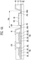
- FIG. 4A is a cross-sectional view illustrating a pixel according to one embodiment of the present invention.
- FIG. 4A shows cross sections of a first thin film transistor TR1, a second thin film transistor TR2, and a light-emitting element ED.
- a base layer BL may be a silicon substrate, a plastic substrate, a glass substrate, an insulating film, or a stacked structure including a plurality of insulating layers.
- the first thin film transistor TR1 and the second thin film transistor TR2 may be disposed on the base layer BL.
- the first thin film transistor TR1 may include a first control electrode CE1, a first input electrode IE1, a first output electrode OE1, and a first semiconductor pattern SP1.
- the second thin film transistor TR2 may include a second control electrode CE2, a second input electrode IE2, a second output electrode OE2, and a second semiconductor pattern SP2.
- the first control electrode CE1 and the second control electrode CE2 may be disposed on the base layer BL.
- the first control electrode CE1 and the second control electrode CE2 may include a conductive material.
- a first insulating layer L1 may be disposed on the base layer BL and may cover the first control electrode CE1 and the second control electrode CE2. That is, the first control electrode CE1 and the second control electrode CE2 may be disposed between the first insulating layer L1 and the base layer BL.
- the first semiconductor pattern SP1 and the second semiconductor pattern SP2 may be disposed on the first insulating layer L1.
- Each of the first and second semiconductor patterns SP1 and SP2 may include a semiconductor material.
- the first semiconductor pattern SP1 and the second semiconductor pattern SP2 may include the same semiconductor material and may also include different semiconductor materials.
- the semiconductor material may include, for example, at least one selected from amorphous silicon, polycrystalline silicon, single crystalline silicon, an oxide semiconductor, and a compound semiconductor.
- Each of the first and second semiconductor patterns SP1 and SP2 may include a channel region serving as a path through which electrons or holes are moved, and a first ion doping region and a second ion doping region which are disposed with the channel region interposed therebetween.
- the first input electrode IE1 and the first output electrode OE1 may be disposed on the first semiconductor pattern SP1, and the second input electrode IE2 and the second output electrode OE2 may be disposed on the second semiconductor pattern SP2.
- a second insulating layer L2 may be disposed on the first insulating layer L1 and may cover the first and second semiconductor patterns SP1 and SP2, the first and second input electrodes IE1 and IE2, and the first and second output electrodes OE1 and OE2. That is, the first and second semiconductor patterns SP1 and SP2, the first and second input electrodes IE1 and IE2, and the first and second output electrodes OE1 and OE2 may be disposed between the first insulating layer L1 and the second insulating layer L2.
- a third insulating layer L3 may be disposed on the second insulating layer L2.
- the first insulating layer L1 and the second insulating layer L2 may include an inorganic material
- the third insulating layer L3 may include an organic material.
- the third insulating layer L3 may provide a flat surface.
- the inorganic material may be, for example, silicon nitride, silicon oxynitride, silicon oxide, titanium oxide, or aluminium oxide, but the present invention is not limited thereto.
- a connection electrode CCE may be disposed on the third insulating layer L3.
- the connection electrode CCE may connect the first output electrode OE1 and the second control electrode CE2.
- a through-hole may be formed in the second and third insulating layers L2 and L3, and the first output electrode OE1 may be exposed by the through-hole.
- the connection electrode CCE may be electrically connected to the exposed first output electrode OE1.
- a through-hole may be formed in the first to third insulating layers L1, L2, and L3, and the second control electrode CE2 may be exposed by the through-hole.
- the connection electrode CCE may be electrically connected to the exposed second control electrode CE2.
- a first electrode E1 may be disposed on the third insulating layer L3.
- a through-hole may be formed in the second and third insulating layers L2 and L3, and the second output electrode OE2 may be exposed by the through-hole.
- the first electrode E1 may be electrically connected to the exposed second output electrode OE2.
- a second electrode E2 may be disposed on the third insulating layer L3. Although not shown, the second electrode E2 may be electrically connected to the second power line PL2 (see FIG. 3 ). That is, the second power voltage ELVSS (see FIG. 3 ) may be supplied to the second electrode E2.
- connection electrode CCE, the first electrode E1, and the second electrode E2 may include the same conductive material.
- the conductive material may include one selected from indium zinc oxide (IZO), indium tin oxide (ITO), indium gallium oxide (IGO), indium gallium zinc oxide (IGZO), and a mixture/compound thereof.
- the present invention is not limited thereto.
- the conductive material may be a metal material, and the metal material may include, for example, molybdenum, silver, titanium, copper, aluminium, or an alloy thereof.
- each of the first electrode E1 and the second electrode E2 may include a reflective material. Therefore, the first electrode E1 and the second electrode E2 may reflect light emitted from a light-emitting element ED.
- each of the first electrode E1 and the second electrode E2 may include a reflective electrode and a capping electrode covering the reflective electrode.
- the reflective electrode may have a structure in which indium tin oxide (ITO), silver (Ag), and indium tin oxide (ITO) are sequentially stacked, and the capping electrode may include indium zinc oxide (IZO) and may cover the reflective electrode.
- a groove GRV may be formed in the first to third insulating layers L1, L2, and L3.
- the first electrode E1 and the second electrode E2 may extend to be disposed in the groove GRV.
- the light-emitting element ED may be disposed on the first electrode E1 and the second electrode E2.
- the light-emitting element ED may be electrically connected to the first electrode E1 and the second electrode E2.
- a pixel emission area PXA may be defined as an area including an area corresponding to an area in which the light-emitting element ED is disposed.
- the groove GRV may be omitted, the first electrode E1 and the second electrode E2 may be disposed on the third insulating layer L3, and the light-emitting element ED may be disposed on the first electrode E1 and the second electrode E2 disposed on the third insulating layer L3.
- a first pattern portion PT1 may be disposed in an area adjacent to an area in which the first electrode E1 and the light-emitting element ED overlap each other in a plan view
- a second pattern portion PT2 may be disposed in an area adjacent to an area in which the second electrode E2 and the light-emitting element ED overlap each other in a plan view.
- the term "in a plan view” may refer to when a display panel DP is viewed in a thickness direction thereof, that is, in the third direction DR3 (see FIG. 1 ).
- Detailed descriptions of the first pattern portion PT1 and the second pattern portion PT2 will be given below.
- a first connection electrode CNE1 may be disposed on the first pattern portion PT1, and the first connection electrode CNE1 may electrically connect the light-emitting element ED and the first electrode E1.
- a second connection electrode CNE2 may be disposed on the second pattern portion PT2, and the second connection electrode CNE2 may electrically connect the light-emitting element ED and the second electrode E2.
- the first connection electrode CNE1 and the second connection electrode CNE2 may include the same conductive material.
- the conductive material may include one selected from indium zinc oxide (IZO), indium tin oxide (ITO), indium gallium oxide (IGO), indium gallium zinc oxide (IGZO), and a mixture/compound thereof.
- the present invention is not limited thereto.
- the conductive material may be a metal material, and the metal material may include, for example, molybdenum, silver, titanium, copper, aluminium, or alloys thereof.
- a protection portion OPL may be disposed on the light-emitting element ED.
- the protection portion OPL may cover at least a portion of the light-emitting element ED to protect the light-emitting element ED.
- the protection portion OPL may include the same material as the first pattern portion PT1 and the second pattern portion PT2, and the protection portion OPL, the first pattern portion PT1, and the second pattern portion PT2 may be simultaneously formed through the same process.
- the first pattern portion PT1, the second pattern portion PT2, and the protection portion OPL may include an organic material.
- a cover layer not shown
- a polarization-functional layer not shown
- a wavelength conversion layer not shown
- a color filter not shown
- FIG. 4B is a cross-sectional view illustrating a pixel according to one embodiment of the present invention.
- a buffer layer BFL may be disposed on a base layer BL.
- Each of a first thin film transistor TR1a and a second thin film transistor TR2a may be disposed on the buffer layer BFL.
- the first thin film transistor TR1a may include a first control electrode CE1a, a first input electrode IE1a, a first output electrode OE1a, and a first semiconductor pattern SP1a.
- the second thin film transistor TR2a may include a second control electrode CE2a, a second input electrode IE2a, a second output electrode OE2a, and a second semiconductor pattern SP2a.
- the first semiconductor pattern SP1a and the second semiconductor pattern SP2a may be disposed on the buffer layer BFL.
- the buffer layer BFL may provide modified surfaces to the first semiconductor pattern SP1a and the second semiconductor pattern SP2a.
- the first semiconductor pattern SP1a and the second semiconductor pattern SP2a may have higher adhesion with respect to the buffer layer BFL as compared with when the first semiconductor pattern SP1a and the second semiconductor pattern SP2a are formed directly on the base layer BL.
- the buffer layer BFL may be a barrier layer which protects a lower surface of each of the first semiconductor pattern SP1a and the second semiconductor pattern SP2a.
- the buffer layer BFL may block contamination or moisture introduced into the base layer BL itself or through the base layer BL from permeating into the first semiconductor pattern SP1a and the second semiconductor pattern SP2a.
- a first insulating layer L1a may be disposed on the buffer layer BFL and may cover the first semiconductor pattern SP1a and the second semiconductor pattern SP2a.
- the first insulating layer L1a may include an inorganic material.
- the first control electrode CE1a and the second control electrode CE2a may be disposed on the first insulating layer L1a.
- a second insulating layer L2a may be disposed on the first insulating layer L1a and may cover the first control electrode CE1a and the second control electrode CE2a.
- the second insulating layer L2a may include an inorganic material. At least some of signal lines, for example, scan lines or data lines, may be disposed on the second insulating layer L2a.
- a third insulating layer L3a may be disposed on the second insulating layer L2a and may cover at least some of the signal lines.
- the first input electrode IE1a, the first output electrode OE1a, the second input electrode IE2a, and the second output electrode OE2a may be disposed on the third insulating layer L3a.
- the first input electrode IE1a and the first output electrode OE1a may be connected to the first semiconductor pattern SP1a through through-holes passing through the first to third insulating layers L1a, L2a, and L3a.
- the second input electrode IE2a and the second output electrode OE2a may be connected to the second semiconductor pattern SP2a through through-holes passing through the first to third insulating layers L1a, L2a, and L3a.
- a fourth insulating layer L4a may be disposed on the third insulating layer L3a and may cover the first input electrode IE1a, the first output electrode OE1a, the second input electrode IE2a, and the second output electrode OE2a.
- the fourth insulating layer L4a may be provided as a single layer or a plurality of layers, and the fourth insulating layer L4a may include an organic material and/or an inorganic material.
- a first partition wall BR1 and a second partition wall BR2 may be disposed on the fourth insulating layer L4a.
- the first partition wall BR1 and the second partition wall BR2 may be disposed to be spaced apart from each other.
- a first electrode E1a may cover the first partition wall BR1 and may be disposed on the fourth insulating layer L4a.
- a through-hole may be formed in the fourth insulating layer L4a, and the second output electrode OE2a may be exposed by the through-hole.
- the first electrode E1a may be electrically connected to the exposed second output electrode OE2a.
- a second electrode E2a may cover the second partition wall BR2 and may be disposed on the fourth insulating layer L4a. Although not shown, the second electrode E2a may be electrically connected to the second power line PL2 (see FIG. 3 ). That is, the second power voltage ELVSS (see FIG. 3 ) may be supplied to the second electrode E2a.
- a light-emitting element ED may be disposed on the first electrode E1a and the second electrode E2a.
- the light-emitting element ED may be electrically connected to the first electrode E1a and the second electrode E2a.
- FIG. 4B shows an example in which the light-emitting element ED is disposed on the fourth insulating layer L4a, but the present invention is not limited thereto.
- a groove (not shown) may be provided in the first to fourth insulating layers L1a, L2a, L3a, and L4a.
- the shape of the groove may be similar to that shown in FIG. 4A .
- the first electrode E1a and the second electrode E2a may extend to be disposed on the buffer layer BFL exposed by the groove, and the light-emitting element ED may be disposed on the extending first and second electrodes E1a and E2a.
- FIG. 5A is a cross-sectional view of a light-emitting element according to one embodiment of the present invention.
- a light-emitting element ED may have various shapes such as a cylindrical shape and a polygonal column shape.
- the light-emitting element ED may include an N-type semiconductor layer SCN, a P-type semiconductor layer SCP, and an active layer AL.
- the active layer AL may be disposed between the N-type semiconductor layer SCN and the P-type semiconductor layer SCP.
- the N-type semiconductor layer SCN may be provided by an N-type dopant being doped into a semiconductor layer
- the P-type semiconductor layer SCP may be provided by a P-type dopant being doped into a semiconductor layer.
- the semiconductor layer may include a semiconductor material, and the semiconductor material may be, for example, GaN, A1N, AlGaN, InGaN, InN, InAlGaN, or AlInN, but is not limited thereto.
- the N-type dopant may be silicon (Si), germanium (Ge), tin (Sn), selenium (Se), tellurium (Te), or a combination thereof, but is not limited thereto.
- the P-type dopant may be magnesium (Mg), zinc (Zn), calcium (Ca), strontium (Sr), barium (Ba), or a combination thereof, but is not limited thereto.
- the active layer AL may be formed to have at least one of a single-quantum well structure, a multi-quantum well structure, a quantum wire structure, and a quantum dot structure.
- the active layer AL may be a region in which electrons injected through the N-type semiconductor layer SCN and holes injected through the P-type semiconductor layer SCP recombine.
- the active layer AL is a layer which emits light having energy determined by an intrinsic energy band of a material.
- the position of the active layer AL may be variously changed according to a type of diode.
- a length LT of the light-emitting element ED may be in a range of several nanometers to several hundred micrometers.
- the length LT of the light-emitting element ED may be in a range of 1 micrometer to 100 micrometers.
- FIG. 5B is a cross-sectional view of a light-emitting element according to one embodiment of the present invention.
- a light-emitting element EDa may further include a first electrode layer ECL1 and a second electrode layer ECL2.
- the first electrode layer ECL1 may be adjacent to an N-type semiconductor layer SCN, and the second electrode layer ECL2 may be adjacent to a P-type semiconductor layer SCP.
- the first electrode layer ECL1, the N-type semiconductor layer SCN, an active layer AL, the P-type semiconductor layer SCP, and the second electrode layer ECL2 may be sequentially stacked.
- Each of the first electrode layer ECL1 and the second electrode layer ECL2 may be made of a metal or an alloy of metals.
- each of the first electrode layer ECL1 and the second electrode layer ECL2 may be made of at least one metal selected from molybdenum (Mo), chromium (Cr), nickel (Ni), gold (Au), aluminium (Al), titanium (Ti), platinum (Pt), vanadium (V), tungsten (W), lead (Pd), copper (Cu), rhodium (Rh), and iridium (Ir) or may be made of an alloy of the metals.
- the first electrode layer ECL1 and the second electrode layer ECL2 may include the same material or may also include different materials.
- FIG. 5C is a cross-sectional view of a light-emitting element according to one embodiment of the present invention.
- a light-emitting element EDb may further include an insulating film IL.
- the light-emitting element EDb may have a core-shell structure.
- the insulating film IL may cover an N-type semiconductor layer SCN, a P-type semiconductor layer SCP, and an active layer AL to protect outer surfaces of the N-type semiconductor layer SCN, the P-type semiconductor layer SCP, and the active layer AL.
- the insulating film IL may also cover only the active layer AL.
- FIG. 5D is a cross-sectional view of a light-emitting element according to one embodiment of the present invention.
- a light-emitting element EDc may further include an insulating film ILa.
- the insulating film ILa may cover an N-type semiconductor layer SCN, a P-type semiconductor layer SCP, and an active layer AL and may not cover a first electrode layer ECL1 and a second electrode layer ECL2. However, in another embodiment of the present invention, the insulating film ILa may cover at least some of the first electrode layer ECL1 and the second electrode layer ECL2 or may cover both the first electrode layer ECL1 and the second electrode layer ECL2.
- FIG. 6 is a plan view of a pixel according to one embodiment of the present invention. Specifically, FIG. 6 may be a plan view of a portion corresponding to a pixel emission area PXA.
- a first electrode E1 and a second electrode E2 may be disposed to be spaced apart from each other.
- One portion of a light-emitting element ED may be in contact with the first electrode E1, and the other portion of the light-emitting element ED may be in contact with the second electrode E2.
- an area, in which the light-emitting element ED and the first electrode E1 overlap each other is defined as a first area AR1
- an area, in which the light-emitting element ED and the second electrode E2 overlap each other is defined as a second area AR2.
- a first pattern portion PT1 may be disposed adjacent to the first area AR1, and a second pattern portion PT2 may be disposed adjacent to the second area AR2.
- the first pattern portion PT1 may surround at least a portion of the first area AR1, and the second pattern portion PT2 may surround at least a portion of the second area AR2.
- the first pattern portion PT1 may surround one end portion of the light-emitting element ED, and the second pattern portion PT2 may surround the other end portion of the light-emitting element ED.
- the first pattern portion PT1 and the second pattern portion PT2 may include an organic material.
- a plurality of light-emitting elements ED may be provided in one pixel emission area PXA.
- the plurality of light-emitting elements ED may be connected to each other in parallel.
- only a single light-emitting element ED may be provided in one pixel emission area PXA.
- a first connection electrode CNE1 may cover one end portions of the plurality of light-emitting elements ED in a plan view.
- a second connection electrode CNE2 may cover the other end portions of the plurality of light-emitting elements ED in a plan view.
- the first connection electrode CNE1 may be provided to overlap the first electrode E1
- the second connection electrode CNE2 may be provided to overlap the second electrode E2. That is, the first connection electrode CNE1 may electrically connect one end portions of the plurality of light-emitting elements ED and the first electrode E1
- the second connection electrode CNE2 may electrically connect the other ends of the plurality of light-emitting elements ED and the second electrode E2.
- a protection portion OPL may be disposed between the first electrode E1 and the second electrode E2.
- the protection portion OPL may cover the plurality of light-emitting elements ED disposed in the pixel emission area PXA.
- the protection portion OPL may serve to protect the plurality of light-emitting elements ED, and the protection portion OPL may include an organic material.
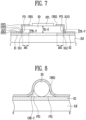
- FIG. 7 is an example of a cross-sectional view taken along line I-I' shown in FIG. 6
- FIG. 8 is an example of a cross-sectional view taken along line II-II' shown in FIG. 6 .
- a first electrode E1 and a second electrode E2 are disposed on a base insulating layer ILB.
- the base insulating layer ILB may be the base layer BL described with reference to FIG. 4A or the fourth insulating layer L4a described with reference to FIG. 4B .
- a light-emitting element ED is disposed on the first electrode E1 and the second electrode E2.
- a first pattern portion PT1 may be disposed on the first electrode E1, and a second pattern portion PT2 may be disposed on the second electrode E2.
- the light-emitting element ED may have a cylindrical shape. Accordingly, the light-emitting element ED may have a circular shape in a cross section shown in FIG. 8 .
- the first pattern portion PT1 may have a first inclined surface SLP1, and the second pattern portion PT2 may have a second inclined surface SLP2.
- FIG. 7 shows the first inclined surface SLP1 connecting a point having a maximum height in the first pattern portion PT1 and an end portion of the first pattern portion PT1.
- the first inclined surface SLP1 may have a plurality of gradients.
- a first inclined surface SLP1 may have curvature.
- the end portion of the first pattern portion PT1 may mean an end portion of the first pattern portion PT1, at which the first inclined surface SLP1 and the first electrode E1 are in contact with each other.
- the second inclined surface SLP2 of the second pattern portion PT2 may also have a plurality of gradients.
- a first connection electrode CNE1 may be disposed on the light-emitting element ED, the first electrode E1, and the first pattern portion PT1, and a second connection electrode CNE2 may be disposed on the light-emitting element ED, the second electrode E2, and the second pattern portion PT2.
- the first connection electrode CNE1 may be in contact with the first inclined surface SLP1, and the second connection electrode CNE2 may be in contact with the second inclined surface SLP2.
- a first portion POT1 covering a portion of an upper surface of the light-emitting element ED and a portion of a side surface of the light-emitting element ED, and a second portion POT2 covering the second pattern portion PT2, and a third portion POT3 covering a portion of the second electrode E2 1 may be defined.
- the first portion POT1 may be in contact with the light-emitting element ED
- the second portion POT2 may be in contact with the second inclined surface SLP2
- the third portion POT3 may be in contact with the second electrode E2.
- a comparative connection electrode CNE-C may be formed along an outer surface of the light-emitting element ED.
- the comparative connection electrode CNE-C is shown by a dotted line in FIG. 8 .
- a portion between a contact portion of the comparative connection electrode CNE-C and the second electrode E2 and a contact portion of the comparative connection electrode CNE-C and the light-emitting element ED may have a bent shape.
- an angle between a contact portion of the comparative connection electrode CNE-C and the light-emitting element ED and a contact portion of the comparison connection electrode CNE-C and the first electrode E1 may be close to 90°.
- the comparison connection electrode CNE-C may be disconnected to not connect the first electrode E1 and the light-emitting element ED, or cracks may be generated in the comparison connection electrode CNE-C to increase resistance of the comparative connection electrode CNE-C.
- the comparative connection electrode CNE-C is disconnected, the light-emitting element ED may not emit light, and when cracks are generated in the comparative connection electrode CNE-C, luminous efficiency of the light-emitting element ED may be lowered.
- a process time of an etching process of patterning the comparative connection electrode CNE-C may be increased, and as the process time may be increased, etch skew may occur.
- pattern uniformity is lowered due to the etch skew, characteristics of an element may be changed.
- a pattern may be disconnected due to the etch skew.
- the first pattern portion PT1 is disposed between the first connection electrode CNE1 and the light-emitting element ED.
- a change in gradient of the first connection electrode CNE1 may be relatively gradual due to the first pattern portion PT1. Therefore, it is possible to reduce a phenomenon in which the first connection electrode CNE1 is disconnected or cracked due to an abrupt change in gradient. Therefore, the first connection electrode CNE1 may be formed to be thinner than the comparative connection electrode CNE-C.
- a process time of an etching process of patterning the first connection electrode CNE1 may also be reduced. As the process time of the etching process is reduced, the probability of etch skew may also be reduced, which may be advantageous in forming a fine pattern.
- the second pattern portion PT2 has substantially the same shape as the first pattern portion PT1, descriptions of the second pattern portion PT2 are omitted.
- a change in gradient being gradual means that a difference between a first gradient and a second gradient different from each other is reduced.
- a maximum height TK-P of each of the first pattern portion PT1 and the second pattern portion PT2 may be smaller than a thickness TK-E of the light-emitting element ED.
- the maximum height TK-P may correspond to a height of a portion at which each of the first pattern portion PT1 and the second pattern portion PT2 is in contact with the light-emitting element ED.
- the maximum height TK-P of each of the first pattern portion PT1 and the second pattern portion PT2 may be 50% or less of the thickness TK-E of the light-emitting element ED.
- the maximum height TK-P may be in a range of 1% to 50% of the thickness TK-E of the light-emitting element ED.
- An angle DG1 between the first inclined surface SLP1 and the first electrode E1 and an angle DG2 between the second inclined surface SLP2 and the second electrode E2 may be 70° or less.
- a gradient between the second portion POT2 and the third portion POT3 of each of the first connection electrode CNE1 and the second connection electrode CNE2 may be abruptly changed.
- the abrupt change in gradient may cause cracks or disconnection of the first connection electrode CNE1 and the second connection electrode CNE2.
- the angles DG1 and DG2 may be in a range of 1° to 70°.
- a phenomenon, in which the first and second connection electrodes CNE1 and CNE2 are disconnected or cracked, may be prevented due to the first and second pattern portions PT1 and PT2.
- product manufacturing yield may be improved, and the light-emitting element ED may be stably coupled to the first electrode E1 and the second electrode E2, thereby improving product reliability.
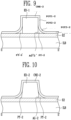
- FIG. 9 is an example of a cross-sectional view taken along line II-II' of FIG. 6 .
- a light-emitting element ED-1 may have a polygonal column shape.
- the light-emitting element ED-1 may have a rectangular column shape.
- An angle AG-1 formed between one side of the light-emitting element ED-1 and a second electrode E2 may be 90°.
- a pattern portion PT-2 is provided between the light-emitting element ED-1 and a connection electrode CNE-2.
- a portion at which a gradient of the connection electrode CNE-2 1 is abruptly changed may be removed due to the pattern portion PT-2.
- the gradient of the connection electrode CNE-2 1 may be directly changed from a gradient of a first portion POT1-2 to a gradient of a third portion POT3-2.
- the gradient of the connection electrode CNE-2 may be changed from the gradient of the first portion POT1-2 to a gradient of a second portion POT2-2 1 and then may be changed to the gradient of the third portion POT3-2.
- FIG. 10 is an example of a cross-sectional view taken along line II-II' shown in FIG. 6 .
- a light-emitting element ED-2 may have a polygonal column shape.
- the light-emitting element ED-2 may have a trapezoidal column shape.
- An angle AG-2 formed between one side of the light-emitting element ED-2 and a second electrode E2 may be 70°.
- a pattern portion PT-2 may be applied.
- a gradient of a connection electrode CNE-2 may be abruptly changed. Therefore, a change in gradient of the connection electrode CNE-2 may be gradual by applying the pattern portion PT-2.
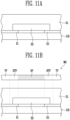
- FIGS. 11A to 11H are views illustrating some of the processes of manufacturing a display device according to one embodiment of the present invention.
- a first electrode E1 and a second electrode E2 are formed on a base insulating layer ILB.
- a light-emitting element ED is disposed or transferred onto the first electrode E1 and the second electrode E2.
- a plurality of light-emitting elements ED may be provided, the plurality of light-emitting elements ED may be simultaneously transferred, or a single light-emitting element ED may be transferred one by one.
- a method of transferring the light-emitting element ED onto the first electrode E1 and the second electrode E2 may include a direct transfer method and a printing transfer method.
- the direct transfer method may be a method of directly transferring the light-emitting element ED to the first electrode E1 and the second electrode E2.
- the printing transfer method may be a method of transferring the light-emitting element ED to the first electrode E1 and the second electrode E2 using an electrostatic head, a flat stamp, or a roll stamp.
- a solvent such as an ink or a paste containing the light-emitting element ED may be supplied onto the first electrode E1 and the second electrode E2 to transfer the light-emitting element ED.
- the solvent may be a material that may be vaporized at room temperature or by heat.
- Power is applied to the first electrode E1 and the second electrode E2 to form an electric field between the first electrode E1 and the second electrode E2.
- Bipolarity may be induced in the light-emitting element ED by the electric field, and the light-emitting element ED may be aligned on the first electrode E1 and the second electrode E2 by a dielectrophoretic force.
- An organic layer OL covering the light-emitting element ED, the first electrode E1, and the second electrode E2 is formed.
- the organic layer OL may be formed through a coating process, and a process of forming the organic layer OL is not limited thereto.
- the organic layer OL may be a photoresist layer.
- a mask MK is disposed on the organic layer OL.
- the mask MK may be a halftone mask including a half-transparent portion HTP, a transparent portion TP, and a light-blocking portion BP.
- the organic layer OL may be a positive photoresist layer or a negative photoresist layer.
- FIG. 11B a case in which the organic layer OL is a positive photoresist layer is described as an example.
- At least a portion of the half-transparent portion HTP may overlap the first electrode E1 and the second electrode E2 in a plan view.
- the light-blocking portion BP may be disposed to overlap a portion of the light-emitting element ED, which does not overlap the first electrode E1 and the second electrode E2.
- the transparent portion TP may be disposed in other areas. After the mask MK is disposed on the organic layer OL, light is irradiated.
- the exposed organic layer OL (see FIG. 11B ) is developed to form an organic pattern OP.
- the organic pattern OP may include a first organic pattern portion OP1 and a second organic pattern portion OP2.
- the first organic pattern portion OP1 may be a portion which remains due to light being blocked
- the second organic pattern portion OP2 may be a portion in which a portion of the organic layer OL (see FIG. 11B ) in a thickness direction thereof is removed due to light being partially irradiated.
- the organic pattern OP is formed and then is baked.
- a thickness TKx of a portion of the second organic pattern portion OP2, which is disposed on the light-emitting element ED, may be different from a thickness TKy of a portion of the second organic pattern portion OP2, which is disposed on the first electrode E1 and the second electrode E2.
- a thickness difference of the second organic pattern portion OP2 may be generated due to a stepped portion formed by the light-emitting element ED.
- FIGS. 11D and 11E an operation of removing a portion of the organic pattern OP is shown.
- FIG. 11D shows a state in which a portion of the organic pattern OP (see FIG. 11C ) is being removed
- FIG. 11E shows a state in which a portion of the organic pattern OP is completely removed.
- a portion of the organic pattern OP may be removed using an ashing process.
- the thickness of a first organic pattern portion OP1-s and the thickness of a second organic pattern portion OP2-s may be gradually reduced.
- a portion of the second organic pattern portion OP2-s may remain without being removed due to a difference in thickness for each area thereof.
- the remaining portion may constitute a first pattern portion PT1 and a second pattern portion PT2.
- the thickness of the first organic pattern portion OP1-s may be reduced to constitute a protection portion OPL.
- the first pattern portion PT1, the second pattern portion PT2, and the protection portion OLP may be simultaneously formed through the same process.
- FIG. 11F is a plan view of FIG. 11E .
- the first pattern portion PT1 may remain by surrounding one end portion of the light-emitting element ED, and the second pattern portion PT2 may remain by surrounding the other end portion of the light-emitting element ED.
- the protection portion OPL may cover at least a portion of an upper surface of the light-emitting element ED.
- the protection portion OPL may serve to prevent an array of the light-emitting elements ED from being distorted, and the protection portion OPL may also serve to protect the light-emitting elements ED during a subsequent process.
- the conductive layer MTL may include one selected from indium zinc oxide (IZO), indium tin oxide (ITO), indium gallium oxide (IGO), indium gallium zinc oxide (IGZO), and a mixture/compound thereof.
- IZO indium zinc oxide
- ITO indium tin oxide
- IGO indium gallium oxide
- IGZO indium gallium zinc oxide
- the present invention is not limited thereto.
- the conductive layer MTL may include molybdenum, silver, titanium, copper, aluminium, or an alloy thereof.
- the conductive layer MTL is patterned to form a first connection electrode CNE1 and a second connection electrode CNE2.
- changes in gradients of the first connection electrode CNE1 and the second connection electrode CNE2 may be gradual due to the first pattern portion PT1 and the second pattern portion PT2. Therefore, it is possible to reduce a phenomenon in which the first connection electrode CNE1 and the second connection electrode CNE2 are disconnected or cracked. Since the possibility of occurrence of disconnection or cracks is reduced, the thicknesses of the first connection electrode CNE1 and the second connection electrode CNE2 may be reduced. Thus, a process time of an etching process may be reduced, which may be advantageous for a fine pattern manufacturing process.
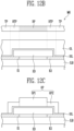
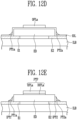
- FIGS. 12A to 12G are views illustrating some of the processes of manufacturing a display device according to one embodiment of the present invention.
- FIGS. 12A to 12G portions different from those in FIGS. 11A to 11F will be described in detail, and the same reference numerals will be used for the same components, and descriptions of the same components will be omitted.
- an inorganic layer IOL covering a light-emitting element ED, a first electrode E1, and a second electrode E2 is formed, and after the inorganic layer IOL is formed, an organic layer OL is formed.
- a mask MK is disposed on the organic layer OL, and light is irradiated onto the organic layer OL.
- the exposed organic layer OL is developed to form an organic pattern OP.
- the organic pattern OP may be disposed on the inorganic layer IOL.
- the organic pattern OP is ashed to form an organic protection portion OPLa, a first pattern portion PT1a, and a second pattern portion PT2a.
- the organic protection portion OPLa may be referred to as a second protection portion.
- a portion of the inorganic layer IOL (see FIG. 12D ) not covered by the organic protection portion OPLa, the first pattern portion PT1a, and the second pattern portion PT2a is removed.
- a portion of the inorganic layer IOL may be removed to form a first inorganic pattern portion IPT1, a second inorganic pattern portion IPT2, and an inorganic protection portion IOPLa. That is, the first inorganic pattern portion IPT1, the second inorganic pattern portion IPT2, and the inorganic protection portion IOPLa may be simultaneously formed through the same process.
- the inorganic protection portion IOPLa may be referred to as a first protection portion.
- the protection portion PTP may include a first protection portion IOPLa including an inorganic material and a second protection portion OPLa.
- the first inorganic pattern portion IPT1 may be disposed under the first pattern portion PT1a, and the second inorganic pattern portion IPT2 may be disposed under the second pattern portion PT2a.
- the first inorganic pattern portion IPT1 may be disposed between the first pattern portion PT1a and the light-emitting element ED and between the first pattern portion PT1a and the first electrode E1
- the second inorganic pattern portion IPT2 may be disposed between the second pattern portion PT2a and the light-emitting element ED and between the second pattern portion PT2a and the second electrode E2.
- a conductive layer MTL is formed.
- the conductive layer MTL may cover all of the first electrode E1, the second electrode E2, the first pattern portion PT1a, the second pattern portion PT2a, the first inorganic pattern portion IPT1, the second inorganic pattern portion IPT2, the first protection portion IOPLa, and the second protection portion OPLa.
- the conductive layer MTL is patterned to form a first connection electrode CNE1 and a second connection electrode CNE2.
- the first connection electrode CNE1 may electrically connect the light-emitting element ED and the first electrode E1
- the second connection electrode CNE2 may electrically connect the light-emitting element ED and the second electrode E2.
- the present invention is not limited thereto.
- the conductive layer MTL is patterned to form the first connection electrode CNE1, and an insulating layer (not shown) covering the first connection electrode CNE1 is formed. Thereafter, the conductive layer may be formed on the insulating layer, and the conductive layer may be patterned to form the second connection electrode CNE2. That is, the first connection electrode CNE1 and the second connection electrode CNE2 may not be simultaneously formed.
- changes in gradients of the first connection electrode CNE1 and the second connection electrode CNE2 may be gradual due to the first pattern portion PT1a and the second pattern portion PT2a. Accordingly, it is possible to reduce a phenomenon in which each of the first connection electrode CNE1 and the second connection electrode CNE2 is disconnected or cracked. In addition, since the possibility of occurrence of disconnection or cracks is reduced, the thicknesses of the first connection electrode CNE1 and the second connection electrode CNE2 may be reduced. Thus, a process time of an etching process may be reduced, which may be advantageous for a fine pattern manufacturing process.
- the present invention provides a display device having improved connection stability between a light-emitting element and an electrode, and a method for manufacturing the display device. Therefore, the display device and the present invention relating to the display device have high industrial applicability.
Landscapes
- Electroluminescent Light Sources (AREA)
- Devices For Indicating Variable Information By Combining Individual Elements (AREA)
Claims (15)
- Anzeigevorrichtung (DD), Folgendes umfassend:eine erste Elektrode (E1);eine zweite Elektrode (E2), die von der ersten Elektrode (E1) beabstandet ist;ein lichtemittierendes Element (ED, ED-1, ED-2), das direkt auf der ersten Elektrode (E1) und der zweiten Elektrode (E2) angeordnet ist;einen ersten Strukturabschnitt (PT1, PT1a), der auf der ersten Elektrode (E1) und angrenzend an eine erste Fläche (AR1) angeordnet ist, in der die erste Elektrode (E1) und das lichtemittierende Element (ED, ED-1, ED-2) einander in einer Draufsicht überlappen;einen zweiten Strukturabschnitt (PT2, PT2a), der auf der zweiten Elektrode (E2) und angrenzend an eine zweite Fläche (AR2) angeordnet ist, in der die zweite Elektrode (E2) und das lichtemittierende Element (ED, ED-1, ED-2) einander in einer Draufsicht überlappen;eine erste Verbindungselektrode (CNE1), die das lichtemittierende Element (ED) und den ersten Strukturabschnitt (PT1, PT1a) abdeckt und mit dem lichtemittierenden Element (ED) und der ersten Elektrode (E1) elektrisch verbunden ist; undeine zweite Verbindungselektrode (CNE2), die das lichtemittierende Element (E2) und den zweiten Strukturabschnitt (PT2, PT2a) bedeckt und elektrisch mit dem lichtemittierenden Element (ED, ED-1, ED-2) und der zweiten Elektrode (E2) verbunden ist.
- Anzeigevorrichtung (DD) nach Anspruch 1, wobei jeder des ersten Strukturabschnitts (PT1, PT1a) und des zweiten Strukturabschnitts (PT2, PT2a) ein organisches Material einschließt.
- Anzeigevorrichtung (DD) nach Anspruch 1 oder Anspruch 2, wobei eine Vielzahl von lichtemittierenden Elementen (ED, ED-1, ED-2), die mit dem lichtemittierenden Element (ED, ED-1, ED-2) identisch sind, bereitgestellt werden und parallel verbunden sind.
- Anzeigevorrichtung (DD) nach einem der Ansprüche 1 bis 3, wobei eine erste Dicke (TK-E) des lichtemittierenden Elements (ED, ED-1, ED-2) größer ist als eine erste maximale Höhe (TK-P) des ersten Strukturabschnitts (PT1, PT1a) und eine zweite maximale Höhe (TK-P) des zweiten Strukturabschnitts (PT2, PT2a), wobei optional jede der ersten maximalen Höhe (TK-P) und der zweiten maximalen Höhe (TK-P) 50 % oder weniger der ersten Dicke (TK-E) beträgt.
- Anzeigevorrichtung (DD) nach einem der Ansprüche 1 bis 4, wobei ein Neigungswinkel (AG-2) zwischen der ersten Elektrode (E1) und dem lichtemittierenden Element 60° oder mehr beträgt.
- Anzeigevorrichtung (DD) nach einem der Ansprüche 1 bis 5, wobei ein erster Abschnitt (POT1), der auf dem lichtemittierenden Element (ED, ED-1, ED-2) angeordnet ist, ein zweiter Abschnitt (POT2), der auf dem ersten Strukturabschnitt (PT1, PT1a) angeordnet ist, und ein dritter Abschnitt (POT3), der auf der ersten Elektrode (E1) angeordnet ist, in der ersten Verbindungselektrode (CNE1) definiert sind; und
ein Winkel (DG1) zwischen einer schrägen Oberfläche (SLP1) des ersten Strukturabschnitts (PT1, PT1a) in Kontakt mit dem zweiten Abschnitt (POT2) und der ersten Elektrode (E1), die unter dem ersten Strukturabschnitt angeordnet ist, 70° oder weniger beträgt. - Anzeigevorrichtung (DD) nach einem der Ansprüche 1 bis 6, ferner einen Schutzabschnitt (OPL, PTP), der auf dem lichtemittierenden Element (ED) angeordnet ist, umfassend,
wobei der Schutzabschnitt (OPL, PTP) zwischen dem ersten Strukturabschnitt (PT1, PT1a) und dem zweiten Strukturabschnitt (PT2, PT2a) in einer Draufsicht angeordnet ist, wobei optional:der Schutzabschnitt (PTP) einen ersten Schutzabschnitt (IOPLa), der ein anorganisches Material einschließt, und einen zweiten Schutzabschnitt (OPLa), der ein organisches Material einschließt, einschließt, undder erste Schutzabschnitt (IOPLa) zwischen dem zweiten Schutzabschnitt (OPLa) und dem lichtemittierenden Element (ED, ED-1, ED-2) angeordnet ist. - Anzeigevorrichtung (DD) nach einem der Ansprüche 1 bis 7, wobei:(i) die Anzeigevorrichtung (DD) ferner Folgendes umfasst:einen ersten anorganischen Strukturabschnitt (IPT1), der zwischen dem ersten Strukturabschnitt (PT1a) und dem lichtemittierenden Element (ED, ED-1, ED-2) und zwischen dem ersten Strukturabschnitt (PT1a) und der ersten Elektrode (E1) angeordnet ist, undeinen zweiten anorganischen Strukturabschnitt (IPT2), der zwischen dem zweiten Strukturabschnitt (PT2a) und dem lichtemittierenden Element (ED, ED-1, ED-2) und zwischen dem zweiten Strukturabschnitt (PT2a) und der zweiten Elektrode (E2) angeordnet ist; und/oder(ii) das lichtemittierende Element (ED, ED-1, ED-2) eine zylindrische Form oder eine polygonale Säulenform aufweist.
- Anzeigevorrichtung (DD) nach Anspruch 1, wobei:die erste Verbindungselektrode (CNE1) auf der ersten Elektrode (E1) angeordnet ist;die zweite Verbindungselektrode (CNE2) auf der zweiten Elektrode (E2) angeordnet ist;der erste Strukturabschnitt (PT1, PT1a) zwischen der ersten Verbindungselektrode (CNE1) und dem lichtemittierenden Element (ED, ED-1, ED-2) und zwischen der ersten Verbindungselektrode (CNE1) und der ersten Elektrode (E1) angeordnet ist und eine erste schräge Oberfläche (SLP1) in Kontakt mit der ersten Verbindungselektrode (CNE1) aufweist; undder zweite Strukturabschnitt (PT2, PT2a) zwischen der zweiten Verbindungselektrode (CNE2) und dem lichtemittierenden Element (ED, ED-1, ED-2) und zwischen der zweiten Verbindungselektrode (CNE2) und der zweiten Elektrode (E2) angeordnet ist und eine zweite schräge Oberfläche (SPL2) in Kontakt mit der zweiten Verbindungselektrode (CNE2) aufweist, wobei optional jeder von dem ersten Strukturabschnitt (PT1, PT1a) und dem zweiten Strukturabschnitt (PT2, PT2a) ein organisches Material einschließt.
- Anzeigevorrichtung (DD) nach Anspruch 9, wobei:(i) der erste Strukturabschnitt (PT1, PT1a) mindestens einen Abschnitt einer Fläche (AR1) umgibt, in der das lichtemittierende Element (ED, ED-1, ED-2) und die erste Elektrode (E1) einander in einer Draufsicht überlappen, und
der zweite Strukturabschnitt (PT2, PT2a) mindestens einen Abschnitt einer Fläche (AR2) umgibt, in der das lichtemittierende Element (ED, ED-1, ED-2) und die zweite Elektrode (E2) einander in einer Draufsicht überlappen; und/oder(ii) jeder von einem Winkel (DG1) zwischen der ersten schrägen Oberfläche (SLP1) und der ersten Elektrode (E1) und einem Winkel (DG2) zwischen der zweiten schrägen Oberfläche (SLP2) und der zweiten Elektrode (E2) 70° oder weniger beträgt. - Verfahren zur Herstellung einer Anzeigevorrichtung (DD), wobei das Verfahren Folgendes umfasst:Bilden einer ersten Elektrode (E1) und einer zweiten Elektrode (E2) auf einer Isolierschicht (ILB);Anordnen eines lichtemittierenden Elements (ED, ED-1, ED-2) direkt auf der ersten Elektrode (E1) und der zweiten Elektrode (E2);Bilden einer organischen Schicht (OL), die das lichtemittierende Element (ED, ED-1, ED-2), die erste Elektrode (E1) und die zweite Elektrode (E2) bedeckt;Anordnen einer Maske (MK) auf der organischen Schicht (OL);Bilden einer organischen Struktur (OP) durch Belichten und Entwickeln der organischen Schicht (OL) unter Verwendung der Maske (MK);Entfernen eines Abschnitts der organischen Struktur (OP), um einen ersten Strukturabschnitt (PT1, PT1a) zu bilden, der auf der ersten Elektrode und angrenzend an eine erste Fläche (AR1) angeordnet ist, in der die erste Elektrode (E1) und das lichtemittierende Element (ED, ED-1, ED-2) einander in einer Draufsicht überlappen und einen zweiten Strukturabschnitt (PT2) bilden, der auf der zweiten Elektrode angeordnet ist und an eine zweite Fläche (AR2) angrenzt, in der die zweite Elektrode (E2) und das lichtemittierende Element (ED, ED-1, ED-2) einander in einer Draufsicht überlappen; undBilden einer ersten Verbindungselektrode (CNE1), die elektrisch mit dem lichtemittierenden Element (ED, ED-1, ED-2) und der ersten Elektrode (E1) auf dem ersten Strukturabschnitt (PT1, PT1a) verbunden ist, und einer zweiten Verbindungselektrode (CNE2), die elektrisch mit dem lichtemittierenden Element (ED, ED-1, ED-2) und der zweiten Elektrode (E2) auf dem zweiten Strukturabschnitt (PT2) verbunden ist.
- Verfahren nach Anspruch 11, wobei die Maske (MK) eine Halbtonmaske ist, die einen halbtransparenten Abschnitt (HTP) einschließt, und
die Maske (MK) so angeordnet ist, dass der halbtransparente Abschnitt (HTP) in einer Fläche angeordnet ist, welche die erste Elektrode (E1) und die zweite Elektrode (E2) in einer Draufsicht überlappt. - Verfahren nach Anspruch 11 oder Anspruch 12, ferner das Entfernen eines Abschnitts der organischen Struktur (OP) umfassend, um einen Schutzabschnitt (OPL) zu bilden, der auf dem lichtemittierenden Element (ED, ED-1, ED-2) angeordnet ist,
wobei der Schutzabschnitt (OPL) gleichzeitig mit dem ersten Strukturabschnitt (PT1, PT1a) und dem zweiten Strukturabschnitt (PT2) gebildet wird. - Verfahren nach einem der Ansprüche 11 bis 13, ferner Folgendes umfassend:vor dem Bilden der organischen Schicht (OL), Bilden einer anorganischen Schicht (IOL), die das lichtemittierende Element (ED, ED-1, ED-2), die erste Elektrode (E1) und die zweite Elektrode (E2) bedeckt; undnach dem Bilden des ersten Strukturabschnitts (PT1a) und des zweiten Strukturabschnitts (PT2a), Entfernen eines Abschnitts der belichteten anorganischen Schicht (IOL), um einen ersten anorganischen Strukturabschnitt (IPT1) zu bilden, der unter dem ersten Strukturabschnitt (PT1a) angeordnet ist, und einen zweiten anorganischen Strukturabschnitt (IPT2) zu bilden, der unter dem zweiten Strukturabschnitt (PT2a) angeordnet ist.
- Verfahren nach Anspruch 14, ferner Folgendes umfassend:Entfernen eines Abschnitts der organischen Struktur (OP), um einen organischen Schutzabschnitt (OPLa) zu bilden, der auf dem lichtemittierenden Element (ED, ED-1, ED-2) angeordnet ist; undEntfernen eines Abschnitts der anorganischen Schicht (IOL), um einen anorganischen Schutzabschnitt (IOPLa) zu bilden, der zwischen dem lichtemittierenden Element (ED, ED-1, ED-2) und dem organischen Schutzabschnitt (OPLa) angeordnet ist,wobei der organische Schutzabschnitt (OPLa) gleichzeitig mit dem ersten Strukturabschnitt (PT1a) und dem zweiten Strukturabschnitt (PT2a) gebildet wird, undder anorganische Schutzabschnitt (IOPLa) gleichzeitig mit dem ersten anorganischen Strukturabschnitt (IPT1) und dem zweiten anorganischen Strukturabschnitt (IPT2) gebildet wird.
Applications Claiming Priority (2)
| Application Number | Priority Date | Filing Date | Title |
|---|---|---|---|
| KR1020180083236A KR102605339B1 (ko) | 2018-07-18 | 2018-07-18 | 표시 장치 및 표시 장치 제조 방법 |
| PCT/KR2019/005712 WO2020017746A1 (ko) | 2018-07-18 | 2019-05-13 | 표시 장치 및 표시 장치 제조 방법 |
Publications (3)
| Publication Number | Publication Date |
|---|---|
| EP3826065A1 EP3826065A1 (de) | 2021-05-26 |
| EP3826065A4 EP3826065A4 (de) | 2022-04-20 |
| EP3826065B1 true EP3826065B1 (de) | 2023-08-23 |
Family
ID=69165087
Family Applications (1)
| Application Number | Title | Priority Date | Filing Date |
|---|---|---|---|
| EP19836967.0A Active EP3826065B1 (de) | 2018-07-18 | 2019-05-13 | Anzeigevorrichtung und verfahren zur herstellung einer anzeigevorrichtung |
Country Status (5)
| Country | Link |
|---|---|
| US (1) | US20210272938A1 (de) |
| EP (1) | EP3826065B1 (de) |
| KR (1) | KR102605339B1 (de) |
| CN (1) | CN112400233B (de) |
| WO (1) | WO2020017746A1 (de) |
Families Citing this family (19)
| Publication number | Priority date | Publication date | Assignee | Title |
|---|---|---|---|---|
| KR102579915B1 (ko) | 2018-11-22 | 2023-09-18 | 삼성디스플레이 주식회사 | 표시 장치 및 그것의 제조 방법 |
| US11302248B2 (en) | 2019-01-29 | 2022-04-12 | Osram Opto Semiconductors Gmbh | U-led, u-led device, display and method for the same |
| DE112020000561A5 (de) | 2019-01-29 | 2021-12-02 | Osram Opto Semiconductors Gmbh | Videowand, treiberschaltung, ansteuerungen und verfahren derselben |
| US11271143B2 (en) | 2019-01-29 | 2022-03-08 | Osram Opto Semiconductors Gmbh | μ-LED, μ-LED device, display and method for the same |
| WO2020165185A1 (de) | 2019-02-11 | 2020-08-20 | Osram Opto Semiconductors Gmbh | Optoelektronisches bauelement, optoelektronische anordnung und verfahren |
| US11538852B2 (en) | 2019-04-23 | 2022-12-27 | Osram Opto Semiconductors Gmbh | μ-LED, μ-LED device, display and method for the same |
| US12471413B2 (en) | 2019-04-23 | 2025-11-11 | Osram Opto Semiconductors Gmbh | LED module, LED display module and method of manufacturing the same |
| WO2020229013A1 (de) | 2019-05-13 | 2020-11-19 | Osram Opto Semiconductors Gmbh | Multi-chip trägerstruktur |
| KR102939949B1 (ko) | 2019-05-23 | 2026-03-17 | 에이엠에스-오스람 인터내셔널 게엠베하 | 조명 조립체, 광 안내 조립체 및 방법 |
| JP7594578B2 (ja) | 2019-09-20 | 2024-12-04 | エイエムエス-オスラム インターナショナル ゲーエムベーハー | 光電子構造素子、半導体構造およびそれらに関する方法 |
| KR102942983B1 (ko) * | 2019-11-07 | 2026-03-24 | 삼성디스플레이 주식회사 | 표시 장치 |
| KR102888284B1 (ko) * | 2020-02-20 | 2025-11-19 | 엘지전자 주식회사 | 반도체 발광소자를 이용한 디스플레이 장치 |
| KR102810198B1 (ko) * | 2020-03-03 | 2025-05-20 | 삼성디스플레이 주식회사 | 발광 소자 및 이를 포함하는 표시 장치 |
| KR102901863B1 (ko) | 2020-09-03 | 2025-12-18 | 삼성디스플레이 주식회사 | 표시 장치 |
| KR102923748B1 (ko) * | 2020-09-16 | 2026-02-09 | 삼성디스플레이 주식회사 | 표시 장치 및 이의 제조 방법 |
| KR102896062B1 (ko) * | 2020-09-22 | 2025-12-08 | 삼성디스플레이 주식회사 | 잉크, 이를 이용한 표시 장치의 제조 방법, 및 표시 장치 |
| KR102940896B1 (ko) * | 2021-01-08 | 2026-03-18 | 삼성디스플레이 주식회사 | 표시 장치 |
| KR20220120784A (ko) | 2021-02-23 | 2022-08-31 | 삼성디스플레이 주식회사 | 표시 장치 및 이의 제조 방법 |
| KR20240126896A (ko) * | 2023-02-14 | 2024-08-22 | 삼성디스플레이 주식회사 | 표시 장치 및 복수의 표시 장치를 포함하는 타일형 표시 장치 |
Family Cites Families (18)
| Publication number | Priority date | Publication date | Assignee | Title |
|---|---|---|---|---|
| JP5533199B2 (ja) * | 2010-04-28 | 2014-06-25 | ソニー株式会社 | 素子の基板実装方法、および、その基板実装構造 |
| JP5582054B2 (ja) * | 2011-02-09 | 2014-09-03 | 豊田合成株式会社 | 半導体発光素子 |
| TWI534993B (zh) * | 2013-09-25 | 2016-05-21 | 友達光電股份有限公司 | 無機發光二極體之畫素結構 |
| KR101888608B1 (ko) * | 2014-10-17 | 2018-09-20 | 엘지이노텍 주식회사 | 발광 소자 패키지 및 조명 장치 |
| US9478583B2 (en) * | 2014-12-08 | 2016-10-25 | Apple Inc. | Wearable display having an array of LEDs on a conformable silicon substrate |
| US9443904B1 (en) * | 2015-09-07 | 2016-09-13 | Mikro Mesa Technology Co., Ltd. | Light-emitting diode display and manufacturing method thereof |
| US10153257B2 (en) * | 2016-03-03 | 2018-12-11 | X-Celeprint Limited | Micro-printed display |
| KR102537440B1 (ko) * | 2016-03-18 | 2023-05-30 | 삼성디스플레이 주식회사 | 디스플레이 장치 및 그 제조방법 |
| KR102610028B1 (ko) * | 2016-04-12 | 2023-12-06 | 삼성디스플레이 주식회사 | 디스플레이 장치 |
| KR101987196B1 (ko) * | 2016-06-14 | 2019-06-11 | 삼성디스플레이 주식회사 | 픽셀 구조체, 픽셀 구조체를 포함하는 표시장치 및 그 제조 방법 |
| WO2018003027A1 (ja) * | 2016-06-29 | 2018-01-04 | 三菱電機株式会社 | 表示装置および表示装置の製造方法 |
| KR102608419B1 (ko) * | 2016-07-12 | 2023-12-01 | 삼성디스플레이 주식회사 | 표시장치 및 표시장치의 제조방법 |
| KR102592276B1 (ko) * | 2016-07-15 | 2023-10-24 | 삼성디스플레이 주식회사 | 발광장치 및 그의 제조방법 |
| TWI584491B (zh) * | 2016-11-03 | 2017-05-21 | 友達光電股份有限公司 | 發光裝置與其製作方法 |
| KR102707509B1 (ko) * | 2016-12-19 | 2024-09-23 | 삼성디스플레이 주식회사 | 발광장치 및 그의 제조방법 |
| KR102587215B1 (ko) * | 2016-12-21 | 2023-10-12 | 삼성디스플레이 주식회사 | 발광 장치 및 이를 구비한 표시 장치 |
| US10332868B2 (en) * | 2017-01-26 | 2019-06-25 | X-Celeprint Limited | Stacked pixel structures |
| KR102299992B1 (ko) * | 2018-04-25 | 2021-09-10 | 삼성디스플레이 주식회사 | 발광 장치, 이를 구비한 표시 장치, 및 그의 제조 방법 |
-
2018
- 2018-07-18 KR KR1020180083236A patent/KR102605339B1/ko active Active
-
2019
- 2019-05-13 US US17/260,522 patent/US20210272938A1/en active Pending
- 2019-05-13 EP EP19836967.0A patent/EP3826065B1/de active Active
- 2019-05-13 WO PCT/KR2019/005712 patent/WO2020017746A1/ko not_active Ceased
- 2019-05-13 CN CN201980046708.1A patent/CN112400233B/zh active Active
Also Published As
| Publication number | Publication date |
|---|---|
| US20210272938A1 (en) | 2021-09-02 |
| CN112400233A (zh) | 2021-02-23 |
| KR102605339B1 (ko) | 2023-11-27 |
| WO2020017746A1 (ko) | 2020-01-23 |
| CN112400233B (zh) | 2024-07-09 |
| KR20200010685A (ko) | 2020-01-31 |
| EP3826065A4 (de) | 2022-04-20 |
| EP3826065A1 (de) | 2021-05-26 |
Similar Documents
| Publication | Publication Date | Title |
|---|---|---|
| EP3826065B1 (de) | Anzeigevorrichtung und verfahren zur herstellung einer anzeigevorrichtung | |
| KR102030323B1 (ko) | 표시 장치 및 표시 장치의 제조 방법 | |
| US11101257B2 (en) | Display device and method of manufacturing the same | |
| KR102526778B1 (ko) | 표시 장치 및 표시 장치 제조 방법 | |
| US11251337B2 (en) | Display apparatus | |
| KR102702808B1 (ko) | 표시 장치 및 표시 장치 제조 방법 | |
| KR102711158B1 (ko) | 표시 장치 및 표시 장치 제조 방법 | |
| CN111009543B (zh) | 显示装置及显示装置的制造方法 | |
| US12376440B2 (en) | Mother substrate for display panel, display panel using the same | |
| US20250056932A1 (en) | Display Device and Method of Manufacturing Display Device | |
| US20250031498A1 (en) | Display Panel and Display Apparatus Including Same | |
| KR20250105841A (ko) | 표시 장치의 제조 방법 |
Legal Events
| Date | Code | Title | Description |
|---|---|---|---|
| STAA | Information on the status of an ep patent application or granted ep patent |
Free format text: STATUS: THE INTERNATIONAL PUBLICATION HAS BEEN MADE |
|
| PUAI | Public reference made under article 153(3) epc to a published international application that has entered the european phase |
Free format text: ORIGINAL CODE: 0009012 |
|
| STAA | Information on the status of an ep patent application or granted ep patent |
Free format text: STATUS: REQUEST FOR EXAMINATION WAS MADE |
|
| 17P | Request for examination filed |
Effective date: 20201230 |
|
| AK | Designated contracting states |
Kind code of ref document: A1 Designated state(s): AL AT BE BG CH CY CZ DE DK EE ES FI FR GB GR HR HU IE IS IT LI LT LU LV MC MK MT NL NO PL PT RO RS SE SI SK SM TR |
|
| DAV | Request for validation of the european patent (deleted) | ||
| DAX | Request for extension of the european patent (deleted) | ||
| REG | Reference to a national code |
Ref country code: DE Ref legal event code: R079 Free format text: PREVIOUS MAIN CLASS: H01L0027150000 Ref country code: DE Ref legal event code: R079 Ref document number: 602019035798 Country of ref document: DE Free format text: PREVIOUS MAIN CLASS: H01L0027150000 Ipc: H01L0025075000 |
|
| A4 | Supplementary search report drawn up and despatched |
Effective date: 20220318 |
|
| RIC1 | Information provided on ipc code assigned before grant |
Ipc: H01L 33/00 20100101ALI20220314BHEP Ipc: H01L 33/54 20100101ALI20220314BHEP Ipc: H01L 33/62 20100101ALI20220314BHEP Ipc: H01L 25/075 20060101AFI20220314BHEP |
|
| GRAP | Despatch of communication of intention to grant a patent |
Free format text: ORIGINAL CODE: EPIDOSNIGR1 |
|
| STAA | Information on the status of an ep patent application or granted ep patent |
Free format text: STATUS: GRANT OF PATENT IS INTENDED |
|
| INTG | Intention to grant announced |
Effective date: 20230313 |
|
| P01 | Opt-out of the competence of the unified patent court (upc) registered |
Effective date: 20230516 |
|
| GRAS | Grant fee paid |
Free format text: ORIGINAL CODE: EPIDOSNIGR3 |
|
| GRAA | (expected) grant |
Free format text: ORIGINAL CODE: 0009210 |
|
| STAA | Information on the status of an ep patent application or granted ep patent |
Free format text: STATUS: THE PATENT HAS BEEN GRANTED |
|
| AK | Designated contracting states |
Kind code of ref document: B1 Designated state(s): AL AT BE BG CH CY CZ DE DK EE ES FI FR GB GR HR HU IE IS IT LI LT LU LV MC MK MT NL NO PL PT RO RS SE SI SK SM TR |
|
| REG | Reference to a national code |
Ref country code: GB Ref legal event code: FG4D |
|
| REG | Reference to a national code |
Ref country code: CH Ref legal event code: EP |
|
| REG | Reference to a national code |
Ref country code: IE Ref legal event code: FG4D |
|
| REG | Reference to a national code |
Ref country code: DE Ref legal event code: R096 Ref document number: 602019035798 Country of ref document: DE |
|
| REG | Reference to a national code |
Ref country code: NL Ref legal event code: FP |
|
| REG | Reference to a national code |
Ref country code: LT Ref legal event code: MG9D |
|
| REG | Reference to a national code |
Ref country code: AT Ref legal event code: MK05 Ref document number: 1603612 Country of ref document: AT Kind code of ref document: T Effective date: 20230823 |
|
| PG25 | Lapsed in a contracting state [announced via postgrant information from national office to epo] |
Ref country code: GR Free format text: LAPSE BECAUSE OF FAILURE TO SUBMIT A TRANSLATION OF THE DESCRIPTION OR TO PAY THE FEE WITHIN THE PRESCRIBED TIME-LIMIT Effective date: 20231124 |
|
| PG25 | Lapsed in a contracting state [announced via postgrant information from national office to epo] |
Ref country code: IS Free format text: LAPSE BECAUSE OF FAILURE TO SUBMIT A TRANSLATION OF THE DESCRIPTION OR TO PAY THE FEE WITHIN THE PRESCRIBED TIME-LIMIT Effective date: 20231223 |
|
| PG25 | Lapsed in a contracting state [announced via postgrant information from national office to epo] |
Ref country code: SE Free format text: LAPSE BECAUSE OF FAILURE TO SUBMIT A TRANSLATION OF THE DESCRIPTION OR TO PAY THE FEE WITHIN THE PRESCRIBED TIME-LIMIT Effective date: 20230823 Ref country code: RS Free format text: LAPSE BECAUSE OF FAILURE TO SUBMIT A TRANSLATION OF THE DESCRIPTION OR TO PAY THE FEE WITHIN THE PRESCRIBED TIME-LIMIT Effective date: 20230823 Ref country code: PT Free format text: LAPSE BECAUSE OF FAILURE TO SUBMIT A TRANSLATION OF THE DESCRIPTION OR TO PAY THE FEE WITHIN THE PRESCRIBED TIME-LIMIT Effective date: 20231226 Ref country code: NO Free format text: LAPSE BECAUSE OF FAILURE TO SUBMIT A TRANSLATION OF THE DESCRIPTION OR TO PAY THE FEE WITHIN THE PRESCRIBED TIME-LIMIT Effective date: 20231123 Ref country code: LV Free format text: LAPSE BECAUSE OF FAILURE TO SUBMIT A TRANSLATION OF THE DESCRIPTION OR TO PAY THE FEE WITHIN THE PRESCRIBED TIME-LIMIT Effective date: 20230823 Ref country code: LT Free format text: LAPSE BECAUSE OF FAILURE TO SUBMIT A TRANSLATION OF THE DESCRIPTION OR TO PAY THE FEE WITHIN THE PRESCRIBED TIME-LIMIT Effective date: 20230823 Ref country code: IS Free format text: LAPSE BECAUSE OF FAILURE TO SUBMIT A TRANSLATION OF THE DESCRIPTION OR TO PAY THE FEE WITHIN THE PRESCRIBED TIME-LIMIT Effective date: 20231223 Ref country code: HR Free format text: LAPSE BECAUSE OF FAILURE TO SUBMIT A TRANSLATION OF THE DESCRIPTION OR TO PAY THE FEE WITHIN THE PRESCRIBED TIME-LIMIT Effective date: 20230823 Ref country code: GR Free format text: LAPSE BECAUSE OF FAILURE TO SUBMIT A TRANSLATION OF THE DESCRIPTION OR TO PAY THE FEE WITHIN THE PRESCRIBED TIME-LIMIT Effective date: 20231124 Ref country code: FI Free format text: LAPSE BECAUSE OF FAILURE TO SUBMIT A TRANSLATION OF THE DESCRIPTION OR TO PAY THE FEE WITHIN THE PRESCRIBED TIME-LIMIT Effective date: 20230823 Ref country code: AT Free format text: LAPSE BECAUSE OF FAILURE TO SUBMIT A TRANSLATION OF THE DESCRIPTION OR TO PAY THE FEE WITHIN THE PRESCRIBED TIME-LIMIT Effective date: 20230823 |
|
| PG25 | Lapsed in a contracting state [announced via postgrant information from national office to epo] |
Ref country code: PL Free format text: LAPSE BECAUSE OF FAILURE TO SUBMIT A TRANSLATION OF THE DESCRIPTION OR TO PAY THE FEE WITHIN THE PRESCRIBED TIME-LIMIT Effective date: 20230823 |
|
| PG25 | Lapsed in a contracting state [announced via postgrant information from national office to epo] |
Ref country code: ES Free format text: LAPSE BECAUSE OF FAILURE TO SUBMIT A TRANSLATION OF THE DESCRIPTION OR TO PAY THE FEE WITHIN THE PRESCRIBED TIME-LIMIT Effective date: 20230823 |
|
| PG25 | Lapsed in a contracting state [announced via postgrant information from national office to epo] |
Ref country code: SM Free format text: LAPSE BECAUSE OF FAILURE TO SUBMIT A TRANSLATION OF THE DESCRIPTION OR TO PAY THE FEE WITHIN THE PRESCRIBED TIME-LIMIT Effective date: 20230823 Ref country code: RO Free format text: LAPSE BECAUSE OF FAILURE TO SUBMIT A TRANSLATION OF THE DESCRIPTION OR TO PAY THE FEE WITHIN THE PRESCRIBED TIME-LIMIT Effective date: 20230823 Ref country code: ES Free format text: LAPSE BECAUSE OF FAILURE TO SUBMIT A TRANSLATION OF THE DESCRIPTION OR TO PAY THE FEE WITHIN THE PRESCRIBED TIME-LIMIT Effective date: 20230823 Ref country code: EE Free format text: LAPSE BECAUSE OF FAILURE TO SUBMIT A TRANSLATION OF THE DESCRIPTION OR TO PAY THE FEE WITHIN THE PRESCRIBED TIME-LIMIT Effective date: 20230823 Ref country code: DK Free format text: LAPSE BECAUSE OF FAILURE TO SUBMIT A TRANSLATION OF THE DESCRIPTION OR TO PAY THE FEE WITHIN THE PRESCRIBED TIME-LIMIT Effective date: 20230823 Ref country code: CZ Free format text: LAPSE BECAUSE OF FAILURE TO SUBMIT A TRANSLATION OF THE DESCRIPTION OR TO PAY THE FEE WITHIN THE PRESCRIBED TIME-LIMIT Effective date: 20230823 Ref country code: SK Free format text: LAPSE BECAUSE OF FAILURE TO SUBMIT A TRANSLATION OF THE DESCRIPTION OR TO PAY THE FEE WITHIN THE PRESCRIBED TIME-LIMIT Effective date: 20230823 |
|
| REG | Reference to a national code |
Ref country code: DE Ref legal event code: R097 Ref document number: 602019035798 Country of ref document: DE |
|
| PG25 | Lapsed in a contracting state [announced via postgrant information from national office to epo] |
Ref country code: IT Free format text: LAPSE BECAUSE OF FAILURE TO SUBMIT A TRANSLATION OF THE DESCRIPTION OR TO PAY THE FEE WITHIN THE PRESCRIBED TIME-LIMIT Effective date: 20230823 |
|
| PLBE | No opposition filed within time limit |
Free format text: ORIGINAL CODE: 0009261 |
|
| STAA | Information on the status of an ep patent application or granted ep patent |
Free format text: STATUS: NO OPPOSITION FILED WITHIN TIME LIMIT |
|
| 26N | No opposition filed |
Effective date: 20240524 |
|
| PG25 | Lapsed in a contracting state [announced via postgrant information from national office to epo] |
Ref country code: SI Free format text: LAPSE BECAUSE OF FAILURE TO SUBMIT A TRANSLATION OF THE DESCRIPTION OR TO PAY THE FEE WITHIN THE PRESCRIBED TIME-LIMIT Effective date: 20230823 |
|
| PG25 | Lapsed in a contracting state [announced via postgrant information from national office to epo] |
Ref country code: BG Free format text: LAPSE BECAUSE OF FAILURE TO SUBMIT A TRANSLATION OF THE DESCRIPTION OR TO PAY THE FEE WITHIN THE PRESCRIBED TIME-LIMIT Effective date: 20230823 |
|
| REG | Reference to a national code |
Ref country code: DE Ref legal event code: R079 Ref document number: 602019035798 Country of ref document: DE Free format text: PREVIOUS MAIN CLASS: H01L0025075000 Ipc: H10H0029240000 |
|
| PG25 | Lapsed in a contracting state [announced via postgrant information from national office to epo] |
Ref country code: BG Free format text: LAPSE BECAUSE OF FAILURE TO SUBMIT A TRANSLATION OF THE DESCRIPTION OR TO PAY THE FEE WITHIN THE PRESCRIBED TIME-LIMIT Effective date: 20230823 |
|
| REG | Reference to a national code |
Ref country code: CH Ref legal event code: PL |
|
| PG25 | Lapsed in a contracting state [announced via postgrant information from national office to epo] |
Ref country code: MC Free format text: LAPSE BECAUSE OF FAILURE TO SUBMIT A TRANSLATION OF THE DESCRIPTION OR TO PAY THE FEE WITHIN THE PRESCRIBED TIME-LIMIT Effective date: 20230823 |
|
| PG25 | Lapsed in a contracting state [announced via postgrant information from national office to epo] |
Ref country code: LU Free format text: LAPSE BECAUSE OF NON-PAYMENT OF DUE FEES Effective date: 20240513 |
|
| PG25 | Lapsed in a contracting state [announced via postgrant information from national office to epo] |
Ref country code: MC Free format text: LAPSE BECAUSE OF FAILURE TO SUBMIT A TRANSLATION OF THE DESCRIPTION OR TO PAY THE FEE WITHIN THE PRESCRIBED TIME-LIMIT Effective date: 20230823 Ref country code: LU Free format text: LAPSE BECAUSE OF NON-PAYMENT OF DUE FEES Effective date: 20240513 Ref country code: CH Free format text: LAPSE BECAUSE OF NON-PAYMENT OF DUE FEES Effective date: 20240531 |
|
| REG | Reference to a national code |
Ref country code: BE Ref legal event code: MM Effective date: 20240531 |
|
| PG25 | Lapsed in a contracting state [announced via postgrant information from national office to epo] |
Ref country code: IE Free format text: LAPSE BECAUSE OF NON-PAYMENT OF DUE FEES Effective date: 20240513 |
|
| PG25 | Lapsed in a contracting state [announced via postgrant information from national office to epo] |
Ref country code: BE Free format text: LAPSE BECAUSE OF NON-PAYMENT OF DUE FEES Effective date: 20240531 |
|
| PGFP | Annual fee paid to national office [announced via postgrant information from national office to epo] |
Ref country code: NL Payment date: 20250422 Year of fee payment: 7 |
|
| PGFP | Annual fee paid to national office [announced via postgrant information from national office to epo] |
Ref country code: DE Payment date: 20250422 Year of fee payment: 7 |
|
| PGFP | Annual fee paid to national office [announced via postgrant information from national office to epo] |
Ref country code: FR Payment date: 20250422 Year of fee payment: 7 |
|
| PG25 | Lapsed in a contracting state [announced via postgrant information from national office to epo] |
Ref country code: CY Free format text: LAPSE BECAUSE OF FAILURE TO SUBMIT A TRANSLATION OF THE DESCRIPTION OR TO PAY THE FEE WITHIN THE PRESCRIBED TIME-LIMIT; INVALID AB INITIO Effective date: 20190513 |
|
| PG25 | Lapsed in a contracting state [announced via postgrant information from national office to epo] |
Ref country code: HU Free format text: LAPSE BECAUSE OF FAILURE TO SUBMIT A TRANSLATION OF THE DESCRIPTION OR TO PAY THE FEE WITHIN THE PRESCRIBED TIME-LIMIT; INVALID AB INITIO Effective date: 20190513 |
|
| PGFP | Annual fee paid to national office [announced via postgrant information from national office to epo] |
Ref country code: GB Payment date: 20260324 Year of fee payment: 8 |