EP3818372B1 - Methods and apparatuses for packaging an ultrasound-on-a-chip - Google Patents
Methods and apparatuses for packaging an ultrasound-on-a-chip Download PDFInfo
- Publication number
- EP3818372B1 EP3818372B1 EP19830619.3A EP19830619A EP3818372B1 EP 3818372 B1 EP3818372 B1 EP 3818372B1 EP 19830619 A EP19830619 A EP 19830619A EP 3818372 B1 EP3818372 B1 EP 3818372B1
- Authority
- EP
- European Patent Office
- Prior art keywords
- layer
- ultrasound
- chip
- metal pillars
- metal
- Prior art date
- Legal status (The legal status is an assumption and is not a legal conclusion. Google has not performed a legal analysis and makes no representation as to the accuracy of the status listed.)
- Active
Links
Images


Classifications
-
- A—HUMAN NECESSITIES
- A61—MEDICAL OR VETERINARY SCIENCE; HYGIENE
- A61B—DIAGNOSIS; SURGERY; IDENTIFICATION
- A61B8/00—Diagnosis using ultrasonic, sonic or infrasonic waves
- A61B8/44—Constructional features of the ultrasonic, sonic or infrasonic diagnostic device
-
- B—PERFORMING OPERATIONS; TRANSPORTING
- B06—GENERATING OR TRANSMITTING MECHANICAL VIBRATIONS IN GENERAL
- B06B—METHODS OR APPARATUS FOR GENERATING OR TRANSMITTING MECHANICAL VIBRATIONS OF INFRASONIC, SONIC, OR ULTRASONIC FREQUENCY, e.g. FOR PERFORMING MECHANICAL WORK IN GENERAL
- B06B1/00—Methods or apparatus for generating mechanical vibrations of infrasonic, sonic, or ultrasonic frequency
- B06B1/02—Methods or apparatus for generating mechanical vibrations of infrasonic, sonic, or ultrasonic frequency making use of electrical energy
- B06B1/06—Methods or apparatus for generating mechanical vibrations of infrasonic, sonic, or ultrasonic frequency making use of electrical energy operating with piezoelectric effect or with electrostriction
- B06B1/0644—Methods or apparatus for generating mechanical vibrations of infrasonic, sonic, or ultrasonic frequency making use of electrical energy operating with piezoelectric effect or with electrostriction using a single piezoelectric element
- B06B1/0655—Methods or apparatus for generating mechanical vibrations of infrasonic, sonic, or ultrasonic frequency making use of electrical energy operating with piezoelectric effect or with electrostriction using a single piezoelectric element of cylindrical shape
-
- B—PERFORMING OPERATIONS; TRANSPORTING
- B06—GENERATING OR TRANSMITTING MECHANICAL VIBRATIONS IN GENERAL
- B06B—METHODS OR APPARATUS FOR GENERATING OR TRANSMITTING MECHANICAL VIBRATIONS OF INFRASONIC, SONIC, OR ULTRASONIC FREQUENCY, e.g. FOR PERFORMING MECHANICAL WORK IN GENERAL
- B06B1/00—Methods or apparatus for generating mechanical vibrations of infrasonic, sonic, or ultrasonic frequency
- B06B1/02—Methods or apparatus for generating mechanical vibrations of infrasonic, sonic, or ultrasonic frequency making use of electrical energy
- B06B1/06—Methods or apparatus for generating mechanical vibrations of infrasonic, sonic, or ultrasonic frequency making use of electrical energy operating with piezoelectric effect or with electrostriction
- B06B1/0688—Methods or apparatus for generating mechanical vibrations of infrasonic, sonic, or ultrasonic frequency making use of electrical energy operating with piezoelectric effect or with electrostriction with foil-type piezoelectric elements, e.g. PVDF
-
- B—PERFORMING OPERATIONS; TRANSPORTING
- B81—MICROSTRUCTURAL TECHNOLOGY
- B81B—MICROSTRUCTURAL DEVICES OR SYSTEMS, e.g. MICROMECHANICAL DEVICES
- B81B7/00—Microstructural systems ; Auxiliary parts of microstructural devices or systems
- B81B7/0032—Packages or encapsulation
- B81B7/007—Interconnections between the MEMS and external electrical signals
-
- G—PHYSICS
- G01—MEASURING; TESTING
- G01N—INVESTIGATING OR ANALYSING MATERIALS BY DETERMINING THEIR CHEMICAL OR PHYSICAL PROPERTIES
- G01N29/00—Investigating or analysing materials by the use of ultrasonic, sonic or infrasonic waves; Visualisation of the interior of objects by transmitting ultrasonic or sonic waves through the object
- G01N29/22—Details, e.g. general constructional or apparatus details
- G01N29/24—Probes
-
- H—ELECTRICITY
- H10—SEMICONDUCTOR DEVICES; ELECTRIC SOLID-STATE DEVICES NOT OTHERWISE PROVIDED FOR
- H10P—GENERIC PROCESSES OR APPARATUS FOR THE MANUFACTURE OR TREATMENT OF DEVICES COVERED BY CLASS H10
- H10P72/00—Handling or holding of wafers, substrates or devices during manufacture or treatment thereof
- H10P72/70—Handling or holding of wafers, substrates or devices during manufacture or treatment thereof for supporting or gripping
- H10P72/74—Handling or holding of wafers, substrates or devices during manufacture or treatment thereof for supporting or gripping using temporarily an auxiliary support
-
- H—ELECTRICITY
- H10—SEMICONDUCTOR DEVICES; ELECTRIC SOLID-STATE DEVICES NOT OTHERWISE PROVIDED FOR
- H10W—GENERIC PACKAGES, INTERCONNECTIONS, CONNECTORS OR OTHER CONSTRUCTIONAL DETAILS OF DEVICES COVERED BY CLASS H10
- H10W70/00—Package substrates; Interposers; Redistribution layers [RDL]
- H10W70/01—Manufacture or treatment
- H10W70/05—Manufacture or treatment of insulating or insulated package substrates, or of interposers, or of redistribution layers
- H10W70/08—Manufacture or treatment of insulating or insulated package substrates, or of interposers, or of redistribution layers by depositing layers on the chip or wafer, e.g. "chip-first" RDLs
- H10W70/09—Manufacture or treatment of insulating or insulated package substrates, or of interposers, or of redistribution layers by depositing layers on the chip or wafer, e.g. "chip-first" RDLs extending onto an encapsulation that laterally surrounds the chip or wafer, e.g. fan-out wafer level package [FOWLP] RDLs
-
- H—ELECTRICITY
- H10—SEMICONDUCTOR DEVICES; ELECTRIC SOLID-STATE DEVICES NOT OTHERWISE PROVIDED FOR
- H10W—GENERIC PACKAGES, INTERCONNECTIONS, CONNECTORS OR OTHER CONSTRUCTIONAL DETAILS OF DEVICES COVERED BY CLASS H10
- H10W70/00—Package substrates; Interposers; Redistribution layers [RDL]
- H10W70/60—Insulating or insulated package substrates; Interposers; Redistribution layers
- H10W70/62—Insulating or insulated package substrates; Interposers; Redistribution layers characterised by their interconnections
- H10W70/63—Vias, e.g. via plugs
- H10W70/635—Through-vias
-
- H—ELECTRICITY
- H10—SEMICONDUCTOR DEVICES; ELECTRIC SOLID-STATE DEVICES NOT OTHERWISE PROVIDED FOR
- H10W—GENERIC PACKAGES, INTERCONNECTIONS, CONNECTORS OR OTHER CONSTRUCTIONAL DETAILS OF DEVICES COVERED BY CLASS H10
- H10W70/00—Package substrates; Interposers; Redistribution layers [RDL]
- H10W70/60—Insulating or insulated package substrates; Interposers; Redistribution layers
- H10W70/67—Insulating or insulated package substrates; Interposers; Redistribution layers characterised by their insulating layers or insulating parts
- H10W70/68—Shapes or dispositions thereof
- H10W70/685—Shapes or dispositions thereof comprising multiple insulating layers
-
- H—ELECTRICITY
- H10—SEMICONDUCTOR DEVICES; ELECTRIC SOLID-STATE DEVICES NOT OTHERWISE PROVIDED FOR
- H10W—GENERIC PACKAGES, INTERCONNECTIONS, CONNECTORS OR OTHER CONSTRUCTIONAL DETAILS OF DEVICES COVERED BY CLASS H10
- H10W70/00—Package substrates; Interposers; Redistribution layers [RDL]
- H10W70/60—Insulating or insulated package substrates; Interposers; Redistribution layers
- H10W70/67—Insulating or insulated package substrates; Interposers; Redistribution layers characterised by their insulating layers or insulating parts
- H10W70/69—Insulating materials thereof
-
- H—ELECTRICITY
- H10—SEMICONDUCTOR DEVICES; ELECTRIC SOLID-STATE DEVICES NOT OTHERWISE PROVIDED FOR
- H10W—GENERIC PACKAGES, INTERCONNECTIONS, CONNECTORS OR OTHER CONSTRUCTIONAL DETAILS OF DEVICES COVERED BY CLASS H10
- H10W74/00—Encapsulations, e.g. protective coatings
- H10W74/01—Manufacture or treatment
- H10W74/019—Manufacture or treatment using temporary auxiliary substrates
-
- H—ELECTRICITY
- H10—SEMICONDUCTOR DEVICES; ELECTRIC SOLID-STATE DEVICES NOT OTHERWISE PROVIDED FOR
- H10W—GENERIC PACKAGES, INTERCONNECTIONS, CONNECTORS OR OTHER CONSTRUCTIONAL DETAILS OF DEVICES COVERED BY CLASS H10
- H10W74/00—Encapsulations, e.g. protective coatings
- H10W74/10—Encapsulations, e.g. protective coatings characterised by their shape or disposition
- H10W74/111—Encapsulations, e.g. protective coatings characterised by their shape or disposition the semiconductor body being completely enclosed
- H10W74/114—Encapsulations, e.g. protective coatings characterised by their shape or disposition the semiconductor body being completely enclosed by a substrate and the encapsulations
- H10W74/117—Encapsulations, e.g. protective coatings characterised by their shape or disposition the semiconductor body being completely enclosed by a substrate and the encapsulations the substrate having spherical bumps for external connection
-
- H—ELECTRICITY
- H10—SEMICONDUCTOR DEVICES; ELECTRIC SOLID-STATE DEVICES NOT OTHERWISE PROVIDED FOR
- H10W—GENERIC PACKAGES, INTERCONNECTIONS, CONNECTORS OR OTHER CONSTRUCTIONAL DETAILS OF DEVICES COVERED BY CLASS H10
- H10W90/00—Package configurations
- H10W90/701—Package configurations characterised by the relative positions of pads or connectors relative to package parts
-
- A—HUMAN NECESSITIES
- A61—MEDICAL OR VETERINARY SCIENCE; HYGIENE
- A61B—DIAGNOSIS; SURGERY; IDENTIFICATION
- A61B8/00—Diagnosis using ultrasonic, sonic or infrasonic waves
- A61B8/44—Constructional features of the ultrasonic, sonic or infrasonic diagnostic device
- A61B8/4483—Constructional features of the ultrasonic, sonic or infrasonic diagnostic device characterised by features of the ultrasound transducer
-
- B—PERFORMING OPERATIONS; TRANSPORTING
- B81—MICROSTRUCTURAL TECHNOLOGY
- B81B—MICROSTRUCTURAL DEVICES OR SYSTEMS, e.g. MICROMECHANICAL DEVICES
- B81B2201/00—Specific applications of microelectromechanical systems
- B81B2201/02—Sensors
- B81B2201/0271—Resonators; ultrasonic resonators
-
- B—PERFORMING OPERATIONS; TRANSPORTING
- B81—MICROSTRUCTURAL TECHNOLOGY
- B81B—MICROSTRUCTURAL DEVICES OR SYSTEMS, e.g. MICROMECHANICAL DEVICES
- B81B2207/00—Microstructural systems or auxiliary parts thereof
- B81B2207/09—Packages
- B81B2207/091—Arrangements for connecting external electrical signals to mechanical structures inside the package
- B81B2207/098—Arrangements not provided for in groups B81B2207/092 - B81B2207/097
-
- G—PHYSICS
- G01—MEASURING; TESTING
- G01N—INVESTIGATING OR ANALYSING MATERIALS BY DETERMINING THEIR CHEMICAL OR PHYSICAL PROPERTIES
- G01N2291/00—Indexing codes associated with group G01N29/00
- G01N2291/02—Indexing codes associated with the analysed material
- G01N2291/024—Mixtures
- G01N2291/02475—Tissue characterisation
-
- G—PHYSICS
- G01—MEASURING; TESTING
- G01S—RADIO DIRECTION-FINDING; RADIO NAVIGATION; DETERMINING DISTANCE OR VELOCITY BY USE OF RADIO WAVES; LOCATING OR PRESENCE-DETECTING BY USE OF THE REFLECTION OR RERADIATION OF RADIO WAVES; ANALOGOUS ARRANGEMENTS USING OTHER WAVES
- G01S7/00—Details of systems according to groups G01S13/00, G01S15/00, G01S17/00
- G01S7/52—Details of systems according to groups G01S13/00, G01S15/00, G01S17/00 of systems according to group G01S15/00
- G01S7/52017—Details of systems according to groups G01S13/00, G01S15/00, G01S17/00 of systems according to group G01S15/00 particularly adapted to short-range imaging
- G01S7/52079—Constructional features
-
- H—ELECTRICITY
- H10—SEMICONDUCTOR DEVICES; ELECTRIC SOLID-STATE DEVICES NOT OTHERWISE PROVIDED FOR
- H10P—GENERIC PROCESSES OR APPARATUS FOR THE MANUFACTURE OR TREATMENT OF DEVICES COVERED BY CLASS H10
- H10P72/00—Handling or holding of wafers, substrates or devices during manufacture or treatment thereof
- H10P72/70—Handling or holding of wafers, substrates or devices during manufacture or treatment thereof for supporting or gripping
- H10P72/74—Handling or holding of wafers, substrates or devices during manufacture or treatment thereof for supporting or gripping using temporarily an auxiliary support
- H10P72/7424—Handling or holding of wafers, substrates or devices during manufacture or treatment thereof for supporting or gripping using temporarily an auxiliary support used as a support during the manufacture of self-supporting substrates
-
- H—ELECTRICITY
- H10—SEMICONDUCTOR DEVICES; ELECTRIC SOLID-STATE DEVICES NOT OTHERWISE PROVIDED FOR
- H10P—GENERIC PROCESSES OR APPARATUS FOR THE MANUFACTURE OR TREATMENT OF DEVICES COVERED BY CLASS H10
- H10P72/00—Handling or holding of wafers, substrates or devices during manufacture or treatment thereof
- H10P72/70—Handling or holding of wafers, substrates or devices during manufacture or treatment thereof for supporting or gripping
- H10P72/74—Handling or holding of wafers, substrates or devices during manufacture or treatment thereof for supporting or gripping using temporarily an auxiliary support
- H10P72/743—Handling or holding of wafers, substrates or devices during manufacture or treatment thereof for supporting or gripping using temporarily an auxiliary support used as a support during manufacture of interconnect decals or build up layers
-
- H—ELECTRICITY
- H10—SEMICONDUCTOR DEVICES; ELECTRIC SOLID-STATE DEVICES NOT OTHERWISE PROVIDED FOR
- H10P—GENERIC PROCESSES OR APPARATUS FOR THE MANUFACTURE OR TREATMENT OF DEVICES COVERED BY CLASS H10
- H10P72/00—Handling or holding of wafers, substrates or devices during manufacture or treatment thereof
- H10P72/70—Handling or holding of wafers, substrates or devices during manufacture or treatment thereof for supporting or gripping
- H10P72/74—Handling or holding of wafers, substrates or devices during manufacture or treatment thereof for supporting or gripping using temporarily an auxiliary support
- H10P72/7436—Handling or holding of wafers, substrates or devices during manufacture or treatment thereof for supporting or gripping using temporarily an auxiliary support used to support a device or a wafer when forming electrical connections thereto
-
- H—ELECTRICITY
- H10—SEMICONDUCTOR DEVICES; ELECTRIC SOLID-STATE DEVICES NOT OTHERWISE PROVIDED FOR
- H10P—GENERIC PROCESSES OR APPARATUS FOR THE MANUFACTURE OR TREATMENT OF DEVICES COVERED BY CLASS H10
- H10P72/00—Handling or holding of wafers, substrates or devices during manufacture or treatment thereof
- H10P72/70—Handling or holding of wafers, substrates or devices during manufacture or treatment thereof for supporting or gripping
- H10P72/74—Handling or holding of wafers, substrates or devices during manufacture or treatment thereof for supporting or gripping using temporarily an auxiliary support
- H10P72/744—Details of chemical or physical process used for separating the auxiliary support from a device or a wafer
-
- H—ELECTRICITY
- H10—SEMICONDUCTOR DEVICES; ELECTRIC SOLID-STATE DEVICES NOT OTHERWISE PROVIDED FOR
- H10W—GENERIC PACKAGES, INTERCONNECTIONS, CONNECTORS OR OTHER CONSTRUCTIONAL DETAILS OF DEVICES COVERED BY CLASS H10
- H10W70/00—Package substrates; Interposers; Redistribution layers [RDL]
- H10W70/099—Connecting interconnections to insulating or insulated package substrates, interposers or redistribution layers
-
- H—ELECTRICITY
- H10—SEMICONDUCTOR DEVICES; ELECTRIC SOLID-STATE DEVICES NOT OTHERWISE PROVIDED FOR
- H10W—GENERIC PACKAGES, INTERCONNECTIONS, CONNECTORS OR OTHER CONSTRUCTIONAL DETAILS OF DEVICES COVERED BY CLASS H10
- H10W72/00—Interconnections or connectors in packages
- H10W72/071—Connecting or disconnecting
- H10W72/073—Connecting or disconnecting of die-attach connectors
- H10W72/07331—Connecting techniques
-
- H—ELECTRICITY
- H10—SEMICONDUCTOR DEVICES; ELECTRIC SOLID-STATE DEVICES NOT OTHERWISE PROVIDED FOR
- H10W—GENERIC PACKAGES, INTERCONNECTIONS, CONNECTORS OR OTHER CONSTRUCTIONAL DETAILS OF DEVICES COVERED BY CLASS H10
- H10W72/00—Interconnections or connectors in packages
- H10W72/851—Dispositions of multiple connectors or interconnections
- H10W72/874—On different surfaces
- H10W72/877—Bump connectors and die-attach connectors
-
- H—ELECTRICITY
- H10—SEMICONDUCTOR DEVICES; ELECTRIC SOLID-STATE DEVICES NOT OTHERWISE PROVIDED FOR
- H10W—GENERIC PACKAGES, INTERCONNECTIONS, CONNECTORS OR OTHER CONSTRUCTIONAL DETAILS OF DEVICES COVERED BY CLASS H10
- H10W90/00—Package configurations
-
- H—ELECTRICITY
- H10—SEMICONDUCTOR DEVICES; ELECTRIC SOLID-STATE DEVICES NOT OTHERWISE PROVIDED FOR
- H10W—GENERIC PACKAGES, INTERCONNECTIONS, CONNECTORS OR OTHER CONSTRUCTIONAL DETAILS OF DEVICES COVERED BY CLASS H10
- H10W90/00—Package configurations
- H10W90/701—Package configurations characterised by the relative positions of pads or connectors relative to package parts
- H10W90/721—Package configurations characterised by the relative positions of pads or connectors relative to package parts of bump connectors
- H10W90/724—Package configurations characterised by the relative positions of pads or connectors relative to package parts of bump connectors between a chip and a stacked insulating package substrate, interposer or RDL
-
- H—ELECTRICITY
- H10—SEMICONDUCTOR DEVICES; ELECTRIC SOLID-STATE DEVICES NOT OTHERWISE PROVIDED FOR
- H10W—GENERIC PACKAGES, INTERCONNECTIONS, CONNECTORS OR OTHER CONSTRUCTIONAL DETAILS OF DEVICES COVERED BY CLASS H10
- H10W90/00—Package configurations
- H10W90/701—Package configurations characterised by the relative positions of pads or connectors relative to package parts
- H10W90/731—Package configurations characterised by the relative positions of pads or connectors relative to package parts of die-attach connectors
- H10W90/734—Package configurations characterised by the relative positions of pads or connectors relative to package parts of die-attach connectors between a chip and a stacked insulating package substrate, interposer or RDL
Definitions
- the aspects of the technology described herein relate to ultrasound devices. Some aspects relate to packaging an ultrasound-on-a-chip.
- Ultrasound devices may be used to perform diagnostic imaging and/or treatment, using sound waves with frequencies that are higher with respect to those audible to humans.
- Ultrasound imaging may be used to see internal soft tissue body structures, for example to find a source of disease or to exclude any pathology.
- pulses of ultrasound are transmitted into tissue (e.g., by using an ultrasound imaging device)
- sound waves are reflected off the tissue, with different tissues reflecting varying degrees of sound.
- These reflected sound waves may then be recorded and displayed as an ultrasound image to the operator.
- the strength (amplitude) of the sound signal and the time it takes for the wave to travel through the body provide information used to produce the ultrasound image.
- Many different types of images can be formed using ultrasound devices, including real-time images. For example, images can be generated that show two-dimensional cross-sections of tissue, blood flow, motion of tissue over time, the location of blood, the presence of specific molecules, the stiffness of tissue, or the anatomy of a three-dimensional region.
- the packaging structure comprises a first re-wiring layer comprising a first face and an opposite second face; a metal lead electrically connected to the first face of the first re-wiring layer; the fingerprint identification chip, wherein the front face of the fingerprint identification chipis provided with a first metal convex block, and the back face of the fingerprint identification chip is fixed on the first face of the first re-wiring layer; a packaging material layer, covering the finger print identification chip; a second re-wiring layer, wherein the second re-wiring layer, is formed on the surface of the packaging material layer, and the second re-wiring layer is electrically connected with the metal lead and the first metal convex block; and a second metal convex block, wherein the second metal convex block is formed on the second face of the first re-wiring layer.
- the packaging structure is capable of packaging the fingerprint identification chip by using the fan-out type, and has the characteristics of low cost, small thickness and high yield rate.
- the metal lead which passes through the packaging material layer is prefabricated in the packaging structure, a silicon piercing process in high cost is not needed, and the process difficulty and cost are greatly reduced.
- Imaging devices may include ultrasonic transducers monolithically integrated onto a single semiconductor die to form a monolithic ultrasound device. Aspects of such ultrasound-on-a chip devices are described in U.S. Patent Application No. 15/415,434 titled "UNIVERSAL ULTRASOUND DEVICE AND RELATED APPARATUS AND METHODS,” filed on January 25, 2017 (and assigned to the assignee of the instant application), which is incorporated by reference herein in its entirety.
- the inventors have recognized features that may be helpful for packaging such ultrasound-on-a-chip devices compared with other packaging methods such as wirebonding.
- the inventors have recognized that integrated fan-out (InFO) packaging and interposer layers augmented with metal pillars may provide benefits for packaging ultrasound-on-a-chip devices.
- Example benefits include lower parasitic inductance and resistance, higher efficiency, less heating, higher packaging throughput, and improved packaging reliability.
- such packaging may enable devices to have smaller sensor heads, which may be helpful for ultrasound imaging applications such as cardiac applications where it may be desirable for the sensor head to fit between ribs.
- such packaging may enable devices to have thinner lenses, which may increase signal intensity.
- FIGs. 1-37 illustrate cross-sections of various structures during packaging of an ultrasound-on-a-chip device using one process, in accordance with certain embodiments described herein.
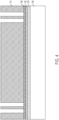
- FIG. 1 illustrates a release layer 104 coupled to a carrier substrate 106, and an insulating layer 102 coupled to the release layer 104.
- the carrier substrate 106 may include, for example, glass.
- the release layer 104 may include, for example, light-to-heat-conversion (LTHC) coating material.
- the insulating material 102 may include, for example, a polymer that can be patterned with light exposure and developed, such as polyimide, polybenzoxazole (PBO), or benzocyclobutene (BCB).
- a metal layer 108 is formed on the insulating layer 102.
- the metal layer 108 may be formed, for example, using physical vapor deposition (PVD) or sputtering.
- the metal layer 108 may include, for example, copper, or in some embodiments, the metal layer 108 may include two layers, such as a titanium layer coupled to the insulating layer 102 and a copper layer coupled to the titanium layer.
- a resist layer 110 is formed on the metal layer 108.
- the resist layer 110 may include photoresist.
- openings are formed in the resist layer 110.
- light exposure through a lithography mask followed by development may create openings in portions of the resist layer 110 that were exposed to light through the mask.
- metal pillars 112 are formed in the openings in the resist layer 110 using electroplating.
- the metal layer 108 may serve as a seed layer for the electroplating.
- the metal pillars 112 may include the same material as the metal layer 108, such as copper. It should be appreciated that while four metal pillars 112 are shown, there may be more metal pillars 112 (e.g., tens or hundreds) arranged two-dimensionally.
- the resist layer 110 is removed.
- a resist stripper may be used to remove the resist layer 110.
- Portions of the metal layer 108 that were previously under unexposed portions of the resist layer 110 are also removed.
- an anisotropic etch may be used to remove the metal layer 108, in which the metal layer 108 is etched faster than the metal pillars 112.
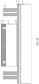
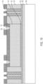
- FIG. 7 illustrates an ultrasound-on-a-chip 114 coupled to an insulating layer 116.
- openings are created in the insulating layer 116 (e.g., using photolithography).
- a resist layer 118 is formed on the insulating layer 116.
- openings are created in the resist layer 118 (e.g., using photolithography), where the openings created in the resist layer 118 extend into the openings created in the insulating layer 116.
- metal contacts 120 are formed within the openings in the resist layer 118 and the insulating layer 116.
- the metal contacts 120 may be formed by electroplating, and may include copper or a copper alloy.
- an under-bump metallurgy layer (not shown in FIG. 11 ) may be formed between the metal contacts 120 and the ultrasound-on-a-chip 114.
- the resist layer 118 is removed (e.g., using a resist stripper).
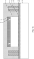
- a die-attach film (DAF) 122 is coupled to the insulating layer 102.
- the ultrasound-on-a-chip 114 is coupled to the die-attached film 122.
- encapsulation 124 is formed to encapsulate the ultrasound-on-a-chip 114, the insulating layer 116, the die-attach film 122, and the metal pillars 112.
- the encapsulation 124 may include a molding compound, a molding underfill, an epoxy, or a resin.
- the top surface of the encapsulation 124 extends above the top surfaces of the insulating layer 116 and the metal pillars 112.
- the top surfaces of the encapsulating 124 and the insulating layer 116 are planarized until the top surfaces of the top surfaces of the metal pillars 112 and the metal contacts 116 are exposed.
- CMP chemical mechanical planarization
- additional insulating material is added to the insulating layer 116, such that the insulating layer 116 covers the top surfaces of the metal contacts 120 and the metal pillars 112.
- openings are created in the insulating layer 116 above the metal contacts 120 and the metal pillars 112.
- photolithography may be used to create the openings.
- redistribution lines (RDL) 126 are formed in the openings in the insulating layer 116 and on the insulating layer 116. As shown, the RDL 126 may electrically connect certain of the metal contacts 120 to certain of the metal pillars 122.
- the RDL 126 may include metal traces and vias, may be formed using electroplating (including formation of a seed layer not shown), and may include metal such as aluminum, copper, tungsten, and/or alloys of these metals.
- the RDL 126 may include multiple layers of metal traces and vias.
- additional insulating material is added to the insulating layer 116 to cover the top surface of the RDL 126.
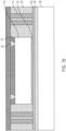
- the carrier substrate 106 and the release layer 104 are detached from the insulating layer 102.
- projecting light e.g., ultraviolet or laser
- the surface of the insulating layer 102 may also be cleaned to remove any residue.
- the structure of FIG. 21 is flipped over to arrive at the orientation of FIG. 22 .
- openings are created in the insulating layer 102.
- solder balls 128 are placed in the openings in the insulating layer 102.
- the solder balls 128 may be formed by electroplating.
- other forms of electrical connectors e.g., metal pillars
- an under-bump metallurgy layer (not shown in FIG. 24 ) may be formed between the solder balls 128 and the metal pillars 112.
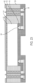
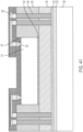
- FIG. 25 illustrates a release layer 134 coupled to a carrier substrate 136, an insulating layer 132 coupled to the release layer 134, and an interposer layer 130 coupled to the insulating layer 132.
- the interposer layer 130 may include, for example, aluminum nitride.
- openings are formed in the interposer layer 130.
- laser drilling may be used to form the openings.
- a metal layer 138 is formed on the interposer layer 130.
- the metal layer 138 may be formed, for example, using sputtering.
- the metal layer 138 may include, for example, copper, or in some embodiments, the metal layer 138 may include two layers, such as a titanium layer coupled to the interposer layer 130 and a copper layer coupled to the titanium layer.
- metal pillars 142 are formed in the openings in the resist layer 130 using electroplating.
- the metal layer 138 may serve as a seed layer for the electroplating.
- the metal pillars 142 may include the same material as the metal layer 138, such as copper. It should be appreciated that in addition to serving as electrical routing, the metal pillars 142 may also help to strengthen the interposer layer 130, which may be brittle.
- a resist layer 140 is formed on the metal layer 138 and the metal pillars 142.
- the resist layer 140 is patterned (e.g., using photolithography) to block the top surfaces of the metal pillars 142.
- non-blocked portions of the metal layer 108 are etched to electrically isolate the metal pillars 142.
- a timed etch or an anisotropic etch may be used instead of or in addition to using photolithography to block the metal pillars 142.
- the resist layer 140 is removed (e.g., using resist stripper).
- the carrier substrate 136 and the release layer 134 are detached from the insulating layer 132.
- openings are created in the insulating later 132.
- solder balls 144 are placed in the openings in the insulating layer 132.
- a thermal adhesive layer 150 is coupled to the interposer layer 142.
- the thermal adhesive layer 150 may include a silver-containing epoxy.
- the solder balls 144 are coupled to a printer circuit board (PCB) 148.
- PCB printer circuit board
- SMT surface-mount technology
- flip-chip soldering may be used to couple the solder balls 144 to the PCB 148.
- An underfill (e.g., epoxy) layer 146 is formed between the insulating layer 132 and the PCB 148.
- the solder balls 128 are coupled to the metal pillars 142.
- the metal pillars 112 are aligned with the metal pillars 142.
- surface-mount technology (SMT) or flip-chip soldering may be used to couple the solder balls 128 to the metal pillars 142.
- the interposer may provide electrical routing between the ultrasound-on-a-chip 114 and the PCB 148, as well as a heatsink for the ultrasound-on-a-chip 114.
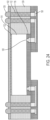
- FIGs. 38-42 illustrate cross-sections of various structures during packaging of an ultrasound-on-a-chip device using another process, in accordance with certain embodiments described herein.
- FIG. 38 illustrates the structure of FIG. 32 .
- the metal pillars 142 are extended upwards using electroplating. As can be seen, the metal pillars 142 extend beyond the top surface of the interposer layer 130.
- the ultrasound-on-a-chip 114 is coupled to the interposer layer 130 through the die-attach film 122.
- FIG. 41 further insulating material is added to the insulating layer 116.
- the encapsulation 124 is formed to encapsulate the ultrasound-on-a-chip 114, the insulating layer 116, the die-attach film 122, and the metal pillars 142, similar to in FIG. 16 .
- the RDL 126 is formed, similar to in FIGs. 18-21 .
- the carrier substrate 136 and the release layer 134 are detached from the insulating layer 132, the solder balls 144 are formed on the metal pillars 142, the solder balls 144 are coupled to the PCB 148, and an underfill layer 146 is formed between the insulating layer 132 and the PCB 148, similar to in FIGs. 33-36 .
- the process of FIGs. 38-42 may enable the ultrasound-on-a-chip 114 to be bound to the interposer layer 130 in a semiconductor foundry, where process control, quality, and yield may be high. Additionally, while the process of FIGs. 1-37 may require simultaneous bonding of the solder balls 128 to the metal pillars 142 and bonding of the insulating layer 102 to the thermal adhesive 150, the process of FIGs. 38-42 may eliminate the thermal adhesive layer 150.
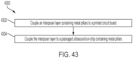
- FIG. 43 illustrates an example process 4300 for packaging an ultrasound-on-a-chip, in accordance with certain embodiments described herein.
- an interposer layer containing metal pillars is coupled to a printed circuit board.
- Act 4302 may correspond to the step illustrated in FIG. 36 .
- the interposer layer is coupled to a packaged ultrasound-on-a-chip containing metal pillars.
- Act 4304 may correspond to the step illustrated in FIG. 37 .
- the interposer layer may be coupled to the packaged ultrasound-on-a-chip through a thermal adhesive layer.
- FIG. 44 illustrates an example process 4400 for packaging an ultrasound-on-a-chip, in accordance with certain embodiments described herein.
- metal pillars are formed in an interposer layer.
- Act 4402 may correspond to the steps illustrated in FIGs. 38-39 .
- the interposer layer is coupled to an ultrasound-on-a-chip.
- Act 4404 may correspond to the step illustrated in FIG. 40 .
- a redistribution layer is formed on the packaged ultrasound-on-a-chip.
- Act 4406 may correspond to the step illustrated in FIG. 41 .
- a reference to "A and/or B", when used in conjunction with open-ended language such as “comprising” can refer, in one embodiment, to A only (optionally including elements other than B); in another embodiment, to B only (optionally including elements other than A); in yet another embodiment, to both A and B (optionally including other elements); etc.
- the phrase "at least one,” in reference to a list of one or more elements, should be understood to mean at least one element selected from any one or more of the elements in the list of elements, but not necessarily including at least one of each and every element specifically listed within the list of elements and not excluding any combinations of elements in the list of elements.
- This definition also allows that elements may optionally be present other than the elements specifically identified within the list of elements to which the phrase "at least one" refers, whether related or unrelated to those elements specifically identified.
- At least one of A and B can refer, in one embodiment, to at least one, optionally including more than one, A, with no B present (and optionally including elements other than B); in another embodiment, to at least one, optionally including more than one, B, with no A present (and optionally including elements other than A); in yet another embodiment, to at least one, optionally including more than one, A, and at least one, optionally including more than one, B (and optionally including other elements); etc.
- the terms “approximately” and “about” may be used to mean within ⁇ 20% of a target value in some embodiments, within ⁇ 10% of a target value in some embodiments, within ⁇ 5% of a target value in some embodiments, and yet within ⁇ 2% of a target value in some embodiments.
- the terms “approximately” and “about” may include the target value.
Landscapes
- Engineering & Computer Science (AREA)
- Health & Medical Sciences (AREA)
- Life Sciences & Earth Sciences (AREA)
- Mechanical Engineering (AREA)
- Physics & Mathematics (AREA)
- General Health & Medical Sciences (AREA)
- Pathology (AREA)
- Microelectronics & Electronic Packaging (AREA)
- Veterinary Medicine (AREA)
- Heart & Thoracic Surgery (AREA)
- Medical Informatics (AREA)
- Molecular Biology (AREA)
- Surgery (AREA)
- Animal Behavior & Ethology (AREA)
- Biomedical Technology (AREA)
- Public Health (AREA)
- Radiology & Medical Imaging (AREA)
- Nuclear Medicine, Radiotherapy & Molecular Imaging (AREA)
- Biophysics (AREA)
- General Physics & Mathematics (AREA)
- Biochemistry (AREA)
- Analytical Chemistry (AREA)
- Immunology (AREA)
- Chemical & Material Sciences (AREA)
- Computer Hardware Design (AREA)
- Transducers For Ultrasonic Waves (AREA)
- Ultra Sonic Daignosis Equipment (AREA)
- Investigating Or Analyzing Materials By The Use Of Ultrasonic Waves (AREA)
- Manufacturing & Machinery (AREA)
- Gynecology & Obstetrics (AREA)
- Computer Networks & Wireless Communication (AREA)
- Radar, Positioning & Navigation (AREA)
- Remote Sensing (AREA)
- Production Of Multi-Layered Print Wiring Board (AREA)
Applications Claiming Priority (2)
| Application Number | Priority Date | Filing Date | Title |
|---|---|---|---|
| US201862694810P | 2018-07-06 | 2018-07-06 | |
| PCT/US2019/040516 WO2020010207A1 (en) | 2018-07-06 | 2019-07-03 | Methods and apparatuses for packaging an ultrasound-on-a-chip |
Publications (4)
| Publication Number | Publication Date |
|---|---|
| EP3818372A1 EP3818372A1 (en) | 2021-05-12 |
| EP3818372A4 EP3818372A4 (en) | 2022-04-06 |
| EP3818372C0 EP3818372C0 (en) | 2024-10-30 |
| EP3818372B1 true EP3818372B1 (en) | 2024-10-30 |
Family
ID=69059840
Family Applications (1)
| Application Number | Title | Priority Date | Filing Date |
|---|---|---|---|
| EP19830619.3A Active EP3818372B1 (en) | 2018-07-06 | 2019-07-03 | Methods and apparatuses for packaging an ultrasound-on-a-chip |
Country Status (9)
| Country | Link |
|---|---|
| US (2) | US11018068B2 (https=) |
| EP (1) | EP3818372B1 (https=) |
| JP (1) | JP2021529459A (https=) |
| KR (1) | KR20210030951A (https=) |
| CN (1) | CN112368574B (https=) |
| AU (1) | AU2019297412A1 (https=) |
| CA (1) | CA3105492A1 (https=) |
| TW (1) | TW202011897A (https=) |
| WO (1) | WO2020010207A1 (https=) |
Families Citing this family (20)
| Publication number | Priority date | Publication date | Assignee | Title |
|---|---|---|---|---|
| EP3788798B1 (en) | 2018-05-03 | 2023-07-05 | BFLY Operations, Inc. | Ultrasonic transducers with pressure ports |
| JP2021529459A (ja) * | 2018-07-06 | 2021-10-28 | バタフライ ネットワーク,インコーポレイテッド | 超音波オンチップをパッケージングする方法及び装置 |
| WO2020069252A1 (en) | 2018-09-28 | 2020-04-02 | Butterfly Network, Inc. | Fabrication techniques and structures for gettering materials in ultrasonic transducer cavities |
| US11626343B2 (en) * | 2018-10-30 | 2023-04-11 | Taiwan Semiconductor Manufacturing Co., Ltd. | Semiconductor device with enhanced thermal dissipation and method for making the same |
| AU2019379545A1 (en) | 2018-11-13 | 2021-05-27 | Butterfly Network, Inc. | Getter technology for micromachined ultrasonic transducer cavities |
| US11571711B2 (en) | 2018-11-15 | 2023-02-07 | Bfly Operations, Inc. | Anti-stiction bottom cavity surface for micromachined ultrasonic transducer devices |
| AU2019392906A1 (en) | 2018-12-07 | 2021-07-22 | Octant, Inc. | Systems for protein-protein interaction screening |
| WO2020163595A1 (en) | 2019-02-07 | 2020-08-13 | Butterfly Network, Inc | Bi-layer metal electrode for micromachined ultrasonic transducer devices |
| WO2020176149A1 (en) | 2019-02-25 | 2020-09-03 | Butterfly Network, Inc. | Adaptive cavity thickness control for micromachined ultrasonic transducer devices |
| US12515240B2 (en) | 2019-04-12 | 2026-01-06 | Bfly Operations, Inc. | Segmented getter openings for micromachined ultrasound transducer devices |
| US11484911B2 (en) | 2019-04-12 | 2022-11-01 | Bfly Operations, Inc. | Bottom electrode via structures for micromachined ultrasonic transducer devices |
| US11501562B2 (en) | 2019-04-30 | 2022-11-15 | Bfly Operations, Inc. | Ultrasound face scanning and identification apparatuses and methods |
| US11684951B2 (en) | 2019-08-08 | 2023-06-27 | Bfly Operations, Inc. | Micromachined ultrasonic transducer devices having truncated circle shaped cavities |
| US11676922B2 (en) * | 2019-10-28 | 2023-06-13 | Qualcomm Incorporated | Integrated device comprising interconnect structures having an inner interconnect, a dielectric layer and a conductive layer |
| US11988640B2 (en) | 2020-03-11 | 2024-05-21 | Bfly Operations, Inc. | Bottom electrode material stack for micromachined ultrasonic transducer devices |
| US11776820B2 (en) * | 2020-09-30 | 2023-10-03 | Huawei Technologies Co., Ltd. | Vertical interconnection structure and manufacturing method thereof, packaged chip, and chip packaging method |
| TW202240165A (zh) | 2021-03-04 | 2022-10-16 | 美商蝴蝶營運公司 | 具有柱腳的微加工超音波換能器 |
| US12246348B2 (en) | 2021-03-04 | 2025-03-11 | BFLY Operations, Inc | Capacitive Micromachined ultrasonic transducers (CMUTs) having non-uniform pedestals |
| WO2022212671A1 (en) | 2021-04-01 | 2022-10-06 | Bfly Operations, Inc. | Apparatuses and methods for configuring ultrasound devices |
| KR20230084968A (ko) | 2021-12-06 | 2023-06-13 | 삼성전자주식회사 | 반도체 패키지 및 반도체 패키지의 제조 방법 |
Citations (2)
| Publication number | Priority date | Publication date | Assignee | Title |
|---|---|---|---|---|
| US20120146153A1 (en) * | 2010-12-08 | 2012-06-14 | Ying-Nan Wen | Chip package and method for forming the same |
| CN106449554A (zh) * | 2016-12-06 | 2017-02-22 | 苏州源戍微电子科技有限公司 | 带有封闭空腔的芯片嵌入式封装结构及其制作方法 |
Family Cites Families (31)
| Publication number | Priority date | Publication date | Assignee | Title |
|---|---|---|---|---|
| US7327554B2 (en) * | 2003-03-19 | 2008-02-05 | Ngk Spark Plug Co., Ltd. | Assembly of semiconductor device, interposer and substrate |
| US20060055024A1 (en) * | 2004-09-14 | 2006-03-16 | Staktek Group, L.P. | Adapted leaded integrated circuit module |
| US7741686B2 (en) | 2006-07-20 | 2010-06-22 | The Board Of Trustees Of The Leland Stanford Junior University | Trench isolated capacitive micromachined ultrasonic transducer arrays with a supporting frame |
| DE102007026445A1 (de) | 2007-06-06 | 2008-12-11 | Robert Bosch Gmbh | Mikromechanisches Bauelement und Verfahren zur Herstellung eines mikromechanischen Bauelements |
| US8193685B2 (en) | 2007-07-03 | 2012-06-05 | Koninklijke Philips Electronics N.V. | Thin film detector for presence detection |
| US7843022B2 (en) | 2007-10-18 | 2010-11-30 | The Board Of Trustees Of The Leland Stanford Junior University | High-temperature electrostatic transducers and fabrication method |
| US7781238B2 (en) | 2007-12-06 | 2010-08-24 | Robert Gideon Wodnicki | Methods of making and using integrated and testable sensor array |
| AU2009243918A1 (en) | 2008-05-07 | 2009-11-12 | Signostics Limited | Docking system for medical diagnostic scanning using a handheld device |
| US7838337B2 (en) * | 2008-12-01 | 2010-11-23 | Stats Chippac, Ltd. | Semiconductor device and method of forming an interposer package with through silicon vias |
| US7790492B1 (en) | 2009-06-13 | 2010-09-07 | Mwm Acoustics, Llc | Method for fabricating a transducer package with the transducer die unsupported by a substrate |
| US8207652B2 (en) | 2009-06-16 | 2012-06-26 | General Electric Company | Ultrasound transducer with improved acoustic performance |
| WO2011155638A1 (en) * | 2010-06-11 | 2011-12-15 | Nec Corporation | Method of redistributing functional element |
| SG190288A1 (en) | 2010-12-01 | 2013-06-28 | 1366 Tech Inc | Making semiconductor bodies from molten material using a free-standing interposer sheet |
| US9533873B2 (en) | 2013-02-05 | 2017-01-03 | Butterfly Network, Inc. | CMOS ultrasonic transducers and related apparatus and methods |
| WO2014123556A1 (en) * | 2013-02-05 | 2014-08-14 | Sound Technology Inc. | Ultrasound device |
| WO2014151525A2 (en) | 2013-03-15 | 2014-09-25 | Butterfly Network, Inc. | Complementary metal oxide semiconductor (cmos) ultrasonic transducers and methods for forming the same |
| US9633869B2 (en) * | 2013-08-16 | 2017-04-25 | Taiwan Semiconductor Manufacturing Company, Ltd. | Packages with interposers and methods for forming the same |
| CA2946133A1 (en) | 2014-04-18 | 2015-10-22 | Butterfly Network, Inc. | Ultrasonic transducers in complementary metal oxide semiconductor (cmos) wafers and related apparatus and methods |
| US9252127B1 (en) | 2014-07-10 | 2016-02-02 | Invensas Corporation | Microelectronic assemblies with integrated circuits and interposers with cavities, and methods of manufacture |
| US9067779B1 (en) | 2014-07-14 | 2015-06-30 | Butterfly Network, Inc. | Microfabricated ultrasonic transducers and related apparatus and methods |
| US20160009544A1 (en) * | 2015-03-02 | 2016-01-14 | Butterfly Network, Inc. | Microfabricated ultrasonic transducers and related apparatus and methods |
| US10276541B2 (en) * | 2015-06-30 | 2019-04-30 | Taiwan Semiconductor Manufacturing Company, Ltd. | 3D package structure and methods of forming same |
| CN113857023B (zh) * | 2016-06-20 | 2022-08-02 | 蝴蝶网络有限公司 | 用于微加工超声换能器的电接触布置 |
| US9922896B1 (en) | 2016-09-16 | 2018-03-20 | Taiwan Semiconductor Manufacturing Company, Ltd. | Info structure with copper pillar having reversed profile |
| US10196261B2 (en) | 2017-03-08 | 2019-02-05 | Butterfly Network, Inc. | Microfabricated ultrasonic transducers and related apparatus and methods |
| EP3642611B1 (en) | 2017-06-21 | 2024-02-14 | Butterfly Network, Inc. | Microfabricated ultrasonic transducer having individual cells with electrically isolated electrode sections |
| CN108155160A (zh) * | 2018-01-29 | 2018-06-12 | 中芯长电半导体(江阴)有限公司 | 指纹识别芯片的封装结构及封装方法 |
| EP3745961B1 (en) | 2018-01-30 | 2025-10-01 | BFLY Operations, Inc. | Methods and apparatuses for packaging an ultrasound-on-a-chip |
| US11590532B2 (en) | 2018-03-09 | 2023-02-28 | Bfly Operations, Inc. | Ultrasound transducer devices and methods for fabricating ultrasound transducer devices |
| TW201947717A (zh) | 2018-05-03 | 2019-12-16 | 美商蝴蝶網路公司 | 用於超音波晶片的垂直封裝及相關方法 |
| JP2021529459A (ja) * | 2018-07-06 | 2021-10-28 | バタフライ ネットワーク,インコーポレイテッド | 超音波オンチップをパッケージングする方法及び装置 |
-
2019
- 2019-07-03 JP JP2020571590A patent/JP2021529459A/ja active Pending
- 2019-07-03 CA CA3105492A patent/CA3105492A1/en active Pending
- 2019-07-03 EP EP19830619.3A patent/EP3818372B1/en active Active
- 2019-07-03 TW TW108123485A patent/TW202011897A/zh unknown
- 2019-07-03 US US16/502,553 patent/US11018068B2/en active Active
- 2019-07-03 WO PCT/US2019/040516 patent/WO2020010207A1/en not_active Ceased
- 2019-07-03 AU AU2019297412A patent/AU2019297412A1/en not_active Abandoned
- 2019-07-03 CN CN201980045060.6A patent/CN112368574B/zh active Active
- 2019-07-03 KR KR1020217003420A patent/KR20210030951A/ko not_active Ceased
-
2021
- 2021-03-04 US US17/191,829 patent/US11676874B2/en active Active
Patent Citations (2)
| Publication number | Priority date | Publication date | Assignee | Title |
|---|---|---|---|---|
| US20120146153A1 (en) * | 2010-12-08 | 2012-06-14 | Ying-Nan Wen | Chip package and method for forming the same |
| CN106449554A (zh) * | 2016-12-06 | 2017-02-22 | 苏州源戍微电子科技有限公司 | 带有封闭空腔的芯片嵌入式封装结构及其制作方法 |
Also Published As
| Publication number | Publication date |
|---|---|
| CN112368574A (zh) | 2021-02-12 |
| KR20210030951A (ko) | 2021-03-18 |
| AU2019297412A1 (en) | 2021-01-28 |
| US20200013691A1 (en) | 2020-01-09 |
| WO2020010207A1 (en) | 2020-01-09 |
| JP2021529459A (ja) | 2021-10-28 |
| CN112368574B (zh) | 2023-08-01 |
| EP3818372C0 (en) | 2024-10-30 |
| EP3818372A4 (en) | 2022-04-06 |
| US11676874B2 (en) | 2023-06-13 |
| EP3818372A1 (en) | 2021-05-12 |
| US20210296195A1 (en) | 2021-09-23 |
| US11018068B2 (en) | 2021-05-25 |
| CA3105492A1 (en) | 2020-01-09 |
| TW202011897A (zh) | 2020-04-01 |
Similar Documents
| Publication | Publication Date | Title |
|---|---|---|
| EP3818372B1 (en) | Methods and apparatuses for packaging an ultrasound-on-a-chip | |
| US20230106554A1 (en) | Microfeature workpieces and methods for forming interconnects in microfeature workpieces | |
| US11694943B2 (en) | Semiconductor device including heat dissipation structure and fabricating method of the same | |
| US7417311B2 (en) | Semiconductor device and method of fabricating the same | |
| TWI735702B (zh) | 積體扇出型封裝及其製造方法 | |
| US7948095B2 (en) | Semiconductor package and method of making the same | |
| US20210183832A1 (en) | Methods and apparatuses for packaging ultrasound-on-chip devices | |
| JP5608174B2 (ja) | 集積回路のための対面(f2f)ハイブリッド構造 | |
| US10290605B2 (en) | Fan-out package structure and method for forming the same | |
| US20070126030A1 (en) | Semiconductor device and method for manufacturing same, and semiconductor wafer | |
| TW202013650A (zh) | 晶片封裝結構的形成方法 | |
| TW202114121A (zh) | 半導體封裝及其製造方法 | |
| TW201919180A (zh) | 積體扇出型封裝及其形成方法 | |
| CN210489600U (zh) | 半导体封装 | |
| CN100514591C (zh) | 半导体封装的制造方法及所制成的封装 | |
| JP2008532307A5 (https=) | ||
| US11244894B2 (en) | Semiconductor packages | |
| US11158555B2 (en) | Package structure having sensor die with touch sensing electrode, and method of fabricating the same | |
| TWI920635B (zh) | 積體電路封裝體及其製造方法 | |
| US12183704B2 (en) | Semiconductor package and method for manufacturing the same | |
| TW202546999A (zh) | 積體電路封裝體及其製造方法 | |
| CN110931370A (zh) | 晶片封装结构的形成方法 | |
| JP2009049306A (ja) | 半導体装置 |
Legal Events
| Date | Code | Title | Description |
|---|---|---|---|
| STAA | Information on the status of an ep patent application or granted ep patent |
Free format text: STATUS: THE INTERNATIONAL PUBLICATION HAS BEEN MADE |
|
| PUAI | Public reference made under article 153(3) epc to a published international application that has entered the european phase |
Free format text: ORIGINAL CODE: 0009012 |
|
| STAA | Information on the status of an ep patent application or granted ep patent |
Free format text: STATUS: REQUEST FOR EXAMINATION WAS MADE |
|
| 17P | Request for examination filed |
Effective date: 20201221 |
|
| AK | Designated contracting states |
Kind code of ref document: A1 Designated state(s): AL AT BE BG CH CY CZ DE DK EE ES FI FR GB GR HR HU IE IS IT LI LT LU LV MC MK MT NL NO PL PT RO RS SE SI SK SM TR |
|
| DAV | Request for validation of the european patent (deleted) | ||
| DAX | Request for extension of the european patent (deleted) | ||
| A4 | Supplementary search report drawn up and despatched |
Effective date: 20220304 |
|
| RIC1 | Information provided on ipc code assigned before grant |
Ipc: G01N 29/24 20060101ALI20220228BHEP Ipc: B81B 7/00 20060101ALI20220228BHEP Ipc: A61B 8/00 20060101ALI20220228BHEP Ipc: G01N 29/22 20060101AFI20220228BHEP |
|
| RAP3 | Party data changed (applicant data changed or rights of an application transferred) |
Owner name: BFLY OPERATIONS, INC. |
|
| GRAP | Despatch of communication of intention to grant a patent |
Free format text: ORIGINAL CODE: EPIDOSNIGR1 |
|
| STAA | Information on the status of an ep patent application or granted ep patent |
Free format text: STATUS: GRANT OF PATENT IS INTENDED |
|
| INTG | Intention to grant announced |
Effective date: 20240528 |
|
| GRAS | Grant fee paid |
Free format text: ORIGINAL CODE: EPIDOSNIGR3 |
|
| GRAA | (expected) grant |
Free format text: ORIGINAL CODE: 0009210 |
|
| STAA | Information on the status of an ep patent application or granted ep patent |
Free format text: STATUS: THE PATENT HAS BEEN GRANTED |
|
| AK | Designated contracting states |
Kind code of ref document: B1 Designated state(s): AL AT BE BG CH CY CZ DE DK EE ES FI FR GB GR HR HU IE IS IT LI LT LU LV MC MK MT NL NO PL PT RO RS SE SI SK SM TR |
|
| REG | Reference to a national code |
Ref country code: GB Ref legal event code: FG4D |
|
| REG | Reference to a national code |
Ref country code: CH Ref legal event code: EP |
|
| REG | Reference to a national code |
Ref country code: DE Ref legal event code: R096 Ref document number: 602019061231 Country of ref document: DE |
|
| REG | Reference to a national code |
Ref country code: IE Ref legal event code: FG4D |
|
| U01 | Request for unitary effect filed |
Effective date: 20241108 |
|
| U07 | Unitary effect registered |
Designated state(s): AT BE BG DE DK EE FI FR IT LT LU LV MT NL PT RO SE SI Effective date: 20241118 |
|
| PG25 | Lapsed in a contracting state [announced via postgrant information from national office to epo] |
Ref country code: HR Free format text: LAPSE BECAUSE OF FAILURE TO SUBMIT A TRANSLATION OF THE DESCRIPTION OR TO PAY THE FEE WITHIN THE PRESCRIBED TIME-LIMIT Effective date: 20241030 Ref country code: IS Free format text: LAPSE BECAUSE OF FAILURE TO SUBMIT A TRANSLATION OF THE DESCRIPTION OR TO PAY THE FEE WITHIN THE PRESCRIBED TIME-LIMIT Effective date: 20250228 |
|
| PG25 | Lapsed in a contracting state [announced via postgrant information from national office to epo] |
Ref country code: ES Free format text: LAPSE BECAUSE OF FAILURE TO SUBMIT A TRANSLATION OF THE DESCRIPTION OR TO PAY THE FEE WITHIN THE PRESCRIBED TIME-LIMIT Effective date: 20241030 |
|
| PG25 | Lapsed in a contracting state [announced via postgrant information from national office to epo] |
Ref country code: NO Free format text: LAPSE BECAUSE OF FAILURE TO SUBMIT A TRANSLATION OF THE DESCRIPTION OR TO PAY THE FEE WITHIN THE PRESCRIBED TIME-LIMIT Effective date: 20250130 |
|
| PG25 | Lapsed in a contracting state [announced via postgrant information from national office to epo] |
Ref country code: GR Free format text: LAPSE BECAUSE OF FAILURE TO SUBMIT A TRANSLATION OF THE DESCRIPTION OR TO PAY THE FEE WITHIN THE PRESCRIBED TIME-LIMIT Effective date: 20250131 |
|
| PG25 | Lapsed in a contracting state [announced via postgrant information from national office to epo] |
Ref country code: PL Free format text: LAPSE BECAUSE OF FAILURE TO SUBMIT A TRANSLATION OF THE DESCRIPTION OR TO PAY THE FEE WITHIN THE PRESCRIBED TIME-LIMIT Effective date: 20241030 |
|
| PG25 | Lapsed in a contracting state [announced via postgrant information from national office to epo] |
Ref country code: RS Free format text: LAPSE BECAUSE OF FAILURE TO SUBMIT A TRANSLATION OF THE DESCRIPTION OR TO PAY THE FEE WITHIN THE PRESCRIBED TIME-LIMIT Effective date: 20250130 |
|
| PG25 | Lapsed in a contracting state [announced via postgrant information from national office to epo] |
Ref country code: SM Free format text: LAPSE BECAUSE OF FAILURE TO SUBMIT A TRANSLATION OF THE DESCRIPTION OR TO PAY THE FEE WITHIN THE PRESCRIBED TIME-LIMIT Effective date: 20241030 |
|
| PG25 | Lapsed in a contracting state [announced via postgrant information from national office to epo] |
Ref country code: SK Free format text: LAPSE BECAUSE OF FAILURE TO SUBMIT A TRANSLATION OF THE DESCRIPTION OR TO PAY THE FEE WITHIN THE PRESCRIBED TIME-LIMIT Effective date: 20241030 |
|
| PG25 | Lapsed in a contracting state [announced via postgrant information from national office to epo] |
Ref country code: CZ Free format text: LAPSE BECAUSE OF FAILURE TO SUBMIT A TRANSLATION OF THE DESCRIPTION OR TO PAY THE FEE WITHIN THE PRESCRIBED TIME-LIMIT Effective date: 20241030 |
|
| U20 | Renewal fee for the european patent with unitary effect paid |
Year of fee payment: 7 Effective date: 20250728 |
|
| PLBE | No opposition filed within time limit |
Free format text: ORIGINAL CODE: 0009261 |
|
| STAA | Information on the status of an ep patent application or granted ep patent |
Free format text: STATUS: NO OPPOSITION FILED WITHIN TIME LIMIT |
|
| 26N | No opposition filed |
Effective date: 20250731 |
|
| U1N | Appointed representative for the unitary patent procedure changed after the registration of the unitary effect |
Representative=s name: CARROLL, CHRISTOPHER P.; GB |
|
| REG | Reference to a national code |
Ref country code: CH Ref legal event code: H13 Free format text: ST27 STATUS EVENT CODE: U-0-0-H10-H13 (AS PROVIDED BY THE NATIONAL OFFICE) Effective date: 20260224 |
|
| GBPC | Gb: european patent ceased through non-payment of renewal fee |
Effective date: 20250703 |
|
| PG25 | Lapsed in a contracting state [announced via postgrant information from national office to epo] |
Ref country code: GB Free format text: LAPSE BECAUSE OF NON-PAYMENT OF DUE FEES Effective date: 20250703 |
|
| PG25 | Lapsed in a contracting state [announced via postgrant information from national office to epo] |
Ref country code: CH Free format text: LAPSE BECAUSE OF NON-PAYMENT OF DUE FEES Effective date: 20250731 |