EP3799542A1 - Procédé pour former un revêtement sur un dispositif électronique ou électrique - Google Patents
Procédé pour former un revêtement sur un dispositif électronique ou électrique Download PDFInfo
- Publication number
- EP3799542A1 EP3799542A1 EP20189052.2A EP20189052A EP3799542A1 EP 3799542 A1 EP3799542 A1 EP 3799542A1 EP 20189052 A EP20189052 A EP 20189052A EP 3799542 A1 EP3799542 A1 EP 3799542A1
- Authority
- EP
- European Patent Office
- Prior art keywords
- coating
- electronic
- electrical device
- component
- formula
- Prior art date
- Legal status (The legal status is an assumption and is not a legal conclusion. Google has not performed a legal analysis and makes no representation as to the accuracy of the status listed.)
- Withdrawn
Links
Images


Classifications
-
- H—ELECTRICITY
- H05—ELECTRIC TECHNIQUES NOT OTHERWISE PROVIDED FOR
- H05K—PRINTED CIRCUITS; CASINGS OR CONSTRUCTIONAL DETAILS OF ELECTRIC APPARATUS; MANUFACTURE OF ASSEMBLAGES OF ELECTRICAL COMPONENTS
- H05K3/00—Apparatus or processes for manufacturing printed circuits
- H05K3/22—Secondary treatment of printed circuits
- H05K3/28—Applying non-metallic protective coatings
- H05K3/285—Permanent coating compositions
-
- B—PERFORMING OPERATIONS; TRANSPORTING
- B05—SPRAYING OR ATOMISING IN GENERAL; APPLYING FLUENT MATERIALS TO SURFACES, IN GENERAL
- B05D—PROCESSES FOR APPLYING FLUENT MATERIALS TO SURFACES, IN GENERAL
- B05D1/00—Processes for applying liquids or other fluent materials
- B05D1/62—Plasma-deposition of organic layers
-
- B—PERFORMING OPERATIONS; TRANSPORTING
- B05—SPRAYING OR ATOMISING IN GENERAL; APPLYING FLUENT MATERIALS TO SURFACES, IN GENERAL
- B05D—PROCESSES FOR APPLYING FLUENT MATERIALS TO SURFACES, IN GENERAL
- B05D5/00—Processes for applying liquids or other fluent materials to surfaces to obtain special surface effects, finishes or structures
- B05D5/08—Processes for applying liquids or other fluent materials to surfaces to obtain special surface effects, finishes or structures to obtain an anti-friction or anti-adhesive surface
- B05D5/083—Processes for applying liquids or other fluent materials to surfaces to obtain special surface effects, finishes or structures to obtain an anti-friction or anti-adhesive surface involving the use of fluoropolymers
-
- C—CHEMISTRY; METALLURGY
- C23—COATING METALLIC MATERIAL; COATING MATERIAL WITH METALLIC MATERIAL; CHEMICAL SURFACE TREATMENT; DIFFUSION TREATMENT OF METALLIC MATERIAL; COATING BY VACUUM EVAPORATION, BY SPUTTERING, BY ION IMPLANTATION OR BY CHEMICAL VAPOUR DEPOSITION, IN GENERAL; INHIBITING CORROSION OF METALLIC MATERIAL OR INCRUSTATION IN GENERAL
- C23C—COATING METALLIC MATERIAL; COATING MATERIAL WITH METALLIC MATERIAL; SURFACE TREATMENT OF METALLIC MATERIAL BY DIFFUSION INTO THE SURFACE, BY CHEMICAL CONVERSION OR SUBSTITUTION; COATING BY VACUUM EVAPORATION, BY SPUTTERING, BY ION IMPLANTATION OR BY CHEMICAL VAPOUR DEPOSITION, IN GENERAL
- C23C16/00—Chemical coating by decomposition of gaseous compounds, without leaving reaction products of surface material in the coating, i.e. chemical vapour deposition [CVD] processes
- C23C16/44—Chemical coating by decomposition of gaseous compounds, without leaving reaction products of surface material in the coating, i.e. chemical vapour deposition [CVD] processes characterised by the method of coating
- C23C16/50—Chemical coating by decomposition of gaseous compounds, without leaving reaction products of surface material in the coating, i.e. chemical vapour deposition [CVD] processes characterised by the method of coating using electric discharges
- C23C16/513—Chemical coating by decomposition of gaseous compounds, without leaving reaction products of surface material in the coating, i.e. chemical vapour deposition [CVD] processes characterised by the method of coating using electric discharges using plasma jets
-
- H—ELECTRICITY
- H05—ELECTRIC TECHNIQUES NOT OTHERWISE PROVIDED FOR
- H05K—PRINTED CIRCUITS; CASINGS OR CONSTRUCTIONAL DETAILS OF ELECTRIC APPARATUS; MANUFACTURE OF ASSEMBLAGES OF ELECTRICAL COMPONENTS
- H05K5/00—Casings, cabinets or drawers for electric apparatus
- H05K5/06—Hermetically-sealed casings
- H05K5/065—Hermetically-sealed casings sealed by encapsulation, e.g. waterproof resin forming an integral casing, injection moulding
-
- H—ELECTRICITY
- H05—ELECTRIC TECHNIQUES NOT OTHERWISE PROVIDED FOR
- H05K—PRINTED CIRCUITS; CASINGS OR CONSTRUCTIONAL DETAILS OF ELECTRIC APPARATUS; MANUFACTURE OF ASSEMBLAGES OF ELECTRICAL COMPONENTS
- H05K2201/00—Indexing scheme relating to printed circuits covered by H05K1/00
- H05K2201/09—Shape and layout
- H05K2201/09818—Shape or layout details not covered by a single group of H05K2201/09009 - H05K2201/09809
- H05K2201/09872—Insulating conformal coating
-
- H—ELECTRICITY
- H05—ELECTRIC TECHNIQUES NOT OTHERWISE PROVIDED FOR
- H05K—PRINTED CIRCUITS; CASINGS OR CONSTRUCTIONAL DETAILS OF ELECTRIC APPARATUS; MANUFACTURE OF ASSEMBLAGES OF ELECTRICAL COMPONENTS
- H05K2203/00—Indexing scheme relating to apparatus or processes for manufacturing printed circuits covered by H05K3/00
- H05K2203/09—Treatments involving charged particles
- H05K2203/095—Plasma, e.g. for treating a substrate to improve adhesion with a conductor or for cleaning holes
Definitions
- This invention relates to protective coatings.
- the invention relates to substrates with protective coatings formed thereon, as well as methods of forming protective coatings on substrates.
- the problem is particularly acute in relation to small portable electronic equipment such as mobile phones, smartphones, pagers, radios, hearing aids, laptops, notebooks, tablet computers, phablets and personal digital assistants (PDAs), which can be exposed to significant liquid contamination when used outside or inside in close proximity to liquids.
- PDAs personal digital assistants
- Such devices are also prone to accidental exposure to liquids, for example if dropped in liquid or splashed.
- WO2007/083122 discloses electronic and electrical devices having a polymeric coating formed thereon by exposure to pulsed plasma comprising a particular monomer compound, for a sufficient period of time to allow a polymeric layer to form on the surface of the electrical or electronic devices.
- pulsed plasma comprising a particular monomer compound
- an item to be treated is placed within a plasma chamber together with material to be deposited in the gaseous state, a glow discharge is ignited within the chamber and a suitable voltage is applied, which may be pulsed.
- PCBs printed circuit boards
- An electronic substrate may, in principle, be any electronic or electrical device or component that comprises at least one exposed electrical or electronic contact point.
- Such substrates are particularly vulnerable, e.g. on account of electrochemical migration, and require highly effective barrier and repellent protection against liquids, frequently over complex surfaces, e.g. circuit board topographies.
- electrical or electronic contact points of such substrates may lose their functionality if coated with an overly thick protective layer, on account of increased electrical resistance.
- microphones or speakers on or in the vicinity of electronic substrates can become blocked or damaged if coated too thickly.
- Prior art coating technologies including sprays, dips, gas phase processing systems such as Parylene, and even plasma deposition, have thus far been unable to form, especially over complex surfaces, protective coatings that are of a sufficient thickness and resistance to provide a high degree of protection against liquids, without adversely affecting contact point functionality.
- P2i's Splash-proof technology where a thin repellent protective coating is applied to both the outside and the inside of an assembled electronic or electrical device. This restricts liquid ingress whilst additionally preventing any ingressed liquid spreading within the device. Thus, the vast majority of any liquid challenge is prevented from getting into the device in the first instance, whilst there is some additional protection within the device that does not interfere with the functionality of contact points.
- this technology generally only provides protection against splashing and not against immersion of the device into liquid.
- the inventors have now developed highly effective protective coatings, and methods for producing them, which may suitably be used with the aim of preventing the ingress of water into a treated electronic device or preventing and mitigating electrochemical migration on a surface comprising an electronic circuit, but which do not require masking during application.
- These coatings are based on plasma deposited monomer compounds.
- An aspect of the present invention provides an electronic or electrical device or component thereof having a coating formed thereon by exposing said electronic or electrical device or component thereof to a plasma comprising one or more monomer compounds for a sufficient period of time to allow a protective polymeric coating to form on a surface thereof; wherein the protective polymeric coating forms a physical barrier over a surface of the electronic or electrical device or component thereof;
- the coating protects the electronic or electrical device or component thereof by forming a physical barrier to mass and electron transport.
- the physical barrier restricts diffusion of water, O 2 or other ions with time/voltage.
- This physical barrier layer is distinct from the liquid repellent, typically water repellent, layer described in the prior art. It will be understood that the physical barrier layer of the present invention may be liquid repellent in addition to being a physical barrier, although the coating of the invention may be a physical barrier without being liquid repellent.
- the halogen may be chlorine or bromine, but fluorine is preferred for compliance with RoHS regulations (Restriction of Hazardous Substances).
- a is from 0 to 10, preferably from 0 to 6, optionally 2 to 4, most preferably 0 or 1.
- b is from 2 to 14, optionally from 2 to 10, preferably 3 to 7.
- Each of R 1 to R 9 is independently selected from hydrogen or halogen or an optionally substituted C 1 -C 6 branched or straight chain alkyl group.
- the alkyl group may be substituted or unsubstituted, saturated or unsaturated. When the alkyl group is substituted, the location or type of the substituent is not especially limited provided the resultant polymer provides an appropriate barrier layer. The skilled person would be aware of suitable substituents. If the alkyl group is substituted, a preferred substituent is halo, i.e. any of R 1 to R 9 may be haloalkyl, preferably fluoro alkyl. Any of the alkyl groups may also be substituted with one or more hydroxyl groups.
- alkyl group may comprise one or more alkene or alkyne groups.
- Each of R 1 to R 9 may be independently selected from hydrogen, methyl, ethyl, n-propyl, isopropyl, n-butyl, isobutyl, tert-butyl, sec-butyl, n-pentyl, neopentyl, n-hexyl, isohexyl, and 3-methylpentyl.
- each of R 1 to R 9 is independently selected from hydrogen or methyl.
- a and c are each independently 0 or 1; and b is from 3 to 7.
- each X is H. In an alternative preferred embodiment each X is F.
- R 1 and R 2 are both hydrogen.
- R 3 is hydrogen or methyl.
- R 1 and R 2 are both hydrogen and R 3 is hydrogen or methyl.
- R 8 is hydrogen and R 9 is C 1 -C 6 branched or straight chain alkyl group. In a particularly preferred embodiment, R 9 is methyl.
- each of R 4 to R 7 is hydrogen.
- the compound of formula I(a) has the following formula: where n is from 2 to 10.
- the compound of formula I(a) has the following formula: where n is from 2 to 10.
- the compound of formula I(a) may be selected from 1H,1H,2H,2H-perfluorohexyl acrylate (PFAC4), 1H,1H,2H,2H-perfluorooctyl acrylate (PFAC6), 1H,1H,2H,2H-perfluorodecyl acrylate (PFAC8) and 1H,1H,2H,2H-perfluorododecyl acrylate (PFAC10).
- PFAC4 1H,1H,2H,2H-perfluorohexyl acrylate
- PFAC6 1H,1H,2H,2H-perfluorooctyl acrylate
- PFAC8 1H,1H,2H,2H-perfluorodecyl acrylate
- PFAC10 1H,1H,2H,2H-perfluorododecyl acrylate
- the compound of formula I(a) may be selected from 1H,1H,2H,2H-pefluorohexyl methacrylate (PFMAC4), 1H,1H,2H,2H-perfluorooctyl methacrylate (PFMAC6) and 1H,1H,2H,2H-perfluorodecyl methacrylate (PFMAC8).
- PFMAC4 1H,1H,2H,2H-pefluorohexyl methacrylate
- PFMAC6 1H,1H,2H,2H-perfluorooctyl methacrylate
- PFMAC8 1H,1H,2H,2H-perfluorodecyl methacrylate
- the compound of formula I(a) has the following formula: where n is 2 to 12.
- the compound of formula I(a) may be selected from ethyl hexyl acrylate, hexyl acrylate, decyl acrylate, lauryl dodecyl acrylate and iso decyl acrylate.
- the compound of formula I(b) has the following formula: where n is from 3 to 13. Preferably n is 9.
- the compound of formula I(b) most preferably has the following formula: where n is from 3 to 13. n may be 6 to 10, preferably n is 9. ,i.e. vinyl decanoate.
- alkenyl alkyl alkanoates are contemplated as monomers for the present invention.
- Preferred monomers are vinyl alkyl alkanoates, such as vinyl hexanoate, vinyl heptanoate, vinyl octanoate, vinyl nonanoate, most preferably vinyl decanoate.
- the hydrogens may be substituted for another chemical group at one or more positions.
- the hydrogens may be substituted for halogen atoms, preferably fluoro.
- External surfaces may comprise the external surface of the electronic or electrical device or component thereof, for example the housing of a device, such as a smart phone, or external surfaces of individual components which will later be assembled into a device, such as PCBAs and microphones.
- internal surfaces may comprise, for example, the internal surface of a housing or the surface of the components housed within the housing.
- the electronic or electrical device or component thereof comprises a housing and wherein the coating forms a conformal physical barrier over an internal surface of the housing and/or surfaces of components within the housing.
- the coating forms a conformal physical barrier over an internal surface of the housing and/or surfaces of components within the housing.
- adequate protection is provided by the coating on the internal surfaces; the external surface of the housing may not be provided with a coating, which may be advantageous for cosmetic regions as well as reducing processing steps.
- CX 3 refers to the terminal groups in the side chain of the compounds of formulas I(a) and I(b).
- the coating formed by the present invention is more cross-linked than its conventionally polymerised counterpart, which explains its surprisingly good barrier performance.
- the polymer layer also provides repellence or resistance to liquid permeability.
- the coating may be electrically insulating.
- the combination of the barrier performance and optionally additionally the repellence of the coating of the present invention allows the coated electronic device or printed circuit board assembly (PCBA) to be submerged in water for at least 30 minutes without adverse effects.
- PCBA printed circuit board assembly
- the electronic or electrical device or component thereof can typically withstand immersion in up to 1m of water for over 30 minutes without failure or corrosion whilst power applied to the electronic or electrical device or component.
- the effectiveness of the coating can be determined by measuring its electrical resistance at a fixed voltage when submerged in water for a set time period; for example, when the protective polymeric coating is applied on a test printed circuit board (PCB). If it has a resistance of 8 MOhms or higher when submerged in water while a voltage of at least 16V/mm (for example 8V across a 0.5 mm gap between electrodes) is applied for a minimum of 13 minutes then it is an effective barrier coating and the coated electronic or electrical device or component thereof will pass successfully an IPX7 test.
- the IPX7 test is the Ingress Protection Marking which classifies and rates the degree of protection provided against water. In the IPX7 test for phones, the device is immersed in water under defined conditions of pressure and time (up to 1 m of submersion) for a duration of 30 minutes. The device has to be powered on during testing and functional after 24 hrs.
- barrier coatings of the present invention is believed to be caused by a mixture of cross linking and controlled fragmentation of the monomer during polymerisation.
- the ratio of these two functional groups is an indication that sufficient cross-linking and fragmentation has taken place and can be measured by the ratio of the intensities of the corresponding FTIR/ATR peaks.
- FIG 14 Possible mechanisms for cross linking of the monomer in the present invention are shown in Figure 14 which uses 1H, 1H, 2H, 2H-Perfluorodecyl acrylate (PFAC8) as an example.
- Cross linking between CF2 and CF3 is believed to be the most likely mechanism (i.e. scheme 3).
- the ratios of C O intensity/total intensity (area) of the ATR spectrum and CX 3 /total intensity both correlate to the coating's performance.
- the compound of formula I(a) comprises a compound of formula (II)
- the compound of formula (II) may be selected from 1H,1H,2H,2H-perfluorohexyl acrylate (PFAC4), 1H,1H,2H,2H-perfluorooctyl acrylate (PFAC6), 1H,1H,2H,2H-perfluorodecyl acrylate (PFAC8) and 1H,1H,2H,2H-perfluorododecyl acrylate (PFAC10).
- PFAC4 1H,1H,2H,2H-perfluorohexyl acrylate
- PFAC6 1H,1H,2H,2H-perfluorooctyl acrylate
- PFAC8 1H,1H,2H,2H-perfluorodecyl acrylate
- PFAC10 1H,1H,2H,2H-perfluorododecyl acrylate
- the compound of formula (III) may be selected from ethyl hexyl acrylate, hexyl acrylate, decyl acrylate, dodecyl (or lauryl)acrylate and iso decyl acrylate.
- the compound of formula I(a) comprises a compound of formula (IV)
- the compound of formula (IV) may be selected from 1H,1H,2H,2H-pefluorohexyl methacrylate (PFMAC4), 1H,1H,2H,2H-perfluorooctyl methacrylate (PFMAC6) and 1H,1H,2H,2H-perfluorodecyl methacrylate (PFMAC8).
- the compound of formula (I) comprises a compound of formula (V)
- the coating is preferably substantially pin-hole free to enable it to provide a physical barrier. Zooming into the coating, preferably ⁇ Z/d ⁇ 0.15, where ⁇ Z is the average height variation on an AFM line scan in nm (as shown in figure 2 ) and d is coating thickness in nm.
- a coating with a ⁇ Z/d ⁇ 0.15 is defined herein as being substantially pinhole free.
- the coating is preferably conformal, which means that it takes the 3D shape of the electronic or electrical device or component thereof and covers substantially an entire surface of the device. This has the advantage of ensuring that the coating has sufficient thickness to give optimal functionality over an entire surface of the device or component.
- the meaning of the term "covers substantially an entire surface” will depend to some extent on the type of surface to be covered. For example, for some components, it may be necessary for there to be complete coverage of the surface in order for the component to function after submersion in water. However, for other components or housings, small gaps in coverage may be tolerated.
- the coating may have a thickness of 50 to 10,000nm, optionally 50 to 8000nm, 100 to 5000nm, preferably 250nm - 5000nm, most preferably 250nm - 2000nm.
- the coating may be electrically insulating and be sufficiently compliant that electrical connectors can be joined to the electronic or electrical device or component thereof and an electrical connection made between the electrical connectors and electronic or electrical device or component thereof without the requirement to first remove the coating.
- the force exerted by the electrical connector on the coating is sufficient to alter the structure of or even break through the coating local to the electrical connector, allowing the electrical connection to be made.
- Electrical connectors can typically be joined to the electronic or electrical device or component in this way for coating thicknesses of under 5000nm, and for high performance coatings below 2000nm.
- the coating is electrically insulating and has a thickness of less than 1 micron and wherein a force of 5- 20g applied to the coating using a round probe with 1 mm diameter allows an electrical connection to be made with the electronic or electrical device or component thereof in the local area where the force has been applied.
- the coating is electrically insulating and has a thickness of 1-2.5 microns and wherein a force of 20-100g applied to the coating using a round probe with 1 mm diameter allows an electrical connection to be made in the local area of the coating where the force has been applied.
- the coating may have a higher density than that of the corresponding monomer from which it is formed.
- the increase in density may be at least 0.1 g/cm 3
- the increase in density is explained by the highly crosslinked coating.
- the high density of the coating improves the barrier properties of the coating.
- the coating may form a surface defined by a static water contact angle (WCA) of at least 70°. Coatings with a WCA of at least 90° may be described as liquid repellent (typically water repellent). In this case, the coating achieves liquid repellence in addition to providing a physical barrier.
- the coating may have a static water contact angle of at least 100°.
- the contact angle of a liquid on a solid substrate gives an indication of the surface energy which in turn illustrates the substrate's liquid repellence. Contact angles may be measured on a VCA Optima contact angle analyser, using 3 ⁇ l droplets of deionised water at room temperature.
- Another aspect of the invention provides a method for treating an electronic or electrical device or component as defined above, comprising:
- the process parameters may be altered, for example, power, flow rate of monomer and monomer flow/power ratio.
- the physical barrier is preferably a conformal physical barrier.
- the step of exposing said electronic or electrical device or component thereof to a plasma may comprise a two step process, in which the first and second steps comprise different plasma conditions.
- the step of exposing said electronic or electrical device or component thereto to a plasma may take place in a reaction chamber.
- the step of exposing said electronic or electrical device or component thereof to a plasma comprises a first continuous wave (CW) deposition step and second pulsed (PW) deposition step.
- CW continuous wave
- PW pulsed
- a first step may comprise optimising process parameters for surface preparation and cross-linking to occur and a second step may comprise adjusting the process parameters to allow for further cross linking and increased fragmentation to occur.
- optimal cross linking shown by lower CX 3 peak intensities in the FTIR/ATR spectra
- the step of exposing said electronic or electrical device or component thereof to a plasma may comprise a first continuous wave (CW) deposition step and second pulsed (PW) deposition step.
- CW continuous wave
- PW pulsed
- the continuous wave (CW) deposition step has been found to act as a substrate priming step which optimise the coating's performance.
- the applicants have discovered that inclusion of a CW step optimises the interface between the substrate surface and growing coating, both causing some etching of the substrate surface and growth of the polymer coating.
- Inclusion of the CW deposition step leads to homogenous growth of the coating and minimises the probability of the formation of defects in the coating.
- the pulsed (PW) deposition step has been found to be important in achieving good ingress of the coating into difficult to access areas.
- the applicants have surprisingly discovered that the quality and thickness of coating on internal surfaces can be optimised by adjusting the flow and power parameters. Increased power provided good quality coatings with the desired functionality on internal surfaces. Increased flow provided good quality coatings with the desired functionality on external surfaces.
- the ratio of power/flow (W/F) of the PW deposition step can be adjusted, depending on the desired properties of the coated substrate: increasing W/F causes an increase on the resistance and quality of the internal coating but a decrease in external resistance and quality.
- the flow rate of the monomer compound into the chamber may be much higher (on a per volume basis of the chamber) than that disclosed in the method of WO2007/083122 . It has been found that this high flow rate of the monomer compound surprisingly facilitates the formation of polymeric coatings having desirable liquid repellent and/or barrier properties even at thicknesses that offer a low electrical resistance.
- the exact flow rate of the monomer compound into the chamber may depend to some extent on the nature of the particular monomer compound being used, the nature of the substrate and the desired protective coating properties.
- the monomer compound is introduced into the chamber at a gas flow rate in the range of at least 1.5 sccm and preferably in the range of from 1.5 to 2500 sccm, optionally from 1.5 to 250 sccm, optionally from 1.5 to 200 sccm although this will depend on chamber volume.
- the gas flow rate may be in the range of 1.5 to 20 sccm.
- the monomer gas flow is calculated from the liquid monomer flow considering that the monomer in the chamber acts like an ideal gas.
- the invention resides in a method of forming a coating on an electronic or electrical device or component thereof, the method comprising: exposing said electronic or electrical device or component thereof in a chamber to a plasma comprising a monomer compound as defined above, preferably a pulsed plasma, for a sufficient period of time to allow a protective polymeric coating to form on the substrate, wherein during exposure of the substrate the monomer compound is introduced into the chamber at a rate in the range of from 100-10000 sccm/m 3 , more preferably in the range of 600-8000sccm/m 3 .
- the invention resides in a method of forming a coating on an electronic or electrical device or component thereof, the method comprising: exposing said substrate in a chamber to a plasma comprising a monomer as defined above, preferably a pulsed plasma, for a sufficient period of time to allow a protective polymeric coating to form on the substrate, wherein during exposure of the substrate the pulsed plasma has a peak power (e.g. on-phase) of at least 2W/litre.
- a plasma comprising a monomer as defined above, preferably a pulsed plasma
- this high average power density of the plasma surprisingly facilitates the formation of polymeric coatings having desirable liquid repellent and/or barrier properties even at thicknesses that offer a low electrical resistance. This is due to the increased cross linking and/or fragmentation that occurs at higher powers.
- the plasma may have an average power density in the range of from 0.001 to 20 W/litre.
- An average power density in the range of from 0.001-1 W/litre is particularly preferred for some type of compounds, for example compounds of formula II or formula III, n ⁇ 8.
- the plasma is a pulsed plasma in which pulses are applied in a sequence which yields a ratio of time on : time off in the range of from 0.001 to 1, optionally 0.002 to 0.5.
- time on may be 10-500 ⁇ s, preferably 35-45 ⁇ s, or 30-40 ⁇ s, such as about 36 ⁇ s and time off may be from 0.1 to 30 ms, preferably 0.1 to 15 ms, optionally from 5 to 15 ms, for example 6ms.
- Time on may be 35 ⁇ s, 40 ⁇ s, 45 ⁇ s.
- Time off may be 0.1, 1, 2, 3, 6, 8, 10, 15, 20, 25 or 30 ms.
- pulsed may mean that the plasma cycles between a state of no (or substantially no) plasma emission (off-state) and a state where a particular amount of plasma is emitted (on-state).
- pulsed may mean that there is continuous emission of plasma but that the amount of plasma cycles between an upper limit (on-state) and lower limit (off-state).
- the invention resides in a method of forming a coating on an electronic or electrical device or component thereof as defined above, the method comprising: exposing said substrate in a chamber to a plasma comprising a monomer compound, preferably a continuous plasma, for a sufficient period of time to allow a protective polymeric coating to form on the substrate, wherein during exposure of the substrate the continuous plasma has a power density of at least 2W/litre, preferably 20W/litre.
- the power to monomer flow ratio during the pulsed plasma may be between 2-60 W/sccm preferably 2-40 W/sccm, 2-25 W/sccm, 5-20 W/sccm,
- the invention resides in a method of forming a coating on an electronic or electrical device or component thereof as defined above, the method comprising: exposing said electronic or electrical device or component thereof in a chamber to a plasma comprising a monomer compound, preferably a pulsed plasma, for a sufficient period of time to allow a protective polymeric coating to form on the substrate, wherein during exposure of the substrate the pulsed plasma has a peak power to flow ratio of between 2 to 60 W/sccm, preferably 2 to 40 W/sccm, more preferably from 2-25 W/sccm, optionally 5-20 W/sccm.
- the invention resides in a method of forming a coating on an electronic or electrical device or component thereof, the method comprising: exposing said electronic or electrical device or component thereof in a chamber to a plasma comprising a monomer compound, preferably a continuous plasma, for a sufficient period of time to allow a protective polymeric coating to form on the substrate, wherein during exposure of the substrate the continuous plasma has a power to flow ratio of between 2 to 60 W/sccm, preferably 2 to 40 W/sccm, more preferably from 2-25 W/sccm, optionally 5-20 W/sccm.
- the step of exposing said electronic or electrical device or component thereof to a plasma may comprise a pulsed (PW) deposition step.
- the step of exposing said electronic or electrical device or component thereof to a plasma may comprise a continuous wave (CW) deposition step.
- the aspects of the invention each provide methods facilitating the formation of highly effective protective coatings that can be applied to electronic substrates without interfering adversely with contact points.
- An advantage is that the resultant coating is sufficiently compliant such that electrical connectors can be joined after coating the device during or after manufacture and assembly.
- the method includes the step of joining electrical connectors to the electronic or electrical device or component thereof after the coating has been applied. This has the advantage that electrical connectors can easily be joined to the electronic or electrical device or component thereof after coating the device or component during manufacture or assembly.
- a method of forming a coating on a substrate comprises: exposing said substrate in a chamber to a pulsed plasma for a sufficient period of time to allow a protective polymeric coating to form on the substrate, said plasma having a peak on-phase power of at least 2W/litre and comprising a hydrocarbon or fluorocarbon acrylate or methacrylate monomer compound, for example the compound of formula (la), introduced into the chamber during exposure of the substrate at a rate of at least 1.5 sccm or 2-100sccm or 2.5-20sccm.
- a method of forming a coating on a substrate comprises expositing said substrate in a chamber to a continuous plasma for a sufficient period of time to allow a protective polymeric coating to form on the substrate, said plasma having a peak power of at least 15W/I and comprising a hydrocarbon or fluorocarbon acrylate or methacrylate monomer compound, for example the compound of formula (la), introduced into the chamber during exposure of the substrate of at least 2.5sccm.
- the monomer may comprise a hydrocarbon or fluorocarbon acrylate or methacrylate.
- An embodiment of the invention provides a method for treating an electronic or electrical device or component, comprising:
- the compound may be selected from 1H,1H,2H,2H-pefluorohexyl acrylate (PFAC4), 1H,1H,2H,2H-perfluorooctyl acrylate (PFAC6), 1H,1H,2H,2H-perfluorodecyl acrylate (PFAC8) and 1H,1H,2H,2H-perfluorododecyl acrylate (PFAC10).
- PFAC4 1H,1H,2H,2H-pefluorohexyl acrylate
- PFAC6 1H,1H,2H,2H-perfluorooctyl acrylate
- PFAC8 1H,1H,2H,2H-perfluodecyl acrylate
- PFAC10 1H,1H,2H,2H-perfluorododecyl acrylate
- n 8
- X is F and R 3 is H, in which case the compound of formula I(a) is 1H,1H,2H,2H-heptadecafluorodecylacylate.
- the compound may be selected from 1H,1H,2H,2H-pefluorohexyl methacrylate (PFMAC4), 1H,1H,2H,2H-perfluorooctyl methacrylate (PFMAC6) and 1H,1H,2H,2H-perfluorodecyl methacrylate (PFMAC8).
- PFMAC4 1H,1H,2H,2H-pefluorohexyl methacrylate
- PFMAC6 1H,1H,2H,2H-perfluorooctyl methacrylate
- PFMAC8 1H,1H,2H,2H-perfluorodecyl methacrylate
- the compound of formula I(a) may be selected from ethyl hexyl acrylate, hexyl acrylate, decyl acrylate, lauryl dodecyl acrylate and iso decyl acrylate.
- the substrate may, in all aspects of the invention, advantageously be an electronic substrate.
- the electronic substrate may comprise an electronic or electrical device, i.e. any piece of electrical or electronic equipment.
- electrical and electronic devices include communications devices such as mobile phones, smartphones and pagers, radios, and sound and audio systems such as loudspeakers, microphones, ringers or buzzers, hearing aids, personal audio equipment such as personal CD, tape cassette or MP3 players, televisions, DVD players including portable DVD players, video recorders, digi and other set-top boxes such as Sky, computers and related components such as laptop, notebook, tablet, phablet or palmtop computers, personal digital assistants (PDAs), keyboards, or instrumentation, games consoles in particular hand-held playstations and the like, data storage devices, outdoor lighting systems or radio antenna and other forms of communication equipment.
- PDAs personal digital assistants
- the substrate may comprise or consist of an electronic component, e.g. a printed circuit board (PCB), a printed circuit board array (PCBA), a transistor, resistor, or semi-conductor chip.
- the electronic component may thus be an internal component of an electronic device, e.g. a mobile phone.
- the coatings of the invention are particularly valuable in preventing electrochemical migration in such components.
- the precise conditions under which the protective polymeric coating is formed in an effective manner will vary depending upon factors such as, without limitation, the nature of the monomer compound, the substrate, as well as the desired properties of the coating. These conditions can be determined using routine methods or, preferably, using the techniques and preferred features of the invention described herein, which work in particular synergy with the invention.
- Suitable plasmas for use in the methods of the invention include non-equilibrium plasmas such as those generated by radiofrequencies (Rf), microwaves or direct current (DC). They may operate at atmospheric or sub-atmospheric pressures as are known in the art. In particular however, they may be generated by radiofrequencies (Rf).
- Rf radiofrequencies
- DC direct current
- Various forms of equipment may be used to generate gaseous plasmas. Generally these comprise containers or plasma chambers in which plasmas may be generated. Particular examples of such equipment are described for instance in WO2005/089961 and WO02/28548 , the content of which is incorporated herein by reference, but many other conventional plasma generating apparatus are available.
- the substrate to be treated is placed within the plasma chamber together with the monomer compound, a glow discharge is ignited within the chamber, and a suitable voltage is applied.
- the voltage may be continuous wave or pulsed.
- Monomer may be introduced from the outset or following a period of preliminary continuous power plasma.
- the monomer compound will suitably be in a gaseous state in the plasma.
- the plasma may simply comprise a vapour of the monomer compound if present. Such a vapour may be formed in-situ, with the compounds being introduced into the chamber in liquid form.
- the monomer may also be combined with a carrier gas, in particular, an inert gas such as helium or argon.
- the monomer may be delivered into the chamber by way of an aerosol device such as a nebuliser or the like, as described for example in WO2003/097245 and WO03/101621 , the content of which is incorporated herein by reference.
- a carrier gas may not be required, which advantageously assists in achieving high flow rates.
- a preliminary continuous power plasma may be struck for example for from 10 seconds to 10 minutes for instance for about 20 to 60 seconds, within the chamber.
- This may act as a surface pre- treatment step, ensuring that the monomer compound attaches itself readily to the surface, so that as polymerisation occurs, the coating "grows" on the surface.
- the pre-treatment step may be conducted before monomer is introduced into the chamber, for example in the presence of inert gas, or simply in a residual atmosphere.
- Monomer may then be introduced into the chamber to allow polymerisation to proceed, either switching the plasma to a pulsed plasma, continuing with a continuous plasma or using a sequence of both continuous and pulsed plasma.
- a glow discharge is suitably ignited by applying a high frequency voltage, for example at 13.56MHz. This is suitably applied using electrodes, which may be internal or external to the chamber.
- Gases, vapours or aerosols may be drawn or pumped into the plasma chamber or region.
- gases or vapours may be drawn into the chamber as a result of a reduction in the pressure within the chamber, caused by use of an evacuating pump, or they may be pumped or injected into the chamber as is common in liquid handling.
- the gas, vapour or gas mixture may be supplied at a rate of at least 1.5 sccm and preferably in the range of from 1.5 to 100 sccm, more preferably 2.5 to 20 sccm, although this will depend on chamber volume. These amounts can be scaled up to larger systems on a chamber volume basis in accordance with the teaching herein.
- Polymerisation is suitably effected using vapours of the monomer compound, which are maintained at pressures of from 0.1 to 200 mtorr, suitably at about 15-150 mtorr.
- the applied fields may preferably provide a relatively high peak power density, e.g. as defined hereinabove in the method of the invention.
- the pulses may alternatively be applied in a sequence which yields a lower average power, for example in a sequence in which the ratio of the time on : time off is in the range of from 20:100 to 20 :20000 . Sequences with shorter time off periods may be preferred to maintain good power density.
- One example of a sequence is a sequence where power is on for 20 to 50 microseconds, for example 30 to 40 microseconds, such as about 36 microseconds, and off for from 5 to 30 milliseconds, for example 5 to 15 milliseconds, such as 6 milliseconds. This has been found to be of particular benefit when the monomer is a compound of formula (I).
- Preferred average powers obtained in this way in a 2.5 litre chamber were in the range of from 0.05 to 30W.
- relatively low average powers are preferred, e.g. in the range of from 0.1 to 5W, such as 0.15 to 0.5W in a 2.5 litre chamber.
- Higher average powers, for example over 10W have been found to have the advantage of aiding fragmentation of the monomer.
- the process temperatures may be ambient, or preferably slightly above ambient, such as in the range of from 30 to 60 °C, e.g. 35 to 55 °C. In some embodiments, the process temperature is kept below 40°C.
- a plasma chamber used may be of sufficient volume to accommodate multiple substrates, in particular when these are small in size, for example up to 20,000 PCBs can be processed at the same time with ease with the correct size equipment.
- a particularly suitable apparatus and method for producing coated substrates in accordance with the invention is described in WO2005/089961 , the content of which is hereby incorporated by reference.
- the dimensions of the chamber will be selected so as to accommodate the entirety of the particular substrate being treated.
- generally cuboid chambers may be suitable for a wide range of applications, but if necessary, elongate or rectangular chambers may be constructed or indeed cylindrical, or of any other suitable shape.
- the volume of the chamber may, for example be at least 1 litre, preferably at least 2 litres. In some applications, relatively small chambers with a volume of up to 13 litres or up to 10 litres are preferred. For large scale production, the volume of the chamber may suitably be up to 400 litres or higher.
- the chamber may be a sealable container, to allow for batch processes, or it may comprise inlets and outlets for substrates, to allow it to be utilised in a continuous process.
- the pressure conditions necessary for creating a plasma discharge within the chamber are maintained using high volume pumps, as is conventional for example in a device with a "whistling leak".
- high volume pumps as is conventional for example in a device with a "whistling leak”.
- electronic or electrical contact points of the substrate need not be masked during exposure, in particular for coating with a thickness below 5 ⁇ m, more preferably below 2 ⁇ m.
- such contacts and/or microphones/speakers are not masked during formation of the coating by any of the methods as described herein, leading to an advantageously simplified process.
- the invention has led to coatings that provide protective properties whilst maintaining contact point and microphone/speaker functionality.
- the invention resides in an electronic or electrical device or component thereof having a polymeric coating formed thereon by exposing said substrate to pulsed plasma comprising a monomer compound of formula (I) for a sufficient period of time to allow a protective polymeric coating to form on the substrate (for example according to any of the methods described herein), the coating having: a thickness of at least 50 nm and/or a surface defined by a static water contact angle (WCA) of at least 70°
- the invention resides in a substrate having a polymeric coating formed by any of the methods described herein.
- the invention also embraces coated substrates obtainable by any of the methods described herein.
- the invention resides in an electronic or electrical device, for example a mobile phone, comprising a housing and one or more internal electronic or electrical components with a coating formed thereon by any of the methods described herein.
- the housing need not comprise a coating.
- the device may advantageously pass standard IEC 60529 14.2.7 (IPX7).
- any of the coated electronic substrates described herein may preferably continue to function even after full immersion into water for at least 2 minutes, preferably at least 5 minutes.
- the electronic substrate will preferably continue to function for at least 30 minutes or more preferably at least two days.
- the expression "in a gaseous state” refers to gases or vapours, either alone or in mixture, as well as optionally aerosols.
- protecting polymeric coating refers to polymeric layers which provide some protection against liquid damage, for example by forming a barrier and optionally being liquid (such as oil- and/or water-) repellent.
- Sources of liquids from which the substrate is protected may include environmental liquids such as water, in particular rain, as well as liquids that may be accidentally spilled.
- the expression “during the exposure of the substrate” refers to a time period in which the substrate is within the chamber together with the plasma. In some embodiments of the invention, the expression may refer to the entire time period in which the substrate is within the chamber together with the plasma.
- FTIR/ATR refers to Fourier Transform Infra-Red Spectroscopy (FTIR) using an Attenuated Total Reflection (ATR) sampling technique. This is a well known technique which will be understood by a person skilled in the art. Typically the ATR sampling is performed using a diamond crystal.
- references to compound properties are - unless stated otherwise - to properties measured under ambient conditions, i.e. at atmospheric pressure and at a temperature of from 16 to 22 or 25 °C, or from 18 to 22 or 25 °C, for example about 20 °C or about 25 °C.
- Recited parameters e.g. in relation to thickness, hydrophobicity, density and roughness of the coating, may be measured by any of the techniques defined in the Examples, or using standard techniques in the art. Unless specified otherwise, all values recited herein may be measured or determined using standard techniques known to those skilled in the art.
- Plasma polymerization experiments were carried out in a cylindrical glass reactor vessel with a volume of 2.5 liters.
- the vessel was in two parts, coupled with a Viton O-ring to seal the two parts together under vacuum.
- One end of the reactor was connected to a liquid flow controller which was heated at 70°C and this was used for delivering monomer at a controlled flow rate.
- the other end of the reactor was connected to a metal pump line fitted with pressure gauges, pressure controlling valve, liquid nitrogen trap and a vacuum pump.
- a copper coil electrode was wrapped around the outside of the reactor (11 turns of 5 mm diameter piping) and this was connected to a RF power unit via an L-C matching network.
- the RF power unit was controlled by a pulse generator.
- the monomer used for this example was PFAC-8, i.e. 1H,1H,2H,2H-heptadecafluorodecylacrylate (CAS # 27905-45-9) of formula
- test PCBs and Si wafers were used.
- the Si wafers allow physical properties of the formed coating to be measured, for example AFM for surface morphology and XRR for coating density.
- the metal tracks of the test PCBs were gold coated copper.
- the Si wafers were placed on the top front side of the PCBs.
- Tables 1A-1D show the different process parameters for coatings formed in this example and the measured properties of these coatings.
- This test method has been devised to evaluate the ability of different coatings to provide an electrical barrier on printed circuit boards and predict the ability of a smart phone to pass the IEC 60529 14.2.7 (IPX7) test.
- the method is designed to be used with tap water.
- This test involves measuring the current voltage (IV) characteristics of a standardised printed circuit board (PCB) in water.
- PCB has been designed with spacing of 0.5 mm between electrodes to allow assessment of when electrochemical migration occurs across the tracks in water.
- the degree of electrochemical activity is quantified by measuring current flow; low current flow is indicative of a good quality coating.
- the method has proved to be extremely effective at discriminating between different coatings.
- the performance of the coatings can be quantified, e.g. as a resistance at 4 and 8V and 21 V.
- the measured resistance on the untreated test device is about 100 ohms when 16V/mm are applied.
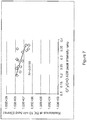
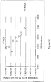
- the coated PCB 10 to be tested is placed into a beaker 12 of water 14 and connected to the electrical test apparatus via connections 16,18 as shown Figure 1 .
- the board is centred horizontally and vertically in the beaker to minimise effects of local ion concentration (vertical location of the board is very important; water level should be to the blue line).
- the power source is set to the desired voltage and the current is immediately monitored.
- the voltage applied is for example 8V and the PCB is held at the set voltage for 13 minutes, with the current being monitored continuously during this period.
- the coatings formed by the different process parameters are tested and the results are shown in Tables 1A-1D. It has been found that when coatings have resistance values higher that 8 MOhms, the coated device will pass successfully an IPX7 test. The nature of the device being coated (for example the type of smart phone) will influence the test, for example due to the variations in materials, ingress points, power consumption etc).
- the electrical conductivity of a coating can change significantly when a compressive stress is applied to the coating.
- the change in the electrical conductivity will depend on the amplitude of strain experienced by the coating, amount of defects and type of polymer matrix of the coating. This behaviour is explained on the basis of formation or destruction of a conductive network, which further depends on the viscosity (stiffness) of the polymer matrix.
- a contact force test is performed.
- the contact force test is an electrical test procedure which involves measuring the critical force (Fc) or pressure (Pc) that has to be applied to the insulating coating via a flat probe, for electrical break down through the coating to occur.
- the test can be used either on PCBs of smart phones or on strip boards (Test PCBs) which are placed as witness samples during processes.
- the test uses a flat probe e.g 1mm in diameter (or e.g a spherical probe of 2 mm diameter), contacting the planar film's surface.
- the probe is mounted on a support stand and the arrangement is such that variations in the force applied by the probe to the surface of the sample are immediately recorded by a weighing scale (or load cell) on which the sample is placed. With this arrangement the resolution in applied pressure is about 15 KPa (force 5g).
- the normal procedure is to manually ramp the force applied by the probe on the planar surface of the sample while observing the resistance between the probe and the conductive substrate.
- the force is manually or automatically increased up to the point (Fc) where current break down through the film occurs.
- This test allows the electrical insulation characteristics of the sample to be analyzed at a number of different points across the surface thus providing an idea of the uniformity of the surface layer.
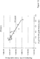
- Figure 19 is a graph of Fc against coating thickness for PFAC8 made according to Example 1. This shows that a force of 20-100g can be applied to the coating with a thickness of 1-2.5 microns to allow an electrical connection to be made.
- Typical Fc values for a coating with thickness of about 1000 nm is circa 35 g.
- the coating can achieve barrier functionality at relatively low (250-800nm) thickness, making it possible to achieve electrical contact after the application of relatively low ( ⁇ 15g) force. This is the advantage that coating of the present invention can provide when compared with other standard barrier coatings.
- the thickness of the coatings formed in Example 1 was measured using spectroscopic reflectometry apparatus (Filmetrics F20-UV) using optical constants verified by spectroscopic elipsometry.
- Spectroscopic ellipsometry is a technique for measuring the change in polarization between incident polarized light and the light after interaction with a sample (i.e. reflected, transmitted light etc).
- the change in polarization is quantified by the amplitude ratio ⁇ and phase difference ⁇ .
- a broad band light source is used to measure this variation over a range of wavelengths and the standard values of ⁇ and ⁇ are measured as a function of wavelength.
- the ITAC MNT Ellipsometer is an AutoSE from Horiba Yvon which has a wavelength range of 450 to 850nm. Many optical constants can be derived from the ⁇ and ⁇ values, such as film thickness and refractive index.
- Data collected from the sample measurements includes the intensities of the harmonics of the reflected or transmitted signal in the predefined spectral range. These are mathematically treated to extract intensity values called Is and Ic as f(I). Starting from Ic and Is the software calculates ⁇ and ⁇ . To extract parameters of interest, such as thickness or optical constants, a model has to be set up to allow theoretical calculation of ⁇ and ⁇ . The parameters of interest are determined by comparison of the theoretical and experimental data files to obtain the best fit (MSE or X 2 ). The best fit for a thin layer should give an X 2 ⁇ 3, for thicker coatings this value can be as large as 15.
- the model used is a three layer Laurentz model including PTFE on Si substrate finishing with a mixed layer (PTFE+voids) to account for surface roughness.
- Example 2 Examples of optical properties of coatings formed in Example 1 are given in table 2. This data relates to coatings 9 and 10 in Tables 1A-1D.
- Thickness of the coating is measured using a Filmetrics F20-UV spectroscopy reflectrometry apparatus.
- This instrument measures the coating's characteristics by reflecting light off the coating and analyzing the resulting reflectance spectrum over a range of wavelengths. Light reflected from different interfaces of the coating can be in- or out-of-phase so these reflections add or subtract, depending upon the wavelength of the incident light and the coating's thickness and index. The result is intensity oscillations in the reflectance spectrum that are characteristic of the coating.
- the Filmetrics software calculates a theoretical reflectance spectrum which matches as closely as possible to the measured spectrum. It begins with an initial guess for what the reflectance spectrum should look like, based on the nominal coating stack (layered structure). This includes information on the thickness (precision 0.2 nm) and the refractive index of the different layers and the substrate that make up the sample (refractive index values can be derived from spectroscopic ellipsometry). The theoretical reflectance spectrum is then adjusted by adjusting the coating's properties until a best fit to the measured spectrum is found. Measured coatings must be optically smooth and within the thickness range set by the system configuration requirements is shown in table 3.
- the thicknesses of the coatings produced in Example 1 are shown in Tables 1A-1D, which typical thickness being 750-3500nm.
- the surface morphology of the coatings is measured using atomic force microscopy (AFM).
- AFM atomic force microscopy
- Analyses are carried out with a Veeco Park Autoprobe AFM instrument, operated in the tapping imaging mode, using Ultrasharp NSC12, diving-board levers with spring constants in the range 4-14 N/m, and with resonant frequencies in the range 150-310 kHz.
- a high-aspect ratio probe, with a radius of curvature at the tip apex of ⁇ 10 nm and opening angle ⁇ 20° was used.
- Fields of view of 10x10, 5x5 and 1x1 ⁇ m 2 were imaged, with the larger field of view being the more informative.
- Surface roughness, RMS root mean square
- the ⁇ Z value indicated on the plot has been taken over an area of the graph that represents the majority of the coating. Peaks that lie above the ⁇ Z range indicate large particles and troughs that fall below the ⁇ Z range show voids or pinholes in the coating. The width of the peaks also gives an indication of the particle size.
- FTIR Fourier Transform Infra-Red Spectroscopy
- ATR Attenuated Total Reflection sampling technique
- the spectrometer used was an MIR Standard Perkin Elmer Frontier equipped with the Frontier UATR Diamond/ZnSe with 1 Reflection Top-Plate producing high quality spectra through the use of a pressure arm allowing good contact of the sample with the diamond crystal.
- Scan range of all measurements was 4,000-650cm -1 with 0.4cm -1 resolution and 10,000/1 pk-pk noise for a 5 second scan.
- the sample must be in direct contact with the ATR crystal.
- an infrared background is collected, in this case, from the clean ATR diamond crystal.
- the crystals are usually cleaned by using a solvent soaked piece of tissue. After the crystal area has been cleaned and the background collected, the solid sample is placed onto the small crystal area. The pressure arm should be positioned over the sample. Force is applied to the sample, pushing it onto the diamond surface. After the spectrum has been collected, the user must check that the crystal area is clean before placing the next sample on the crystal.
- a typical FTIR/ATR spectrum from a 1000 nm thick coating prepared as described in Example 1 is shown in Figure 3 . Assignments of the absorption peaks are also shown.
- the ratio between these two peak areas A (1335)/A(1737) is an important parameter characterising the chemistry and more specifically the degree of cross linking in the coating. It is found that coatings with thickness d>800 nm and A(1335)/A(1737 ⁇ 0.23 ⁇ 0.01 have undergone sufficient cross linking to have the desired functionality, providing they evenly cover the surface of the item under protection. It is established that plasma treatment would lead to the formation of a polymeric material that is far more cross-linked than its conventionally polymerised counterpart. Cross linking would affect the abundance of -CF3 functionalities in the coating.
- Coatings with thickness d ⁇ 800 nm require a correction to be applied to the measured ratio value A(1335)/A(1737) to account for the effect of the reduced thickness on the intensity of the selected FTIR/ATR peaks.
- Example 1 The physical density of the coatings prepared in Example 1 was estimated gravimetrically and also by XRR for more accuracy on very thin coatings.
- the polymer coating with the desired properties has been found to have a higher density than the corresponding monomer due to cross linking, which is in agreement with the FTIR/ATR findings.
- Table 5 shows the densities of three monomers and their resultant coatings, measured by X-ray Reflectometry (XRR).
- the coating formed from (I) is formed using the present method, whereas the coating formed from (II) is formed using a prior art method.
- the density values for Parylene C have been derived from literature [1].
- the coating (I) formed from PFAC8 according to the present invention is significantly denser than coating (III) formed from the same monomer using prior art methods. It is also significantly denser than Parylene C coating, a conventionally used barrier coating.
- the resistance value is resistance at 8V for 13 minutes in tap water and the FTIR/ATR ratio refers to A(1535)/A(1737).
- the monomers PFAC4 - PFAC10 all have formula (II) below, where n is 4 for PFAC4, 6 for PFAC6, 8 for PFAC8 and 10 for PFAC10.
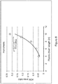
- Figure 8 is a graph of the FTIR/ATR critical ratio (i.e. below which the coating provides good barrier functionality) against n and shows that the selected ATR area ratio for each monomer increases exponentially with the length of the side chain. This is expected because during the ATR measurement the evanescent wave will interact with dipoles in the film in all orientations defining the C-F bonding envelope of each substance measured. As the length of the side chain increases the intensity of the peak representing the CF3 stretching will increase along with the signal of peaks representing CF2 and CF2-CF3 vibration modes.
- the ATR spectrum can be used. Table 7 shows the main features that differentiate the ATR spectra of the polymers.
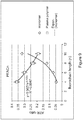
- Figure 13 shows the critical FTIR/ATR ratio values as a function of the side chain length for the initial perfluoro-acrylate (PFACn) or perfluoro methacrylate (PFMACn) monomer and the resulting plasma polymers.
- Parylene coatings with resistance values above 8MOhms can only be achieved with coatings thicker than 2500 nm. When reaching these high thicknesses the coating detrimentally affects the operation of the device, as shown by the high critical force of over >250g. With such a high thickness, the coating does not allow sufficient electrical contact to be made under typical contact forces, making masking of contacts a necessary operation before the coating application.
- This graph includes data from coatings formed from the following monomers: ethyl hexyl acrylate, hexyl acrylate, decyl acrylate, lauryl dodecyl acrylate and iso decyl acrylate. :
- the structures of decyl acrylate ( CAS no. 2156-96-9 ) and deodecyl(lauryl) acrylate ( CAS no. 2156-97-0 ) are given below:
- the applicants have been able to identify a general chemical structure for both fluorinated and non-fluorinated monomers which gives the desired performance.
- the monomer is a compound of formula I(a):
- All of the coatings in the examples have a coating thickness in the range of 250nm to 5000nm. On examination the coatings were found to be conformal and the fact that all of the coatings either exceed the IPX7 test or are close to it are indicative that they form physical barriers.
- the use of plasma polymerisation to deposit the coating has the advantage that the coating can be made sufficiently thick to provide a physical barrier whilst being significantly thinner than prior art conformal coatings. This thickness range has the advantage that it is sufficiently thick to form a physical barrier yet thin enough to allow electrical connections to be made without first removing it.
- plasma polymerisation also has the advantage that good ingress of the monomer during the plasma polymerisation technique ensures that the coating covers all of the desired areas, for example the entire external surface.
- the electronic or electrical device comprises a housing
- the entire internal surface of the housing can be coated (by exposing the open housing to the plasma) to protect the electronic components inside the housing once the device is assembled.
- Table 1A Process parameters and coating properties for coatings formed from PFAC8 Monomer: PFAC8 Parameter Units PW processes 1 2 3 4 5 6 7 CW time min 2 2 2 2 2 2 Ton ⁇ s 36 36 36 36 36 Toff ms 20 6 6 6 6 monomer pressure mtorr 30 30 30 30 30 PW power Watts 50 50 50 50 flow rate (STP) seem 2.2 2.20 2.2 2.63 2.63 Chamber T °C 45 45 45 45 45 45 PW time min 30 10 25 45 15 power/volume Watts/litre 20 20 20 20 20 20 20 power/flow Watts/(sccm) 23 23 23 19 19 monomer volume/min ml/min 0.028 0.028 0.028 0.034 0.034
- Table 1B Process parameters and coating properties for coatings formed from PFAC8 Monomer: PFAC8 Parameter Units PW processes 1 2 3 4 5 6 7 Thickness (d) Si nm 1000 1059 1185 1947 3770 934 1263 Thickness (d) SB nm
Landscapes
- Engineering & Computer Science (AREA)
- Physics & Mathematics (AREA)
- Plasma & Fusion (AREA)
- Chemical & Material Sciences (AREA)
- Microelectronics & Electronic Packaging (AREA)
- Manufacturing & Machinery (AREA)
- Metallurgy (AREA)
- Chemical Kinetics & Catalysis (AREA)
- Materials Engineering (AREA)
- Mechanical Engineering (AREA)
- General Chemical & Material Sciences (AREA)
- Organic Chemistry (AREA)
- Paints Or Removers (AREA)
- Application Of Or Painting With Fluid Materials (AREA)
- Addition Polymer Or Copolymer, Post-Treatments, Or Chemical Modifications (AREA)
- Non-Metallic Protective Coatings For Printed Circuits (AREA)
- Formation Of Insulating Films (AREA)
- Structures Or Materials For Encapsulating Or Coating Semiconductor Devices Or Solid State Devices (AREA)
- Polymerisation Methods In General (AREA)
- Organic Low-Molecular-Weight Compounds And Preparation Thereof (AREA)
Applications Claiming Priority (3)
| Application Number | Priority Date | Filing Date | Title |
|---|---|---|---|
| EP15386018 | 2015-06-09 | ||
| PCT/GB2016/051686 WO2016198855A1 (fr) | 2015-06-09 | 2016-06-08 | Procédé pour former un revêtement sur un dispositif électronique ou électrique |
| EP16739235.6A EP3308613B1 (fr) | 2015-06-09 | 2016-06-08 | Procédé pour former un revêtement sur un dispositif électronique ou électrique |
Related Parent Applications (1)
| Application Number | Title | Priority Date | Filing Date |
|---|---|---|---|
| EP16739235.6A Division EP3308613B1 (fr) | 2015-06-09 | 2016-06-08 | Procédé pour former un revêtement sur un dispositif électronique ou électrique |
Publications (1)
| Publication Number | Publication Date |
|---|---|
| EP3799542A1 true EP3799542A1 (fr) | 2021-03-31 |
Family
ID=53502598
Family Applications (2)
| Application Number | Title | Priority Date | Filing Date |
|---|---|---|---|
| EP20189052.2A Withdrawn EP3799542A1 (fr) | 2015-06-09 | 2016-06-08 | Procédé pour former un revêtement sur un dispositif électronique ou électrique |
| EP16739235.6A Not-in-force EP3308613B1 (fr) | 2015-06-09 | 2016-06-08 | Procédé pour former un revêtement sur un dispositif électronique ou électrique |
Family Applications After (1)
| Application Number | Title | Priority Date | Filing Date |
|---|---|---|---|
| EP16739235.6A Not-in-force EP3308613B1 (fr) | 2015-06-09 | 2016-06-08 | Procédé pour former un revêtement sur un dispositif électronique ou électrique |
Country Status (15)
| Country | Link |
|---|---|
| US (2) | US20190335592A1 (fr) |
| EP (2) | EP3799542A1 (fr) |
| JP (1) | JP2018522097A (fr) |
| KR (1) | KR20180016559A (fr) |
| CN (1) | CN108029198A (fr) |
| AU (1) | AU2016275276A1 (fr) |
| BE (1) | BE1023776B1 (fr) |
| BR (1) | BR112017026582A2 (fr) |
| ES (1) | ES2821323T3 (fr) |
| GB (1) | GB2556246B8 (fr) |
| IL (1) | IL256182A (fr) |
| MX (1) | MX2017015916A (fr) |
| PL (1) | PL3308613T3 (fr) |
| TW (1) | TW201706369A (fr) |
| WO (1) | WO2016198855A1 (fr) |
Families Citing this family (7)
| Publication number | Priority date | Publication date | Assignee | Title |
|---|---|---|---|---|
| GB201403558D0 (en) | 2014-02-28 | 2014-04-16 | P2I Ltd | Coating |
| CN109071966B (zh) | 2015-06-09 | 2022-07-22 | P2I有限公司 | 涂层 |
| CN211702520U (zh) * | 2019-01-11 | 2020-10-16 | 南京德朔实业有限公司 | 电动工具和电路板 |
| US20230227689A1 (en) * | 2020-05-18 | 2023-07-20 | Jiangsu Favored Nanotechnology Co., LTD | Water-resistant film layer and article thereof |
| WO2022008859A1 (fr) * | 2020-07-07 | 2022-01-13 | The Secretary Of State For Defence | Nouveaux substrats améliorés de spectroscopie raman |
| CN113025096A (zh) * | 2021-03-04 | 2021-06-25 | 江苏菲沃泰纳米科技股份有限公司 | 一种复合涂层、制备方法及器件 |
| CN118844121A (zh) | 2022-02-04 | 2024-10-25 | P2I有限公司 | 掩蔽方法和掩蔽产品 |
Citations (9)
| Publication number | Priority date | Publication date | Assignee | Title |
|---|---|---|---|---|
| WO2002028548A2 (fr) | 2000-10-04 | 2002-04-11 | Dow Corning Ireland Limited | Procede et appareil pour former un revetement |
| WO2003097245A2 (fr) | 2002-05-17 | 2003-11-27 | Surface Innovations Limited | Atomisation d'un precurseur dans un agent d'excitation pour revetir un substrat a distance |
| WO2003101621A2 (fr) | 2002-06-01 | 2003-12-11 | Surface Innovations Limited | Application d'un materiau de formation de revetement sur au moins un substrat |
| WO2005089961A1 (fr) | 2004-03-18 | 2005-09-29 | The Secretary Of State Of Defence | Revetement d'une couche polymere au moyen de plasma pulse a faible taux de poudre dans une chambre de depot en phase vapeur active par plasma a grand volume |
| WO2007083122A1 (fr) | 2006-01-20 | 2007-07-26 | P2I Ltd | Nouveaux produits |
| US20090267489A1 (en) * | 2004-12-20 | 2009-10-29 | Konica Minolta Holdings, Inc. | Gas barrier thin film laminate, gas barrier resin substrate and organic el device |
| US20120009231A1 (en) * | 2009-03-19 | 2012-01-12 | Anthony Herbert | Apparatus and method for deposition of functional coatings |
| WO2014026967A2 (fr) * | 2012-08-13 | 2014-02-20 | Europlasma Nv | Revêtements de surface |
| US20140322525A1 (en) * | 2011-09-07 | 2014-10-30 | Europlasma Nv | Surface polymer coatings |
Family Cites Families (2)
| Publication number | Priority date | Publication date | Assignee | Title |
|---|---|---|---|---|
| US5807612A (en) * | 1996-08-06 | 1998-09-15 | The University Of Connecticut | Method for coating metals by dip autopolymerization |
| WO2011068132A1 (fr) * | 2009-12-02 | 2011-06-09 | 東洋紡績株式会社 | Film de polyester à collage facile pour cellules solaires |
-
2016
- 2016-06-08 BE BE2016/5426A patent/BE1023776B1/nl not_active IP Right Cessation
- 2016-06-08 PL PL16739235T patent/PL3308613T3/pl unknown
- 2016-06-08 JP JP2017563970A patent/JP2018522097A/ja active Pending
- 2016-06-08 EP EP20189052.2A patent/EP3799542A1/fr not_active Withdrawn
- 2016-06-08 US US15/735,111 patent/US20190335592A1/en not_active Abandoned
- 2016-06-08 WO PCT/GB2016/051686 patent/WO2016198855A1/fr active Application Filing
- 2016-06-08 KR KR1020187000757A patent/KR20180016559A/ko unknown
- 2016-06-08 EP EP16739235.6A patent/EP3308613B1/fr not_active Not-in-force
- 2016-06-08 BR BR112017026582A patent/BR112017026582A2/pt not_active Application Discontinuation
- 2016-06-08 ES ES16739235T patent/ES2821323T3/es active Active
- 2016-06-08 MX MX2017015916A patent/MX2017015916A/es unknown
- 2016-06-08 CN CN201680046187.6A patent/CN108029198A/zh active Pending
- 2016-06-08 AU AU2016275276A patent/AU2016275276A1/en not_active Abandoned
- 2016-06-08 GB GB1800281.6A patent/GB2556246B8/en not_active Expired - Fee Related
- 2016-06-08 TW TW105118211A patent/TW201706369A/zh unknown
-
2017
- 2017-12-07 IL IL256182A patent/IL256182A/en unknown
-
2021
- 2021-08-03 US US17/392,931 patent/US20210368632A1/en not_active Abandoned
Patent Citations (10)
| Publication number | Priority date | Publication date | Assignee | Title |
|---|---|---|---|---|
| WO2002028548A2 (fr) | 2000-10-04 | 2002-04-11 | Dow Corning Ireland Limited | Procede et appareil pour former un revetement |
| WO2003097245A2 (fr) | 2002-05-17 | 2003-11-27 | Surface Innovations Limited | Atomisation d'un precurseur dans un agent d'excitation pour revetir un substrat a distance |
| WO2003101621A2 (fr) | 2002-06-01 | 2003-12-11 | Surface Innovations Limited | Application d'un materiau de formation de revetement sur au moins un substrat |
| WO2005089961A1 (fr) | 2004-03-18 | 2005-09-29 | The Secretary Of State Of Defence | Revetement d'une couche polymere au moyen de plasma pulse a faible taux de poudre dans une chambre de depot en phase vapeur active par plasma a grand volume |
| US20090267489A1 (en) * | 2004-12-20 | 2009-10-29 | Konica Minolta Holdings, Inc. | Gas barrier thin film laminate, gas barrier resin substrate and organic el device |
| WO2007083122A1 (fr) | 2006-01-20 | 2007-07-26 | P2I Ltd | Nouveaux produits |
| US20100189914A1 (en) * | 2006-01-20 | 2010-07-29 | P2I Ltd. | Novel products |
| US20120009231A1 (en) * | 2009-03-19 | 2012-01-12 | Anthony Herbert | Apparatus and method for deposition of functional coatings |
| US20140322525A1 (en) * | 2011-09-07 | 2014-10-30 | Europlasma Nv | Surface polymer coatings |
| WO2014026967A2 (fr) * | 2012-08-13 | 2014-02-20 | Europlasma Nv | Revêtements de surface |
Non-Patent Citations (1)
| Title |
|---|
| CHEMICAL ABSTRACTS, Columbus, Ohio, US; abstract no. 52591-27-2 |
Also Published As
| Publication number | Publication date |
|---|---|
| AU2016275276A1 (en) | 2018-02-01 |
| BR112017026582A2 (pt) | 2018-08-14 |
| MX2017015916A (es) | 2018-08-21 |
| EP3308613A1 (fr) | 2018-04-18 |
| GB201800281D0 (en) | 2018-02-21 |
| PL3308613T3 (pl) | 2020-11-16 |
| BE1023776B1 (nl) | 2017-07-20 |
| US20210368632A1 (en) | 2021-11-25 |
| WO2016198855A1 (fr) | 2016-12-15 |
| TW201706369A (zh) | 2017-02-16 |
| BE1023776A1 (nl) | 2017-07-18 |
| US20190335592A1 (en) | 2019-10-31 |
| GB2556246B (en) | 2019-06-12 |
| ES2821323T3 (es) | 2021-04-26 |
| GB2556246A (en) | 2018-05-23 |
| CN108029198A (zh) | 2018-05-11 |
| GB2556246C (en) | 2019-06-26 |
| IL256182A (en) | 2018-02-28 |
| GB2556246A8 (en) | 2020-08-19 |
| KR20180016559A (ko) | 2018-02-14 |
| GB2556246B8 (en) | 2020-08-19 |
| JP2018522097A (ja) | 2018-08-09 |
| EP3308613B1 (fr) | 2020-08-05 |
Similar Documents
| Publication | Publication Date | Title |
|---|---|---|
| US20210368632A1 (en) | Method for forming a coating on an electronic or electrical device | |
| US20210355341A1 (en) | Coatings | |
| US20140141674A1 (en) | Apparatus and methods for plasma enhanced chemical vapor deposition of dielectric/polymer coatings | |
| US20200032072A1 (en) | Coating | |
| CN111607262B (zh) | 带有聚合物纳米涂层的基材及形成聚合物纳米涂层的方法 | |
| US20210013646A1 (en) | Method of forming a protected connection and connector comprising said connection | |
| WO2014078497A1 (fr) | Appareil et procédés pour dépôt chimique en phase vapeur activé par plasma de revêtements diélectriques/polymères | |
| JP2017509476A (ja) | コーティング | |
| BE1025386B1 (nl) | Coating |
Legal Events
| Date | Code | Title | Description |
|---|---|---|---|
| PUAI | Public reference made under article 153(3) epc to a published international application that has entered the european phase |
Free format text: ORIGINAL CODE: 0009012 |
|
| STAA | Information on the status of an ep patent application or granted ep patent |
Free format text: STATUS: THE APPLICATION HAS BEEN PUBLISHED |
|
| AC | Divisional application: reference to earlier application |
Ref document number: 3308613 Country of ref document: EP Kind code of ref document: P |
|
| AK | Designated contracting states |
Kind code of ref document: A1 Designated state(s): AL AT BE BG CH CY CZ DE DK EE ES FI FR GB GR HR HU IE IS IT LI LT LU LV MC MK MT NL NO PL PT RO RS SE SI SK SM TR |
|
| STAA | Information on the status of an ep patent application or granted ep patent |
Free format text: STATUS: THE APPLICATION IS DEEMED TO BE WITHDRAWN |
|
| 18D | Application deemed to be withdrawn |
Effective date: 20211001 |