EP3786697B1 - Optische vorrichtung und verwendung davon - Google Patents
Optische vorrichtung und verwendung davon Download PDFInfo
- Publication number
- EP3786697B1 EP3786697B1 EP19792177.8A EP19792177A EP3786697B1 EP 3786697 B1 EP3786697 B1 EP 3786697B1 EP 19792177 A EP19792177 A EP 19792177A EP 3786697 B1 EP3786697 B1 EP 3786697B1
- Authority
- EP
- European Patent Office
- Prior art keywords
- base layer
- optical device
- liquid crystal
- layer
- heat shrinkable
- Prior art date
- Legal status (The legal status is an assumption and is not a legal conclusion. Google has not performed a legal analysis and makes no representation as to the accuracy of the status listed.)
- Active
Links
Images

Classifications
-
- G—PHYSICS
- G02—OPTICS
- G02F—OPTICAL DEVICES OR ARRANGEMENTS FOR THE CONTROL OF LIGHT BY MODIFICATION OF THE OPTICAL PROPERTIES OF THE MEDIA OF THE ELEMENTS INVOLVED THEREIN; NON-LINEAR OPTICS; FREQUENCY-CHANGING OF LIGHT; OPTICAL LOGIC ELEMENTS; OPTICAL ANALOGUE/DIGITAL CONVERTERS
- G02F1/00—Devices or arrangements for the control of the intensity, colour, phase, polarisation or direction of light arriving from an independent light source, e.g. switching, gating or modulating; Non-linear optics
- G02F1/01—Devices or arrangements for the control of the intensity, colour, phase, polarisation or direction of light arriving from an independent light source, e.g. switching, gating or modulating; Non-linear optics for the control of the intensity, phase, polarisation or colour
- G02F1/13—Devices or arrangements for the control of the intensity, colour, phase, polarisation or direction of light arriving from an independent light source, e.g. switching, gating or modulating; Non-linear optics for the control of the intensity, phase, polarisation or colour based on liquid crystals, e.g. single liquid crystal display cells
- G02F1/133—Constructional arrangements; Operation of liquid crystal cells; Circuit arrangements
- G02F1/1333—Constructional arrangements; Manufacturing methods
- G02F1/133305—Flexible substrates, e.g. plastics, organic film
-
- C—CHEMISTRY; METALLURGY
- C08—ORGANIC MACROMOLECULAR COMPOUNDS; THEIR PREPARATION OR CHEMICAL WORKING-UP; COMPOSITIONS BASED THEREON
- C08J—WORKING-UP; GENERAL PROCESSES OF COMPOUNDING; AFTER-TREATMENT NOT COVERED BY SUBCLASSES C08B, C08C, C08F, C08G or C08H
- C08J5/00—Manufacture of articles or shaped materials containing macromolecular substances
- C08J5/18—Manufacture of films or sheets
-
- C—CHEMISTRY; METALLURGY
- C08—ORGANIC MACROMOLECULAR COMPOUNDS; THEIR PREPARATION OR CHEMICAL WORKING-UP; COMPOSITIONS BASED THEREON
- C08L—COMPOSITIONS OF MACROMOLECULAR COMPOUNDS
- C08L1/00—Compositions of cellulose, modified cellulose or cellulose derivatives
- C08L1/08—Cellulose derivatives
- C08L1/10—Esters of organic acids, i.e. acylates
- C08L1/12—Cellulose acetate
-
- C—CHEMISTRY; METALLURGY
- C08—ORGANIC MACROMOLECULAR COMPOUNDS; THEIR PREPARATION OR CHEMICAL WORKING-UP; COMPOSITIONS BASED THEREON
- C08L—COMPOSITIONS OF MACROMOLECULAR COMPOUNDS
- C08L67/00—Compositions of polyesters obtained by reactions forming a carboxylic ester link in the main chain; Compositions of derivatives of such polymers
- C08L67/02—Polyesters derived from dicarboxylic acids and dihydroxy compounds
-
- G—PHYSICS
- G02—OPTICS
- G02F—OPTICAL DEVICES OR ARRANGEMENTS FOR THE CONTROL OF LIGHT BY MODIFICATION OF THE OPTICAL PROPERTIES OF THE MEDIA OF THE ELEMENTS INVOLVED THEREIN; NON-LINEAR OPTICS; FREQUENCY-CHANGING OF LIGHT; OPTICAL LOGIC ELEMENTS; OPTICAL ANALOGUE/DIGITAL CONVERTERS
- G02F1/00—Devices or arrangements for the control of the intensity, colour, phase, polarisation or direction of light arriving from an independent light source, e.g. switching, gating or modulating; Non-linear optics
- G02F1/01—Devices or arrangements for the control of the intensity, colour, phase, polarisation or direction of light arriving from an independent light source, e.g. switching, gating or modulating; Non-linear optics for the control of the intensity, phase, polarisation or colour
- G02F1/13—Devices or arrangements for the control of the intensity, colour, phase, polarisation or direction of light arriving from an independent light source, e.g. switching, gating or modulating; Non-linear optics for the control of the intensity, phase, polarisation or colour based on liquid crystals, e.g. single liquid crystal display cells
- G02F1/133—Constructional arrangements; Operation of liquid crystal cells; Circuit arrangements
- G02F1/1333—Constructional arrangements; Manufacturing methods
- G02F1/1337—Surface-induced orientation of the liquid crystal molecules, e.g. by alignment layers
-
- G—PHYSICS
- G02—OPTICS
- G02F—OPTICAL DEVICES OR ARRANGEMENTS FOR THE CONTROL OF LIGHT BY MODIFICATION OF THE OPTICAL PROPERTIES OF THE MEDIA OF THE ELEMENTS INVOLVED THEREIN; NON-LINEAR OPTICS; FREQUENCY-CHANGING OF LIGHT; OPTICAL LOGIC ELEMENTS; OPTICAL ANALOGUE/DIGITAL CONVERTERS
- G02F1/00—Devices or arrangements for the control of the intensity, colour, phase, polarisation or direction of light arriving from an independent light source, e.g. switching, gating or modulating; Non-linear optics
- G02F1/01—Devices or arrangements for the control of the intensity, colour, phase, polarisation or direction of light arriving from an independent light source, e.g. switching, gating or modulating; Non-linear optics for the control of the intensity, phase, polarisation or colour
- G02F1/13—Devices or arrangements for the control of the intensity, colour, phase, polarisation or direction of light arriving from an independent light source, e.g. switching, gating or modulating; Non-linear optics for the control of the intensity, phase, polarisation or colour based on liquid crystals, e.g. single liquid crystal display cells
- G02F1/133—Constructional arrangements; Operation of liquid crystal cells; Circuit arrangements
- G02F1/1333—Constructional arrangements; Manufacturing methods
- G02F1/1339—Gaskets; Spacers; Sealing of cells
-
- G—PHYSICS
- G02—OPTICS
- G02F—OPTICAL DEVICES OR ARRANGEMENTS FOR THE CONTROL OF LIGHT BY MODIFICATION OF THE OPTICAL PROPERTIES OF THE MEDIA OF THE ELEMENTS INVOLVED THEREIN; NON-LINEAR OPTICS; FREQUENCY-CHANGING OF LIGHT; OPTICAL LOGIC ELEMENTS; OPTICAL ANALOGUE/DIGITAL CONVERTERS
- G02F1/00—Devices or arrangements for the control of the intensity, colour, phase, polarisation or direction of light arriving from an independent light source, e.g. switching, gating or modulating; Non-linear optics
- G02F1/01—Devices or arrangements for the control of the intensity, colour, phase, polarisation or direction of light arriving from an independent light source, e.g. switching, gating or modulating; Non-linear optics for the control of the intensity, phase, polarisation or colour
- G02F1/13—Devices or arrangements for the control of the intensity, colour, phase, polarisation or direction of light arriving from an independent light source, e.g. switching, gating or modulating; Non-linear optics for the control of the intensity, phase, polarisation or colour based on liquid crystals, e.g. single liquid crystal display cells
- G02F1/133—Constructional arrangements; Operation of liquid crystal cells; Circuit arrangements
- G02F1/1333—Constructional arrangements; Manufacturing methods
- G02F1/1343—Electrodes
- G02F1/134309—Electrodes characterised by their geometrical arrangement
-
- G—PHYSICS
- G02—OPTICS
- G02F—OPTICAL DEVICES OR ARRANGEMENTS FOR THE CONTROL OF LIGHT BY MODIFICATION OF THE OPTICAL PROPERTIES OF THE MEDIA OF THE ELEMENTS INVOLVED THEREIN; NON-LINEAR OPTICS; FREQUENCY-CHANGING OF LIGHT; OPTICAL LOGIC ELEMENTS; OPTICAL ANALOGUE/DIGITAL CONVERTERS
- G02F1/00—Devices or arrangements for the control of the intensity, colour, phase, polarisation or direction of light arriving from an independent light source, e.g. switching, gating or modulating; Non-linear optics
- G02F1/01—Devices or arrangements for the control of the intensity, colour, phase, polarisation or direction of light arriving from an independent light source, e.g. switching, gating or modulating; Non-linear optics for the control of the intensity, phase, polarisation or colour
- G02F1/13—Devices or arrangements for the control of the intensity, colour, phase, polarisation or direction of light arriving from an independent light source, e.g. switching, gating or modulating; Non-linear optics for the control of the intensity, phase, polarisation or colour based on liquid crystals, e.g. single liquid crystal display cells
- G02F1/137—Devices or arrangements for the control of the intensity, colour, phase, polarisation or direction of light arriving from an independent light source, e.g. switching, gating or modulating; Non-linear optics for the control of the intensity, phase, polarisation or colour based on liquid crystals, e.g. single liquid crystal display cells characterised by the electro-optical or magneto-optical effect, e.g. field-induced phase transition, orientation effect, guest-host interaction or dynamic scattering
-
- G—PHYSICS
- G02—OPTICS
- G02F—OPTICAL DEVICES OR ARRANGEMENTS FOR THE CONTROL OF LIGHT BY MODIFICATION OF THE OPTICAL PROPERTIES OF THE MEDIA OF THE ELEMENTS INVOLVED THEREIN; NON-LINEAR OPTICS; FREQUENCY-CHANGING OF LIGHT; OPTICAL LOGIC ELEMENTS; OPTICAL ANALOGUE/DIGITAL CONVERTERS
- G02F1/00—Devices or arrangements for the control of the intensity, colour, phase, polarisation or direction of light arriving from an independent light source, e.g. switching, gating or modulating; Non-linear optics
- G02F1/01—Devices or arrangements for the control of the intensity, colour, phase, polarisation or direction of light arriving from an independent light source, e.g. switching, gating or modulating; Non-linear optics for the control of the intensity, phase, polarisation or colour
- G02F1/13—Devices or arrangements for the control of the intensity, colour, phase, polarisation or direction of light arriving from an independent light source, e.g. switching, gating or modulating; Non-linear optics for the control of the intensity, phase, polarisation or colour based on liquid crystals, e.g. single liquid crystal display cells
- G02F1/133—Constructional arrangements; Operation of liquid crystal cells; Circuit arrangements
- G02F1/1333—Constructional arrangements; Manufacturing methods
- G02F1/1335—Structural association of cells with optical devices, e.g. polarisers or reflectors
- G02F1/13363—Birefringent elements, e.g. for optical compensation
-
- G—PHYSICS
- G02—OPTICS
- G02F—OPTICAL DEVICES OR ARRANGEMENTS FOR THE CONTROL OF LIGHT BY MODIFICATION OF THE OPTICAL PROPERTIES OF THE MEDIA OF THE ELEMENTS INVOLVED THEREIN; NON-LINEAR OPTICS; FREQUENCY-CHANGING OF LIGHT; OPTICAL LOGIC ELEMENTS; OPTICAL ANALOGUE/DIGITAL CONVERTERS
- G02F2201/00—Constructional arrangements not provided for in groups G02F1/00 - G02F7/00
- G02F2201/54—Arrangements for reducing warping-twist
Definitions
- the present application relates to an optical device and a use thereof.
- a base material used in an optical device that varies transmittance using liquid crystals determines transmittance, a phase difference or a glass transition temperature (Tg), and the like depending on the manufacturing process and use of the product.
- Patent Document 1 Korean Laid-Open Patent Publication No. 10-2017-0064744
- a triacetyl cellulose (TAC) film a polycarbonate (PC) film, a cycloolefin copolymer (COP) film, a polyethylene terephthalate (PET) film, and the like has been used.
- TAC triacetyl cellulose
- PC polycarbonate
- COP cycloolefin copolymer
- PET polyethylene terephthalate
- US 2017/059 935 A1 provides a mirror display that can suppress warp of a half mirror plate with a reflective polarizer under heat to prevent distortion of a reflected image in a mirror mode.
- the mirror display includes a half mirror plate that includes a first reflective polarizer and a first base material, a display device, and a warp-suppressing member that suppresses shrinking of the first reflective polarizer under heat.
- the first reflective polarizer and the first base material are integrated, and the display device is disposed on the back surface side of the half mirror plate.
- WO 2018/021 837 A1 relates to a transmittance-variable film, a method for manufacturing the same, and a use thereof.
- the transmittance-variable film adjusts the pretilt of an alignment film on the opposite side of an alignment film on which a ball spacer is fixed such that, by minimizing the reverse tilt occurring during on-off driving, the phenomenon of driving irregularity can be resolved.
- the transmittance-variable film can be used as a sunroof.
- US 4 586 790 A discloses a display panel consisting essentially of a pair of substrates whose opposed surfaces are equipped with transparent conductive layers and at least one of which consists of an organic polymer film, and of a display member interposed between said pair of substrates, wherein said organic polymer film is a uniaxially stretched polyester film.
- Figure 1 illustratively shows an optical device according to one example of the present application.
- the optical device may comprise a first base layer (10), a liquid crystal layer (20) and a second base layer (30) sequentially.
- Each of the first base layer and the second base layer are a heat shrinkable base layer.
- the heat shrinkable base layer means a base layer having shrinkage characteristics upon heat treatment.
- the optical device of the present application uses the heat shrinkable base layer as the base layer, it can suppress external bubble inflow by contracting the base layer in an environment changing between a high temperature and a low temperature to generate a positive pressure inside the optical device.
- the heat shrinkable base layer has a length change rate ( ⁇ L) of a negative number in the following equation 1.
- ⁇ L L ⁇ L 0 L 0 ⁇ 100
- L 0 is a length of the base layer in one direction at 25°C and L is a length of the base layer in the one direction after heat treatment at a temperature range of 80°C to 150°C for a time period of 1 minute to 180 minutes.
- L is the length of the base layer in one direction after heat treatment at any one temperature of 90°C to 140°C, 100°C to 130°C, 110°C to 125°C, or 115°C to 125°C for any one time of 10 minutes to 150 minutes, 20 minutes to 120 minutes, 30 minutes to 90 minutes, 45 minutes to 75 minutes, or 50 minutes to 70 minutes.
- the one direction is an MD (machine direction) direction.
- the MD direction may mean a length direction or a longitudinal direction of a base layer
- the TD (transverse direction) direction may mean a width direction or a transverse direction of a base layer.
- the longitudinal direction may mean a traveling direction of a machine for forming a base layer
- the transverse direction may mean the direction perpendicular to the traveling direction of the base layer.
- the heat shrinkable base layer shrinks in the MD direction, it expands in the TD direction at an expansion rate of about 0.01 times to 0.5 times or, preferably, 0.05 times to 0.2 times, specifically, 0.1 times an MD direction shrinkage rate.
- each case of the foregoing may include an error within about ⁇ 15 degrees, an error within about ⁇ 10 degrees or an error within about ⁇ 5 degrees.
- the length change rate value of the base layer when the length change rate value of the base layer is negative, it can be referred to as a heat shrinkable base layer, and when the length change rate value of the base layer length is positive, it can be referred to as a heat expandable base layer.
- the size of the length change rate, that is, the absolute value of the length change rate, in the heat shrinkable base layer can be referred to as a shrinkage rate
- the absolute value of the length change rate that is, the absolute value of the length change rate, in the heat expandable base layer can be referred to as an expansion rate.
- the shrinkage rate of the heat shrinkable base layer may be 0.001% or more, 0.002% or more, 0.004% or more, 0.006% or more, 0.008% or more, or 0.01% or more.
- the shrinkage rate of the heat shrinkable base layer is in the above range, it may be advantageous to suppress external bubble inflow in an environment changing between a high temperature and a low temperature.
- the shrinkage rate of the heat shrinkable base layer When the shrinkage rate of the heat shrinkable base layer is excessively high, the volume space inside the liquid crystal cell becomes too smaller than the volume of the liquid crystal compound, whereby the shape of the liquid crystal cell may not be maintained due to the problem that the sealant is blown.
- the shrinkage rate when the shrinkage rate is excessively high in a state where a spacer for holding a cell gap is included in the liquid crystal layer, a defect may be caused in the form of a dark spot in a portion where the cell gap becomes larger than the size of the spacer.
- the upper limit of the shrinkage rate of the heat shrinkable base layer can be adjusted in consideration of the foregoing, which can be, for example, 5% or less, and can be, specifically, 3% or less, 1% or less, or 0.7% or less.
- both the first base layer and the second base layer are heat shrinkable base layers.
- the length change rates of the first base layer and the second base layer may be adjusted within a range that satisfies the above range. Through such a structure, it may be more advantageous to suppress external air bubble inflow which may occur upon temperature change or holding for a long time.
- the length change rates of the first base layer and the second base layer may be the same or different from each other.
- the material, optical properties, and the like of the heat shrinkable base layer can be appropriately selected so as to satisfy the length change rate of Equation 1.
- the heat shrinkable base layer may be a retardation film having an in-plane retardation value of 3000 nm or more for light having a wavelength of 550 nm.
- a retardation film can be referred to as a super retardation film.
- the in-plane retardation value of the super retardation film for light having a wavelength of 550 nm may be 5000 nm or more, 7000 nm or more, 8000 nm or more, 10000 nm or more, or 12000 nm or more.
- the upper limit of the in-plane retardation value of the super retardation film for light having a wavelength of 550 nm may be 50000 nm or less, 40000 nm or less, 30000 nm or less, 20000 nm or less, 18000 nm or less, or 16000 nm or less.
- the super retardation film satisfying the in-plane retardation within the above-mentioned range is used as the heat shrinkable base layer, it may be advantageous in terms of suppressing a rainbow phenomenon caused by the phase difference generated by using the optical device together with a polarizing film.
- a polyester-based film may be used, and preferably a polyethylene terephthalate (PET) film can be used. In this case, it may be appropriate to implement the super retardation film.
- PET polyethylene terephthalate
- a cellulose-based film may be used as the heat shrinkable base layer, and preferably, a triacetyl cellulose (TAC) film may be used.
- TAC triacetyl cellulose
- the in-plane retardation value of the triacetyl cellulose (TAC) film for light having a wavelength of 550 nm may be appropriately selected in consideration of the object of the present application, which may be, for example, -10 nm to 10 nm. According to one example of the present application, a triacetyl cellulose (TAC) film having an in-plane retardation value of 0 nm may be used.
- Such a heat shrinkable base layer may be prepared by a method known in the art.
- the heat shrinkable base layer may be a stretched polymer film.
- a commercially available product can be used as the heat shrinkable base layer, and specifically, a SRF (super retardation film) from Toyobo Co., or a none TAC film from FUJI Co., Ltd. can be used.
- the optical device suppresses external bubble inflow as the base layer contracts in an environment changing between a high temperature and a low temperature to generate a positive pressure higher than an atmospheric pressure inside the optical device.
- the high temperature means a temperature in the range of 90°C to 100°C
- the low temperature means a temperature range of -30°C to -40°C.
- the inside of the optical device may mean a space between the first base layer and the second base layer, for example, a space of the liquid crystal layer.
- the term "positive pressure” means a pressure higher than the atmospheric pressure.
- the term "negative pressure” means a pressure lower than the atmospheric pressure.
- FIG 3 when the negative pressure is generated inside the optical device, external bubbles can be introduced into the inside.
- the thickness of the first base layer and/or the second base layer may be, for example, in a range of 10 ⁇ m to 500 ⁇ m, specifically, 30 ⁇ m to 400 ⁇ m, 50 ⁇ m to 300 ⁇ m, 70 ⁇ m to 200 ⁇ m or 80 ⁇ m to 100 ⁇ m.
- the thickness range of the first base layer and/or the second base layer is in the above range, it may be more advantageous to suppress external bubble inflow in an environment changing between a high temperature and a low temperature.
- the optical device further comprises a first electrode layer (not shown) formed on the first base layer and a second electrode layer (not shown) formed on the second base layer.
- the first electrode layer may be disposed between the first base layer and the liquid crystal layer
- the second electrode layer may be disposed between the second base layer and the liquid crystal layer.
- a transparent conductive layer may be used.
- a layer formed by depositing a conductive polymer, a conductive metal, a conductive nanowire, or a metal oxide such as ITO (indium tin oxide) may be used.
- ITO indium tin oxide
- ITO indium tin oxide
- the optical device may further comprise an alignment film.
- the optical device may comprise a first alignment film (not shown) formed on the first electrode layer and a second alignment film (not shown) formed on the second electrode layer.
- the first alignment film may be disposed between the first electrode layer and the liquid crystal layer
- the second alignment film may be disposed between the second electrode layer and the liquid crystal layer.
- first and second alignment films a horizontal alignment film or a vertical alignment film may be applied.
- both the first alignment film and the second alignment film may be horizontal alignment films.
- any one of the first alignment film and the second alignment film may be a horizontal alignment film, and the other may be a vertical alignment film.
- the first alignment film and the second alignment film may have orientation force capable of controlling the initial alignment state of the liquid crystal compound and the anisotropic dye present in the liquid crystal layer (20).
- a contact type alignment film such as a rubbing alignment film, or an alignment film comprising a photo-alignment compound, which is known to be capable of exhibiting orientation characteristics by a non-contact method such as irradiation of linearly polarized light, can be used.
- the transmittance of the liquid crystal layer can be varied depending on whether or not a voltage is applied.
- the variable range of the transmittance in the liquid crystal layer can be appropriately selected depending on the use of the optical device to be described below.
- a transparent mode can be implemented in a state where the initial voltage is not applied, and a black mode can be implemented after the voltage is applied.
- a non-transparent mode can be implemented in a state where the initial voltage is not applied, and a transparent mode can be implemented after the voltage is applied.
- the liquid crystal layer (20) can switch between a transparent mode having transmittance of 40% or more and a non-transparent mode having transmittance of less than 40% depending on voltage application.
- the liquid crystal layer can switch between a transparent mode having transmittance of 15% or more and a non-transparent mode having transmittance of 1% or less depending on voltage application.
- the liquid crystal layer (20) may comprise a liquid crystal compound.
- a liquid crystal compound whose orientation direction can be changed by external voltage application can be used without any particular limitation.
- the liquid crystal for example, a smectic liquid crystal, a nematic liquid crystal or a cholesteric liquid crystal, and the like can be used.
- the liquid crystal may be, for example, a compound without any polymerizable group or crosslinkable group, so that the orientation direction can be changed by external voltage application.
- the liquid crystal layer (20) may further comprise an anisotropic dye.
- the anisotropic dye may contribute to the transmittance variation by improving a light shielding ratio of the optical device.
- the term “dye” may mean a substance that is capable of intensively absorbing and/or modifying light in at least a part or the entire range within a visible light region, for example, a wavelength range of 400 nm to 700 nm.
- the term “anisotropic dye” may mean a substance capable of anisotropically absorbing light in at least a part or the entire range of the visible light region.
- anisotropic dye for example, a known dye known to have a property capable of being aligned according to the alignment state of the liquid crystal can be selected and used, and for example, a black dye can be used.
- a black dye is known, for example, as an azo dye or an anthraquinone dye, but is not limited thereto.
- the liquid crystal layer (20) may further comprise a sealant (40) on the sides thereof.
- the sealant (40) can play a role in preventing the liquid crystal from leaking from the liquid crystal layer (20), maintaining the cell gap at a constant interval, and firmly bonding it.
- the sealant (40) may be present to be adjacent to members in contact with both sides of the liquid crystal layer (20).
- the members in contact with both sides of the liquid crystal layer (20) may be the first base layer (10) and the second base layer (30), or may be the first alignment film and the second alignment film, or may be the first electrode layer and the second electrode layer.
- the sealant (40) may comprise a curable resin.
- As the curable resin an ultraviolet curable resin or a thermosetting resin, and the like can be used.
- the driving mode of the optical device using the liquid crystal is not particularly limited, which can be exemplified by, for example, a DS (dynamic scattering) mode, an ECB (electrically controllable birefringence) mode, an IPS(in-plane switching) mode, an FFS (fringe-field switching) mode, an OCB (optically compensated bend) mode, a VA (vertical alignment) mode, an MVA(multi-domain vertical alignment) mode, a PVA (patterned vertical alignment) mode, an HAN (hybrid aligned nematic) mode, a TN (twisted nematic) mode, an STN (super twisted nematic) mode, and the like.
- a DS dynamic scattering
- ECB electrically controllable birefringence
- IPS in-plane switching
- FFS far-field switching
- OCB optical compensated bend
- VA vertical alignment
- MVA multi-domain vertical alignment
- PVA patterned vertical alignment
- HAN
- the optical device may be driven by a single liquid crystal cell structure comprising one liquid crystal layer, or may be driven by a multi-layer liquid crystal cell structure comprising two or more liquid crystal layers. Furthermore, the optical device can be used together with a known functional layer such as an absorption type polarizing film, a reflection type polarizing film, a reflection layer with mirror reflection characteristics, a 1/4 wave plate or a 1/2 wave plate to adjust transmittance-variable characteristics.
- a known functional layer such as an absorption type polarizing film, a reflection type polarizing film, a reflection layer with mirror reflection characteristics, a 1/4 wave plate or a 1/2 wave plate to adjust transmittance-variable characteristics.
- the present application also relates to a use of the optical device.
- An exemplary optical device can suppress external bubble inflow as the base layer contacts in an environment changing between a high temperature and a low temperature to generate a positive pressure inside the optical device.
- Such an optical device can be used, for example, as a transmittance-variable device.
- the transmittance-variable device can be exemplified by, for example, eyewear such as sunglasses, an AR (argumented reality) or a VR (virtual reality); a smart window for building exterior walls; or a vehicle sunroof, a front door window, a rear door window, a backlite, a windshield, and the like, but is not limited thereto.
- the optical device can be used as a vehicle sunroof.
- an automobile may comprise a vehicle body, on which one or more openings are formed, and an optical device mounted to the opening.
- the manner of constructing such a sunroof is not particularly limited, where a conventional method can be applied as long as the optical device is used.
- the present application can provide an optical device capable of suppressing external bubble inflow by eliminating negative pressures that can occur due to shape deformation of a base material in an environment changing between a high temperature and a low temperature and generating a positive pressure.
- Such an optical device can be used as various transmittance-variable devices.
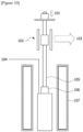
- a heat shrinkage rate was measured by a method of measuring length changes of a sample that appear while changing a temperature of 5°C under the conditions of 25°C to 120°C, using a TMA (thermomechanical analysis) apparatus under the trade name of Q400 manufactured by TA instruments.
- the heat shrinkage rate is based on length changes of the sample, where in Examples and Comparative Examples, the length change rate means a length change rate measured after being left at 120°C for 1 hour.
- the sample of the base layer was prepared so as to have an area of 600 mm x 300 mm and a thickness of 80 ⁇ m.
- the length change rate of the sample is measured by a thermal expansion coefficient meter (TMA).
- TMA thermal expansion coefficient meter
- the TMA is a measurement method that measures deformation of a sample appearing under a given load as a function of temperature and time when the sample has been heated or cooled to a given temperature condition.
- the force pressing the sample between the quartz stage and the probe which have little thermal deformation depending on temperatures, is 0.05 N, which is adjustable.
- the position change of the probe by the sample is measured by the electrical signal of the LVDT.
- L 0 is the length of the base layer in the MD direction at 25°C and L is the length of the base layer in the MD direction after heat treatment at 120°C for 1 hour.
- the heat shrinkable base layer is a PET (polyethylene terephthalate) film (SRF (super retardation film), manufactured by Toyobo) having an in-plane retardation value of 9000 nm for light having a wavelength of 550 nm and a thickness of 80 ⁇ m.
- SRF super retardation film
- ITO indium-tin-oxide
- a horizontal alignment film SE-7492, manufactured by Nissan Chemical Co., Ltd. was coated on the first electrode layer and the second electrode layer to a thickness of 300 ⁇ m, respectively, and cured to form first and second alignment films.
- An optical device was produced by applying a sealant to the outer periphery of the first alignment film, applying liquid crystals (MDA 14-4145, manufactured by Merck) to the inner area of the sealant and laminating the second alignment film thereto.
- the produced device has an area of 600 mm x 300 mm and a cell gap of 12 ⁇ m.
- An optical device was manufactured in the same manner as in Example 1, except that a TAC film (None, manufactured by FUJI) having a length change ratio of -0.01% in Evaluation Example 1 and a thickness of 80 ⁇ m was used as the first base layer and the second base layer, respectively.
- a TAC film Ni, manufactured by FUJI
- An optical device was manufactured in the same manner as in Example 1, except that a PC1 (polycarbonate) film (manufactured by Teigin) having a length change ratio of +0.15% in Evaluation Example 1 and a thickness of 100 ⁇ m was used as the first base layer and the second base layer, respectively.
- a PC1 (polycarbonate) film manufactured by Teigin having a length change ratio of +0.15% in Evaluation Example 1 and a thickness of 100 ⁇ m was used as the first base layer and the second base layer, respectively.
- An optical device was manufactured in the same manner as in Example 1, except that a PC2 (polycarbonate) film (manufactured by Keiwa) having a length change ratio of +0.16% in Evaluation Example 1 and a thickness of 100 ⁇ m was used as the first base layer and the second base layer, respectively.
- a PC2 (polycarbonate) film manufactured by Keiwa
- An optical device was manufactured in the same manner as in Example 1, except that a COP (cycloolefin copolymer) film (ZF14, manufactured by Zeon) having a length change ratio of +0.11% in Evaluation Example 1 and a thickness of 100 ⁇ m was used as the first base layer and the second base layer, respectively.
- a COP (cycloolefin copolymer) film ZF14, manufactured by Zeon
- optical devices of Examples and Comparative Examples were each subjected to a cycling test 10 times from a high temperature of 90°C to a low temperature of -40°C and then bubble occurrence was observed inside the optical device, and the results were shown in Table 1 below.
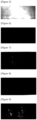
- the bubbles generated inside the optical device could also be observed with naked eyes, and the images photographing them with a digital camera were shown in Figures 4 to 9 .
- Figures 4 and 5 are images photographing the initial state of Example 1 before heat treatment and the state of Example 1 after 10 times of the cycling test, respectively, with a digital camera.
- Figures 6 and 7 are images photographing the initial state of Comparative Example 1 before heat treatment and the state of Comparative Example 1 after 10 times of the cycling test, respectively, with a digital camera.
- Figures 8 and 9 are images photographing the initial state of Comparative Example 2 before heat treatment and the state of Comparative Example 2 after 10 times of the cycling test, respectively, with a digital camera.
- Figures 4 and 5 in Example 1, no bubbles were observed with naked eyes even after the cycling test, but as shown in Figures 6 to 9 , in Comparative Examples 1 and 2, bubbles observed with naked eyes after the cycling test were generated.
- Example Comparative Example 1 2 1 2 3 Length change rate (%) -0.62 -0.01 0.15 0.16 0.11 Bubble occurrence X X O O O O O O: bubbles were observed with naked eyes; X: bubbles were not observed with naked eyes
- first base layer 20 liquid crystal layer 30: second base layer 40: sealant 101: load 102: LVDT (linear variable differential transformer) 103: signal related to position 104: thermocouple 105: probe 106: sample 107: furnace
Landscapes
- Physics & Mathematics (AREA)
- Chemical & Material Sciences (AREA)
- Nonlinear Science (AREA)
- Optics & Photonics (AREA)
- General Physics & Mathematics (AREA)
- Crystallography & Structural Chemistry (AREA)
- Mathematical Physics (AREA)
- Organic Chemistry (AREA)
- Health & Medical Sciences (AREA)
- Polymers & Plastics (AREA)
- Medicinal Chemistry (AREA)
- Chemical Kinetics & Catalysis (AREA)
- Engineering & Computer Science (AREA)
- Manufacturing & Machinery (AREA)
- Spectroscopy & Molecular Physics (AREA)
- Geometry (AREA)
- Materials Engineering (AREA)
- Liquid Crystal (AREA)
- Laminated Bodies (AREA)
- Polarising Elements (AREA)
Claims (10)
- Optische Vorrichtung, umfassend eine erste Basisschicht (10), eine Flüssig kristallschicht (20), eine zweite Basisschicht (30) der Reihe nach, eine erst e Elektrodenschicht, die auf der ersten Basisschicht (10) gebildet ist, und ei ne zweite Elektrodenschicht, die auf der zweiten Basisschicht (30) gebildet ist,wobei jede der ersten Basisschicht (10) und der zweiten Basisschicht (30) eine wärmeschrumpfbare Basisschicht ist,wobei die wärmeschrumpfbare Basisschicht eine Längenänderungsrate (ΔL) mit einer negativen Zahl in der folgenden Gleichung 1 aufweist:
 dadurch gekennzeichnet, dasswenn die wärmeschrumpfbare Basisschicht in einer MD-Richtung schrumpft, sie sich in einer TD-Richtung senkrecht zu der MD-Richtung mit einer Expansionsrate von 0,01-fach bis 0,5-fach einer Schrumpfungsrate in MD-Richtung expandiert, undwobei die optische Vorrichtung einen Überdruck aufweist, der höher als ein atmosphärischer Druck darin ist, wenn eine Temperatur von einer hohen Temperatur von 90 °C bis 100 °C auf eine niedrige Temperatur von -30 °C bis -40 °C geändert wird.
 - Optische Vorrichtung nach Anspruch 1, bei der die wärmeschrumpfbare Ba sisschicht einen Absolutwert einer Längenänderungsrate von 0,001% oder mehr aufweist.
- Optische Vorrichtung nach Anspruch 1, bei der die wärmeschrumpfbare Ba sisschicht einen Absolutwert einer Längenänderungsrate von 5% oder weni ger aufweist.
- Optische Vorrichtung nach Anspruch 1, bei der die wärmeschrumpfbare Ba sisschicht ein Verzögerungsfilm mit einem Verzögerungswert in der Ebene von 3000 nm oder mehr für Licht mit einer Wellenlänge von 550 nm ist.
- Optische Vorrichtung nach Anspruch 1, bei der die wärmeschrumpfbare Ba sisschicht ein Polyethylenterephthalat(PET)-Film oder ein Triacetylcellulos e(TAC)-Film ist.
- Optische Vorrichtung nach Anspruch 1, ferner umfassend einen ersten Aus richtungsfilm und einen zweiten Ausrichtungsfilm, die auf der ersten Elekt rodenschicht bzw. der zweiten Elektrodenschicht gebildet sind.
- Optische Vorrichtung nach Anspruch 1, bei der die Flüssigkristallschicht (2 o) dazu ausgelegt ist, zwischen einem transparenten Modus mit einer Durc hlässigkeit von 40% oder mehr und einem nicht transparenten Modus mit einer Durchlässigkeit von weniger als 40% in Abhängigkeit von einer angel egten Spannung umzuschalten.
- Optische Vorrichtung nach Anspruch 1, bei der die Flüssigkristallschicht (2 o) eine smektische Flüssigkristallverbindung, eine nematische Flüssigkrist allverbindung oder eine cholesterische Flüssigkristallverbindung umfasst.
- Optische Vorrichtung nach Anspruch 1, bei der die Flüssigkristallschicht fe rner einen anisotropen Farbstoff umfasst.
- Optische Vorrichtung nach Anspruch 1, bei der die Flüssigkristallschicht fe rner ein Dichtmittel (40) auf ihren Seiten umfasst.
Applications Claiming Priority (2)
| Application Number | Priority Date | Filing Date | Title |
|---|---|---|---|
| KR1020180048684A KR102183677B1 (ko) | 2018-04-26 | 2018-04-26 | 광학 디바이스 및 이의 용도 |
| PCT/KR2019/004967 WO2019209029A1 (ko) | 2018-04-26 | 2019-04-24 | 광학 디바이스 및 이의 용도 |
Publications (3)
| Publication Number | Publication Date |
|---|---|
| EP3786697A1 EP3786697A1 (de) | 2021-03-03 |
| EP3786697A4 EP3786697A4 (de) | 2021-06-09 |
| EP3786697B1 true EP3786697B1 (de) | 2025-02-26 |
Family
ID=68294162
Family Applications (1)
| Application Number | Title | Priority Date | Filing Date |
|---|---|---|---|
| EP19792177.8A Active EP3786697B1 (de) | 2018-04-26 | 2019-04-24 | Optische vorrichtung und verwendung davon |
Country Status (6)
| Country | Link |
|---|---|
| US (1) | US11428968B2 (de) |
| EP (1) | EP3786697B1 (de) |
| JP (1) | JP7102543B2 (de) |
| KR (1) | KR102183677B1 (de) |
| CN (1) | CN111936921B (de) |
| WO (1) | WO2019209029A1 (de) |
Families Citing this family (3)
| Publication number | Priority date | Publication date | Assignee | Title |
|---|---|---|---|---|
| KR102799955B1 (ko) | 2019-10-08 | 2025-04-25 | 주식회사 엘지에너지솔루션 | 물리적 결합으로 전극리드와 연결되는 연결부재, 및 이를 포함하는 전지셀 스택 |
| GB202018219D0 (en) | 2020-11-19 | 2021-01-06 | Pilkington Group Ltd | Film |
| KR102628860B1 (ko) | 2022-06-07 | 2024-01-25 | 동우 화인켐 주식회사 | 광학 적층체 및 이의 제조방법과, 이를 포함하는 스마트 윈도우 |
Citations (1)
| Publication number | Priority date | Publication date | Assignee | Title |
|---|---|---|---|---|
| US4586790A (en) * | 1982-02-22 | 1986-05-06 | Hitachi, Ltd. | Display panel having uniaxially-stretched organic polymer film as the substrate |
Family Cites Families (24)
| Publication number | Priority date | Publication date | Assignee | Title |
|---|---|---|---|---|
| JPS5988719A (ja) | 1982-11-15 | 1984-05-22 | Diafoil Co Ltd | 液晶パネル基材用ポリエステルフイルム |
| JPS60170829A (ja) * | 1984-02-15 | 1985-09-04 | Canon Inc | 液晶パネル |
| JPS6151323A (ja) * | 1984-08-22 | 1986-03-13 | Toray Ind Inc | 液晶表示用一軸伸ポリエステルフイルムの製造方法 |
| JPH0543130U (ja) | 1991-11-05 | 1993-06-11 | 株式会社東芝 | カラー液晶表示器 |
| JP3773723B2 (ja) * | 1999-01-29 | 2006-05-10 | シャープ株式会社 | 液晶表示装置 |
| JP2001142055A (ja) * | 1999-11-12 | 2001-05-25 | Ricoh Co Ltd | 液晶素子とその製造方法 |
| JP2002258255A (ja) * | 2001-03-02 | 2002-09-11 | Matsushita Electric Ind Co Ltd | プラスチック基板を用いた液晶表示装置 |
| FR2857467B1 (fr) | 2003-07-09 | 2005-08-19 | Saint Gobain | Dispositif electrocommandable a proprietes optiques et/ou energetiques variables |
| JP2006133720A (ja) * | 2004-10-07 | 2006-05-25 | Nitto Denko Corp | 複屈折フィルムの製造方法、およびそれを用いた光学フィルム、液晶パネル、液晶表示装置、画像表示装置 |
| US8105458B2 (en) * | 2007-03-23 | 2012-01-31 | Semiconductor Energy Laboratory Co., Ltd. | Method for manufacturing liquid crystal display device |
| JP2009098667A (ja) * | 2007-09-28 | 2009-05-07 | Fujifilm Corp | 液晶表示装置 |
| KR102065116B1 (ko) | 2011-07-14 | 2020-01-10 | 삼성전자주식회사 | 광 투과량 조절 소자, 이를 포함한 영상 기기 및 그 제조 방법 |
| JP6286864B2 (ja) * | 2013-05-14 | 2018-03-07 | 東洋紡株式会社 | ガスバリア性フィルム |
| US10074760B2 (en) * | 2014-03-24 | 2018-09-11 | Toray Industries, Inc. | Solar cell back sheet and solar cell module |
| CN106233364B (zh) | 2014-04-28 | 2019-07-12 | 夏普株式会社 | 反射镜显示器 |
| CN104360544B (zh) * | 2014-11-14 | 2017-07-14 | 京东方科技集团股份有限公司 | 液晶盒组件及其制作方法、液晶显示面板和显示设备 |
| US20160170118A1 (en) * | 2014-12-15 | 2016-06-16 | Kent State University | Active retardation films based on polymer stabilized cholesteric liquid crystal |
| JP6674463B2 (ja) * | 2015-07-23 | 2020-04-01 | 富士フイルム株式会社 | 液晶セル、3次元構造液晶セル前駆体、および、3次元構造液晶セルの製造方法 |
| KR102114562B1 (ko) | 2015-08-11 | 2020-05-26 | 노파르티스 아게 | 암의 치료에 사용하기 위한 5-브로모-2,6-디-(1h-피라졸-1-일)피리미딘-4-아민 |
| JP2017090555A (ja) * | 2015-11-04 | 2017-05-25 | パナソニック液晶ディスプレイ株式会社 | 液晶表示装置、液晶表示装置の製造方法、及び表示装置の製造方法 |
| KR102258279B1 (ko) | 2015-12-02 | 2021-05-31 | 주식회사 엘지화학 | 광학 소자 |
| JP2017151289A (ja) | 2016-02-25 | 2017-08-31 | 株式会社ジャパンディスプレイ | 熱硬化性シール材、表示装置及び表示装置の製造方法 |
| JP6641587B2 (ja) | 2016-07-27 | 2020-02-05 | エルジー・ケム・リミテッド | 透過度可変フィルム、その製造方法および用途 |
| KR102040293B1 (ko) * | 2016-08-29 | 2019-11-04 | 삼성에스디아이 주식회사 | 액정표시장치 |
-
2018
- 2018-04-26 KR KR1020180048684A patent/KR102183677B1/ko active Active
-
2019
- 2019-04-24 EP EP19792177.8A patent/EP3786697B1/de active Active
- 2019-04-24 CN CN201980024046.8A patent/CN111936921B/zh active Active
- 2019-04-24 US US17/046,165 patent/US11428968B2/en active Active
- 2019-04-24 WO PCT/KR2019/004967 patent/WO2019209029A1/ko not_active Ceased
- 2019-04-24 JP JP2020552233A patent/JP7102543B2/ja active Active
Patent Citations (1)
| Publication number | Priority date | Publication date | Assignee | Title |
|---|---|---|---|---|
| US4586790A (en) * | 1982-02-22 | 1986-05-06 | Hitachi, Ltd. | Display panel having uniaxially-stretched organic polymer film as the substrate |
Also Published As
| Publication number | Publication date |
|---|---|
| EP3786697A1 (de) | 2021-03-03 |
| KR20190124560A (ko) | 2019-11-05 |
| WO2019209029A1 (ko) | 2019-10-31 |
| JP7102543B2 (ja) | 2022-07-19 |
| CN111936921B (zh) | 2023-06-02 |
| CN111936921A (zh) | 2020-11-13 |
| KR102183677B1 (ko) | 2020-11-27 |
| JP2021517991A (ja) | 2021-07-29 |
| EP3786697A4 (de) | 2021-06-09 |
| US20210157196A1 (en) | 2021-05-27 |
| US11428968B2 (en) | 2022-08-30 |
Similar Documents
| Publication | Publication Date | Title |
|---|---|---|
| KR100300168B1 (ko) | 액정표시장치 | |
| CN100397203C (zh) | 包括使用正双轴延迟膜的视角补偿膜的面内切换液晶显示器 | |
| JP3926072B2 (ja) | 液晶表示装置 | |
| JP5000729B2 (ja) | 液晶表示装置の製造方法、及び、液晶表示装置 | |
| KR100717564B1 (ko) | 액정 표시 장치 | |
| EP2693243B1 (de) | Integrierte O-Folie zur Verbesserung des Ansichtswinkels einer TN-LCD sowie Polarisationsplatte und TN-LCD damit | |
| US20140184988A1 (en) | Optical film, polarizing plate, liquid crystal display, and method of manufacturing optical film | |
| JP4801363B2 (ja) | 液晶表示素子 | |
| JP2000019518A (ja) | 液晶表示装置 | |
| EP3786697B1 (de) | Optische vorrichtung und verwendung davon | |
| KR20050101743A (ko) | 광학 필름 | |
| US6888598B2 (en) | Optical film and liquid crystal display device having optical film | |
| KR100304226B1 (ko) | 액정표시장치 | |
| US20150185559A1 (en) | Optical film, method for manufacturing same, and liquid crystal display including same | |
| KR100672656B1 (ko) | 액정표시장치 | |
| KR101565009B1 (ko) | 하판 편광판 및 이를 포함하는 면상 스위칭 모드 액정표시장치 | |
| JP3830456B2 (ja) | 液晶表示装置 | |
| KR20100064522A (ko) | 상판 편광판 및 이를 포함하는 면상 스위칭 모드 액정표시장치 | |
| WO2009072815A9 (en) | Integrated wide viewing film and in-plan switching liquid crystal display with the same | |
| KR100502812B1 (ko) | 위상차 보상막을 이용한 광시야각 액정 표시 장치 | |
| CN120390893A (zh) | 层叠体、液晶显示装置及车载显示器 | |
| JP3452481B2 (ja) | 液晶表示装置 | |
| JP2004341561A (ja) | 液晶表示装置 | |
| JPH1073799A (ja) | 液晶表示素子 | |
| KR20200105215A (ko) | 편광판 |
Legal Events
| Date | Code | Title | Description |
|---|---|---|---|
| STAA | Information on the status of an ep patent application or granted ep patent |
Free format text: STATUS: THE INTERNATIONAL PUBLICATION HAS BEEN MADE |
|
| PUAI | Public reference made under article 153(3) epc to a published international application that has entered the european phase |
Free format text: ORIGINAL CODE: 0009012 |
|
| STAA | Information on the status of an ep patent application or granted ep patent |
Free format text: STATUS: REQUEST FOR EXAMINATION WAS MADE |
|
| 17P | Request for examination filed |
Effective date: 20200925 |
|
| AK | Designated contracting states |
Kind code of ref document: A1 Designated state(s): AL AT BE BG CH CY CZ DE DK EE ES FI FR GB GR HR HU IE IS IT LI LT LU LV MC MK MT NL NO PL PT RO RS SE SI SK SM TR |
|
| AX | Request for extension of the european patent |
Extension state: BA ME |
|
| A4 | Supplementary search report drawn up and despatched |
Effective date: 20210507 |
|
| RIC1 | Information provided on ipc code assigned before grant |
Ipc: G02F 1/13363 20060101AFI20210430BHEP Ipc: G02F 1/13 20060101ALI20210430BHEP Ipc: C08J 5/18 20060101ALI20210430BHEP Ipc: C08L 1/12 20060101ALI20210430BHEP Ipc: C08L 67/02 20060101ALI20210430BHEP |
|
| DAV | Request for validation of the european patent (deleted) | ||
| DAX | Request for extension of the european patent (deleted) | ||
| STAA | Information on the status of an ep patent application or granted ep patent |
Free format text: STATUS: EXAMINATION IS IN PROGRESS |
|
| 17Q | First examination report despatched |
Effective date: 20230523 |
|
| GRAP | Despatch of communication of intention to grant a patent |
Free format text: ORIGINAL CODE: EPIDOSNIGR1 |
|
| STAA | Information on the status of an ep patent application or granted ep patent |
Free format text: STATUS: GRANT OF PATENT IS INTENDED |
|
| INTG | Intention to grant announced |
Effective date: 20241016 |
|
| GRAS | Grant fee paid |
Free format text: ORIGINAL CODE: EPIDOSNIGR3 |
|
| GRAA | (expected) grant |
Free format text: ORIGINAL CODE: 0009210 |
|
| STAA | Information on the status of an ep patent application or granted ep patent |
Free format text: STATUS: THE PATENT HAS BEEN GRANTED |
|
| AK | Designated contracting states |
Kind code of ref document: B1 Designated state(s): AL AT BE BG CH CY CZ DE DK EE ES FI FR GB GR HR HU IE IS IT LI LT LU LV MC MK MT NL NO PL PT RO RS SE SI SK SM TR |
|
| REG | Reference to a national code |
Ref country code: GB Ref legal event code: FG4D |
|
| REG | Reference to a national code |
Ref country code: CH Ref legal event code: EP |
|
| REG | Reference to a national code |
Ref country code: DE Ref legal event code: R096 Ref document number: 602019066540 Country of ref document: DE |
|
| REG | Reference to a national code |
Ref country code: IE Ref legal event code: FG4D |
|
| PGFP | Annual fee paid to national office [announced via postgrant information from national office to epo] |
Ref country code: FR Payment date: 20250321 Year of fee payment: 7 |
|
| PGFP | Annual fee paid to national office [announced via postgrant information from national office to epo] |
Ref country code: GB Payment date: 20250320 Year of fee payment: 7 |
|
| REG | Reference to a national code |
Ref country code: NL Ref legal event code: MP Effective date: 20250226 |
|
| PG25 | Lapsed in a contracting state [announced via postgrant information from national office to epo] |
Ref country code: RS Free format text: LAPSE BECAUSE OF FAILURE TO SUBMIT A TRANSLATION OF THE DESCRIPTION OR TO PAY THE FEE WITHIN THE PRESCRIBED TIME-LIMIT Effective date: 20250526 |
|
| PG25 | Lapsed in a contracting state [announced via postgrant information from national office to epo] |
Ref country code: FI Free format text: LAPSE BECAUSE OF FAILURE TO SUBMIT A TRANSLATION OF THE DESCRIPTION OR TO PAY THE FEE WITHIN THE PRESCRIBED TIME-LIMIT Effective date: 20250226 |
|
| PG25 | Lapsed in a contracting state [announced via postgrant information from national office to epo] |
Ref country code: PL Free format text: LAPSE BECAUSE OF FAILURE TO SUBMIT A TRANSLATION OF THE DESCRIPTION OR TO PAY THE FEE WITHIN THE PRESCRIBED TIME-LIMIT Effective date: 20250226 |
|
| PGFP | Annual fee paid to national office [announced via postgrant information from national office to epo] |
Ref country code: DE Payment date: 20250320 Year of fee payment: 7 |
|
| PG25 | Lapsed in a contracting state [announced via postgrant information from national office to epo] |
Ref country code: ES Free format text: LAPSE BECAUSE OF FAILURE TO SUBMIT A TRANSLATION OF THE DESCRIPTION OR TO PAY THE FEE WITHIN THE PRESCRIBED TIME-LIMIT Effective date: 20250226 |
|
| REG | Reference to a national code |
Ref country code: LT Ref legal event code: MG9D |
|
| PG25 | Lapsed in a contracting state [announced via postgrant information from national office to epo] |
Ref country code: NO Free format text: LAPSE BECAUSE OF FAILURE TO SUBMIT A TRANSLATION OF THE DESCRIPTION OR TO PAY THE FEE WITHIN THE PRESCRIBED TIME-LIMIT Effective date: 20250526 Ref country code: IS Free format text: LAPSE BECAUSE OF FAILURE TO SUBMIT A TRANSLATION OF THE DESCRIPTION OR TO PAY THE FEE WITHIN THE PRESCRIBED TIME-LIMIT Effective date: 20250626 |
|
| PG25 | Lapsed in a contracting state [announced via postgrant information from national office to epo] |
Ref country code: NL Free format text: LAPSE BECAUSE OF FAILURE TO SUBMIT A TRANSLATION OF THE DESCRIPTION OR TO PAY THE FEE WITHIN THE PRESCRIBED TIME-LIMIT Effective date: 20250226 |
|
| PG25 | Lapsed in a contracting state [announced via postgrant information from national office to epo] |
Ref country code: HR Free format text: LAPSE BECAUSE OF FAILURE TO SUBMIT A TRANSLATION OF THE DESCRIPTION OR TO PAY THE FEE WITHIN THE PRESCRIBED TIME-LIMIT Effective date: 20250226 |
|
| PG25 | Lapsed in a contracting state [announced via postgrant information from national office to epo] |
Ref country code: PT Free format text: LAPSE BECAUSE OF FAILURE TO SUBMIT A TRANSLATION OF THE DESCRIPTION OR TO PAY THE FEE WITHIN THE PRESCRIBED TIME-LIMIT Effective date: 20250626 Ref country code: LV Free format text: LAPSE BECAUSE OF FAILURE TO SUBMIT A TRANSLATION OF THE DESCRIPTION OR TO PAY THE FEE WITHIN THE PRESCRIBED TIME-LIMIT Effective date: 20250226 |
|
| PG25 | Lapsed in a contracting state [announced via postgrant information from national office to epo] |
Ref country code: GR Free format text: LAPSE BECAUSE OF FAILURE TO SUBMIT A TRANSLATION OF THE DESCRIPTION OR TO PAY THE FEE WITHIN THE PRESCRIBED TIME-LIMIT Effective date: 20250527 Ref country code: BG Free format text: LAPSE BECAUSE OF FAILURE TO SUBMIT A TRANSLATION OF THE DESCRIPTION OR TO PAY THE FEE WITHIN THE PRESCRIBED TIME-LIMIT Effective date: 20250226 |
|
| REG | Reference to a national code |
Ref country code: AT Ref legal event code: MK05 Ref document number: 1771208 Country of ref document: AT Kind code of ref document: T Effective date: 20250226 |
|
| PG25 | Lapsed in a contracting state [announced via postgrant information from national office to epo] |
Ref country code: SE Free format text: LAPSE BECAUSE OF FAILURE TO SUBMIT A TRANSLATION OF THE DESCRIPTION OR TO PAY THE FEE WITHIN THE PRESCRIBED TIME-LIMIT Effective date: 20250226 |
|
| PG25 | Lapsed in a contracting state [announced via postgrant information from national office to epo] |
Ref country code: SM Free format text: LAPSE BECAUSE OF FAILURE TO SUBMIT A TRANSLATION OF THE DESCRIPTION OR TO PAY THE FEE WITHIN THE PRESCRIBED TIME-LIMIT Effective date: 20250226 |
|
| PG25 | Lapsed in a contracting state [announced via postgrant information from national office to epo] |
Ref country code: DK Free format text: LAPSE BECAUSE OF FAILURE TO SUBMIT A TRANSLATION OF THE DESCRIPTION OR TO PAY THE FEE WITHIN THE PRESCRIBED TIME-LIMIT Effective date: 20250226 |
|
| PG25 | Lapsed in a contracting state [announced via postgrant information from national office to epo] |
Ref country code: IT Free format text: LAPSE BECAUSE OF FAILURE TO SUBMIT A TRANSLATION OF THE DESCRIPTION OR TO PAY THE FEE WITHIN THE PRESCRIBED TIME-LIMIT Effective date: 20250226 |
|
| PG25 | Lapsed in a contracting state [announced via postgrant information from national office to epo] |
Ref country code: AT Free format text: LAPSE BECAUSE OF FAILURE TO SUBMIT A TRANSLATION OF THE DESCRIPTION OR TO PAY THE FEE WITHIN THE PRESCRIBED TIME-LIMIT Effective date: 20250226 |
|
| PG25 | Lapsed in a contracting state [announced via postgrant information from national office to epo] |
Ref country code: EE Free format text: LAPSE BECAUSE OF FAILURE TO SUBMIT A TRANSLATION OF THE DESCRIPTION OR TO PAY THE FEE WITHIN THE PRESCRIBED TIME-LIMIT Effective date: 20250226 Ref country code: CZ Free format text: LAPSE BECAUSE OF FAILURE TO SUBMIT A TRANSLATION OF THE DESCRIPTION OR TO PAY THE FEE WITHIN THE PRESCRIBED TIME-LIMIT Effective date: 20250226 |
|
| PG25 | Lapsed in a contracting state [announced via postgrant information from national office to epo] |
Ref country code: RO Free format text: LAPSE BECAUSE OF FAILURE TO SUBMIT A TRANSLATION OF THE DESCRIPTION OR TO PAY THE FEE WITHIN THE PRESCRIBED TIME-LIMIT Effective date: 20250226 |
|
| PG25 | Lapsed in a contracting state [announced via postgrant information from national office to epo] |
Ref country code: SK Free format text: LAPSE BECAUSE OF FAILURE TO SUBMIT A TRANSLATION OF THE DESCRIPTION OR TO PAY THE FEE WITHIN THE PRESCRIBED TIME-LIMIT Effective date: 20250226 |
|
| REG | Reference to a national code |
Ref country code: CH Ref legal event code: H13 Free format text: ST27 STATUS EVENT CODE: U-0-0-H10-H13 (AS PROVIDED BY THE NATIONAL OFFICE) Effective date: 20251125 |
|
| REG | Reference to a national code |
Ref country code: DE Ref legal event code: R097 Ref document number: 602019066540 Country of ref document: DE |
|
| PG25 | Lapsed in a contracting state [announced via postgrant information from national office to epo] |
Ref country code: LU Free format text: LAPSE BECAUSE OF NON-PAYMENT OF DUE FEES Effective date: 20250424 |
|
| PG25 | Lapsed in a contracting state [announced via postgrant information from national office to epo] |
Ref country code: MC Free format text: LAPSE BECAUSE OF FAILURE TO SUBMIT A TRANSLATION OF THE DESCRIPTION OR TO PAY THE FEE WITHIN THE PRESCRIBED TIME-LIMIT Effective date: 20250226 |
|
| REG | Reference to a national code |
Ref country code: BE Ref legal event code: MM Effective date: 20250430 |
|
| PLBE | No opposition filed within time limit |
Free format text: ORIGINAL CODE: 0009261 |
|
| STAA | Information on the status of an ep patent application or granted ep patent |
Free format text: STATUS: NO OPPOSITION FILED WITHIN TIME LIMIT |
|
| PG25 | Lapsed in a contracting state [announced via postgrant information from national office to epo] |
Ref country code: BE Free format text: LAPSE BECAUSE OF NON-PAYMENT OF DUE FEES Effective date: 20250430 |
|
| PG25 | Lapsed in a contracting state [announced via postgrant information from national office to epo] |
Ref country code: CH Free format text: LAPSE BECAUSE OF NON-PAYMENT OF DUE FEES Effective date: 20250430 |
|
| 26N | No opposition filed |
Effective date: 20251127 |