EP3780368A1 - Stromversorgungsschaltung und -vorrichtung - Google Patents
Stromversorgungsschaltung und -vorrichtung Download PDFInfo
- Publication number
- EP3780368A1 EP3780368A1 EP18916536.8A EP18916536A EP3780368A1 EP 3780368 A1 EP3780368 A1 EP 3780368A1 EP 18916536 A EP18916536 A EP 18916536A EP 3780368 A1 EP3780368 A1 EP 3780368A1
- Authority
- EP
- European Patent Office
- Prior art keywords
- switching transistor
- capacitor
- electrode
- power supply
- transistor
- Prior art date
- Legal status (The legal status is an assumption and is not a legal conclusion. Google has not performed a legal analysis and makes no representation as to the accuracy of the status listed.)
- Granted
Links
Images
Classifications
-
- H—ELECTRICITY
- H03—ELECTRONIC CIRCUITRY
- H03K—PULSE TECHNIQUE
- H03K17/00—Electronic switching or gating, i.e. not by contact-making and –breaking
- H03K17/04—Modifications for accelerating switching
- H03K17/041—Modifications for accelerating switching without feedback from the output circuit to the control circuit
- H03K17/0412—Modifications for accelerating switching without feedback from the output circuit to the control circuit by measures taken in the control circuit
- H03K17/04123—Modifications for accelerating switching without feedback from the output circuit to the control circuit by measures taken in the control circuit in field-effect transistor switches
-
- H—ELECTRICITY
- H03—ELECTRONIC CIRCUITRY
- H03K—PULSE TECHNIQUE
- H03K17/00—Electronic switching or gating, i.e. not by contact-making and –breaking
- H03K17/51—Electronic switching or gating, i.e. not by contact-making and –breaking characterised by the components used
- H03K17/56—Electronic switching or gating, i.e. not by contact-making and –breaking characterised by the components used by the use, as active elements, of semiconductor devices
- H03K17/687—Electronic switching or gating, i.e. not by contact-making and –breaking characterised by the components used by the use, as active elements, of semiconductor devices the devices being field-effect transistors
- H03K17/693—Switching arrangements with several input- or output-terminals, e.g. multiplexers, distributors
-
- G—PHYSICS
- G05—CONTROLLING; REGULATING
- G05F—SYSTEMS FOR REGULATING ELECTRIC OR MAGNETIC VARIABLES
- G05F1/00—Automatic systems in which deviations of an electric quantity from one or more predetermined values are detected at the output of the system and fed back to a device within the system to restore the detected quantity to its predetermined value or values, i.e. retroactive systems
- G05F1/10—Regulating voltage or current
- G05F1/46—Regulating voltage or current wherein the variable actually regulated by the final control device is DC
-
- H—ELECTRICITY
- H01—ELECTRIC ELEMENTS
- H01G—CAPACITORS; CAPACITORS, RECTIFIERS, DETECTORS, SWITCHING DEVICES, LIGHT-SENSITIVE OR TEMPERATURE-SENSITIVE DEVICES OF THE ELECTROLYTIC TYPE
- H01G9/00—Electrolytic capacitors, rectifiers, detectors, switching devices, light-sensitive or temperature-sensitive devices; Processes of their manufacture
- H01G9/004—Details
- H01G9/008—Terminals
-
- H—ELECTRICITY
- H02—GENERATION; CONVERSION OR DISTRIBUTION OF ELECTRIC POWER
- H02M—APPARATUS FOR CONVERSION BETWEEN AC AND AC, BETWEEN AC AND DC, OR BETWEEN DC AND DC, AND FOR USE WITH MAINS OR SIMILAR POWER SUPPLY SYSTEMS; CONVERSION OF DC OR AC INPUT POWER INTO SURGE OUTPUT POWER; CONTROL OR REGULATION THEREOF
- H02M3/00—Conversion of DC power input into DC power output
- H02M3/02—Conversion of DC power input into DC power output without intermediate conversion into AC
- H02M3/04—Conversion of DC power input into DC power output without intermediate conversion into AC by static converters
- H02M3/10—Conversion of DC power input into DC power output without intermediate conversion into AC by static converters using discharge tubes with control electrode or semiconductor devices with control electrode
- H02M3/145—Conversion of DC power input into DC power output without intermediate conversion into AC by static converters using discharge tubes with control electrode or semiconductor devices with control electrode using devices of a triode or transistor type requiring continuous application of a control signal
- H02M3/155—Conversion of DC power input into DC power output without intermediate conversion into AC by static converters using discharge tubes with control electrode or semiconductor devices with control electrode using devices of a triode or transistor type requiring continuous application of a control signal using semiconductor devices only
- H02M3/156—Conversion of DC power input into DC power output without intermediate conversion into AC by static converters using discharge tubes with control electrode or semiconductor devices with control electrode using devices of a triode or transistor type requiring continuous application of a control signal using semiconductor devices only with automatic control of output voltage or current, e.g. switching regulators
-
- H—ELECTRICITY
- H02—GENERATION; CONVERSION OR DISTRIBUTION OF ELECTRIC POWER
- H02M—APPARATUS FOR CONVERSION BETWEEN AC AND AC, BETWEEN AC AND DC, OR BETWEEN DC AND DC, AND FOR USE WITH MAINS OR SIMILAR POWER SUPPLY SYSTEMS; CONVERSION OF DC OR AC INPUT POWER INTO SURGE OUTPUT POWER; CONTROL OR REGULATION THEREOF
- H02M3/00—Conversion of DC power input into DC power output
- H02M3/22—Conversion of DC power input into DC power output with intermediate conversion into AC
- H02M3/24—Conversion of DC power input into DC power output with intermediate conversion into AC by static converters
- H02M3/28—Conversion of DC power input into DC power output with intermediate conversion into AC by static converters using discharge tubes with control electrode or semiconductor devices with control electrode to produce the intermediate AC
- H02M3/325—Conversion of DC power input into DC power output with intermediate conversion into AC by static converters using discharge tubes with control electrode or semiconductor devices with control electrode to produce the intermediate AC using devices of a triode or a transistor type requiring continuous application of a control signal
- H02M3/335—Conversion of DC power input into DC power output with intermediate conversion into AC by static converters using discharge tubes with control electrode or semiconductor devices with control electrode to produce the intermediate AC using devices of a triode or a transistor type requiring continuous application of a control signal using semiconductor devices only
-
- H—ELECTRICITY
- H03—ELECTRONIC CIRCUITRY
- H03F—AMPLIFIERS
- H03F3/00—Amplifiers with only discharge tubes or only semiconductor devices as amplifying elements
- H03F3/20—Power amplifiers, e.g. Class B amplifiers, Class C amplifiers
- H03F3/24—Power amplifiers, e.g. Class B amplifiers, Class C amplifiers of transmitter output stages
- H03F3/245—Power amplifiers, e.g. Class B amplifiers, Class C amplifiers of transmitter output stages with semiconductor devices only
-
- H—ELECTRICITY
- H03—ELECTRONIC CIRCUITRY
- H03K—PULSE TECHNIQUE
- H03K17/00—Electronic switching or gating, i.e. not by contact-making and –breaking
- H03K17/04—Modifications for accelerating switching
- H03K17/041—Modifications for accelerating switching without feedback from the output circuit to the control circuit
- H03K17/04106—Modifications for accelerating switching without feedback from the output circuit to the control circuit in field-effect transistor switches
-
- H—ELECTRICITY
- H03—ELECTRONIC CIRCUITRY
- H03F—AMPLIFIERS
- H03F2200/00—Indexing scheme relating to amplifiers
- H03F2200/102—A non-specified detector of a signal envelope being used in an amplifying circuit
-
- H—ELECTRICITY
- H03—ELECTRONIC CIRCUITRY
- H03K—PULSE TECHNIQUE
- H03K2217/00—Indexing scheme related to electronic switching or gating, i.e. not by contact-making or -breaking covered by H03K17/00
- H03K2217/0063—High side switches, i.e. the higher potential [DC] or life wire [AC] being directly connected to the switch and not via the load
-
- H—ELECTRICITY
- H03—ELECTRONIC CIRCUITRY
- H03K—PULSE TECHNIQUE
- H03K2217/00—Indexing scheme related to electronic switching or gating, i.e. not by contact-making or -breaking covered by H03K17/00
- H03K2217/0081—Power supply means, e.g. to the switch driver
Definitions
- This application relates to the field of electronic technologies, and in particular, to a power supply circuit and an apparatus.
- a complex variable envelope modulation scheme is widely used in a new generation wireless communications system, so that a modulation signal has a very high peak-to-average power ratio (Peak-to-Average Power Ratio, PAPR).
- An envelope tracking (Envelope Tracking, ET) technology may be used to effectively resolve a problem that a power amplifier has low efficiency when a modulation signal with a high PAPR is input, and has a broad application prospect.
- a core of the ET technology includes the following: extracting an envelope of a radio frequency signal, and using the envelope as a reference for a power supply of a radio frequency power amplifier, so that the power supply of the radio frequency power amplifier changes with the envelope, and the power amplifier can always operate in a saturation region.
- a tracking bandwidth is a key element of an envelope tracking power supply. If a switching converter has a higher switching frequency, a higher tracking bandwidth of the converter can be implemented. However, due to limitation of performance of a switching component, an excessively high switching frequency increases switching losses and reduces efficiency of the switching converter, and consequently causes low dynamic performance of a circuit system.
- This application provides a power supply circuit and an apparatus, to improve stability of a circuit system and dynamic performance of the circuit system.
- an embodiment of this application provides a circuit, where the circuit includes a plurality of channels, and at least one channel or each channel of the plurality of channels includes a first switching transistor, a second switching transistor, a third switching transistor, a fourth switching transistor, a first capacitor, and a second capacitor; one terminal of the first capacitor is connected to one terminal of the second capacitor, the other terminal of the first capacitor is connected to each of a first electrode of the first switching transistor and a first electrode of the second switching transistor, a second electrode of the first switching transistor is connected to a second electrode of the third switching transistor, a second electrode of the second switching transistor is connected to a second electrode of the fourth switching transistor, a third electrode of the first switching transistor is connected to an output node, and a third electrode of the second switching transistor is grounded.
- Charging charges of the second capacitor are balanced by using an ideal charge storage capacity of the first capacitor. This improves stability of a circuit system and dynamic performance of the circuit system.
- the first switching transistor M1' is turned on, the second switching transistor M2' is turned off, a lower plate of the first capacitor C1' is connected to the output node VSSH, a potential of the lower plate is also equal to the potential of the VDD, and the potentials of the lower plates of the first capacitor C1' and the second capacitor C1 are equal.
- the ideal charge storage capacity of the first capacitor C1' may be used to balance the charging charges of the second capacitor C1.
- the third switching transistor M1 when the third switching transistor M1 is turned off and the fourth switching transistor M2 is turned on, a potential of the output node VSSH does not deviate from a potential of the voltage source source of lowside VSSL.
- the third switching transistor M1 when the third switching transistor M1 is turned on and the fourth switching transistor M2 is turned off, a potential of the output node VSSH does not deviate from the potential of the VDD, to avoid voltage fluctuation and provide a buffer function for the second capacitor C1.
- a type of the first switching transistor M1' is the same as a type of the third switching transistor M1, to ensure that the first switching transistor M1' and the third switching transistor M1 are both turned off or turned on when a same drive signal is input.
- a type of the second switching transistor M2' is the same as a type of the fourth switching transistor M2, to ensure that the second switching transistor M2' and the fourth switching transistor M2 are both turned off or turned on when a same drive signal is input.
- a size of the first switching transistor M1' is X times a size of the third switching transistor M1
- a size of the second switching transistor M2' is Y times a size of the fourth switching transistor M2
- both X and Y are greater than 1. Because a larger size of a switching transistor indicates smaller impedance and a better heat dissipation effect, a first switching transistor M1' and a second switching transistor M2' of sizes as large as possible can be selected.
- the first switching transistor M1' and the second switching transistor M2' are selected based on an actual signal frequency. Because a smaller signal frequency indicates larger impedance, a first switching transistor M1' of a relatively large size and a second switching transistor M2' of a relatively large size can be selected. Because a larger signal frequency indicates smaller impedance, a first switching transistor M1' of a relatively small size and a second switching transistor M2' of a relatively small size can be selected.
- the first switching transistor M1', the second switching transistor M2', the third switching transistor M1, or the fourth switching transistor M2 includes but is not limited to a bipolar transistor, a metal-oxide semiconductor field-effect transistor, or various III-V compound semiconductors.
- the first capacitor C1' or the second capacitor C1 may include but is not limited to a ceramic capacitor, a tantalum capacitor, or an electrolytic capacitor.
- the power supply circuit is a multi-phase modulation power supply circuit.
- an embodiment of this application discloses a power supply circuit, where the circuit includes a plurality of channels, and each channel or at least one channel of the plurality of channels includes a first switching transistor, a second switching transistor, a first capacitor, and a power supply chip, the power supply chip includes a third switching transistor, a fourth switching transistor, and a second capacitor; one terminal of the first capacitor is connected to one terminal of the second capacitor, the other terminal of the first capacitor is connected to each of a first electrode of the first switching transistor and a first electrode of the second switching transistor, a second electrode of the first switching transistor is connected to a second electrode of the third switching transistor, a second electrode of the second switching transistor is connected to a second electrode of the fourth switching transistor, a third electrode of the first switching transistor is connected to an output node, and a third electrode of the second switching transistor is grounded.
- Charging charges of the second capacitor are balanced by using an ideal charge storage capacity of the first capacitor. This improves stability of a circuit system and dynamic performance of the circuit system.
- the first capacitor C1' may be disposed inside the power supply chip, thereby facilitating integration of the power supply chip and reducing power consumption of the circuit.
- the first capacitor C1' may be disposed outside the power supply chip, thereby facilitating selection of a capacitor with a larger capacitance, and achieving a better effect of improving stability of the circuit.
- the first capacitor C1' may be disposed adjacent to the second capacitor.
- the first switching transistor M1' and the second switching transistor M2' may be disposed outside the power supply chip, or may be disposed inside the power supply chip.
- an embodiment of this application provides an apparatus, where the apparatus includes either of the power supply circuits provided in the first aspect and the second aspect.
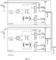
- FIG. 1 is a schematic structural diagram of a power supply circuit according to an embodiment of this application.
- the power supply circuit is a multi-phase modulation power supply circuit.
- the power supply circuit includes a plurality of channels. Each channel or at least one channel of the plurality of channels includes two switching transistors and one capacitor.
- the two switching transistors include an upper switching transistor and a lower switching transistor.
- the capacitor may be a common capacitor, and may also be referred to as a bootstrap capacitor (C1 on a channel 1 and C2 on a channel 2 that are shown in FIG. 1 ).
- the bootstrap capacitor is actually a positive feedback capacitor, and is used to boost up a voltage.
- each channel further includes drivers (a high driver high driver and a low driver low driver that are shown in FIG. 1 ) and a transformer.
- the high driver is connected to a voltage drain drain of highside (Voltage Drain Drain of Highside, VDDH), and the low driver is connected to a voltage drain drain of lowside (Voltage Drain Drain of Lowside, VDDL).
- the first low voltage differential signal (1st Low Voltage Differential Signal, LVDS1) is input on the first channel
- the second low voltage differential signal (2nd Low Voltage Differential Signal, LVDS2) is input on the second channel.
- a same controller may be used to control all channels. Theoretically, steady-state duty cycles of all the channels are consistent, but a phase shift of 360/N exists between control signals on all the channels, where N is a positive integer greater than or equal to 1.
- Each channel is a switching-mode buck (BUCK) converter circuit. If a switching frequency of a single-phase buck circuit is fs, an equivalent switching frequency of a multi-phase buck circuit is N ⁇ fs. Therefore, a relatively high equivalent switching frequency can be obtained by using the multi-phase buck circuit without increasing a single-phase switching frequency.
- BUCK switching-mode buck
- the multi-phase modulation power supply circuit has a structure commonly used in an envelope tracking power supply solution. When a switching frequency of each channel remains unchanged, the multi-phase modulation power supply circuit can be used to not only improve a switching frequency of a switching converter, but also improve efficiency of the switching converter.
- a voltage difference between two terminals of the bootstrap capacitor on each channel in the multi-phase modulation power supply circuit is unstable, dynamic performance of a system is affected, including the following:
- the voltage difference namely, a supply voltage of the high driver on each channel
- the voltage difference between the two terminals of the bootstrap capacitor on each channel is unstable, and consequently a surge or a sag occurs in an output current of an inductor and an output envelope voltage.
- a voltage difference between two terminals of a bootstrap capacitor on a channel is less than a second threshold, an upper switching transistor on the channel may not be fully turned on, and an on-resistance is relatively large. Consequently, overall system efficiency is reduced, and the switching transistor is overheated.
- a capacitance of the bootstrap capacitor on each channel may be increased for improvement.
- increasing the capacitance of the bootstrap capacitor can only slow down a change speed and amplitude of the voltage difference between the two terminals of the bootstrap capacitor, but cannot change a change trend of the voltage difference.
- duration of an input signal with a high duty cycle is several microseconds or more, an improvement extent is very limited.
- the foregoing problems are caused by the unstable voltage difference between the two terminals of the bootstrap capacitor.
- Main reasons for the foregoing problems include the following: There is a phase difference between input signals or output signals on all the channels, and output nodes on all the channels are mutually fed through by using an LC oscillator circuit.
- the output node is a voltage source source of highside (Voltage Source Source of Highside, VSSH) shown in FIG. 1 .
- a voltage of an output node on a channel is unstable at a moment before an upper switching transistor on the channel is turned on.
- a charging voltage of a bootstrap capacitor on the channel cannot reach an ideal preset value, and a voltage difference between two terminals of the bootstrap capacitor is greater than or less than the ideal preset value after the bootstrap capacitor is boosted up, and gradually changes as an impact caused by mutual feed-through between all the channels accumulates in each period.
- a duty cycle of an input signal in a short time period is maintained at a relatively large value, the accumulation of the impact caused by mutual feed-through is severer. Therefore, increasing the capacitance of the bootstrap capacitor on each channel can only alleviate an effect of the impact caused by mutual feed-through, but cannot fundamentally resolve the foregoing problems.
- FIG. 2 is a schematic structural diagram of another power supply circuit according to an embodiment of this application.
- the power supply circuit is a multi-phase modulation power supply circuit.
- the power supply circuit includes a plurality of channels.
- FIG. 2 shows only one channel of the power supply circuit, and shows only some elements on the channel.
- At least one channel or each channel of the plurality of channels may include a first switching transistor M1', a second switching transistor M2', a third switching transistor M1, a fourth switching transistor M2, a first capacitor C1', and a second capacitor C1.
- the second capacitor C1 may be referred to as a bootstrap capacitor.
- One terminal of the first capacitor C1' is connected to one terminal of the second capacitor C1.
- the other terminal of the first capacitor C1' is connected to each of a first electrode of the first switching transistor M1' and a first electrode of the second switching transistor M2'.
- a second electrode of the first switching transistor M1' is connected to a second electrode of the third switching transistor M1 (two same outps in the figure indicate a connection relationship).
- a second electrode of the second switching transistor M2' is connected to a second electrode of the fourth switching transistor M2 (two same outns in the figure indicate a connection relationship).
- a third electrode of the first switching transistor M1' is connected to an output node VSSH (two VSSHs in the figure indicate a same output node).
- a third electrode of the second switching transistor is grounded, for example, is connected to a voltage source source of lowside (Voltage Source Source of Lowside, VSSL) shown in FIG. 2 .
- the power supply circuit includes a plurality of channels. Each channel or at least one channel of the plurality of channels includes a first switching transistor, a second switching transistor, a first capacitor, and a power supply chip.
- the power supply chip includes a third switching transistor, a fourth switching transistor, and a second capacitor. A connection manner of each element is the same as the connection manner shown in FIG. 2 .
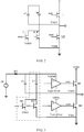
- FIG. 3 is a schematic structural diagram of still another power supply circuit according to an embodiment of this application.
- FIG. 3 also shows only one channel of the multi-phase modulation power supply circuit, and shows only some elements on the channel.
- a power supply chip includes a power supply DC, a diode D1, a second capacitor C1, a first driver, a second driver, a third switching transistor M1, and a fourth switching transistor M2.
- the power supply circuit in this embodiment of the present invention is improved on a basis of the power supply chip, where a first capacitor C1', a first switching transistor M1', and a second switching transistor M2' are added.
- a second electrode of the first switching transistor M1' and a second electrode of the third switching transistor M1 each may be a gate of a MOS transistor or a base of a transistor.
- a first electrode may be a source of the MOS transistor or a collector of the transistor
- a third electrode may be a drain of the MOS transistor or an emitter of the transistor.
- Drive signals that are input at the second electrode of the first switching transistor M1' and the second electrode of the third switching transistor M1 are the same.
- a second electrode of the second switching transistor M2' and a second electrode of the fourth switching transistor M2 each may be a gate of a MOS transistor or a base of a transistor.
- a first electrode may be a source of the MOS transistor or a collector of the transistor
- a third electrode may be a drain of the MOS transistor or an emitter of the transistor.
- Drive signals that are input at the second electrode of the second switching transistor M2' and the second electrode of the fourth switching transistor M2 are the same.
- a working principle of the power supply circuit is as follows: When the third switching transistor M1 is turned off and the fourth switching transistor M2 is turned on, a lower plate of the second capacitor C1 is connected to a voltage source source of lowside VSSL.
- the drive signals that are input at the second electrode of the first switching transistor M1' and the second electrode of the third switching transistor M1 are the same, and the drive signals that are input at the second electrode of the second switching transistor M2' and the second electrode of the fourth switching transistor M2. Therefore, the first switching transistor M1' is turned off, the second switching transistor M2' is turned on, and a lower plate of the first capacitor C1' is connected to the voltage source source of lowside VSSL.
- both the first capacitor C1' and the second capacitor C1 are connected to the voltage source source of lowside VSSL.
- a lower plate of the second capacitor C1 is connected to an output node VSSH, and a potential of the lower plate of the second capacitor C1 is equal to a potential of a voltage drain drain (Voltage Drain Drain, VDD).
- VDD Voltage Drain Drain
- the first switching transistor M1' is turned on, the second switching transistor M2' is turned off, a lower plate of the first capacitor C1' is connected to the output node VSSH, a potential of the lower plate is also equal to the potential of the VDD, and the potentials of the lower plates of the first capacitor C1' and the second capacitor C1 are equal.
- an ideal charge storage capacity of the first capacitor C1' may be used to balance the charging charges of the second capacitor C1.
- a capacitance of the first capacitor C1' is N times a capacitance of the second capacitor C1, and N is greater than 1.
- the first capacitor C1' is larger, a charge storage capacity is larger, and fluctuation of a voltage difference between two terminals of the second capacitor C1 imposes less impact on the circuit. Therefore, a second capacitor with a capacitance as large as possible can be selected.
- the second capacitor may be selected based on an actual signal frequency. If a signal frequency is small, a second capacitor with a relatively large capacitance may be selected. If a signal frequency is large, a second capacitor with a relatively small capacitance may be selected.
- a type of the first switching transistor M1' is the same as a type of the third switching transistor M1, to ensure that the first switching transistor M1' and the third switching transistor M1 are both turned off or turned on when a same drive signal is input.
- a type of the second switching transistor M2' is the same as a type of the fourth switching transistor M2, to ensure that the second switching transistor M2' and the fourth switching transistor M2 are both turned off or turned on when a same drive signal is input.
- a size of the first switching transistor M1' is X times a size of the third switching transistor M1, a size of the second switching transistor M2' is Y times a size of the fourth switching transistor M2, and both X and Y are greater than 1. Because a larger size of a switching transistor indicates smaller impedance and a better heat dissipation effect, a first switching transistor M1' and a second switching transistor M2' of sizes as large as possible can be selected. In addition, the first switching transistor M1' and the second switching transistor M2' may be selected based on an actual signal frequency. Because a smaller signal frequency indicates larger impedance, a first switching transistor M1' of a relatively large size and a second switching transistor M2' of a relatively large size can be selected. Because a larger signal frequency indicates smaller impedance, a first switching transistor M1' of a relatively small size and a second switching transistor M2' of a relatively small size can be selected.
- the first capacitor C1' may be disposed inside the power supply chip, thereby facilitating integration of the power supply chip and reducing power consumption of the circuit.
- the first capacitor C1' may be disposed outside the power supply chip, thereby facilitating selection of a capacitor with a larger capacitance, and achieving a better effect of improving stability of the circuit.
- the first capacitor C1' may be disposed adjacent to the second capacitor.
- the first switching transistor M1' and the second switching transistor M2' may be disposed outside the power supply chip, or may be disposed inside the power supply chip.
- the first switching transistor M1', the second switching transistor M2', the third switching transistor M1, or the fourth switching transistor M2 includes but is not limited to a bipolar transistor (such as BJT), a metal-oxide semiconductor field-effect transistor (such as MOSFET), or various III-V compound semiconductors (such as SiGe, GaAs, InP, and GaN).
- the first capacitor C1' or the second capacitor C1 may include but is not limited to a ceramic capacitor, a tantalum capacitor, or an electrolytic capacitor.
- the charging charges of the second capacitor are balanced by using the ideal charge storage capacity of the first capacitor, so that stability of the voltage difference between the two terminals of the bootstrap capacitor is improved, and a problem that the voltage difference between the two terminals of the bootstrap capacitor is unstable is fundamentally resolved, instead of only alleviate an impact caused by mutual feed-through between all channels.
- This improves dynamic performance of a circuit system.
- only two switching transistors and one capacitor need to be added on a basis of the power supply chip, a small quantity of elements are added, and a layout location of the added element may be selected to be inside the power supply chip or outside the power supply chip according to an actual situation. Because a direct current cannot flow through the added element, the added element does not form a direct current path, and no additional static power consumption is added.
- the apparatus may be a wireless communications system.
- the power supply circuit may be a multi-phase modulation power supply system module, for example, an envelope tracking power supply providing a multi-phase modulation structure for a power amplifier module of the wireless communications system.
Landscapes
- Engineering & Computer Science (AREA)
- Power Engineering (AREA)
- Microelectronics & Electronic Packaging (AREA)
- Physics & Mathematics (AREA)
- Electromagnetism (AREA)
- General Physics & Mathematics (AREA)
- Radar, Positioning & Navigation (AREA)
- Automation & Control Theory (AREA)
- Amplifiers (AREA)
- Dc-Dc Converters (AREA)
Applications Claiming Priority (1)
| Application Number | Priority Date | Filing Date | Title |
|---|---|---|---|
| PCT/CN2018/084918 WO2019205104A1 (zh) | 2018-04-27 | 2018-04-27 | 一种电源电路及装置 |
Publications (3)
| Publication Number | Publication Date |
|---|---|
| EP3780368A1 true EP3780368A1 (de) | 2021-02-17 |
| EP3780368A4 EP3780368A4 (de) | 2021-03-24 |
| EP3780368B1 EP3780368B1 (de) | 2023-12-13 |
Family
ID=68294317
Family Applications (1)
| Application Number | Title | Priority Date | Filing Date |
|---|---|---|---|
| EP18916536.8A Active EP3780368B1 (de) | 2018-04-27 | 2018-04-27 | Stromversorgungsschaltung und -vorrichtung |
Country Status (4)
| Country | Link |
|---|---|
| US (1) | US11201620B2 (de) |
| EP (1) | EP3780368B1 (de) |
| CN (2) | CN114362538A (de) |
| WO (1) | WO2019205104A1 (de) |
Cited By (1)
| Publication number | Priority date | Publication date | Assignee | Title |
|---|---|---|---|---|
| TWI832411B (zh) * | 2022-09-02 | 2024-02-11 | 康舒科技股份有限公司 | 自舉電容穩壓輔助電路及具有自舉電容穩壓輔助電路的電源轉換器 |
Family Cites Families (12)
| Publication number | Priority date | Publication date | Assignee | Title |
|---|---|---|---|---|
| US6256215B1 (en) * | 2000-08-10 | 2001-07-03 | Delphi Technologies, Inc. | Multiple output bootstrapped gate drive circuit |
| CN100592153C (zh) * | 2007-06-08 | 2010-02-24 | 群康科技(深圳)有限公司 | 负电压产生电路 |
| JP5309683B2 (ja) * | 2008-05-13 | 2013-10-09 | 株式会社リコー | 降圧型スイッチングレギュレータ |
| US8174248B2 (en) * | 2009-05-16 | 2012-05-08 | Texas Instruments Incorporated | Systems and methods of bit stuffing pulse width modulation |
| JP5330962B2 (ja) * | 2009-11-04 | 2013-10-30 | パナソニック株式会社 | Dc−dcコンバータ |
| CN101872208A (zh) * | 2010-06-23 | 2010-10-27 | 中兴通讯股份有限公司 | 一种电源调制器及电源调制方法 |
| US8680895B2 (en) * | 2010-10-08 | 2014-03-25 | Texas Instruments Incorporated | Controlling power chain with same controller in either of two different applications |
| US9419509B2 (en) * | 2014-08-11 | 2016-08-16 | Texas Instruments Incorporated | Shared bootstrap capacitor for multiple phase buck converter circuit and methods |
| US9595954B2 (en) * | 2014-11-10 | 2017-03-14 | Nxp Usa, Inc. | Method and circuit for recharging a bootstrap capacitor using a transfer capacitor |
| CN104539147B (zh) * | 2015-01-21 | 2017-05-31 | 青岛歌尔声学科技有限公司 | 一种电源电路及电子产品 |
| WO2017141559A1 (ja) * | 2016-02-16 | 2017-08-24 | 富士電機株式会社 | 半導体装置 |
| CN106059290B (zh) * | 2016-08-02 | 2019-01-15 | 成都芯源系统有限公司 | 多通道直流-直流变换器及控制电路和方法 |
-
2018
- 2018-04-27 WO PCT/CN2018/084918 patent/WO2019205104A1/zh not_active Ceased
- 2018-04-27 CN CN202111581522.1A patent/CN114362538A/zh active Pending
- 2018-04-27 CN CN201880092570.4A patent/CN111989851B/zh active Active
- 2018-04-27 EP EP18916536.8A patent/EP3780368B1/de active Active
-
2020
- 2020-10-26 US US17/079,857 patent/US11201620B2/en active Active
Cited By (1)
| Publication number | Priority date | Publication date | Assignee | Title |
|---|---|---|---|---|
| TWI832411B (zh) * | 2022-09-02 | 2024-02-11 | 康舒科技股份有限公司 | 自舉電容穩壓輔助電路及具有自舉電容穩壓輔助電路的電源轉換器 |
Also Published As
| Publication number | Publication date |
|---|---|
| CN111989851A (zh) | 2020-11-24 |
| EP3780368A4 (de) | 2021-03-24 |
| EP3780368B1 (de) | 2023-12-13 |
| US20210044295A1 (en) | 2021-02-11 |
| US11201620B2 (en) | 2021-12-14 |
| WO2019205104A1 (zh) | 2019-10-31 |
| CN114362538A (zh) | 2022-04-15 |
| CN111989851B (zh) | 2022-01-14 |
Similar Documents
| Publication | Publication Date | Title |
|---|---|---|
| US12574029B2 (en) | Generating high dynamic voltage boost | |
| US9673766B1 (en) | Class F amplifiers using resonant circuits in an output matching network | |
| TW202318766A (zh) | 共振電路及操作一共振電路之方法 | |
| US20120268091A1 (en) | Switching circuit device and power supply device having same | |
| CN102668381A (zh) | 栅极下拉的mosfet | |
| JP2015506102A (ja) | 半導体モジュール及びその製造方法 | |
| Kinzer et al. | Monolithic HV GaN power ICs: performance and application | |
| US9401644B2 (en) | Trench MOSFET having an independent coupled element in a trench | |
| US10200030B2 (en) | Paralleling of switching devices for high power circuits | |
| JP2018520625A (ja) | 電力コンバータの物理的トポロジー | |
| Zhang et al. | High-frequency integrated gate drivers for half-bridge GaN power stage | |
| WO2019159655A1 (ja) | 整流回路および電源装置 | |
| TWI810702B (zh) | 功率模組 | |
| Peng et al. | A 100 MHz two-phase four-segment DC-DC converter with light load efficiency enhancement in 0.18/spl mu/m CMOS | |
| CN113054969B (zh) | 一种氮化镓三极管栅极驱动电路及其控制方法 | |
| US11201620B2 (en) | Power supply circuit and apparatus | |
| CN108322043A (zh) | 一种单级有源阻抗网络dc-dc变换器 | |
| Hühn et al. | High efficiency, high bandwidth switch-mode envelope tracking supply modulator | |
| Hirose et al. | GaN HEMT technology for environmentally friendly power electronics | |
| Tian et al. | Monolithic Integration of p-GaN HEMT With Antiparallel Lateral Rectifier to Reduce the Negative Resistance Effect | |
| CN118748491B (zh) | 基于多回路复频域分析的中压SiC模块吸收电路设计方法 | |
| CN107094009B (zh) | 一种碳化硅场效应管的驱动模块 | |
| JP2016082335A (ja) | 半導体装置 | |
| CN117559776A (zh) | 功率转换电路及其控制方法 | |
| CN116614121A (zh) | 一种改善电磁兼容的功率器件 |
Legal Events
| Date | Code | Title | Description |
|---|---|---|---|
| STAA | Information on the status of an ep patent application or granted ep patent |
Free format text: STATUS: THE INTERNATIONAL PUBLICATION HAS BEEN MADE |
|
| PUAI | Public reference made under article 153(3) epc to a published international application that has entered the european phase |
Free format text: ORIGINAL CODE: 0009012 |
|
| STAA | Information on the status of an ep patent application or granted ep patent |
Free format text: STATUS: REQUEST FOR EXAMINATION WAS MADE |
|
| 17P | Request for examination filed |
Effective date: 20201104 |
|
| AK | Designated contracting states |
Kind code of ref document: A1 Designated state(s): AL AT BE BG CH CY CZ DE DK EE ES FI FR GB GR HR HU IE IS IT LI LT LU LV MC MK MT NL NO PL PT RO RS SE SI SK SM TR |
|
| AX | Request for extension of the european patent |
Extension state: BA ME |
|
| A4 | Supplementary search report drawn up and despatched |
Effective date: 20210223 |
|
| RIC1 | Information provided on ipc code assigned before grant |
Ipc: H03K 17/0412 20060101ALI20210217BHEP Ipc: G05F 1/46 20060101ALI20210217BHEP Ipc: H02M 3/155 20060101AFI20210217BHEP Ipc: H02M 3/156 20060101ALI20210217BHEP Ipc: H02M 3/335 20060101ALI20210217BHEP |
|
| DAV | Request for validation of the european patent (deleted) | ||
| DAX | Request for extension of the european patent (deleted) | ||
| RIC1 | Information provided on ipc code assigned before grant |
Ipc: H03K 17/0412 20060101ALI20230713BHEP Ipc: G05F 1/46 20060101ALI20230713BHEP Ipc: H02M 3/156 20060101ALI20230713BHEP Ipc: H02M 3/335 20060101ALI20230713BHEP Ipc: H02M 3/155 20060101AFI20230713BHEP |
|
| GRAP | Despatch of communication of intention to grant a patent |
Free format text: ORIGINAL CODE: EPIDOSNIGR1 |
|
| STAA | Information on the status of an ep patent application or granted ep patent |
Free format text: STATUS: GRANT OF PATENT IS INTENDED |
|
| INTG | Intention to grant announced |
Effective date: 20230829 |
|
| GRAS | Grant fee paid |
Free format text: ORIGINAL CODE: EPIDOSNIGR3 |
|
| GRAA | (expected) grant |
Free format text: ORIGINAL CODE: 0009210 |
|
| STAA | Information on the status of an ep patent application or granted ep patent |
Free format text: STATUS: THE PATENT HAS BEEN GRANTED |
|
| AK | Designated contracting states |
Kind code of ref document: B1 Designated state(s): AL AT BE BG CH CY CZ DE DK EE ES FI FR GB GR HR HU IE IS IT LI LT LU LV MC MK MT NL NO PL PT RO RS SE SI SK SM TR |
|
| REG | Reference to a national code |
Ref country code: GB Ref legal event code: FG4D |
|
| REG | Reference to a national code |
Ref country code: CH Ref legal event code: EP |
|
| P01 | Opt-out of the competence of the unified patent court (upc) registered |
Effective date: 20231121 |
|
| REG | Reference to a national code |
Ref country code: DE Ref legal event code: R096 Ref document number: 602018062775 Country of ref document: DE |
|
| REG | Reference to a national code |
Ref country code: IE Ref legal event code: FG4D |
|
| PG25 | Lapsed in a contracting state [announced via postgrant information from national office to epo] |
Ref country code: GR Free format text: LAPSE BECAUSE OF FAILURE TO SUBMIT A TRANSLATION OF THE DESCRIPTION OR TO PAY THE FEE WITHIN THE PRESCRIBED TIME-LIMIT Effective date: 20240314 |
|
| REG | Reference to a national code |
Ref country code: LT Ref legal event code: MG9D |
|
| PG25 | Lapsed in a contracting state [announced via postgrant information from national office to epo] |
Ref country code: LT Free format text: LAPSE BECAUSE OF FAILURE TO SUBMIT A TRANSLATION OF THE DESCRIPTION OR TO PAY THE FEE WITHIN THE PRESCRIBED TIME-LIMIT Effective date: 20231213 |
|
| REG | Reference to a national code |
Ref country code: NL Ref legal event code: MP Effective date: 20231213 |
|
| PG25 | Lapsed in a contracting state [announced via postgrant information from national office to epo] |
Ref country code: ES Free format text: LAPSE BECAUSE OF FAILURE TO SUBMIT A TRANSLATION OF THE DESCRIPTION OR TO PAY THE FEE WITHIN THE PRESCRIBED TIME-LIMIT Effective date: 20231213 |
|
| PG25 | Lapsed in a contracting state [announced via postgrant information from national office to epo] |
Ref country code: LT Free format text: LAPSE BECAUSE OF FAILURE TO SUBMIT A TRANSLATION OF THE DESCRIPTION OR TO PAY THE FEE WITHIN THE PRESCRIBED TIME-LIMIT Effective date: 20231213 Ref country code: GR Free format text: LAPSE BECAUSE OF FAILURE TO SUBMIT A TRANSLATION OF THE DESCRIPTION OR TO PAY THE FEE WITHIN THE PRESCRIBED TIME-LIMIT Effective date: 20240314 Ref country code: ES Free format text: LAPSE BECAUSE OF FAILURE TO SUBMIT A TRANSLATION OF THE DESCRIPTION OR TO PAY THE FEE WITHIN THE PRESCRIBED TIME-LIMIT Effective date: 20231213 Ref country code: BG Free format text: LAPSE BECAUSE OF FAILURE TO SUBMIT A TRANSLATION OF THE DESCRIPTION OR TO PAY THE FEE WITHIN THE PRESCRIBED TIME-LIMIT Effective date: 20240313 |
|
| REG | Reference to a national code |
Ref country code: AT Ref legal event code: MK05 Ref document number: 1641323 Country of ref document: AT Kind code of ref document: T Effective date: 20231213 |
|
| PG25 | Lapsed in a contracting state [announced via postgrant information from national office to epo] |
Ref country code: NL Free format text: LAPSE BECAUSE OF FAILURE TO SUBMIT A TRANSLATION OF THE DESCRIPTION OR TO PAY THE FEE WITHIN THE PRESCRIBED TIME-LIMIT Effective date: 20231213 |
|
| PG25 | Lapsed in a contracting state [announced via postgrant information from national office to epo] |
Ref country code: SE Free format text: LAPSE BECAUSE OF FAILURE TO SUBMIT A TRANSLATION OF THE DESCRIPTION OR TO PAY THE FEE WITHIN THE PRESCRIBED TIME-LIMIT Effective date: 20231213 Ref country code: RS Free format text: LAPSE BECAUSE OF FAILURE TO SUBMIT A TRANSLATION OF THE DESCRIPTION OR TO PAY THE FEE WITHIN THE PRESCRIBED TIME-LIMIT Effective date: 20231213 Ref country code: NO Free format text: LAPSE BECAUSE OF FAILURE TO SUBMIT A TRANSLATION OF THE DESCRIPTION OR TO PAY THE FEE WITHIN THE PRESCRIBED TIME-LIMIT Effective date: 20240313 Ref country code: NL Free format text: LAPSE BECAUSE OF FAILURE TO SUBMIT A TRANSLATION OF THE DESCRIPTION OR TO PAY THE FEE WITHIN THE PRESCRIBED TIME-LIMIT Effective date: 20231213 Ref country code: LV Free format text: LAPSE BECAUSE OF FAILURE TO SUBMIT A TRANSLATION OF THE DESCRIPTION OR TO PAY THE FEE WITHIN THE PRESCRIBED TIME-LIMIT Effective date: 20231213 Ref country code: HR Free format text: LAPSE BECAUSE OF FAILURE TO SUBMIT A TRANSLATION OF THE DESCRIPTION OR TO PAY THE FEE WITHIN THE PRESCRIBED TIME-LIMIT Effective date: 20231213 |
|
| PG25 | Lapsed in a contracting state [announced via postgrant information from national office to epo] |
Ref country code: IS Free format text: LAPSE BECAUSE OF FAILURE TO SUBMIT A TRANSLATION OF THE DESCRIPTION OR TO PAY THE FEE WITHIN THE PRESCRIBED TIME-LIMIT Effective date: 20240413 |
|
| PG25 | Lapsed in a contracting state [announced via postgrant information from national office to epo] |
Ref country code: AT Free format text: LAPSE BECAUSE OF FAILURE TO SUBMIT A TRANSLATION OF THE DESCRIPTION OR TO PAY THE FEE WITHIN THE PRESCRIBED TIME-LIMIT Effective date: 20231213 Ref country code: CZ Free format text: LAPSE BECAUSE OF FAILURE TO SUBMIT A TRANSLATION OF THE DESCRIPTION OR TO PAY THE FEE WITHIN THE PRESCRIBED TIME-LIMIT Effective date: 20231213 |
|
| PG25 | Lapsed in a contracting state [announced via postgrant information from national office to epo] |
Ref country code: SK Free format text: LAPSE BECAUSE OF FAILURE TO SUBMIT A TRANSLATION OF THE DESCRIPTION OR TO PAY THE FEE WITHIN THE PRESCRIBED TIME-LIMIT Effective date: 20231213 |
|
| PG25 | Lapsed in a contracting state [announced via postgrant information from national office to epo] |
Ref country code: SM Free format text: LAPSE BECAUSE OF FAILURE TO SUBMIT A TRANSLATION OF THE DESCRIPTION OR TO PAY THE FEE WITHIN THE PRESCRIBED TIME-LIMIT Effective date: 20231213 Ref country code: SK Free format text: LAPSE BECAUSE OF FAILURE TO SUBMIT A TRANSLATION OF THE DESCRIPTION OR TO PAY THE FEE WITHIN THE PRESCRIBED TIME-LIMIT Effective date: 20231213 Ref country code: RO Free format text: LAPSE BECAUSE OF FAILURE TO SUBMIT A TRANSLATION OF THE DESCRIPTION OR TO PAY THE FEE WITHIN THE PRESCRIBED TIME-LIMIT Effective date: 20231213 Ref country code: IT Free format text: LAPSE BECAUSE OF FAILURE TO SUBMIT A TRANSLATION OF THE DESCRIPTION OR TO PAY THE FEE WITHIN THE PRESCRIBED TIME-LIMIT Effective date: 20231213 Ref country code: IS Free format text: LAPSE BECAUSE OF FAILURE TO SUBMIT A TRANSLATION OF THE DESCRIPTION OR TO PAY THE FEE WITHIN THE PRESCRIBED TIME-LIMIT Effective date: 20240413 Ref country code: EE Free format text: LAPSE BECAUSE OF FAILURE TO SUBMIT A TRANSLATION OF THE DESCRIPTION OR TO PAY THE FEE WITHIN THE PRESCRIBED TIME-LIMIT Effective date: 20231213 Ref country code: CZ Free format text: LAPSE BECAUSE OF FAILURE TO SUBMIT A TRANSLATION OF THE DESCRIPTION OR TO PAY THE FEE WITHIN THE PRESCRIBED TIME-LIMIT Effective date: 20231213 Ref country code: AT Free format text: LAPSE BECAUSE OF FAILURE TO SUBMIT A TRANSLATION OF THE DESCRIPTION OR TO PAY THE FEE WITHIN THE PRESCRIBED TIME-LIMIT Effective date: 20231213 |
|
| PG25 | Lapsed in a contracting state [announced via postgrant information from national office to epo] |
Ref country code: PL Free format text: LAPSE BECAUSE OF FAILURE TO SUBMIT A TRANSLATION OF THE DESCRIPTION OR TO PAY THE FEE WITHIN THE PRESCRIBED TIME-LIMIT Effective date: 20231213 Ref country code: PT Free format text: LAPSE BECAUSE OF FAILURE TO SUBMIT A TRANSLATION OF THE DESCRIPTION OR TO PAY THE FEE WITHIN THE PRESCRIBED TIME-LIMIT Effective date: 20240415 |
|
| PG25 | Lapsed in a contracting state [announced via postgrant information from national office to epo] |
Ref country code: PT Free format text: LAPSE BECAUSE OF FAILURE TO SUBMIT A TRANSLATION OF THE DESCRIPTION OR TO PAY THE FEE WITHIN THE PRESCRIBED TIME-LIMIT Effective date: 20240415 Ref country code: PL Free format text: LAPSE BECAUSE OF FAILURE TO SUBMIT A TRANSLATION OF THE DESCRIPTION OR TO PAY THE FEE WITHIN THE PRESCRIBED TIME-LIMIT Effective date: 20231213 |
|
| REG | Reference to a national code |
Ref country code: DE Ref legal event code: R097 Ref document number: 602018062775 Country of ref document: DE |
|
| PG25 | Lapsed in a contracting state [announced via postgrant information from national office to epo] |
Ref country code: DK Free format text: LAPSE BECAUSE OF FAILURE TO SUBMIT A TRANSLATION OF THE DESCRIPTION OR TO PAY THE FEE WITHIN THE PRESCRIBED TIME-LIMIT Effective date: 20231213 |
|
| PLBE | No opposition filed within time limit |
Free format text: ORIGINAL CODE: 0009261 |
|
| STAA | Information on the status of an ep patent application or granted ep patent |
Free format text: STATUS: NO OPPOSITION FILED WITHIN TIME LIMIT |
|
| PG25 | Lapsed in a contracting state [announced via postgrant information from national office to epo] |
Ref country code: SI Free format text: LAPSE BECAUSE OF FAILURE TO SUBMIT A TRANSLATION OF THE DESCRIPTION OR TO PAY THE FEE WITHIN THE PRESCRIBED TIME-LIMIT Effective date: 20231213 |
|
| PG25 | Lapsed in a contracting state [announced via postgrant information from national office to epo] |
Ref country code: SI Free format text: LAPSE BECAUSE OF FAILURE TO SUBMIT A TRANSLATION OF THE DESCRIPTION OR TO PAY THE FEE WITHIN THE PRESCRIBED TIME-LIMIT Effective date: 20231213 Ref country code: DK Free format text: LAPSE BECAUSE OF FAILURE TO SUBMIT A TRANSLATION OF THE DESCRIPTION OR TO PAY THE FEE WITHIN THE PRESCRIBED TIME-LIMIT Effective date: 20231213 |
|
| 26N | No opposition filed |
Effective date: 20240916 |
|
| PG25 | Lapsed in a contracting state [announced via postgrant information from national office to epo] |
Ref country code: MC Free format text: LAPSE BECAUSE OF FAILURE TO SUBMIT A TRANSLATION OF THE DESCRIPTION OR TO PAY THE FEE WITHIN THE PRESCRIBED TIME-LIMIT Effective date: 20231213 |
|
| PG25 | Lapsed in a contracting state [announced via postgrant information from national office to epo] |
Ref country code: MC Free format text: LAPSE BECAUSE OF FAILURE TO SUBMIT A TRANSLATION OF THE DESCRIPTION OR TO PAY THE FEE WITHIN THE PRESCRIBED TIME-LIMIT Effective date: 20231213 |
|
| REG | Reference to a national code |
Ref country code: CH Ref legal event code: PL |
|
| PG25 | Lapsed in a contracting state [announced via postgrant information from national office to epo] |
Ref country code: LU Free format text: LAPSE BECAUSE OF NON-PAYMENT OF DUE FEES Effective date: 20240427 |
|
| REG | Reference to a national code |
Ref country code: BE Ref legal event code: MM Effective date: 20240430 |
|
| PG25 | Lapsed in a contracting state [announced via postgrant information from national office to epo] |
Ref country code: LU Free format text: LAPSE BECAUSE OF NON-PAYMENT OF DUE FEES Effective date: 20240427 |
|
| PG25 | Lapsed in a contracting state [announced via postgrant information from national office to epo] |
Ref country code: BE Free format text: LAPSE BECAUSE OF NON-PAYMENT OF DUE FEES Effective date: 20240430 |
|
| PG25 | Lapsed in a contracting state [announced via postgrant information from national office to epo] |
Ref country code: BE Free format text: LAPSE BECAUSE OF NON-PAYMENT OF DUE FEES Effective date: 20240430 Ref country code: CH Free format text: LAPSE BECAUSE OF NON-PAYMENT OF DUE FEES Effective date: 20240430 |
|
| PG25 | Lapsed in a contracting state [announced via postgrant information from national office to epo] |
Ref country code: IE Free format text: LAPSE BECAUSE OF NON-PAYMENT OF DUE FEES Effective date: 20240427 |
|
| PGFP | Annual fee paid to national office [announced via postgrant information from national office to epo] |
Ref country code: FR Payment date: 20250310 Year of fee payment: 8 |
|
| PGFP | Annual fee paid to national office [announced via postgrant information from national office to epo] |
Ref country code: GB Payment date: 20250306 Year of fee payment: 8 |
|
| PGFP | Annual fee paid to national office [announced via postgrant information from national office to epo] |
Ref country code: DE Payment date: 20250305 Year of fee payment: 8 |
|
| PG25 | Lapsed in a contracting state [announced via postgrant information from national office to epo] |
Ref country code: CY Free format text: LAPSE BECAUSE OF FAILURE TO SUBMIT A TRANSLATION OF THE DESCRIPTION OR TO PAY THE FEE WITHIN THE PRESCRIBED TIME-LIMIT; INVALID AB INITIO Effective date: 20180427 |
|
| PG25 | Lapsed in a contracting state [announced via postgrant information from national office to epo] |
Ref country code: HU Free format text: LAPSE BECAUSE OF FAILURE TO SUBMIT A TRANSLATION OF THE DESCRIPTION OR TO PAY THE FEE WITHIN THE PRESCRIBED TIME-LIMIT; INVALID AB INITIO Effective date: 20180427 |
|
| PG25 | Lapsed in a contracting state [announced via postgrant information from national office to epo] |
Ref country code: FI Free format text: LAPSE BECAUSE OF FAILURE TO SUBMIT A TRANSLATION OF THE DESCRIPTION OR TO PAY THE FEE WITHIN THE PRESCRIBED TIME-LIMIT Effective date: 20231213 |