EP3772666B1 - Abdeckfenster und flexible anzeigevorrichtung damit - Google Patents
Abdeckfenster und flexible anzeigevorrichtung damit Download PDFInfo
- Publication number
- EP3772666B1 EP3772666B1 EP20189332.8A EP20189332A EP3772666B1 EP 3772666 B1 EP3772666 B1 EP 3772666B1 EP 20189332 A EP20189332 A EP 20189332A EP 3772666 B1 EP3772666 B1 EP 3772666B1
- Authority
- EP
- European Patent Office
- Prior art keywords
- layer
- cover window
- display device
- inorganic
- polymer film
- Prior art date
- Legal status (The legal status is an assumption and is not a legal conclusion. Google has not performed a legal analysis and makes no representation as to the accuracy of the status listed.)
- Active
Links
Images


Classifications
-
- G—PHYSICS
- G02—OPTICS
- G02B—OPTICAL ELEMENTS, SYSTEMS OR APPARATUS
- G02B1/00—Optical elements characterised by the material of which they are made; Optical coatings for optical elements
- G02B1/10—Optical coatings produced by application to, or surface treatment of, optical elements
- G02B1/14—Protective coatings, e.g. hard coatings
-
- H—ELECTRICITY
- H10—SEMICONDUCTOR DEVICES; ELECTRIC SOLID-STATE DEVICES NOT OTHERWISE PROVIDED FOR
- H10K—ORGANIC ELECTRIC SOLID-STATE DEVICES
- H10K59/00—Integrated devices, or assemblies of multiple devices, comprising at least one organic light-emitting element covered by group H10K50/00
- H10K59/10—OLED displays
- H10K59/12—Active-matrix OLED [AMOLED] displays
-
- B—PERFORMING OPERATIONS; TRANSPORTING
- B32—LAYERED PRODUCTS
- B32B—LAYERED PRODUCTS, i.e. PRODUCTS BUILT-UP OF STRATA OF FLAT OR NON-FLAT, e.g. CELLULAR OR HONEYCOMB, FORM
- B32B15/00—Layered products comprising a layer of metal
- B32B15/04—Layered products comprising a layer of metal comprising metal as the main or only constituent of a layer, which is next to another layer of the same or of a different material
- B32B15/08—Layered products comprising a layer of metal comprising metal as the main or only constituent of a layer, which is next to another layer of the same or of a different material of synthetic resin
- B32B15/088—Layered products comprising a layer of metal comprising metal as the main or only constituent of a layer, which is next to another layer of the same or of a different material of synthetic resin comprising polyamides
-
- B—PERFORMING OPERATIONS; TRANSPORTING
- B32—LAYERED PRODUCTS
- B32B—LAYERED PRODUCTS, i.e. PRODUCTS BUILT-UP OF STRATA OF FLAT OR NON-FLAT, e.g. CELLULAR OR HONEYCOMB, FORM
- B32B15/00—Layered products comprising a layer of metal
- B32B15/04—Layered products comprising a layer of metal comprising metal as the main or only constituent of a layer, which is next to another layer of the same or of a different material
- B32B15/08—Layered products comprising a layer of metal comprising metal as the main or only constituent of a layer, which is next to another layer of the same or of a different material of synthetic resin
- B32B15/09—Layered products comprising a layer of metal comprising metal as the main or only constituent of a layer, which is next to another layer of the same or of a different material of synthetic resin comprising polyesters
-
- B—PERFORMING OPERATIONS; TRANSPORTING
- B32—LAYERED PRODUCTS
- B32B—LAYERED PRODUCTS, i.e. PRODUCTS BUILT-UP OF STRATA OF FLAT OR NON-FLAT, e.g. CELLULAR OR HONEYCOMB, FORM
- B32B15/00—Layered products comprising a layer of metal
- B32B15/18—Layered products comprising a layer of metal comprising iron or steel
-
- B—PERFORMING OPERATIONS; TRANSPORTING
- B32—LAYERED PRODUCTS
- B32B—LAYERED PRODUCTS, i.e. PRODUCTS BUILT-UP OF STRATA OF FLAT OR NON-FLAT, e.g. CELLULAR OR HONEYCOMB, FORM
- B32B27/00—Layered products comprising a layer of synthetic resin
- B32B27/06—Layered products comprising a layer of synthetic resin as the main or only constituent of a layer, which is next to another layer of the same or of a different material
- B32B27/08—Layered products comprising a layer of synthetic resin as the main or only constituent of a layer, which is next to another layer of the same or of a different material of synthetic resin
-
- B—PERFORMING OPERATIONS; TRANSPORTING
- B32—LAYERED PRODUCTS
- B32B—LAYERED PRODUCTS, i.e. PRODUCTS BUILT-UP OF STRATA OF FLAT OR NON-FLAT, e.g. CELLULAR OR HONEYCOMB, FORM
- B32B27/00—Layered products comprising a layer of synthetic resin
- B32B27/28—Layered products comprising a layer of synthetic resin comprising synthetic resins not wholly covered by any one of the sub-groups B32B27/30 - B32B27/42
- B32B27/281—Layered products comprising a layer of synthetic resin comprising synthetic resins not wholly covered by any one of the sub-groups B32B27/30 - B32B27/42 comprising polyimides
-
- B—PERFORMING OPERATIONS; TRANSPORTING
- B32—LAYERED PRODUCTS
- B32B—LAYERED PRODUCTS, i.e. PRODUCTS BUILT-UP OF STRATA OF FLAT OR NON-FLAT, e.g. CELLULAR OR HONEYCOMB, FORM
- B32B27/00—Layered products comprising a layer of synthetic resin
- B32B27/28—Layered products comprising a layer of synthetic resin comprising synthetic resins not wholly covered by any one of the sub-groups B32B27/30 - B32B27/42
- B32B27/283—Layered products comprising a layer of synthetic resin comprising synthetic resins not wholly covered by any one of the sub-groups B32B27/30 - B32B27/42 comprising polysiloxanes
-
- B—PERFORMING OPERATIONS; TRANSPORTING
- B32—LAYERED PRODUCTS
- B32B—LAYERED PRODUCTS, i.e. PRODUCTS BUILT-UP OF STRATA OF FLAT OR NON-FLAT, e.g. CELLULAR OR HONEYCOMB, FORM
- B32B27/00—Layered products comprising a layer of synthetic resin
- B32B27/30—Layered products comprising a layer of synthetic resin comprising vinyl (co)polymers; comprising acrylic (co)polymers
- B32B27/302—Layered products comprising a layer of synthetic resin comprising vinyl (co)polymers; comprising acrylic (co)polymers comprising aromatic vinyl (co)polymers, e.g. styrenic (co)polymers
-
- B—PERFORMING OPERATIONS; TRANSPORTING
- B32—LAYERED PRODUCTS
- B32B—LAYERED PRODUCTS, i.e. PRODUCTS BUILT-UP OF STRATA OF FLAT OR NON-FLAT, e.g. CELLULAR OR HONEYCOMB, FORM
- B32B27/00—Layered products comprising a layer of synthetic resin
- B32B27/30—Layered products comprising a layer of synthetic resin comprising vinyl (co)polymers; comprising acrylic (co)polymers
- B32B27/308—Layered products comprising a layer of synthetic resin comprising vinyl (co)polymers; comprising acrylic (co)polymers comprising acrylic (co)polymers
-
- B—PERFORMING OPERATIONS; TRANSPORTING
- B32—LAYERED PRODUCTS
- B32B—LAYERED PRODUCTS, i.e. PRODUCTS BUILT-UP OF STRATA OF FLAT OR NON-FLAT, e.g. CELLULAR OR HONEYCOMB, FORM
- B32B27/00—Layered products comprising a layer of synthetic resin
- B32B27/34—Layered products comprising a layer of synthetic resin comprising polyamides
-
- B—PERFORMING OPERATIONS; TRANSPORTING
- B32—LAYERED PRODUCTS
- B32B—LAYERED PRODUCTS, i.e. PRODUCTS BUILT-UP OF STRATA OF FLAT OR NON-FLAT, e.g. CELLULAR OR HONEYCOMB, FORM
- B32B27/00—Layered products comprising a layer of synthetic resin
- B32B27/36—Layered products comprising a layer of synthetic resin comprising polyesters
- B32B27/365—Layered products comprising a layer of synthetic resin comprising polyesters comprising polycarbonates
-
- B—PERFORMING OPERATIONS; TRANSPORTING
- B32—LAYERED PRODUCTS
- B32B—LAYERED PRODUCTS, i.e. PRODUCTS BUILT-UP OF STRATA OF FLAT OR NON-FLAT, e.g. CELLULAR OR HONEYCOMB, FORM
- B32B27/00—Layered products comprising a layer of synthetic resin
- B32B27/40—Layered products comprising a layer of synthetic resin comprising polyurethanes
-
- B—PERFORMING OPERATIONS; TRANSPORTING
- B32—LAYERED PRODUCTS
- B32B—LAYERED PRODUCTS, i.e. PRODUCTS BUILT-UP OF STRATA OF FLAT OR NON-FLAT, e.g. CELLULAR OR HONEYCOMB, FORM
- B32B7/00—Layered products characterised by the relation between layers; Layered products characterised by the relative orientation of features between layers, or by the relative values of a measurable parameter between layers, i.e. products comprising layers having different physical, chemical or physicochemical properties; Layered products characterised by the interconnection of layers
- B32B7/04—Interconnection of layers
- B32B7/12—Interconnection of layers using interposed adhesives or interposed materials with bonding properties
-
- C—CHEMISTRY; METALLURGY
- C09—DYES; PAINTS; POLISHES; NATURAL RESINS; ADHESIVES; COMPOSITIONS NOT OTHERWISE PROVIDED FOR; APPLICATIONS OF MATERIALS NOT OTHERWISE PROVIDED FOR
- C09D—COATING COMPOSITIONS, e.g. PAINTS, VARNISHES OR LACQUERS; FILLING PASTES; CHEMICAL PAINT OR INK REMOVERS; INKS; CORRECTING FLUIDS; WOODSTAINS; PASTES OR SOLIDS FOR COLOURING OR PRINTING; USE OF MATERIALS THEREFOR
- C09D1/00—Coating compositions, e.g. paints, varnishes or lacquers, based on inorganic substances
- C09D1/02—Coating compositions, e.g. paints, varnishes or lacquers, based on inorganic substances alkali metal silicates
-
- G—PHYSICS
- G02—OPTICS
- G02F—OPTICAL DEVICES OR ARRANGEMENTS FOR THE CONTROL OF LIGHT BY MODIFICATION OF THE OPTICAL PROPERTIES OF THE MEDIA OF THE ELEMENTS INVOLVED THEREIN; NON-LINEAR OPTICS; FREQUENCY-CHANGING OF LIGHT; OPTICAL LOGIC ELEMENTS; OPTICAL ANALOGUE/DIGITAL CONVERTERS
- G02F1/00—Devices or arrangements for the control of the intensity, colour, phase, polarisation or direction of light arriving from an independent light source, e.g. switching, gating or modulating; Non-linear optics
- G02F1/01—Devices or arrangements for the control of the intensity, colour, phase, polarisation or direction of light arriving from an independent light source, e.g. switching, gating or modulating; Non-linear optics for the control of the intensity, phase, polarisation or colour
- G02F1/13—Devices or arrangements for the control of the intensity, colour, phase, polarisation or direction of light arriving from an independent light source, e.g. switching, gating or modulating; Non-linear optics for the control of the intensity, phase, polarisation or colour based on liquid crystals, e.g. single liquid crystal display cells
- G02F1/133—Constructional arrangements; Operation of liquid crystal cells; Circuit arrangements
- G02F1/1333—Constructional arrangements; Manufacturing methods
- G02F1/133305—Flexible substrates, e.g. plastics, organic film
-
- G—PHYSICS
- G02—OPTICS
- G02F—OPTICAL DEVICES OR ARRANGEMENTS FOR THE CONTROL OF LIGHT BY MODIFICATION OF THE OPTICAL PROPERTIES OF THE MEDIA OF THE ELEMENTS INVOLVED THEREIN; NON-LINEAR OPTICS; FREQUENCY-CHANGING OF LIGHT; OPTICAL LOGIC ELEMENTS; OPTICAL ANALOGUE/DIGITAL CONVERTERS
- G02F1/00—Devices or arrangements for the control of the intensity, colour, phase, polarisation or direction of light arriving from an independent light source, e.g. switching, gating or modulating; Non-linear optics
- G02F1/01—Devices or arrangements for the control of the intensity, colour, phase, polarisation or direction of light arriving from an independent light source, e.g. switching, gating or modulating; Non-linear optics for the control of the intensity, phase, polarisation or colour
- G02F1/13—Devices or arrangements for the control of the intensity, colour, phase, polarisation or direction of light arriving from an independent light source, e.g. switching, gating or modulating; Non-linear optics for the control of the intensity, phase, polarisation or colour based on liquid crystals, e.g. single liquid crystal display cells
- G02F1/133—Constructional arrangements; Operation of liquid crystal cells; Circuit arrangements
- G02F1/1333—Constructional arrangements; Manufacturing methods
- G02F1/133308—Support structures for LCD panels, e.g. frames or bezels
- G02F1/133331—Cover glasses
-
- G—PHYSICS
- G06—COMPUTING OR CALCULATING; COUNTING
- G06F—ELECTRIC DIGITAL DATA PROCESSING
- G06F1/00—Details not covered by groups G06F3/00 - G06F13/00 and G06F21/00
- G06F1/16—Constructional details or arrangements
- G06F1/1601—Constructional details related to the housing of computer displays, e.g. of CRT monitors, of flat displays
- G06F1/1607—Arrangements to support accessories mechanically attached to the display housing
- G06F1/1609—Arrangements to support accessories mechanically attached to the display housing to support filters or lenses
-
- G—PHYSICS
- G06—COMPUTING OR CALCULATING; COUNTING
- G06F—ELECTRIC DIGITAL DATA PROCESSING
- G06F1/00—Details not covered by groups G06F3/00 - G06F13/00 and G06F21/00
- G06F1/16—Constructional details or arrangements
- G06F1/1613—Constructional details or arrangements for portable computers
- G06F1/1633—Constructional details or arrangements of portable computers not specific to the type of enclosures covered by groups G06F1/1615 - G06F1/1626
- G06F1/1637—Details related to the display arrangement, including those related to the mounting of the display in the housing
- G06F1/1641—Details related to the display arrangement, including those related to the mounting of the display in the housing the display being formed by a plurality of foldable display components
-
- G—PHYSICS
- G06—COMPUTING OR CALCULATING; COUNTING
- G06F—ELECTRIC DIGITAL DATA PROCESSING
- G06F1/00—Details not covered by groups G06F3/00 - G06F13/00 and G06F21/00
- G06F1/16—Constructional details or arrangements
- G06F1/1613—Constructional details or arrangements for portable computers
- G06F1/1633—Constructional details or arrangements of portable computers not specific to the type of enclosures covered by groups G06F1/1615 - G06F1/1626
- G06F1/1637—Details related to the display arrangement, including those related to the mounting of the display in the housing
- G06F1/1652—Details related to the display arrangement, including those related to the mounting of the display in the housing the display being flexible, e.g. mimicking a sheet of paper, or rollable
-
- G—PHYSICS
- G09—EDUCATION; CRYPTOGRAPHY; DISPLAY; ADVERTISING; SEALS
- G09F—DISPLAYING; ADVERTISING; SIGNS; LABELS OR NAME-PLATES; SEALS
- G09F9/00—Indicating arrangements for variable information in which the information is built-up on a support by selection or combination of individual elements
- G09F9/30—Indicating arrangements for variable information in which the information is built-up on a support by selection or combination of individual elements in which the desired character or characters are formed by combining individual elements
- G09F9/301—Indicating arrangements for variable information in which the information is built-up on a support by selection or combination of individual elements in which the desired character or characters are formed by combining individual elements flexible foldable or roll-able electronic displays, e.g. thin LCD, OLED
-
- H—ELECTRICITY
- H04—ELECTRIC COMMUNICATION TECHNIQUE
- H04M—TELEPHONIC COMMUNICATION
- H04M1/00—Substation equipment, e.g. for use by subscribers
- H04M1/02—Constructional features of telephone sets
- H04M1/0202—Portable telephone sets, e.g. cordless phones, mobile phones or bar type handsets
- H04M1/026—Details of the structure or mounting of specific components
- H04M1/0266—Details of the structure or mounting of specific components for a display module assembly
- H04M1/0268—Details of the structure or mounting of specific components for a display module assembly including a flexible display panel
-
- H—ELECTRICITY
- H10—SEMICONDUCTOR DEVICES; ELECTRIC SOLID-STATE DEVICES NOT OTHERWISE PROVIDED FOR
- H10K—ORGANIC ELECTRIC SOLID-STATE DEVICES
- H10K50/00—Organic light-emitting devices
- H10K50/80—Constructional details
- H10K50/84—Passivation; Containers; Encapsulations
- H10K50/841—Self-supporting sealing arrangements
-
- H—ELECTRICITY
- H10—SEMICONDUCTOR DEVICES; ELECTRIC SOLID-STATE DEVICES NOT OTHERWISE PROVIDED FOR
- H10K—ORGANIC ELECTRIC SOLID-STATE DEVICES
- H10K50/00—Organic light-emitting devices
- H10K50/80—Constructional details
- H10K50/84—Passivation; Containers; Encapsulations
- H10K50/844—Encapsulations
-
- B—PERFORMING OPERATIONS; TRANSPORTING
- B32—LAYERED PRODUCTS
- B32B—LAYERED PRODUCTS, i.e. PRODUCTS BUILT-UP OF STRATA OF FLAT OR NON-FLAT, e.g. CELLULAR OR HONEYCOMB, FORM
- B32B2255/00—Coating on the layer surface
- B32B2255/10—Coating on the layer surface on synthetic resin layer or on natural or synthetic rubber layer
-
- B—PERFORMING OPERATIONS; TRANSPORTING
- B32—LAYERED PRODUCTS
- B32B—LAYERED PRODUCTS, i.e. PRODUCTS BUILT-UP OF STRATA OF FLAT OR NON-FLAT, e.g. CELLULAR OR HONEYCOMB, FORM
- B32B2255/00—Coating on the layer surface
- B32B2255/20—Inorganic coating
-
- B—PERFORMING OPERATIONS; TRANSPORTING
- B32—LAYERED PRODUCTS
- B32B—LAYERED PRODUCTS, i.e. PRODUCTS BUILT-UP OF STRATA OF FLAT OR NON-FLAT, e.g. CELLULAR OR HONEYCOMB, FORM
- B32B2255/00—Coating on the layer surface
- B32B2255/26—Polymeric coating
-
- B—PERFORMING OPERATIONS; TRANSPORTING
- B32—LAYERED PRODUCTS
- B32B—LAYERED PRODUCTS, i.e. PRODUCTS BUILT-UP OF STRATA OF FLAT OR NON-FLAT, e.g. CELLULAR OR HONEYCOMB, FORM
- B32B2255/00—Coating on the layer surface
- B32B2255/28—Multiple coating on one surface
-
- B—PERFORMING OPERATIONS; TRANSPORTING
- B32—LAYERED PRODUCTS
- B32B—LAYERED PRODUCTS, i.e. PRODUCTS BUILT-UP OF STRATA OF FLAT OR NON-FLAT, e.g. CELLULAR OR HONEYCOMB, FORM
- B32B2307/00—Properties of the layers or laminate
- B32B2307/20—Properties of the layers or laminate having particular electrical or magnetic properties, e.g. piezoelectric
- B32B2307/202—Conductive
-
- B—PERFORMING OPERATIONS; TRANSPORTING
- B32—LAYERED PRODUCTS
- B32B—LAYERED PRODUCTS, i.e. PRODUCTS BUILT-UP OF STRATA OF FLAT OR NON-FLAT, e.g. CELLULAR OR HONEYCOMB, FORM
- B32B2307/00—Properties of the layers or laminate
- B32B2307/40—Properties of the layers or laminate having particular optical properties
- B32B2307/412—Transparent
-
- B—PERFORMING OPERATIONS; TRANSPORTING
- B32—LAYERED PRODUCTS
- B32B—LAYERED PRODUCTS, i.e. PRODUCTS BUILT-UP OF STRATA OF FLAT OR NON-FLAT, e.g. CELLULAR OR HONEYCOMB, FORM
- B32B2307/00—Properties of the layers or laminate
- B32B2307/50—Properties of the layers or laminate having particular mechanical properties
- B32B2307/51—Elastic
-
- B—PERFORMING OPERATIONS; TRANSPORTING
- B32—LAYERED PRODUCTS
- B32B—LAYERED PRODUCTS, i.e. PRODUCTS BUILT-UP OF STRATA OF FLAT OR NON-FLAT, e.g. CELLULAR OR HONEYCOMB, FORM
- B32B2307/00—Properties of the layers or laminate
- B32B2307/50—Properties of the layers or laminate having particular mechanical properties
- B32B2307/536—Hardness
-
- B—PERFORMING OPERATIONS; TRANSPORTING
- B32—LAYERED PRODUCTS
- B32B—LAYERED PRODUCTS, i.e. PRODUCTS BUILT-UP OF STRATA OF FLAT OR NON-FLAT, e.g. CELLULAR OR HONEYCOMB, FORM
- B32B2307/00—Properties of the layers or laminate
- B32B2307/50—Properties of the layers or laminate having particular mechanical properties
- B32B2307/54—Yield strength; Tensile strength
-
- B—PERFORMING OPERATIONS; TRANSPORTING
- B32—LAYERED PRODUCTS
- B32B—LAYERED PRODUCTS, i.e. PRODUCTS BUILT-UP OF STRATA OF FLAT OR NON-FLAT, e.g. CELLULAR OR HONEYCOMB, FORM
- B32B2307/00—Properties of the layers or laminate
- B32B2307/50—Properties of the layers or laminate having particular mechanical properties
- B32B2307/546—Flexural strength; Flexion stiffness
-
- B—PERFORMING OPERATIONS; TRANSPORTING
- B32—LAYERED PRODUCTS
- B32B—LAYERED PRODUCTS, i.e. PRODUCTS BUILT-UP OF STRATA OF FLAT OR NON-FLAT, e.g. CELLULAR OR HONEYCOMB, FORM
- B32B2307/00—Properties of the layers or laminate
- B32B2307/70—Other properties
- B32B2307/724—Permeability to gases, adsorption
- B32B2307/7242—Non-permeable
- B32B2307/7246—Water vapor barrier
-
- B—PERFORMING OPERATIONS; TRANSPORTING
- B32—LAYERED PRODUCTS
- B32B—LAYERED PRODUCTS, i.e. PRODUCTS BUILT-UP OF STRATA OF FLAT OR NON-FLAT, e.g. CELLULAR OR HONEYCOMB, FORM
- B32B2307/00—Properties of the layers or laminate
- B32B2307/70—Other properties
- B32B2307/732—Dimensional properties
-
- B—PERFORMING OPERATIONS; TRANSPORTING
- B32—LAYERED PRODUCTS
- B32B—LAYERED PRODUCTS, i.e. PRODUCTS BUILT-UP OF STRATA OF FLAT OR NON-FLAT, e.g. CELLULAR OR HONEYCOMB, FORM
- B32B2457/00—Electrical equipment
- B32B2457/20—Displays, e.g. liquid crystal displays, plasma displays
- B32B2457/202—LCD, i.e. liquid crystal displays
-
- B—PERFORMING OPERATIONS; TRANSPORTING
- B32—LAYERED PRODUCTS
- B32B—LAYERED PRODUCTS, i.e. PRODUCTS BUILT-UP OF STRATA OF FLAT OR NON-FLAT, e.g. CELLULAR OR HONEYCOMB, FORM
- B32B2457/00—Electrical equipment
- B32B2457/20—Displays, e.g. liquid crystal displays, plasma displays
- B32B2457/208—Touch screens
-
- G—PHYSICS
- G02—OPTICS
- G02F—OPTICAL DEVICES OR ARRANGEMENTS FOR THE CONTROL OF LIGHT BY MODIFICATION OF THE OPTICAL PROPERTIES OF THE MEDIA OF THE ELEMENTS INVOLVED THEREIN; NON-LINEAR OPTICS; FREQUENCY-CHANGING OF LIGHT; OPTICAL LOGIC ELEMENTS; OPTICAL ANALOGUE/DIGITAL CONVERTERS
- G02F2202/00—Materials and properties
- G02F2202/02—Materials and properties organic material
-
- G—PHYSICS
- G02—OPTICS
- G02F—OPTICAL DEVICES OR ARRANGEMENTS FOR THE CONTROL OF LIGHT BY MODIFICATION OF THE OPTICAL PROPERTIES OF THE MEDIA OF THE ELEMENTS INVOLVED THEREIN; NON-LINEAR OPTICS; FREQUENCY-CHANGING OF LIGHT; OPTICAL LOGIC ELEMENTS; OPTICAL ANALOGUE/DIGITAL CONVERTERS
- G02F2202/00—Materials and properties
- G02F2202/09—Materials and properties inorganic glass
-
- G—PHYSICS
- G06—COMPUTING OR CALCULATING; COUNTING
- G06F—ELECTRIC DIGITAL DATA PROCESSING
- G06F2203/00—Indexing scheme relating to G06F3/00 - G06F3/048
- G06F2203/041—Indexing scheme relating to G06F3/041 - G06F3/045
- G06F2203/04102—Flexible digitiser, i.e. constructional details for allowing the whole digitising part of a device to be flexed or rolled like a sheet of paper
-
- H—ELECTRICITY
- H10—SEMICONDUCTOR DEVICES; ELECTRIC SOLID-STATE DEVICES NOT OTHERWISE PROVIDED FOR
- H10K—ORGANIC ELECTRIC SOLID-STATE DEVICES
- H10K2102/00—Constructional details relating to the organic devices covered by this subclass
- H10K2102/301—Details of OLEDs
- H10K2102/311—Flexible OLED
-
- H—ELECTRICITY
- H10—SEMICONDUCTOR DEVICES; ELECTRIC SOLID-STATE DEVICES NOT OTHERWISE PROVIDED FOR
- H10K—ORGANIC ELECTRIC SOLID-STATE DEVICES
- H10K59/00—Integrated devices, or assemblies of multiple devices, comprising at least one organic light-emitting element covered by group H10K50/00
- H10K59/40—OLEDs integrated with touch screens
Definitions
- This disclosure relates to a cover window and a flexible display device including the same.
- Display devices such as an organic light emitting device and a liquid crystal display include display panels manufactured by providing a plurality of layers and elements on a substrate. Glass is used for the substrate of the display panel. However, the glass substrate is relatively heavy and easily broken. Further, the glass substrate is relative rigid so transforming the display panel into different shapes may be difficult.
- Embodiments provide a cover window for preventing or reducing deformation of a bending area of a display device and improving durability thereof.
- the cover window of the invention is defined by the features of claim 1. Preferred features are defined in the dependent claims.
- relative terms such as “lower” or “bottom” and “upper” or “top,” may be used herein to describe one element's relationship to another element as illustrated in the Figures. It will be understood that relative terms are intended to encompass different orientations of the device in addition to the orientation depicted in the Figures. For example, if the device in one of the figures is turned over, elements described as being on the “lower” side of other elements would then be oriented on “upper” sides of the other elements. The exemplary term “lower,” can therefore, encompasses both an orientation of “lower” and “upper,” depending on the particular orientation of the figure.
- a symbol x denotes a first direction
- a symbol y denotes a second direction that crosses the first direction
- a symbol z denotes a third direction that crosses each of the first direction and the second direction.
- the various directions may be perpendicular to each other, without being limited thereto.
- Exemplary embodiments are described herein with reference to cross section illustrations that are schematic illustrations of idealized embodiments. As such, variations from the shapes of the illustrations as a result, for example, of manufacturing techniques and/or tolerances, are to be expected. Thus, embodiments described herein should not be construed as limited to the particular shapes of regions as illustrated herein but are to include deviations in shapes that result, for example, from manufacturing. For example, a region illustrated or described as flat may, typically, have rough and/or nonlinear features. Moreover, sharp angles that are illustrated may be rounded. Thus, the regions illustrated in the figures are schematic in nature and their shapes are not intended to illustrate the precise shape of a region and are not intended to limit the scope of the present claims.
- a flexible display panel may be relatively weak with respect to external impacts, so a flexible display device includes a cover window for protecting the flexible display panel and through which an image is transmitted from the flexible display panel to be visible from a position outside the flexible display device.
- the flexible display devices may be classified into a bendable display device, a foldable display device, a rollable display device, and a stretchable display device according to usage or types.
- the foldable display device may be folded or unfolded like a book.
- the foldable display device may be folded to be compactly portable when not in use, and may be unfolded to display a relatively wide screen during use.
- a bent area of the display panel hereinafter “a bending area”
- a bending area may be deformed and the bending area may be damaged.
- a flexible display device will now be described with reference to FIG. 1 to FIG. 3 .
- FIG. 1 shows a schematic perspective view of an exemplary embodiment of a flexible display device 1 which is unfolded
- FIG. 2 shows a schematic perspective view of an exemplary embodiment of the flexible display device 1 shown in FIG. 1 , which is folded
- FIG. 3 shows a schematic perspective view of an exemplary embodiment of the flexible display device 1 shown in FIG. 1 , which is folded.
- the flexible display device 1 (a display device 1, hereinafter) may be unfolded to be flat as shown in FIG. 1 , and may be a display device 1 which is foldable into the shapes shown in FIG. 2 and/or FIG. 3 .
- the display device 1 may include a bending area BA, and a first flat area FA1 and a second flat area FA2 provided on respective sides of the bending area BA.
- the bending area BA represents a portion of the display device 1 which is bendable and which is bent when the display device 1 is folded.
- the first flat area FA1 and the second flat area FA2 (e.g., flat areas FA) represent portions of the display device 1 which are not substantially bent even when the display device 1 is folded.
- the display device 1 may include the bending area BA provided in plurality (e.g., bending areas BA) that are separated from each other and/or are bent with different curvature radii from each other.
- the display device 1 may include at least two bending areas BA and at least three flat areas FA.
- the display device 1 may be bendable about a bending axis.
- the display device 1 may include a display area DA for displaying an image and a non-display area NA which is adjacent to the display area DA.
- the non-display area NA may surround the display area DA in a top plan view.
- the display area DA may correspond to a screen or a display screen of the display device 1, at which an image is displayed.
- a pixel PX may be provided in plurality (e.g., pixels PX within the display area DA).
- the non-display area NA may correspond to a bezel of the display device 1, at which an image is not displayed.
- the display device 1 may, as shown in FIG. 2 , be folded (in-folded, hereinafter) so that portions of the display screen may face each other, that is, a screen portion at the first flat area FA1 may face a screen portion at the second flat area FA2.
- the display device 1 may be folded (out-folded, hereinafter) so that the screen may face outwardly to be exposed to outside the display device 1, as shown in FIG. 3 .
- a screen portion at the bending area BA may be covered (e.g., not facing outwardly), and in the out-folding state, the screen portion at the bending area BA may be exposed to outside the display device 1 such that an image is visible from outside the display device 1 and a user may view the image.
- the display device 1 may be foldable in one or both of the in-folding direction and the out-folding direction.
- the display device 1 includes a plurality of bending areas BA, one of the bending areas BA may be an in-foldable, and a different one of the bending area BA may be out-foldable.
- the display device 1 may further include a housing.
- the housing may receive various parts or components configuring the display device 1, for example, a display panel, a driving device, a processor, a memory, a printed circuit board (“PCB”), a battery, a communication module, a speaker, and various sensors.
- FIG. 4 and FIG. 5 show cross-sectional views of exemplary embodiments of a display device 1, with respect to line IV-IV' in FIG. 1 .
- the display device 1 has a configuration in which various elements are stacked along a thickness direction (e.g., the third direction z).
- the display device 1 includes a display panel DP, and a cover window CW for protecting the display panel DP.
- At least one functional layer FL may be provided between the display panel DP and the cover window CW.
- a base film BF may be provided below the display panel DP.
- a cushion layer CL may be provided below the base film BF.
- a support plate SP may be provided below the cushion layer CL.
- a protection layer PL may be provided above the cover window CW.
- the display panel DP, the cover window CW, the functional layer FL, the base film BF, the cushion layer CL, the support plate SP, and the protection layer PL may be variously attached to another layer within the display device 1, by adhesive layers AL1 to AL6.
- One or more of the above stacked elements may include a bending area BA, a first flat area FA1, a second flat area FA2 and a bending axis respectively corresponding to the bending area BA, the first flat area FA1, the second flat area FA2 and the bending axis described above for the display device 1.
- the display panel DP represents a panel in which pixels PX for displaying images are provided or formed on a substrate.
- the display panel DP may include one or more of a light source such as light emitting diodes, corresponding to the pixels PX.
- the display panel DP is a flexible panel which may be bendable at a portion thereof.
- a region that corresponds to the bending area BA of the display device 1 may be flexible and bendable, or the display panel DP may be flexible or bendable at other regions or an entirety of regions.
- the cover window CW is an optically clear member.
- the cover window CW may have optical characteristics of substantially more than about 90 % of visible light transmission with a wavelength of about 380 nanometers (nm) to about 780 nm, and haze of substantially less than about 1 %.
- a surface of the cover window CW may be exposed to outside the display device 1, without being limited thereto.
- the cover window CW may protect the elements that are positioned below the cover window CW, particularly, the display panel DP, from the external environment outside of the cover window CW.
- the cover window CW is a flexible window of which a portion thereof is bendable.
- a region that corresponds to the bending area BA of the display device 1 may be flexible and bendable.
- an entirety of the cover window CW may be flexible or bendable.
- the cover window CW may include a polymer film including or made of a polymer such as polyimide ("PI”), polyamide (“PA”), and / or polyethylene terephthalate (“PET”) for defining a flexible characteristic of the cover window CW.
- PI polyimide
- PA polyamide
- PET polyethylene terephthalate
- the cover window CW which is flexible, when the display device 1 is repeatedly folded or is maintained in a folded state, the region of the cover window CW corresponding to the bending area BA may be deformed. As a result, particularly when the display device 1 is unfolded, creases may be generated in the region of the cover window CW which corresponds to the bending area BA, along the second direction y.
- the cover window CW may include an inorganic layer on a surface thereof. A detailed configuration of the cover window CW including an inorganic layer will be described later.
- the protection layer PL may be provided to reduce or effectively prevent damage to the cover window CW.
- the protection layer PL may include a base film and a relatively hard coating layer provided thereon.
- the protection layer PL may be omitted such that the cover window CW defines an outer surface of the display device 1 which is exposed to outside thereof.
- the base film of the protection layer PL may be a biaxially stretched polymer film.
- a functional layer FL may be provided between the display panel DP and the cover window CW.
- the functional layer FL signifies a layer which performs a specific function within the display device 1, in addition to performing an attaching function for layers adjacent thereto.
- the functional layer FL may be an antireflection layer and/or a touch panel.
- the antireflection layer reduces reflection of external light provided from outside the display device 1.
- the antireflection layer may include a polarization layer and/or a phase retardation layer, and the polarization layer and/or the phase retardation layer may be a film type.
- the antireflection layer may be directly provided or formed (e.g., coated) on the display panel DP or the touch panel.
- the touch panel may form a touch sensor layer on a polymer film, for example, a polyimide.
- the touch sensor layer may sense a contact and/or non-contact touch to the display device 1.
- the touch sensor layer may include touch electrodes including or formed of a transparent conductive material such as an indium tin oxide ("ITO") or an indium zinc oxide (“IZO”), and a metal mesh.
- ITO indium tin oxide
- IZO indium zinc oxide
- the touch electrodes may include or be formed of a single layer or multiple layers.
- the touch sensor layer may not be provided in a touch panel form, and the display panel DP may instead include a touch sensor layer.
- the base film BF provided below the display panel DP reduces deformation of the bending area BA, and allows the bending area BA to be bent with a predetermined curvature.
- the base film BF may reduce buckling and deformation of the elements provided below the display panel DP, and layer decoupling caused by the same.
- the base film BF may have a relatively high modulus (or a modulus of elasticity), for example, a modulus of about 1 gigapascals (GPa) to about 100 GPa.
- the base film BF may include or be made of a polymer such as polyimide (“PI”) or polyethylene terephthalate (“PET").
- the base film BF may be a metal sheet including or made of a metal, or a metal alloy such as Invar or stainless steel (also referred to as SUS).
- the cushion layer CL provided below the base film BF may function to protect the elements provided thereon, particularly, the display panel DP.
- the cushion layer CL may absorb impacts to protect the display panel DP, and allows the display panel DP to be attached to other parts of the display device 1 such as a frame, a bracket, or a housing without damage to the display panel DP.
- the cushion layer CL may be, for example, a porous layer such as a foam resin.
- Functional sheets such as a light blocking sheet, a heating sheet and/or a waterproof tape may be further provided below the base film BF in addition to the cushion layer CL.
- the support plate SP provided below the cushion layer CL may function to fix the display panel DP in a position.
- the support plate SP may be disconnected at the bending area BA of the display device 1 to form separated portions of the support plate SP.
- the separated portions may be connected by a fastening member such as a hinge (not shown).
- the support plate SP may be a metal plate.
- the display device 1 may further include a back cover for covering the support plate SP.
- the back cover may be exposed to outside of the display device 1 such as to define an outer surface of the display device 1 at a rear side thereof.
- the support plate SP may function as a back cover, without being limited thereto.
- adhesive layers AL1 to AL6 may be respectively provided between the protection layer PL and the cover window CW, between the cover window CW and the functional layer FL, between the functional layer FL and the display panel DP, between the display panel DP and the base film BF, between the base film BF and the cushion layer CL, and between the cushion layer CL and the support plate SP, to combine the various elements to each other.
- the adhesive layers AL1 to AL6 may include a pressure sensitive adhesive and/or an optically clear adhesive.
- An exemplary embodiment described with reference to FIG. 5 substantially corresponds to the exemplary embodiment described with reference to FIG. 4 , except for the adhesive layer AL6 between the cushion layer CL and the support plate SP.
- the adhesive layer AL6 is configured with two portions that are separated from each other to respectively corresponding to the two separated portions of the support plate SP.
- a gap may be defined between the separated portions of the adhesive layer AL6 and the support plate SP.
- a step compensation layer SC may be provided at the gap between the separated portions of the adhesive layer AL6, to be provided between the support plate SP and the cushion layer CL.
- the cover window CW When the display device 1 in which many elements are stacked is repeatedly folded and unfolded, fatigue stresses are accumulated at the cover window CW, the functional layer FL, and/or the display panel DP and such elements may be deformed (e.g., extended). Particularly, deformation of the cover window CW may cause generation of creases that are visible in the bending area BA of the display device 1.
- FIG. 6 The cover window CW for which deformation thereof from repeated folding and unfolding is reduced, will now be described in detail with reference to FIG. 6 .
- FIG. 1 to FIG. 5 will also be referenced so as to describe a relationship of the cover window CW with other elements of the display device 1.
- FIG. 6 shows a cross-sectional view of an exemplary embodiment of a cover window.
- the cover window CW includes a polymer film 110 and a hard coating layer 120 provided thereon.
- the cover window CW also includes a first inorganic layer 131 provided above the hard coating layer 120 and a second inorganic layer 132 provided below the polymer film 110.
- the first inorganic layer 131 may define a first side (e.g., top side or top outer surface) of the cover window CW, while the second inorganic layer 132 may define a second side (e.g., bottom surface or bottom outer surface) of the cover window CW.
- the first inorganic layer 131, the hard coating layer 120, the polymer film 110 and the second inorganic layer 132 may variously contact each other, such as to form an interface therebetween, without being limited thereto.
- the polymer film 110 includes a first side and a second side opposing each other along a thickness of the cover window CW, the hard coating layer 120 and the first inorganic layer 131 are in order from the first side of the polymer film 110, and the second inorganic layer 132 contacts the second side of the polymer film 110.
- the polymer film 110 is sandwiched between the hard coating layer 120 and the second inorganic layer 132.
- the first inorganic layer 131 may be provided on a highest side and the second inorganic layer 132 may be provided on a lowest side.
- the highest side of the cover window CW may be closest to the protection layer PL, and in the absence of the protection layer PL, may define an outer surface of the display device 1.
- the lowest side of the cover window CW may be furthest from the protection layer PL and/or closest to the display panel DP.
- the polymer film 110 represents a basic layer for configuring a cover window CW which is flexible.
- the polymer film 110 may include a polymer such as a polyimide ("PI”), a polyamide (“PA”), a polyethylene terephthalate (“PET”), a polyethylene naphthalate (“PEN”), a polycarbonate (“PC”), and a polystyrene (“PS”).
- PI polyimide
- PA polyamide
- PET polyethylene terephthalate
- PEN polyethylene naphthalate
- PC polycarbonate
- PS polystyrene
- the polymer film 110 may be a colorless polyimide (“CPI”) film.
- the polymer film 110 may include an elastomer such as polyurethane or silicon.
- the polymer film 110 may be a single layer film or a multiple layer film.
- the polymer film 110 may have a thickness of several to several hundreds of micrometers ( ⁇ m). In an exemplary embodiment, for example, the polymer film 110 may have a thickness of equal to or less than about 200 ⁇ m, equal to or less than about 100 ⁇ m, or equal to or less than about 50 ⁇ m.
- the polymer film 110 may have flexibility, but may be weak relatively to external environments. Therefore, the hard coating layer 120 is provided or formed on the polymer film 110 so as to protect the polymer film 110 from the external environments, particularly, scratches.
- the hard coating layer 120 may increase surface rigidity of the cover window CW, and may increase scratch resistance and abrasion resistance.
- the hard coating layer 120 includes or is formed of an organic material which may have flexibility or formability.
- the hard coating layer 120 may be provided or formed by applying an organic material, such as an epoxy resin or acryl-based resin, to the polymer film 110, and hardening (e.g., ultraviolet ("UV") curing) the organic material.
- the hard coating layer 120 may include an inorganic material.
- the hard coating layer 120 may have the thickness of equal to or less than about 10 ⁇ m, for example, a thickness of about 1 ⁇ m to about 10 ⁇ m or about 1 ⁇ m to about 5 ⁇ m.
- the hard coating layer 120 may have an elongation rate that is equal to or greater than about 3 %. When the thickness of the hard coating layer 120 is greater than 10 ⁇ m or the elongation rate is less than 3 %, the hard coating layer 120 may be easily cracked.
- the first inorganic layer 131 is provided on the hard coating layer 120, and the second inorganic layer 132 is provided below the polymer film 110. That is, the first inorganic layer 131 and the second inorganic layer 132 (e.g., first and second inorganic layers 131 and 132) are respectively provided or formed on opposing surfaces of the cover window CW.
- the cover window CW may form an outer surface of the display device 1, and within such cover window CW, the first inorganic layer 131 may be exposed to outside of the display device 1, and the second inorganic layer 132 may be attached to the functional layer FL by the adhesive layer AL2.
- the first and second inorganic layers 131 and 132 are glass-like coating layers.
- the first and second inorganic layers 131 and 132 include inorganic materials such as a silicon oxide (SiO x ), a silicon nitride (SiN x ), and / or a silicon oxynitride (SiON).
- the first and second inorganic layers 131 and 132 may mainly include a silicon oxide, and may secondarily include a silicon nitride.
- the first and second inorganic layers 131 and 132 may include a metal oxide such as an aluminum oxide, a zirconium oxide, and / or an indium tin oxide.
- the first and second inorganic layers 131 and 132 may be provided or formed by a deposition method such as a chemical vapor deposition ("CVD").
- CVD chemical vapor deposition
- the first inorganic layer 131 may have a thickness of about 100 nm or less. In an exemplary embodiment, for example, the first inorganic layer 131 may have a thickness of about 5 nm to about 30 nm. When the thickness of the first inorganic layer 131 is less than 5 nm, a yield point of the cover window CW may be weak and the hard coating layer 120 may be easily cracked. When the thickness of the first inorganic layer 131 is greater than 30 nm, the first inorganic layer 131 may be easily cracked.
- the thickness of the second inorganic layer 132 may be about 100 nm or less.
- the second inorganic layer 132 may have a thickness of about 5 nm to about 30 nm.
- the first and second inorganic layers 131 and 132 may each have a thickness of about 10 nm to about 15 nm.
- the cover window CW includes the first and second inorganic layers 131 and 132 at respective opposing sides of the cover window CW, thereby improving a physical characteristic influencing durability of the cover window CW. As a result, generation of deformation such as creases in the bending area BA of the cover window CW may be reduced or prevented.
- Table 1 expresses results of measuring several characteristics of a cover window CW (Comparative Examples 1 and 2) including no first and second inorganic layers 131 and 132, a cover window CW (Comparative Example 3) including the first inorganic layer 131, and an exemplary embodiment of a cover window CW (Exemplary Embodiment 1) including the first and second inorganic layers 131 and 132.
- Comparative Example 1 shows a cover window CW in which a 10 ⁇ m-thickness hard coating layer 120 is provided on a 40 ⁇ m-thickness polymer film 110.
- Comparative Example 2 shows a cover window CW in which a 3 ⁇ m-thickness hard coating layer 120 is provided on a 50 ⁇ m-thickness polymer film 110.
- Comparative Example 3 shows a cover window CW in which a 3 ⁇ m-thickness hard coating layer 120 and a 5 nm-thickness inorganic layer 131 are provided on a 50 ⁇ m-thickness polymer film 110.
- Exemplary Embodiment 1 shows a cover window CW in which a 3 ⁇ m-thickness hard coating layer 120 and a 5 nm-thickness inorganic layer 131 are provided on a 50 ⁇ m-thickness polymer film 110 and a 5 nm-thickness second inorganic layer 132 is provided below the polymer film 110.
- the polymer film 110 is a polyimide film
- the hard coating layer 120 is an epoxy resin.
- the deformation angle in degrees (°) represents a folding angle of the cover window CW while the cover window CW is folded with a curvature radius (R) of 1 mm and external forces are removed.
- a deformation angle which becomes smaller signifies that restoration to an original state (e.g., unfolded state) from a folded state is relatively easier.
- the indentation rigidity in Vickers Hardness (Hv) is measured by a nanoindentation scheme.
- the crack strain in percent (%) corresponds to an elongation rate.
- Comparative Examples 1 and 2 it is found that all characteristics are improved to some degree by increasing the thickness of the polymer film 110 and reducing the thickness of the hard coating layer 120.
- the modulus is shown to be deteriorated at room temperature (degrees Celsius, °C).
- the cover window CW further includes a first inorganic layer 131 on the top side in comparison to Comparative Example 2.
- Comparative Example 3 has most characteristics improved, but the yield point is deteriorated at a high temperature and high humidity. According to Comparative Examples 1 to 3, the modulus and the yield point are deteriorated at a high temperature and high humidity compared to room temperature.
- the cover window CW includes the first and second inorganic layers 131 and 132 at respective opposing sides of the cover window CW according to one or more exemplary embodiment, the characteristics relating to deformation resistance such as the yield point, the deformation angle, or the crack strain, are improved.
- the surface rigidity of the cover window CW according to one or more exemplary embodiment may be improved by improving the indentation rigidity and the modulus. Durability and reliability of the cover window CW according to one or more exemplary embodiment may be increased by improving the characteristics relating to deformation resistance.
- Table 2 expresses results of testing by applying several examples of a cover window CW to a display device 1 as shown in FIG. 4 or FIG. 5 .
- Table 2 Comparative Example 4 Exemplary Embodiment 2 Exemplary Embodiment 3 Exemplary Embodiment 4 Curve deformation amount after high temperature and high humidity ( ⁇ m) 130.2 67.8 53.8 46.6 Number of visible lines 3 3 1 1
- Comparative Example 4 shows results of applying the cover window CW according to Comparative Example 1 discussed above, to the display device 1 of FIG. 5 .
- Exemplary Embodiment 2 shows results of applying the cover window CW according to Exemplary Embodiment 1 discussed above to the display device 1 of FIG. 5
- Exemplary Embodiment 4 shows results of applying the cover window CW according to Exemplary Embodiment 1 discussed above to the display device 1 of FIG. 4 .
- Exemplary Embodiment 3 shows results of applying the cover window CW generated by changing the thickness of the hard coating layer 120 to 4 ⁇ m in the cover window CW according to Exemplary Embodiment 1 discussed above, to the display device 1 of FIG. 4 .
- the elements PL, FL, DP, BF, CL, SP, and AL1 to AL6 excluding the cover window CW are tested in the same condition.
- the cover window CW includes inorganic layers 131 and 132 on the respective opposing sides according to Exemplary Embodiments 2 to 4, a curved deformation amount (e.g., a depth of a deformed portion) after the high temperature and high humidity is reduced to substantially half or less than the same of Comparative Example 4. Therefore, it is found that Exemplary Embodiments 2 to 4 are more efficient in improving the deformation of the bending area BA compared to Comparative Example 4.
- Exemplary Embodiment 3 excluding that the hard coating layer 120 is thicker by 1 ⁇ m, corresponds to Exemplary Embodiment 4.
- Exemplary Embodiment 3 shows a higher curved deformation amount than Exemplary Embodiment 4. Due to deformation in the bending area BA, three lines are visible in the bending area BA according to Comparative Example 4 and Exemplary Embodiment 2, but one line is visible according to Exemplary Embodiments 3 and 4.
- Table 3 expresses estimation results found by changing the configuration and thicknesses of various layers within the cover window CW.
- Table 3 Inorganic layer thickness (nm) WVTR (g/m 2 .day) Indentatio n rigidity (Hv) Pencil hardness (@1 kg) Sheet resistance ( ⁇ / m 2 ) Adhesion under high temp. and high humidity (72 h, 1.5R) Structure 1 5 1.4 44.9 3H 10 11 4B Structure 2 10 1.0 49.1 3H 10 11 4B Structure 3 10 0.38 44.8 2H 10 11 5B Structure 4 30 0.47 44.4 2H 10 11 5B (Crack) Structure 5 10 Estimating 45.2 2H 10 11 Estimating Structure 6 10/10 Estimating 44.5 2H 10 11 Estimating
- the various layers described below related to Table 3, are provided in order from the polymer film 110, in a direction away from the display panel DP.
- Structure 1 shows an estimation result of the cover window CW in which a 3 ⁇ m-thickness hard coating layer 120 and a 5 nm-thickness first inorganic layer 131 are provided on the polymer film 110
- Structure 2 shows an estimation result of the cover window CW in which a 3 ⁇ m-thickness hard coating layer 120 and a 10 nm-thickness first inorganic layer 131 are provided on the polymer film 110.
- Structure 3 shows an estimation result of the cover window CW in which a 1 ⁇ m-thickness hard coating layer 120 and a 10 nm-thickness first inorganic layer 131 are provided on the polymer film 110
- Structure 4 shows an estimation result of the cover window CW in which a 1 ⁇ m-thickness hard coating layer 120 and a 10 nm-thickness first inorganic layer 131 are provided on the polymer film 110.
- Structure 5 shows an estimation result of the cover window CW in which a first 1 ⁇ m-thickness hard coating layer 120, a 10 nm-thickness first inorganic layer 131, and a second 1 ⁇ m-thickness hard coating layer 120 are provided on the polymer film 110.
- Structure 6 shows an estimation result of the cover window CW in which a first 1 ⁇ m-thickness hard coating layer 120, a first 10 nm-thickness first inorganic layer 131, a second 1 ⁇ m-hard coating layer 120, and a second 10 nm-thickness first inorganic layer 131 are provided on the polymer film 110.
- the polymer film 110 is a 50 ⁇ m-thickness polyimide film.
- Structures 1 to 6 show that a water vapor transmission rate ("WVTR") in grams per square meter per 24 hours (g/m 2 .day), indentation rigidity, pencil hardness at 1 kilogram (kg), and sheet resistance in ohms per meter squared ( ⁇ / m2) satisfy a predetermined standard. It is found from the test results that, when the thickness of the first inorganic layer 131 is about 5 nm to about 30 nm, the predetermined standard required by the cover window CW is satisfied. In the adhesion test under high temperature and high humidity performed for 72 hours (72 h), after folding the cover window with the curvature radius (R) of 1.5 mm, a crack is found in the first inorganic layer 131 of Structure 4. To suppress generation of cracks in the first inorganic layer 131, the thickness of the first inorganic layer 131 may be less than about 30 nm.
- FIG. 7 , FIG. 8 and FIG. 9 respectively show a cross-sectional view of a cover window CW.
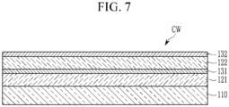
- the examples in fig.7 and fig.8 are not falling under the scope of protection. Differences between the respective examples in FIG. 7 , FIG. 8 and FIG. 9 and the above-described exemplary embodiment of FIG. 6 will be mainly described.
- the cover window CW includes a polymer film 110, and a first hard coating layer 121, a first inorganic layer 131, a second hard coating layer 122, and a second inorganic layer 132 that are sequentially stacked on the polymer film 110.
- the first hard coating layer 121 contacts a top side of the polymer film 110
- the first inorganic layer 131 contacts a top side of the first hard coating layer 121
- the second hard coating layer 122 contacts a top side of the first inorganic layer 131
- the second inorganic layer 132 contacts a top side of the second hard coating layer 122.
- the second hard coating layer 122 is disposed facing the first hard coating layer 121 with the first inorganic layer 131 therebetween, and the second inorganic layer 132 is disposed facing the polymer film 110 with each of the first hard coating layer 121, the first inorganic layer 131 and the second hard coating layer 122 therebetween.
- the polymer film 110 may be provided on the lowest side, and the second inorganic layer 132 may be provided on the highest side.
- the first and second hard coating layers 121 and 122 may be organic layers. Accordingly, the cover window CW may have a structure in which an organic layer and an inorganic layer are alternately stacked on the polymer film 110. These layers may be provided in order from the polymer film 110 in a direction away from the display panel DP. The organic layer and the inorganic layer alternately stacked on the polymer film 110 reduces deformation of the cover window CW and increases surface rigidity may thereof.
- the first and second inorganic layers 131 and 132 may respectively have a thickness of several to several tens of nanometers. A thickness of each of the first and second inorganic layers 131 and 132 may be, for example, equal to or greater than about 5 nm.
- the cover window CW includes a polymer film 110, and a hard coating layer 120, a first inorganic layer 131, and a second inorganic layer 132 that are sequentially stacked on the polymer film 110.
- the first and second inorganic layers 131 and 132 are stacked in order from the hard coating layer 120. That is, the hard coating layer 120, the first inorganic layer 131 and the second inorganic layer 132 are in order from the polymer film 110.
- One relatively thick inorganic layer is provided or formed by a collection of the first and second inorganic layers 131 and 132.
- the first and second inorganic layers 131 and 132 may be provided or formed by more than one deposition process.
- the cover window CW includes an anti-fingerprint layer 140 on the first inorganic layer 131 in comparison to the cover window CW of FIG. 6 .
- the cover window CW may be exposed to outside the display device 1 and may be touched by a user's finger.
- the anti-fingerprint layer 140 may form a top surface of the cover window CW which may be used as a touch side for a touch sensor.
- the anti-fingerprint layer 140 provides abrasion resistance and/or chemical resistance to the cover window CW.
- the anti-fingerprint layer 140 is disposed facing the polymer film 110 with the hard coating layer 120 and the first inorganic layer 131 therebetween, the second inorganic layer 132 defines a bottom outer surface of the cover window CW, and the anti-fingerprint layer 140 defines a top outer surface of the cover window CW which is opposite to the bottom outer surface thereof.
- the cover window CW of FIG. 7 and FIG. 8 may further include an anti-fingerprint layer 140 on the second inorganic layer 132.
- the anti-fingerprint layer 140 may have a thickness of equal to or less than several hundreds of nanometers. In an exemplary embodiment, for example, the thickness of the anti-fingerprint layer 140 may be equal to or less than about 300 nm.
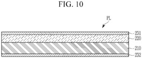
- FIG. 10 shows a cross-sectional view of an exemplary embodiment of a protection layer PL.
- the protection layer PL may be provided on the cover window CW.
- the protection layer PL may be attached to the cover window CW so as to protect the cover window CW that may be relatively expensive.
- the protection layer PL may include a base film 210 and a hard coating layer 220 (e.g., a protection hard coating layer 220) provided thereon.
- the base film 210 may be a polymer film including or made of a polymer such as polyethylene terephthalate (“PET”), polycarbonate (“PC”), or polymethyl methacrylate (“PMMA”).
- the protection layer PL may include a first inorganic layer 231 on the hard coating layer 220, and a second inorganic layer 232 below the base film 210.
- the first inorganic layer 231 and the second inorganic layer 232 may be positioned relative to the base film 210, in one or more of the configurations of the first inorganic layer 131 and the second inorganic layer 132 positioned relative to the polymer film 110 discussed above. Referring to FIG. 10 , along with FIG. 6 , FIG. 7 , FIG. 8 , and FIG.
- the protection layer PL includes inorganic layers 231 and 232 at a same side or at respective opposing sides relative to the base film 210, deformation of the bending area BA of the display device 1 may be reduced, and the surface rigidity may be increased.
- a configuration of the display panel DP included by the display device 1 will now be described with reference to FIG. 11 with the focus on the display area DA.
- FIG. 11 shows a cross-sectional view of an example of a display panel DP.
- FIG. 11 shows an enlarged cross-sectional view of a stacking structure of the display panel DP.
- the cross-section shown in FIG. 11 may correspond to one pixel PX.
Landscapes
- Engineering & Computer Science (AREA)
- Physics & Mathematics (AREA)
- General Physics & Mathematics (AREA)
- Theoretical Computer Science (AREA)
- Computer Hardware Design (AREA)
- Nonlinear Science (AREA)
- Optics & Photonics (AREA)
- Chemical & Material Sciences (AREA)
- General Engineering & Computer Science (AREA)
- Human Computer Interaction (AREA)
- Crystallography & Structural Chemistry (AREA)
- Mathematical Physics (AREA)
- Signal Processing (AREA)
- Devices For Indicating Variable Information By Combining Individual Elements (AREA)
- Inorganic Chemistry (AREA)
- Life Sciences & Earth Sciences (AREA)
- Materials Engineering (AREA)
- Wood Science & Technology (AREA)
- Organic Chemistry (AREA)
- Microelectronics & Electronic Packaging (AREA)
- Electroluminescent Light Sources (AREA)
Claims (5)
- Abdeckfenster (CW), umfassend:eine Polymerfolie (110);eine harte Beschichtungsschicht (120) auf der Polymerfolie (110);eine erste anorganische Schicht (131), die der Polymerfolie (110) zugewandt ist, mit der harten Beschichtungsschicht (120) dazwischen; undeine zweite anorganische Schicht (132) auf der Polymerfolie (110), die eine Außenfläche des Abdeckfensters (CW) definiert,wobei die erste anorganische Schicht (131) und die zweite anorganische Schicht (132) ein Siliziumoxid oder ein Siliziumnitrid beinhalten,wobeidie harte Beschichtungsschicht (120) ein organisches Material beinhaltet,die Polymerfolie (110) eine erste Seite und eine zweite Seite beinhaltet, die einander entlang einer Dicke des Abdeckfensters (CW) gegenüberliegen,die harte Beschichtungsschicht (120) und die erste anorganische Schicht (131) von der ersten Seite der Polymerfolie (110) in der richtigen Reihenfolge angeordnet sind unddie zweite anorganische Schicht (132) die zweite Seite der Polymerfolie (110) berührt,wobei die erste und die zweite anorganische Schicht (131, 132) an jeweiligen gegenüberliegenden Seiten des Abdeckfensters (CW) angeordnet sind.
- Abdeckfenster (CW) nach Anspruch 1, wobei jede der ersten anorganischen Schicht (131) und der zweiten anorganischen Schicht (132) eine Dicke von 5 Nanometern bis 30 Nanometern aufweist.
- Abdeckfenster (CW) nach mindestens einem der Ansprüche 1 bis 2, ferner umfassend eine Anti-Fingerabdruck-Schicht (140), die der Polymerfolie (110) zugewandt ist, mit der harten Beschichtungsschicht (120) und der ersten anorganischen Schicht (131) dazwischen,
wobeidie zweite anorganische Schicht (132) eine untere Außenfläche des Abdeckfensters (CW) definiert unddie Anti-Fingerabdruck-Schicht (140) eine obere Außenfläche des Abdeckfensters (CW) definiert, die der unteren Außenfläche davon gegenüberliegt. - Abdeckfenster (CW) nach mindestens einem der Ansprüche 1 bis 3, wobei die harte Beschichtungsschicht (120) eine Dicke von etwa 10 Mikrometern oder weniger aufweist.
- Abdeckfenster (CW) nach mindestens einem der Ansprüche 1 bis 4, wobei die Polymerfolie (110) ein Polyimid, Polyamid, Polyethylenterephthalat, Polyethylennaphthalat, Polycarbonat oder Polystyrol beinhaltet.
Applications Claiming Priority (1)
| Application Number | Priority Date | Filing Date | Title |
|---|---|---|---|
| KR1020190096737A KR102956597B1 (ko) | 2019-08-08 | 커버 윈도우 및 이를 포함하는 플렉서블 표시 장치 |
Publications (3)
| Publication Number | Publication Date |
|---|---|
| EP3772666A2 EP3772666A2 (de) | 2021-02-10 |
| EP3772666A3 EP3772666A3 (de) | 2021-04-07 |
| EP3772666B1 true EP3772666B1 (de) | 2025-04-02 |
Family
ID=71948468
Family Applications (1)
| Application Number | Title | Priority Date | Filing Date |
|---|---|---|---|
| EP20189332.8A Active EP3772666B1 (de) | 2019-08-08 | 2020-08-04 | Abdeckfenster und flexible anzeigevorrichtung damit |
Country Status (3)
| Country | Link |
|---|---|
| US (1) | US20210041601A1 (de) |
| EP (1) | EP3772666B1 (de) |
| CN (1) | CN112349862A (de) |
Families Citing this family (13)
| Publication number | Priority date | Publication date | Assignee | Title |
|---|---|---|---|---|
| KR102733093B1 (ko) * | 2019-04-16 | 2024-11-25 | 삼성디스플레이 주식회사 | 표시장치 및 이의 제조 방법 |
| JP7598888B2 (ja) * | 2019-06-26 | 2024-12-12 | アプライド マテリアルズ インコーポレイテッド | 折り畳み式ディスプレイ用の可撓性多層カバーレンズ積層体 |
| US11227514B2 (en) * | 2019-12-06 | 2022-01-18 | Wuhan China Star Optoelectronics Semiconductor Display Technology Co., Ltd. | Cover, manufacturing method of cover, and display device |
| WO2021240808A1 (ja) * | 2020-05-29 | 2021-12-02 | シャープ株式会社 | 表示装置 |
| KR20210156917A (ko) * | 2020-06-18 | 2021-12-28 | 삼성디스플레이 주식회사 | 윈도우 및 이를 포함하는 표시 장치 |
| KR102815961B1 (ko) * | 2020-06-22 | 2025-06-05 | 삼성디스플레이 주식회사 | 표시장치 |
| KR102805694B1 (ko) * | 2020-06-24 | 2025-05-14 | 삼성디스플레이 주식회사 | 표시 장치 |
| CN111627337B (zh) * | 2020-06-28 | 2021-12-03 | 武汉华星光电半导体显示技术有限公司 | 折叠显示面板 |
| KR102870269B1 (ko) * | 2020-10-12 | 2025-10-15 | 삼성디스플레이 주식회사 | 전자 장치 |
| KR20220132720A (ko) * | 2021-03-23 | 2022-10-04 | 삼성디스플레이 주식회사 | 표시장치 |
| KR102849486B1 (ko) | 2021-09-30 | 2025-08-25 | 삼성디스플레이 주식회사 | 표시 장치 |
| CN114464090B (zh) * | 2022-01-26 | 2023-02-28 | 武汉华星光电半导体显示技术有限公司 | 显示装置 |
| KR20240029633A (ko) * | 2022-08-25 | 2024-03-06 | 삼성디스플레이 주식회사 | 표시장치 및 이를 포함하는 전자장치 |
Family Cites Families (11)
| Publication number | Priority date | Publication date | Assignee | Title |
|---|---|---|---|---|
| JPS6017421A (ja) * | 1983-07-09 | 1985-01-29 | Konishiroku Photo Ind Co Ltd | 透明導電性フイルム |
| US20040052975A1 (en) * | 2002-04-18 | 2004-03-18 | Minoru Komada | Barrier film and laminated material, container for wrapping and image display medium using the same, and manufacturing method for barrier film |
| US20120301730A1 (en) * | 2011-05-23 | 2012-11-29 | Samsung Electronics Co. Ltd. | Barrier film for an electronic device, methods of manufacturing the same, and articles including the same |
| KR20120130683A (ko) * | 2011-05-23 | 2012-12-03 | 삼성전자주식회사 | 전자 디바이스용 배리어 필름 |
| KR102067416B1 (ko) * | 2012-12-27 | 2020-01-17 | 엘지디스플레이 주식회사 | 내지문-하드 코팅 수지 조성물 및 이를 이용한 내지문-하드 코팅층의 제조 방법 |
| KR102164592B1 (ko) * | 2013-10-24 | 2020-10-13 | 삼성디스플레이 주식회사 | 접이식 표시 장치 |
| KR102260184B1 (ko) * | 2014-02-26 | 2021-06-04 | 삼성디스플레이 주식회사 | 커버 윈도우 및 이를 포함하는 표시 장치 |
| US9790593B2 (en) * | 2014-08-01 | 2017-10-17 | Corning Incorporated | Scratch-resistant materials and articles including the same |
| KR102356723B1 (ko) * | 2015-03-25 | 2022-01-27 | 삼성디스플레이 주식회사 | 커버 윈도우 및 이를 포함하는 표시 장치 |
| KR20170064103A (ko) * | 2015-11-30 | 2017-06-09 | 삼성디스플레이 주식회사 | 커버 윈도우, 이를 포함하는 표시 장치 및 커버 윈도우의 제조 방법 |
| KR20170073948A (ko) * | 2015-12-21 | 2017-06-29 | 삼성전자주식회사 | 플렉서블 필름 구조물 및 그 제조 방법, 및 이를 이용하는 플렉서블 표시 장치 |
-
2020
- 2020-04-13 US US16/846,482 patent/US20210041601A1/en not_active Abandoned
- 2020-08-04 EP EP20189332.8A patent/EP3772666B1/de active Active
- 2020-08-05 CN CN202010775761.XA patent/CN112349862A/zh active Pending
Also Published As
| Publication number | Publication date |
|---|---|
| CN112349862A (zh) | 2021-02-09 |
| EP3772666A2 (de) | 2021-02-10 |
| US20210041601A1 (en) | 2021-02-11 |
| KR20210018674A (ko) | 2021-02-18 |
| EP3772666A3 (de) | 2021-04-07 |
Similar Documents
| Publication | Publication Date | Title |
|---|---|---|
| EP3772666B1 (de) | Abdeckfenster und flexible anzeigevorrichtung damit | |
| US12379620B2 (en) | Flexible display device | |
| US11108014B2 (en) | Flexible display device | |
| CN111462626B (zh) | 可折叠显示装置 | |
| US9417746B2 (en) | Touch-panel substrate | |
| CN105320382B (zh) | 具有触摸面板的柔性显示装置 | |
| KR20200022064A (ko) | 표시 장치 | |
| US20140049892A1 (en) | Touch panel and touch display panel | |
| US11277926B2 (en) | Display device | |
| US10437086B2 (en) | Flexible display device comprising a bendable section in a part of a sealant | |
| US11683949B2 (en) | Flexible cover window and foldable display apparatus | |
| US11917848B2 (en) | Protective window including protected edge glass substrate | |
| CN118135896A (zh) | 显示装置 | |
| KR102956597B1 (ko) | 커버 윈도우 및 이를 포함하는 플렉서블 표시 장치 | |
| US20240224722A1 (en) | Cover module and display device including the same | |
| US20260007042A1 (en) | Display device | |
| US20250261539A1 (en) | Display device | |
| KR20250024580A (ko) | 표시 장치 | |
| KR20250082033A (ko) | 표시 장치 |
Legal Events
| Date | Code | Title | Description |
|---|---|---|---|
| PUAI | Public reference made under article 153(3) epc to a published international application that has entered the european phase |
Free format text: ORIGINAL CODE: 0009012 |
|
| STAA | Information on the status of an ep patent application or granted ep patent |
Free format text: STATUS: THE APPLICATION HAS BEEN PUBLISHED |
|
| AK | Designated contracting states |
Kind code of ref document: A2 Designated state(s): AL AT BE BG CH CY CZ DE DK EE ES FI FR GB GR HR HU IE IS IT LI LT LU LV MC MK MT NL NO PL PT RO RS SE SI SK SM TR |
|
| AX | Request for extension of the european patent |
Extension state: BA ME |
|
| PUAL | Search report despatched |
Free format text: ORIGINAL CODE: 0009013 |
|
| AK | Designated contracting states |
Kind code of ref document: A3 Designated state(s): AL AT BE BG CH CY CZ DE DK EE ES FI FR GB GR HR HU IE IS IT LI LT LU LV MC MK MT NL NO PL PT RO RS SE SI SK SM TR |
|
| AX | Request for extension of the european patent |
Extension state: BA ME |
|
| RIC1 | Information provided on ipc code assigned before grant |
Ipc: G02F 1/1333 20060101ALI20210301BHEP Ipc: B32B 27/00 20060101ALI20210301BHEP Ipc: G06F 1/16 20060101ALI20210301BHEP Ipc: G02B 1/14 20150101AFI20210301BHEP Ipc: H04M 1/02 20060101ALI20210301BHEP |
|
| STAA | Information on the status of an ep patent application or granted ep patent |
Free format text: STATUS: REQUEST FOR EXAMINATION WAS MADE |
|
| 17P | Request for examination filed |
Effective date: 20210824 |
|
| RBV | Designated contracting states (corrected) |
Designated state(s): AL AT BE BG CH CY CZ DE DK EE ES FI FR GB GR HR HU IE IS IT LI LT LU LV MC MK MT NL NO PL PT RO RS SE SI SK SM TR |
|
| STAA | Information on the status of an ep patent application or granted ep patent |
Free format text: STATUS: EXAMINATION IS IN PROGRESS |
|
| 17Q | First examination report despatched |
Effective date: 20230322 |
|
| P01 | Opt-out of the competence of the unified patent court (upc) registered |
Effective date: 20230516 |
|
| GRAP | Despatch of communication of intention to grant a patent |
Free format text: ORIGINAL CODE: EPIDOSNIGR1 |
|
| STAA | Information on the status of an ep patent application or granted ep patent |
Free format text: STATUS: GRANT OF PATENT IS INTENDED |
|
| INTG | Intention to grant announced |
Effective date: 20241030 |
|
| RAP3 | Party data changed (applicant data changed or rights of an application transferred) |
Owner name: SAMSUNG DISPLAY CO., LTD. |
|
| GRAS | Grant fee paid |
Free format text: ORIGINAL CODE: EPIDOSNIGR3 |
|
| GRAA | (expected) grant |
Free format text: ORIGINAL CODE: 0009210 |
|
| STAA | Information on the status of an ep patent application or granted ep patent |
Free format text: STATUS: THE PATENT HAS BEEN GRANTED |
|
| AK | Designated contracting states |
Kind code of ref document: B1 Designated state(s): AL AT BE BG CH CY CZ DE DK EE ES FI FR GB GR HR HU IE IS IT LI LT LU LV MC MK MT NL NO PL PT RO RS SE SI SK SM TR |
|
| REG | Reference to a national code |
Ref country code: GB Ref legal event code: FG4D |
|
| REG | Reference to a national code |
Ref country code: CH Ref legal event code: EP |
|
| REG | Reference to a national code |
Ref country code: IE Ref legal event code: FG4D |
|
| REG | Reference to a national code |
Ref country code: DE Ref legal event code: R096 Ref document number: 602020048620 Country of ref document: DE |
|
| REG | Reference to a national code |
Ref country code: NL Ref legal event code: FP |
|
| PGFP | Annual fee paid to national office [announced via postgrant information from national office to epo] |
Ref country code: NL Payment date: 20250722 Year of fee payment: 6 |
|
| REG | Reference to a national code |
Ref country code: AT Ref legal event code: MK05 Ref document number: 1781792 Country of ref document: AT Kind code of ref document: T Effective date: 20250402 |
|
| PG25 | Lapsed in a contracting state [announced via postgrant information from national office to epo] |
Ref country code: FI Free format text: LAPSE BECAUSE OF FAILURE TO SUBMIT A TRANSLATION OF THE DESCRIPTION OR TO PAY THE FEE WITHIN THE PRESCRIBED TIME-LIMIT Effective date: 20250402 Ref country code: PT Free format text: LAPSE BECAUSE OF FAILURE TO SUBMIT A TRANSLATION OF THE DESCRIPTION OR TO PAY THE FEE WITHIN THE PRESCRIBED TIME-LIMIT Effective date: 20250804 Ref country code: ES Free format text: LAPSE BECAUSE OF FAILURE TO SUBMIT A TRANSLATION OF THE DESCRIPTION OR TO PAY THE FEE WITHIN THE PRESCRIBED TIME-LIMIT Effective date: 20250402 |
|
| PGFP | Annual fee paid to national office [announced via postgrant information from national office to epo] |
Ref country code: DE Payment date: 20250721 Year of fee payment: 6 |
|
| REG | Reference to a national code |
Ref country code: LT Ref legal event code: MG9D |
|
| PG25 | Lapsed in a contracting state [announced via postgrant information from national office to epo] |
Ref country code: NO Free format text: LAPSE BECAUSE OF FAILURE TO SUBMIT A TRANSLATION OF THE DESCRIPTION OR TO PAY THE FEE WITHIN THE PRESCRIBED TIME-LIMIT Effective date: 20250702 Ref country code: GR Free format text: LAPSE BECAUSE OF FAILURE TO SUBMIT A TRANSLATION OF THE DESCRIPTION OR TO PAY THE FEE WITHIN THE PRESCRIBED TIME-LIMIT Effective date: 20250703 |
|
| PG25 | Lapsed in a contracting state [announced via postgrant information from national office to epo] |
Ref country code: PL Free format text: LAPSE BECAUSE OF FAILURE TO SUBMIT A TRANSLATION OF THE DESCRIPTION OR TO PAY THE FEE WITHIN THE PRESCRIBED TIME-LIMIT Effective date: 20250402 |
|
| PG25 | Lapsed in a contracting state [announced via postgrant information from national office to epo] |
Ref country code: BG Free format text: LAPSE BECAUSE OF FAILURE TO SUBMIT A TRANSLATION OF THE DESCRIPTION OR TO PAY THE FEE WITHIN THE PRESCRIBED TIME-LIMIT Effective date: 20250402 |
|
| PGFP | Annual fee paid to national office [announced via postgrant information from national office to epo] |
Ref country code: GB Payment date: 20250722 Year of fee payment: 6 |
|
| PG25 | Lapsed in a contracting state [announced via postgrant information from national office to epo] |
Ref country code: HR Free format text: LAPSE BECAUSE OF FAILURE TO SUBMIT A TRANSLATION OF THE DESCRIPTION OR TO PAY THE FEE WITHIN THE PRESCRIBED TIME-LIMIT Effective date: 20250402 |
|
| PG25 | Lapsed in a contracting state [announced via postgrant information from national office to epo] |
Ref country code: AT Free format text: LAPSE BECAUSE OF FAILURE TO SUBMIT A TRANSLATION OF THE DESCRIPTION OR TO PAY THE FEE WITHIN THE PRESCRIBED TIME-LIMIT Effective date: 20250402 |
|
| PGFP | Annual fee paid to national office [announced via postgrant information from national office to epo] |
Ref country code: FR Payment date: 20250725 Year of fee payment: 6 |
|
| PG25 | Lapsed in a contracting state [announced via postgrant information from national office to epo] |
Ref country code: RS Free format text: LAPSE BECAUSE OF FAILURE TO SUBMIT A TRANSLATION OF THE DESCRIPTION OR TO PAY THE FEE WITHIN THE PRESCRIBED TIME-LIMIT Effective date: 20250702 |
|
| PG25 | Lapsed in a contracting state [announced via postgrant information from national office to epo] |
Ref country code: IS Free format text: LAPSE BECAUSE OF FAILURE TO SUBMIT A TRANSLATION OF THE DESCRIPTION OR TO PAY THE FEE WITHIN THE PRESCRIBED TIME-LIMIT Effective date: 20250802 |
|
| PG25 | Lapsed in a contracting state [announced via postgrant information from national office to epo] |
Ref country code: LV Free format text: LAPSE BECAUSE OF FAILURE TO SUBMIT A TRANSLATION OF THE DESCRIPTION OR TO PAY THE FEE WITHIN THE PRESCRIBED TIME-LIMIT Effective date: 20250402 |
|
| REG | Reference to a national code |
Ref country code: DE Ref legal event code: R097 Ref document number: 602020048620 Country of ref document: DE |
|
| PG25 | Lapsed in a contracting state [announced via postgrant information from national office to epo] |
Ref country code: SM Free format text: LAPSE BECAUSE OF FAILURE TO SUBMIT A TRANSLATION OF THE DESCRIPTION OR TO PAY THE FEE WITHIN THE PRESCRIBED TIME-LIMIT Effective date: 20250402 Ref country code: DK Free format text: LAPSE BECAUSE OF FAILURE TO SUBMIT A TRANSLATION OF THE DESCRIPTION OR TO PAY THE FEE WITHIN THE PRESCRIBED TIME-LIMIT Effective date: 20250402 |
|
| PG25 | Lapsed in a contracting state [announced via postgrant information from national office to epo] |
Ref country code: CZ Free format text: LAPSE BECAUSE OF FAILURE TO SUBMIT A TRANSLATION OF THE DESCRIPTION OR TO PAY THE FEE WITHIN THE PRESCRIBED TIME-LIMIT Effective date: 20250402 |
|
| PG25 | Lapsed in a contracting state [announced via postgrant information from national office to epo] |
Ref country code: EE Free format text: LAPSE BECAUSE OF FAILURE TO SUBMIT A TRANSLATION OF THE DESCRIPTION OR TO PAY THE FEE WITHIN THE PRESCRIBED TIME-LIMIT Effective date: 20250402 |
|
| PG25 | Lapsed in a contracting state [announced via postgrant information from national office to epo] |
Ref country code: RO Free format text: LAPSE BECAUSE OF FAILURE TO SUBMIT A TRANSLATION OF THE DESCRIPTION OR TO PAY THE FEE WITHIN THE PRESCRIBED TIME-LIMIT Effective date: 20250402 Ref country code: SK Free format text: LAPSE BECAUSE OF FAILURE TO SUBMIT A TRANSLATION OF THE DESCRIPTION OR TO PAY THE FEE WITHIN THE PRESCRIBED TIME-LIMIT Effective date: 20250402 |
|
| PG25 | Lapsed in a contracting state [announced via postgrant information from national office to epo] |
Ref country code: IT Free format text: LAPSE BECAUSE OF FAILURE TO SUBMIT A TRANSLATION OF THE DESCRIPTION OR TO PAY THE FEE WITHIN THE PRESCRIBED TIME-LIMIT Effective date: 20250402 |
|
| PLBE | No opposition filed within time limit |
Free format text: ORIGINAL CODE: 0009261 |
|
| STAA | Information on the status of an ep patent application or granted ep patent |
Free format text: STATUS: NO OPPOSITION FILED WITHIN TIME LIMIT |
|
| REG | Reference to a national code |
Ref country code: CH Ref legal event code: L10 Free format text: ST27 STATUS EVENT CODE: U-0-0-L10-L00 (AS PROVIDED BY THE NATIONAL OFFICE) Effective date: 20260211 |
|
| 26N | No opposition filed |
Effective date: 20260105 |
|
| REG | Reference to a national code |
Ref country code: CH Ref legal event code: H13 Free format text: ST27 STATUS EVENT CODE: U-0-0-H10-H13 (AS PROVIDED BY THE NATIONAL OFFICE) Effective date: 20260324 |
|
| PG25 | Lapsed in a contracting state [announced via postgrant information from national office to epo] |
Ref country code: MC Free format text: LAPSE BECAUSE OF FAILURE TO SUBMIT A TRANSLATION OF THE DESCRIPTION OR TO PAY THE FEE WITHIN THE PRESCRIBED TIME-LIMIT Effective date: 20250402 |
|
| PG25 | Lapsed in a contracting state [announced via postgrant information from national office to epo] |
Ref country code: LU Free format text: LAPSE BECAUSE OF NON-PAYMENT OF DUE FEES Effective date: 20250804 |
|
| PG25 | Lapsed in a contracting state [announced via postgrant information from national office to epo] |
Ref country code: CH Free format text: LAPSE BECAUSE OF NON-PAYMENT OF DUE FEES Effective date: 20250831 |