EP3770945B1 - Detektor von kikuchi-beugung - Google Patents
Detektor von kikuchi-beugung Download PDFInfo
- Publication number
- EP3770945B1 EP3770945B1 EP19188579.7A EP19188579A EP3770945B1 EP 3770945 B1 EP3770945 B1 EP 3770945B1 EP 19188579 A EP19188579 A EP 19188579A EP 3770945 B1 EP3770945 B1 EP 3770945B1
- Authority
- EP
- European Patent Office
- Prior art keywords
- detector
- mounting portion
- body mounting
- head
- sem
- Prior art date
- Legal status (The legal status is an assumption and is not a legal conclusion. Google has not performed a legal analysis and makes no representation as to the accuracy of the status listed.)
- Active
Links
Images

Classifications
-
- G—PHYSICS
- G01—MEASURING; TESTING
- G01N—INVESTIGATING OR ANALYSING MATERIALS BY DETERMINING THEIR CHEMICAL OR PHYSICAL PROPERTIES
- G01N23/00—Investigating or analysing materials by the use of wave or particle radiation, e.g. X-rays or neutrons, not covered by groups G01N3/00 – G01N17/00, G01N21/00 or G01N22/00
- G01N23/20—Investigating or analysing materials by the use of wave or particle radiation, e.g. X-rays or neutrons, not covered by groups G01N3/00 – G01N17/00, G01N21/00 or G01N22/00 by using diffraction of the radiation by the materials, e.g. for investigating crystal structure; by using scattering of the radiation by the materials, e.g. for investigating non-crystalline materials; by using reflection of the radiation by the materials
- G01N23/207—Diffractometry using detectors, e.g. using a probe in a central position and one or more displaceable detectors in circumferential positions
-
- G—PHYSICS
- G01—MEASURING; TESTING
- G01N—INVESTIGATING OR ANALYSING MATERIALS BY DETERMINING THEIR CHEMICAL OR PHYSICAL PROPERTIES
- G01N23/00—Investigating or analysing materials by the use of wave or particle radiation, e.g. X-rays or neutrons, not covered by groups G01N3/00 – G01N17/00, G01N21/00 or G01N22/00
- G01N23/02—Investigating or analysing materials by the use of wave or particle radiation, e.g. X-rays or neutrons, not covered by groups G01N3/00 – G01N17/00, G01N21/00 or G01N22/00 by transmitting the radiation through the material
- G01N23/04—Investigating or analysing materials by the use of wave or particle radiation, e.g. X-rays or neutrons, not covered by groups G01N3/00 – G01N17/00, G01N21/00 or G01N22/00 by transmitting the radiation through the material and forming images of the material
-
- G—PHYSICS
- G01—MEASURING; TESTING
- G01N—INVESTIGATING OR ANALYSING MATERIALS BY DETERMINING THEIR CHEMICAL OR PHYSICAL PROPERTIES
- G01N23/00—Investigating or analysing materials by the use of wave or particle radiation, e.g. X-rays or neutrons, not covered by groups G01N3/00 – G01N17/00, G01N21/00 or G01N22/00
- G01N23/20—Investigating or analysing materials by the use of wave or particle radiation, e.g. X-rays or neutrons, not covered by groups G01N3/00 – G01N17/00, G01N21/00 or G01N22/00 by using diffraction of the radiation by the materials, e.g. for investigating crystal structure; by using scattering of the radiation by the materials, e.g. for investigating non-crystalline materials; by using reflection of the radiation by the materials
- G01N23/20058—Measuring diffraction of electrons, e.g. low energy electron diffraction [LEED] method or reflection high energy electron diffraction [RHEED] method
-
- G—PHYSICS
- G01—MEASURING; TESTING
- G01N—INVESTIGATING OR ANALYSING MATERIALS BY DETERMINING THEIR CHEMICAL OR PHYSICAL PROPERTIES
- G01N23/00—Investigating or analysing materials by the use of wave or particle radiation, e.g. X-rays or neutrons, not covered by groups G01N3/00 – G01N17/00, G01N21/00 or G01N22/00
- G01N23/20—Investigating or analysing materials by the use of wave or particle radiation, e.g. X-rays or neutrons, not covered by groups G01N3/00 – G01N17/00, G01N21/00 or G01N22/00 by using diffraction of the radiation by the materials, e.g. for investigating crystal structure; by using scattering of the radiation by the materials, e.g. for investigating non-crystalline materials; by using reflection of the radiation by the materials
- G01N23/203—Measuring back scattering
-
- G—PHYSICS
- G01—MEASURING; TESTING
- G01N—INVESTIGATING OR ANALYSING MATERIALS BY DETERMINING THEIR CHEMICAL OR PHYSICAL PROPERTIES
- G01N23/00—Investigating or analysing materials by the use of wave or particle radiation, e.g. X-rays or neutrons, not covered by groups G01N3/00 – G01N17/00, G01N21/00 or G01N22/00
- G01N23/20—Investigating or analysing materials by the use of wave or particle radiation, e.g. X-rays or neutrons, not covered by groups G01N3/00 – G01N17/00, G01N21/00 or G01N22/00 by using diffraction of the radiation by the materials, e.g. for investigating crystal structure; by using scattering of the radiation by the materials, e.g. for investigating non-crystalline materials; by using reflection of the radiation by the materials
- G01N23/2055—Analysing diffraction patterns
-
- G—PHYSICS
- G01—MEASURING; TESTING
- G01N—INVESTIGATING OR ANALYSING MATERIALS BY DETERMINING THEIR CHEMICAL OR PHYSICAL PROPERTIES
- G01N23/00—Investigating or analysing materials by the use of wave or particle radiation, e.g. X-rays or neutrons, not covered by groups G01N3/00 – G01N17/00, G01N21/00 or G01N22/00
- G01N23/22—Investigating or analysing materials by the use of wave or particle radiation, e.g. X-rays or neutrons, not covered by groups G01N3/00 – G01N17/00, G01N21/00 or G01N22/00 by measuring secondary emission from the material
- G01N23/2206—Combination of two or more measurements, at least one measurement being that of secondary emission, e.g. combination of secondary electron [SE] measurement and back-scattered electron [BSE] measurement
-
- G—PHYSICS
- G01—MEASURING; TESTING
- G01N—INVESTIGATING OR ANALYSING MATERIALS BY DETERMINING THEIR CHEMICAL OR PHYSICAL PROPERTIES
- G01N23/00—Investigating or analysing materials by the use of wave or particle radiation, e.g. X-rays or neutrons, not covered by groups G01N3/00 – G01N17/00, G01N21/00 or G01N22/00
- G01N23/22—Investigating or analysing materials by the use of wave or particle radiation, e.g. X-rays or neutrons, not covered by groups G01N3/00 – G01N17/00, G01N21/00 or G01N22/00 by measuring secondary emission from the material
- G01N23/225—Investigating or analysing materials by the use of wave or particle radiation, e.g. X-rays or neutrons, not covered by groups G01N3/00 – G01N17/00, G01N21/00 or G01N22/00 by measuring secondary emission from the material using electron or ion
- G01N23/2251—Investigating or analysing materials by the use of wave or particle radiation, e.g. X-rays or neutrons, not covered by groups G01N3/00 – G01N17/00, G01N21/00 or G01N22/00 by measuring secondary emission from the material using electron or ion using incident electron beams, e.g. scanning electron microscopy [SEM]
-
- G—PHYSICS
- G01—MEASURING; TESTING
- G01T—MEASUREMENT OF NUCLEAR OR X-RADIATION
- G01T1/00—Measuring X-radiation, gamma radiation, corpuscular radiation, or cosmic radiation
- G01T1/16—Measuring radiation intensity
- G01T1/20—Measuring radiation intensity with scintillation detectors
- G01T1/2006—Measuring radiation intensity with scintillation detectors using a combination of a scintillator and photodetector which measures the means radiation intensity
-
- H—ELECTRICITY
- H01—ELECTRIC ELEMENTS
- H01J—ELECTRIC DISCHARGE TUBES OR DISCHARGE LAMPS
- H01J37/00—Discharge tubes with provision for introducing objects or material to be exposed to the discharge, e.g. for the purpose of examination or processing thereof
- H01J37/02—Details
- H01J37/244—Detectors; Associated components or circuits therefor
-
- H—ELECTRICITY
- H01—ELECTRIC ELEMENTS
- H01J—ELECTRIC DISCHARGE TUBES OR DISCHARGE LAMPS
- H01J37/00—Discharge tubes with provision for introducing objects or material to be exposed to the discharge, e.g. for the purpose of examination or processing thereof
- H01J37/252—Tubes for spot-analysing by electron or ion beams; Microanalysers
- H01J37/256—Tubes for spot-analysing by electron or ion beams; Microanalysers using scanning beams
-
- H—ELECTRICITY
- H01—ELECTRIC ELEMENTS
- H01J—ELECTRIC DISCHARGE TUBES OR DISCHARGE LAMPS
- H01J37/00—Discharge tubes with provision for introducing objects or material to be exposed to the discharge, e.g. for the purpose of examination or processing thereof
- H01J37/26—Electron or ion microscopes; Electron or ion diffraction tubes
- H01J37/28—Electron or ion microscopes; Electron or ion diffraction tubes with scanning beams
-
- H—ELECTRICITY
- H01—ELECTRIC ELEMENTS
- H01J—ELECTRIC DISCHARGE TUBES OR DISCHARGE LAMPS
- H01J37/00—Discharge tubes with provision for introducing objects or material to be exposed to the discharge, e.g. for the purpose of examination or processing thereof
- H01J37/26—Electron or ion microscopes; Electron or ion diffraction tubes
- H01J37/295—Electron or ion diffraction tubes
- H01J37/2955—Electron or ion diffraction tubes using scanning ray
-
- G—PHYSICS
- G01—MEASURING; TESTING
- G01N—INVESTIGATING OR ANALYSING MATERIALS BY DETERMINING THEIR CHEMICAL OR PHYSICAL PROPERTIES
- G01N2223/00—Investigating materials by wave or particle radiation
- G01N2223/03—Investigating materials by wave or particle radiation by transmission
-
- G—PHYSICS
- G01—MEASURING; TESTING
- G01N—INVESTIGATING OR ANALYSING MATERIALS BY DETERMINING THEIR CHEMICAL OR PHYSICAL PROPERTIES
- G01N2223/00—Investigating materials by wave or particle radiation
- G01N2223/045—Investigating materials by wave or particle radiation combination of at least 2 measurements (transmission and scatter)
-
- G—PHYSICS
- G01—MEASURING; TESTING
- G01N—INVESTIGATING OR ANALYSING MATERIALS BY DETERMINING THEIR CHEMICAL OR PHYSICAL PROPERTIES
- G01N2223/00—Investigating materials by wave or particle radiation
- G01N2223/05—Investigating materials by wave or particle radiation by diffraction, scatter or reflection
- G01N2223/053—Investigating materials by wave or particle radiation by diffraction, scatter or reflection back scatter
-
- G—PHYSICS
- G01—MEASURING; TESTING
- G01N—INVESTIGATING OR ANALYSING MATERIALS BY DETERMINING THEIR CHEMICAL OR PHYSICAL PROPERTIES
- G01N2223/00—Investigating materials by wave or particle radiation
- G01N2223/05—Investigating materials by wave or particle radiation by diffraction, scatter or reflection
- G01N2223/056—Investigating materials by wave or particle radiation by diffraction, scatter or reflection diffraction
- G01N2223/0565—Investigating materials by wave or particle radiation by diffraction, scatter or reflection diffraction diffraction of electrons, e.g. LEED
-
- G—PHYSICS
- G01—MEASURING; TESTING
- G01N—INVESTIGATING OR ANALYSING MATERIALS BY DETERMINING THEIR CHEMICAL OR PHYSICAL PROPERTIES
- G01N2223/00—Investigating materials by wave or particle radiation
- G01N2223/07—Investigating materials by wave or particle radiation secondary emission
- G01N2223/071—Investigating materials by wave or particle radiation secondary emission combination of measurements, at least 1 secondary emission
-
- G—PHYSICS
- G01—MEASURING; TESTING
- G01N—INVESTIGATING OR ANALYSING MATERIALS BY DETERMINING THEIR CHEMICAL OR PHYSICAL PROPERTIES
- G01N2223/00—Investigating materials by wave or particle radiation
- G01N2223/50—Detectors
- G01N2223/505—Detectors scintillation
Definitions
- the invention relates to a detector for Kikuchi diffraction, KD, particularly to a compact, lightweight and low-cost KD detector for use with compact SEMs, such as table top SEMs.
- the structure of crystalline materials can be analyzed using diffraction methods, wherein suitable electromagnetic waves are coherently scattered by the atoms of the material.
- the direction-dependent intensity of the scattered radiation is then recorded at different scattering angles.
- Various information on the crystalline material such as on the crystal structure, chemical bonds or mechanical strain within the sample, can be derived from the recorded angle-dependent intensity distribution of the diffracted waves of the applied radiation.
- Suitable radiation can either be electromagnetic radiation, such as X-rays, or massive particle radiation, such as electron or neutron beams, as long as the wavelength of the radiation is within the magnitude of the lattice constant(s) of the structure(s) to be analyzed. While X-ray crystallography still is one of the most widely used techniques in global structure analysis, more methods utilizing electron beams for resolving crystal structures are developed and at least some of these methods can be functionally integrated in SEMs.
- EDS energy dispersive spectroscopy
- Kikuchi diffraction Another analytic technique for measuring crystal orientation that becomes more commonly integrated into electron microscopes.
- This technique can be implemented as electron backscatter diffraction (EBSD), which is also known as backscatter Kikuchi diffraction (BKD), or as transmission Kikuchi diffraction (TKD), also known as transmission electron backscatter diffraction (t-EBSD).
- EBSD electron backscatter diffraction
- BKD backscatter Kikuchi diffraction
- TKD transmission Kikuchi diffraction
- t-EBSD transmission electron backscatter diffraction
- Kikuchi diffraction a crystalline sample is placed in a scanning electron microscope (SEM) and irradiated with a focused electron beam. At least part of the electrons are scattered within the sample and then exit it with an angle-dependent intensity distribution.
- Kikuchi patterns can be recorded in a gnomonic projection on the detector surface and can be analyzed with respect to the crystal orientation and structure of the crystalline sample.
- EBSD the backscatter electrons are detected upstream the sample with respect to a propagation direction of the initially incident electron beam, whereas in TKD transmitted and diffracted electrons are detected downstream the sample in this direction.
- Kikuchi detectors are rather complex and thus require significant mounting space inside and outside the vacuum chamber of an electron microscope. Above that the currently available highly specialized Kikuchi detectors are rather directed to the highest possible versatility and precision and rather not to providing a cost-effective tool for widespread use in different kinds of SEMs.
- US 2003/057377 A1 discloses an EBSD detector that shall allow for minimizing a space occupied in an SEM chamber, wherein the EBSD detector is mounted to a housing of a SEM enclosing the SEM chamber via a SEM port and wherein a scintillation substrate of the detector is mounted to a support shaft, which can be retracted by motor shaft and pivoted upwards for freeing room in the SEM chamber when using of other tools therein.
- An aspect of the present invention relates to a detector for Kikuchi diffraction, particularly for electron backscatter diffraction, EBSD, or for transmission Kikuchi diffraction, TKD.
- the detector of the present invention shall be in principle usable for both of these measurement configurations, which differ mainly by the positioning of the detector surface relative to the sample position. Without being restricted thereto, in the following the detector of the invention is described with respect to EBSD where it is necessary or appropriate to specify this.
- the detector of the present invention comprises a photodetector configured for detecting incident radiation, a detector body and a detector head, which are mountable to each other.
- the detector body and the detector head can be selectively mounted (connected) to each other, i.e., a detachable connection can be formed between the detector body and the detector head.
- a detachable connection can be formed between the detector body and the detector head.
- the detector body comprises a body part which is enclosing a photodetector that is configured for detecting incident radiation.
- the body part forms the main body of the detector body and preferably comprises a housing. Within this housing further components of the detector next to the photodetector might be disposed, particularly control electronics and/or means for cooling the detector.
- the photodetector disposed in the body part, preferably the housing thereof, may be one of a CCD or CMOS photodetector.
- the photodetector comprises at least an active detector surface, e.g., a silicon detector surface, and readout electronics electrically connected to the active detector surface.
- the photodetector is particularly configured to detect Kikuchi pattern and comprises e.g., a size, resolution and/or sensitivity that is suitable for detecting Kikuchi patterns.
- the body part further comprises a vacuum window that is arranged upstream the photodetector with respect to a propagation direction of the incident radiation.
- the vacuum window is configured to seal the body part, particularly the housing with the detector components disposed therein against an exterior environment. In a mounted state of the detector body this exterior environment is a SEM chamber as described below.
- the vacuum window is thus configured to seal the body part from the vacuum in a SEM chamber and vice versa.
- the vacuum window is, at least substantially, transparent and configured to allow the transmittance of incident photons emitted by a scintillation screen of the detector.
- the detector body further comprises a first body mounting portion and a second body mounting portion.
- the first body mounting portion is configured to be mounted to a SEM chamber port of a SEM.
- Common SEMs comprise at least one chamber port for mounting electron microscope accessory, such as detectors, cameras, sample preparation means or the like.
- the geometry and fastening systems of those SEM chamber ports are usually standardized, at least for a given manufacturer.
- the first body mounting portion has a defined configuration. For the skilled person it is a standard task to determine the configuration of the first body mounting portion with respect to a certain SEM and a required mounting quality.
- a SEM chamber port comprises at least one mounting flange, such as e.g., a circular mounting flange, e.g., circumcising a mounting aperture in an outer wall of the SEM.
- the mounting flange may further comprise sealing means, such as e.g., mounting grooves for inserting vacuum seals.
- sealing means such as e.g., mounting grooves for inserting vacuum seals.
- flat vacuum gaskets might be used with the mounting flange.
- the mounting flange usually comprises mounting means, such as e.g., screw holes within the mounting flange.
- other fastening means providing a form and/or force closure between the mounting flange and a mounted component might be used.
- the mounting flange of the chamber port might be external or internal of the SEM outer wall.
- a microscope accessory might also be inserted into an opening of an SEM outer wall and secured therein by a bayonet fastening mechanism and sealing means.
- the first body mounting portion is configured to be mounted to such a SEM chamber port of a SEM.
- the first body mounting portion comprises a first mounting flange that is configured to be mounted to a mounting flange of a SEM chamber port.
- the size of the first mounting flange may be adapted to the size of the mounting flange.
- the positioning of bores, screw holes and/or mounting structures for sealing means may be adapted to the positioning of the corresponding elements on the SEM mounting flange.
- the detector body of the detector of the present invention further comprises a second body mounting portion that is configured to be mounted to the detector head.
- the second body mounting portion realizes the detachable connection mentioned above on side of the detector body.
- the second body mounting portion is thus one part of a connecting mechanism between the detector body and the detector head realizing the modular structure.
- the detector head of the detector of the present invention comprises a head mounting portion that is configured to be mounted to the second body mounting portion.
- the head mounting portion is configured as a counterpart for the second body mounting portion, such that the configurations of both of these elements depend on each other.
- the head mounting portion is mountable to the second body mounting portion for mounting the detector head to the detector body.
- the detachable connection between the head mounting portion and the second body mounting portion realizes the detachable connection between the detector head and the detector body.
- the detachable connection between the head mounting portion and the second body mounting portion is preferably configured to provide a vacuum sealed connection. Therefore, these connection elements are preferably configured to insert sealing means, such as e.g., gaskets therein.
- the detector head of the present invention further comprises a scintillation screen, i.e., a structure that converts incident scattered electrons into electromagnetic radiation, i.e., photons.
- the scintillation screen might comprise a phosphor layer configured to emit photons in response to incident backscattered electrons.
- the scintillation screen is positioned near the sample either upstream (EBSD) or downstream (TKD) with respect to the incident electron beam.
- the scintillation screen is preferably configured to convert the expected dose of incident (back)-scattered electrons into electromagnetic radiation with an intensity and/or a preferred direction of emittance that allows to detect this electromagnetic radiation with a high quantum yield at the photodetector.
- the Kikuchi detector of the present invention can be advantageously used for low end SEMs, particularly with small SEMs comprising a compact SEM chamber.
- This is achieved by providing a Kikuchi detector with a modular structure as described above.
- this structure allows to permanently mount the detector body to the SEM via the first body mounting portion. Then, the detector head can be selectively mounted to the second body mounting portion into to the SEM chamber. That is, in case the Kikuchi detector is not required, the detector head can be removed for freeing space in the SEM chamber.
- the modular structure simplifies maintenance of the Kikuchi detector, e.g., by selectively replacing or maintaining components in the detector body, such as e.g., the photodetector, or components in the detector head, such as e.g., the scintillation screen.
- the first body mounting portion is disposed in between the second mounting portion and the photodetector.
- the first body mounting portion follows on the photodetector and then the second body mounting portion follows on the first body mounting portion.
- the extension direction of the detector body preferably corresponds to a propagation direction of incident radiation, particularly preferred the radiation emitted by the scintillation screen in response to the incident scattered electrons.
- the second body mounting portion extends upstream the first body mounting portion with respect to the propagation direction of the incident radiation emitted by the scintillation screen.
- the first body mounting portion is disposed between the body part and the second body mounting portion and hence the second body mounting portion preferably forms an outermost (or terminal end) of the detector body.
- the first body mounting portion In a lateral direction, i.e., a direction perpendicular the propagation direction of incident radiation (extension direction), the first body mounting portion preferably extends over the second body mounting portion.
- a width of the first body mounting portion exceeds the width of the second body mounting portion in order to allow sealing the SEM chamber port.
- the second body mounting portion is configured to be inserted through the SEM chamber port, before the first body mounting portion is mounted to an outer side of the SEM chamber port.
- the second body mounting portion in order to mount the first body mounting portion to the SEM chamber port, the second body mounting portion has to be inserted into the SEM chamber or at least through the SEM chamber port, depending on a wall thickness of the SEM.
- the lateral extension of the second body mounting portion is less than the lateral extension of the first body mounting portion in order to allow the insertion through the SEM chamber port.
- the second body mounting portion preferably has an extension, e.g., along the propagation direction of the incident radiation, which extends the thickness of the SEM outer wall such that the second body mounting portion extends into the SEM chamber.
- the body part of the detector according to the present invention is disposed outside the SEM chamber, particularly outside the SEM, and the second body mounting portion is disposed inside the SEM chamber and is accessible from inside the SEM chamber.
- the detector head particularly the head mounting portion
- the head mounting portion can be mounted to the detector body, particularly the second body mounting portion thereof, from within the SEM chamber.
- the head mounting portion is configured to be mounted to the second body mounting portion, while the second body mounting portion is inserted through the SEM chamber port, and from an inner side of a SEM chamber. That is, the detector body of the detector according to the invention does not have to be removed from the SEM chamber port for mounting the detector head. This increases the versatility of the SEM for a user as the SEM chamber can be freed when Kikuchi measurements are not required by a user, while the detector body stays mounted.
- the detector head comprises a hollow column, particularly preferred a hollow steel column.
- the hollow column preferably is of a cylindrical shape such as e.g., of a circular cylindrical shape. However, other shapes are possible as long as they allow for transmission of radiation along the already mentioned propagation (extension) direction.
- the head mounting portion is disposed at a first end of the hollow column, i.e., at one terminal end of the hollow column with which the column is mounted to the second body mounting portion of the detector body. Further, the scintillation screen is mounted to a second end of the hollow column opposite the first end.
- the length of the hollow column corresponds to a distance between the side of the SEM chamber port facing the SEM chamber and a sample position.
- the sample position is the position of a sample in the SEM chamber during a measurement of Kikuchi patterns.
- the sample position is preferably determined by a sample stage or sample holder mounted within the SEM chamber.
- the scintillation screen is preferably positioned adjacent the sample position of the SEM chamber, when the first body mounting portion is mounted to the SEM chamber port and when the head mounting portion is mounted to the second body mounting portion.
- the length of the hollow column preferably corresponds to a distance between the side of the SEM chamber port facing the SEM chamber and a sample position so that the scintillation screen receives an optimal yield and distribution of the radiation produced by the sample.
- the scintillation screen is mounted to a screen holder which again is mounted to the hollow column of the detector head, particularly to the second end of the hollow column.
- the detector head comprises a screen holder which is connectable to the hollow column, e.g., the second end thereof, and which is carrying the scintillation screen.
- This embodiment advantageously allows an easy replacement of the scintillation screen by replacing the screen holder.
- the screen holder and the hollow column can be stored separately, which more easily allows for an adequate storage of the very sensitive scintillation screen.
- the length of the hollow column with the screen holder mounted thereto corresponds to the distance between the SEM chamber port and the sample position.
- the second body mounting portion comprises L-shaped reception elements forming a groove with a flange surface of the second body mounting portion. Then, the flange elements are slid into the groove parallely to the flange surface, i.e., along the lateral direction of the detector, e.g. perpendicular to the extension direction. Further preferred, the L-shaped reception elements are fixed to the second body mounting portion with permanently mounted screws. By tightening those screws, the flange elements are then secured by the L-shaped reception elements. According to this embodiment, the detector head can be advantageously mounted to the detector body without inserting additional loose screws into the SEM chamber by simply sliding the head mounting portion of the detector head in the second body mounting portion of the detector body.
- the head mounting portion and/or the second body mounting portion further comprises alignment means for supporting a proper alignment of the head mounting portion and the second body mounting portion.
- the alignment means might comprise spring loaded balls as well as corresponding circular reception apertures, wherein the spring-loaded balls are disposed in the reception apertures, when the detector head is aligned with the detector body.
- one of the detector head and detector body comprises at least one defined end-stop element, providing an end-stop in an alignment position of detector head and detector body. Particularly preferred, such an end-stop is provided by an additional L-shaped element oriented perpendicular to the above mentioned sliding direction.
- the optical system can be distributed to the detector body and the detector head.
- the photodetector is disposed in the detector body while the scintillation screen is disposed in the detector head.
- an objective lens is disposed in the detector body, particularly between the vacuum window and the photodetector of the detector body.
- the objective lens is disposed adjacent to the photodetector. This allows for precisely setting the properties of imaging the incident radiation onto the active surface of the photodetector.
- the detector body particularly preferred the body part of the detector, comprises a fiber optical taper that is positioned upstream the photodetector with respect to the propagation direction of the incident radiation.
- the fiber optical taper is preferably formed by a coherent arrangement of fibers that are arranged in a surface-to-surface arrangement forming a first base surface and a smaller second base surface.
- the first base surface is facing the detector head and an image signal input to the first base surface is transmitted as a reduced image to the second base surface facing the active surface of the photodetector.
- the reduction is defined by a ratio of the first and second base surface.
- the upstream end of the fiber optical taper constitutes the vacuum window and an additional vacuum window can thus be omitted.
- the detector head further comprises a field lens that is arranged adjacent the scintillation screen in the propagation direction of the incident radiation.
- the field lens preferably has a high numerical aperture and allows for capturing a high fraction of the light emitted by the scintillation screen as well as for focusing it on the remaining optical system.
- a planar side of the field lens is facing the scintillation screen and the convexly curved side of the field lens is facing away from the scintillation screen.
- the detector body of the present invention at least comprises a body part, which encloses at least a photodetector configured for detecting incident radiation, particularly incident electromagnetic radiation emitted by a scintillation screen.
- the body part preferably further comprises control electronics of the photodetector and/or of the detector as a whole as well as cooling means for cooling the photodetector and/or the detector as a whole.
- the detector body of the present invention further comprises a vacuum window that is arranged upstream the photodetector with respect to a propagation direction of the incident radiation, particularly with respect to the incident radiation, e.g., emitted by a scintillation screen disposed in the detector head.
- the detector body according to the present invention further comprises a first body mounting portion that is configured to be mounted to a SEM chamber port of a SEM.
- the first body mounting portion preferably comprises a common first mounting flange for mounting a microscope accessory to a SEM via a SEM chamber port.
- the first body mounting portion might comprise a first mounting flange adapted to a mounting flange of the SEM chamber port.
- the detector body further comprises a second body mounting portion that is configured to be mounted to the head mounting portion of the detector head as described above.
- the second body mounting portion comprises at least one reception element configured for guiding, receiving and/or fastening the at least one flange element.
- the second body mounting portion extends upstream the first body mounting portion with respect to the propagation direction of the incident radiation.
- the first body mounting portion is disposed in between the second mounting portion and the photodetector and the first body mounting portion extends laterally above the second body mounting portion.
- another aspect of the present invention relates to a detector head for the detector body of a detector according to claim 1.
- the detector head of the invention comprises at least a hollow column with a first (terminal) end and with a second (terminal) end that is opposite to the first end.
- a head mounting portion is disposed at the first end, comprises at least one flange element and is configured to be mounted to the second body mounting portion of the detector body via the at least one flange element.
- a scintillation screen is mounted to the second end, preferably via a screen holder. Further preferred embodiments of the detector head correspond to those described for the detector.
- another aspect of the present invention relates to a detection system for Kikuchi diffraction, the detection system comprising a scanning electron microscope, SEM, comprising a SEM vacuum chamber and at least one SEM chamber port for accessing the SEM chamber.
- the SEM further comprises an electron source, one or more electron lenses, a sample stage and/or a sample holder, a vacuum system and/or the like.
- the detection system of the invention further comprises a detector according to the present invention as defined in claim 1. Preferred embodiments of the system are set out in claims 11 to 13.
- the first body mounting portion of the detector body is preferably mounted to a SEM chamber port of the SEM such that the second body mounting portion is inserted through the SEM chamber port and extends at least partially into the SEM chamber, when the first body mounting portion is mounted to the SEM chamber port.
- the detector head is preferably mounted via its head mounting portion to the second body mounting portion and is disposed in the SEM chamber.
- first and second are used to describe various elements, these elements should not be limited by these terms. These terms are only used to distinguish one element from another element. For example, a first element may be named a second element and, similarly, a second element may be named a first element, without departing from the scope of the present invention.
- the term “substantially”, “about,” and similar terms are used as terms of approximation and not as terms of degree, and are intended to account for the inherent deviations in measured or calculated values that would be recognized by those of ordinary skill in the art. Further, if the term “substantially” is used in combination with a feature that could be expressed using a numeric value, the term “substantially” denotes a range of +/- 5% of the value centered on the value.
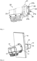
- Figure 1 schematically illustrates a perspective view detector body 20 according to an embodiment.
- the detector body 20 as shown in Figure 1 is designed to be mounted to a detector head 30 as illustrated e.g., in Figure 5 for forming the detector 10 of the invention.
- the detector body 20 of Figure 1 comprises a body part 23, which is a plastic housing for enclosing a photodetector (not shown) as well as control electronics of the photodetector and the detector 10 as whole.
- a heat exchanger comprising a plurality of cooling fins is mounted for dissipating heat emitted by the detector body 20.
- the detector body 20 comprises a first body mounting portion 21 and a second body mounting portion 22 disposed at a terminal end of the body part 23.
- the first body mounting portion 21 is disposed in between the body part 23 and the second body mounting portion 22.
- the first body mounting portion 21 is configured to be mounted to an SEM chamber port 50. Therefore, the first body mounting portion 21 comprises a first mounting flange extending laterally from the body part 23.
- a plurality of connection screws sit in the first mounting flange and are configured and positioned to fit into corresponding screw holes of a mounting flange of the SEM chamber port 50.
- a flat vacuum gasket (not shown) with openings corresponding to the screws is positioned between the first mounting flange and the SEM mounting flange.
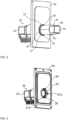
- FIG 2 schematically illustrates an outer perspective view of a detector 10 comprising the detector body 20 of Figure 1 mounted to an SEM chamber port 50 of a SEM.
- the first body mounting portion 21 sits tightly on a mounting flange (not shown) circumferentially surrounding the mounting opening in the SEM chamber port 50.
- the first body mounting portion 21 is fastened to the SEM chamber port 50 by a plurality of screws and a flat vacuum gasket is provided between the SEM chamber port 50 and the first body mounting portion 21.
- the second body mounting portion 22 extends upstream of the first body mounting portion 21 with respect to a propagation direction of an incident radiation.
- the detector body 20 is configured to detect radiation that enters the body part 23 first via a central aperture in the second body mounting portion 22 and subsequently via a central aperture in the first body mounting portion 21.
- the second body mounting portion 22 is of substantially cylindrical shape and has an extension in the propagation direction which exceeds or at least equals the thickness of a SEM chamber wall.
- a first base surface of the cylindrical second body mounting portion 22 is connected to the detector body 20, e.g., to the first body mounting portion 21.
- a second base surface of the cylindrical second body mounting portion 22 opposite the first base surface is facing into the SEM chamber, when the first body mounting portion 21 is mounted to an SEM chamber port 50.
- the second base surface is aligned with an inner surface of the SEM chamber port 50.
- the second base surface of the second body mounting portion 22 and the inner surface of the SEM chamber port 50 form a continuous straight and level surface.
- the second body mounting portion 22 comprises reception elements 26 and alignment elements 27 that both protrude from the second base into the SEM chamber, when the detector body 20 is mounted to the SEM chamber port 50.
- the reception elements 26 are formed by a pair of L-shaped fasteners 26 arranged opposite to each other on the second base surface.
- Each of the L-shaped fasteners 26 comprise a first leg and a second leg perpendicular to the first leg.
- the L-shaped fasteners 26 are mounted to the second base surface with their respective first legs such that their respective second legs extend parallelly to the second base surface.
- the L-shaped fasteners 26 are mounted to the second base surface via screws extending through their respective first legs. Hence, each of the L-shaped fasteners 26 forms a guiding groove between its second leg and the second base surface. Further, the L-shaped fasteners 26 are mounted opposite to each other such that the openings of the guiding grooves are facing each other.
- the head mounting portion 34 of a detector head 30 as e.g., illustrated in Figure 5 particularly the flange elements 37 of such head mounting portion 34, can be slid into the guiding grooves of the fasteners 26 for mounting the detector head 30.
- the second body mounting portion 22 further comprises alignment means 27 that comprise a third L-shaped fastener 27a that is mounted to the second base surface with an orientation perpendicular to that of the L-shaped fasteners 26 mounted as reception elements 26.
- the third L-shaped fastener 27a functions as a defined end-stop for the head mounting portion 34.
- four alignment pins 27b protrude from the second base surface for guiding the head mounting portion 34 into the guiding grooves of the L-shaped fasteners 27a.
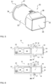
- the scintillation screen 35 mounted to a screen holder 36 is disposed adjacent to a sample position in the SEM chamber in order to detect a large portion of scattered electrons.
- the detector head 30, as shown in detail in Figure 5 is of a length that corresponds to the distance between the SEM chamber port 50, particularly the mounting opening thereof, and a sample position, i.e., a position of a sample in the SEM chamber during Kikuchi measurements.
- the length of the detector head 30 is thereby formed by a hollow column 33 and a screen holder 36 attached thereto.
- the hollow column 33 comprises a first terminal end 31 comprising the head mounting portion 34 configured for mounting the second body mounting portion 22 and a second terminal end 32 opposite the first terminal end.
- a screen holder 36 comprising a phosphor scintillation screen 35 is mounted to the second end of the hollow column via at least two screws.
- the screen holder 36 and the hollow column 33 can be advantageously stored separately.
- the head mounting portion 34 at the first terminal end 31 comprises at least two flange elements 37 that are configured to be mounted to the second body mounting portion 22 by sliding into reception elements 26.
- the detector head 30 can be selectively mounted to the detector body 20 without using any additional screws or fastening means except those already mounted to the second body mounting portion 22.
- the detector body 20 can be permanently mounted to an SEM
- the detector head 30 is only mounted to the detector body 30 when Kikuchi diffraction measurements are actually performed.
- the SEM chamber can be freed for other kinds of measurements otherwise which improves versatility of the table top SEM.
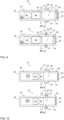
- Figures 6 to 10 schematically illustrate cross sections of detectors 10 according to a several embodiments.
- a detector 10 according to a first embodiment is shown in Figure 6 in (A) a detached state and (B) an attached state of detector body 20 and detector head 30.
- the detector body 20 comprises a plastic body part enclosing the photodetector 24 and an objective lens 42. Therein, the objective lens 42 is arranged upstream the photodetector 24 with respect to the propagation direction of incident radiation.
- the detector body 20 further comprises control electronics 29 connected at least to the photodetector 24 for controlling the photodetector 24.
- the control electronics 29 are preferably configured to communicate with a computer, e.g., via a USB connection. Also, the control electronics 29 of the detector 10 communicates with a control unit of a SEM.
- the detector body 20 further comprises a first body mounting portion 21 with a first mounting flange extending laterally from the detector body 20.
- the detector body 20 further comprises the second body mounting portion 22 also extending laterally from the detector body 20 with an extension that is less than that of the first body mounting portion 21. From the second body mounting portion, reception elements 26 protrude to form guiding grooves.
- a vacuum window 25 is disposed in between the first body mounting portion 21 and the second body mounting portion 22 with respect to the propagation direction of incident radiation.
- the detector 10 of the first embodiment further comprises a detector head 30.
- the detector head is basically formed by a hollow column 33 with a first terminal end 31 and a second terminal end 32 opposite the first terminal end 31.
- the first terminal end 31 comprises a head mounting portion 34 that is configured to be mounted to the second body mounting portion 22.
- the head mounting portion 34 comprises flange elements 37 extending laterally from the hollow column 33 with an extension that is fit to the lateral extension of the guiding grooves formed by the reception elements 26 described above.
- the detector head 30 further comprises a scintillation screen 35 disposed at the second terminal end 32 of the detector head 30 and comprising a phosphor screen configured to radiate photons in response to incident scattered electrons. These radiated photons form the incident radiation for the photodetector 24 as described above for the detector body 20.
- the detector head 30 In a detached state (A), the detector head 30 is not mounted to the detector body 20. In this state, the detector body 20 is preferably mounted to an SEM chamber port as described e.g., with respect to Figure 3 . In the attached state (B), the detector head 30 is mounted to the detector body 20 by sliding the flange elements 37 of the head mounting portion 31 in the guiding grooves of the reception elements 26 of the second body mounting portion 22.
- Figure 7 schematically illustrates a cross section of a detector 10 according to a second embodiment.
- the detector 10 of the second embodiment differs from that of the first embodiment in that a macro lens 40 is disposed adjacent the scintillation screen 35 in the propagation direction of the incident radiation, i.e., with respect to the propagation direction of the photons emitted by the scintillation screen 35 and travelling to the photodetector 24.
- Fig. 8 schematically illustrates a cross section of a detector 10 according to a third embodiment that differs from that of the second embodiment in that the macro lens 40 is arranged in the detector body 20 instead of the detector head 30. Particularly, the macro lens 40 is arranged between the vacuum window 25 and the objective lens 42 and the photodetector 24.
- Figure 9 schematically illustrates a cross section of a detector 10 according to a fourth embodiment.
- the detector 10 of the fourth embodiment differs from that of the first embodiment in that a field lens 41 is disposed adjacent the scintillation screen 35 of the detector head 30 in the propagation direction of the incident radiation, i.e., the photons emitted by the scintillation screen 35 in response to incident scattered electrons.
- the field lens 41 is configured with a high numerical aperture allowing to capture a high amount of the photons emitted by the scintillation screen 35 and to focus them on the downstream components of the detector's 10 optical system, particularly the objective lens 42.
- Figure 10 schematically illustrates a cross section of a detector 10 according to a fifth embodiment.
- the detector 10 of the fifth embodiment differs from that of the first embodiment in that the detector body 20 comprises a fiber optical taper 28 instead of the objective lens 42 and the vacuum window 25.
- the fiber optical taper 28 is formed of a plurality of optical fibers that are coherently arranged connected to form a taper with a first base surface facing the detector head and a second base surface opposite the first base surface and facing the active surface of the photodetector 24.
- the fiber optical taper 28 is configured such that an image signal input to the first base surface is transmitted as a reduced image to the second base surface. Therein, the reduction is defined by a ratio of the first and second base surface.
- the first base surface of the taper 28 is configured as vacuum window such that an additional vacuum window is omitted.
Landscapes
- Chemical & Material Sciences (AREA)
- Analytical Chemistry (AREA)
- General Physics & Mathematics (AREA)
- Physics & Mathematics (AREA)
- Health & Medical Sciences (AREA)
- Life Sciences & Earth Sciences (AREA)
- Biochemistry (AREA)
- General Health & Medical Sciences (AREA)
- Immunology (AREA)
- Pathology (AREA)
- Crystallography & Structural Chemistry (AREA)
- High Energy & Nuclear Physics (AREA)
- Molecular Biology (AREA)
- Spectroscopy & Molecular Physics (AREA)
- Measurement Of Radiation (AREA)
Claims (13)
- Detektor (10) für Kikuchi-Beugung, wobei der Detektor (10) Folgendes umfasst:einen Fotodetektor (24), der zum Detektieren einfallender Strahlung konfiguriert ist,einen Detektorkörper (20) und einen Detektorkopf (30), die aneinander montierbar sind;wobei der Detektorkörper (20) Folgendes umfasst: einen Körperteil (23), der den Fotodetektor (24) umschließt, der zum Detektieren einfallender Strahlung konfiguriert ist, ein Vakuumfenster (25), das in Bezug auf eine Ausbreitungsrichtung der einfallenden Strahlung stromaufwärts des Fotodetektors (24) angeordnet ist, und einen ersten Körpermontageabschnitt (21), der dazu konfiguriert ist, an einem Kammerport eines Rasterelektronenmikroskops (Scanning Electron Microscope - SEM) montiert zu sein, und einen zweiten Körpermontageabschnitt (22), undwobei der Detektorkopf (30) Folgendes umfasst: eine hohle Säule (33) und einen Szintillationsschirm (35), der an einem zweiten Ende (32) davon angeordnet ist, und einen Kopfmontageabschnitt (34), der mindestens ein Flanschelement (37) umfasst und dazu konfiguriert ist, über das mindestens eine Flanschelement (37), das an einem ersten Ende (31) der hohlen Säule (33) gegenüber dem zweiten Ende (32) angeordnet ist, am zweiten Körpermontageabschnitt (22) montiert zu sein,wobei der zweite Körpermontageabschnitt (22) mindestens ein Aufnahmeelement (26) umfasst, das dazu konfiguriert ist, das mindestens eine Flanschelement (37) zu führen, aufzunehmen und/oder zu befestigen.
- Detektor (10) nach Anspruch 1, wobei der erste Körpermontageabschnitt (21) zwischen dem zweiten Körpermontageabschnitt (22) und dem Fotodetektor (24) angeordnet ist.
- Detektor (10) nach Anspruch 1 oder 2, wobei der Szintillationsschirm (35) an einem Schirmhalter (36) montiert ist, der an der hohlen Säule (33) des Detektorkopfs (30) montiert ist.
- Detektor (10) nach einem der vorangehenden Ansprüche, wobei der Detektorkörper (20), insbesondere der Körperteil (23), ferner eine zwischen dem Vakuumfenster (25) und dem Fotodetektor (24) angeordnete Objektivlinse (42) umfasst.
- Detektor (10) nach einem der vorangehenden Ansprüche, wobei der Detektorkörper (20), vorzugsweise der Körperteil (23), stromaufwärts des Fotodetektors (24) in Bezug auf eine Ausbreitungsrichtung der einfallenden Strahlung einen faseroptischen Taper (28) umfasst.
- Detektor (10) nach einem der vorangehenden Ansprüche, wobei der Detektorkopf (30) ferner eine Feldlinse (41) umfasst, die in einer Ausbreitungsrichtung der einfallenden Strahlung neben dem Szintillationsschirm (35) angeordnet ist.
- Detektor (10) nach einem der vorangehenden Ansprüche, ferner umfassend eine Makrolinse (40) neben dem Vakuumfenster (25) oder neben dem Szintillationsschirm (35) in einer Ausbreitungsrichtung der einfallenden Strahlung.
- Detektorkörper (20) für den Detektorkopf (30) eines Detektors (10) nach einem der Ansprüche 1 bis 7,
wobei der Detektorkörper (20) Folgendes umfasst:einen Körperteil (20), der einen Fotodetektor (24) umschließt, der zum Detektieren einfallender Strahlung konfiguriert ist,ein Vakuumfenster (25), das in Bezug auf eine Ausbreitungsrichtung der einfallenden Strahlung stromaufwärts des Fotodetektors (25) angeordnet ist,einen ersten Körpermontageabschnitt (21), der dazu konfiguriert ist, an einem SEM-Kammerport (50) montiert zu sein, und einen zweiten Körpermontageabschnitt (22), der dazu konfiguriert ist, am Kopfmontageabschnitt (34) des Detektorkopfs (30) montiert zu sein, wobei der zweite Körpermontageabschnitt (22) mindestens ein Aufnahmeelement (26) umfasst, das dazu konfiguriert ist, das mindestens eine Flanschelement (37) zu führen, aufzunehmen und/oder zu befestigen. - Detektorkopf (30) für den Detektorkörper (20) eines Detektors (10) nach einem der Ansprüche 1 bis 7,
wobei der Detektorkopf (30) Folgendes umfasst:eine hohle Säule (33) mit einem ersten Ende (31) und einem dem ersten Ende (31) gegenüberliegenden zweiten Ende (32),einen am ersten Ende (31) angeordneten Kopfmontageabschnitt (34), der mindestens ein Flanschelement (37) umfasst und dazu konfiguriert ist, über das mindestens eine Flanschelement (37) am zweiten Körpermontageabschnitt (22) des Detektorkörpers (20) montiert zu sein, undeinen am zweiten Ende (32) montierten Szintillationsschirm (35). - Detektionssystem für Kikuchi-Beugung, umfassend:ein Rasterelektronenmikroskop (Scanning Electron Microscope - SEM) mit einer SEM-Kammer und mindestens einem SEM-Kammerport (50) zum Zugang zur SEM-Kammer; undeinen Detektor (10) nach einem der Ansprüche 1 bis 7.
- Detektionssystem nach Anspruch 10, wobei eine seitliche Erstreckung des zweiten Körpermontageabschnitts (22) kleiner als eine seitliche Erstreckung des ersten Körpermontageabschnitts (21) ist und wobei sich eine Erstreckung des zweiten Körpermontageabschnitts (22) über eine Außenwanddicke der SEM-Außenwand erstreckt, so dass der zweite Körpermontageabschnitt (22) dazu konfiguriert ist, durch den SEM-Kammerport eingeführt zu werden, bevor der erste Körpermontageabschnitt (21) an einer Außenseite des SEM-Kammerports montiert wird.
- Detektionssystem nach Anspruch 11, wobei der Körperteil (23) außerhalb der SEM-Kammer angeordnet ist und der zweite Körpermontageabschnitt (22) innerhalb der SEM-Kammer angeordnet und von innerhalb der SEM-Kammer zugänglich ist, wenn der erste Körpermontageabschnitt (21) am SEM-Kammerport (50) montiert ist, so dass der Kopfmontageabschnitt (34) von einer Innenseite einer SEM-Kammer aus am zweiten Körpermontageabschnitt (22) montierbar ist.
- Detektionssystem nach Anspruch 10, wobei die Länge der hohlen Säule (33) einem Abstand zwischen dem SEM-Kammerport (50) und einem innerhalb der SEM-Kammer montierten Probentisch oder Probenhalter entspricht.
Priority Applications (4)
| Application Number | Priority Date | Filing Date | Title |
|---|---|---|---|
| EP19188579.7A EP3770945B1 (de) | 2019-07-26 | 2019-07-26 | Detektor von kikuchi-beugung |
| JP2020124837A JP2021022563A (ja) | 2019-07-26 | 2020-07-22 | 菊池回折検出器 |
| US16/935,620 US11300530B2 (en) | 2019-07-26 | 2020-07-22 | Kikuchi diffraction detector |
| CN202010728479.6A CN112304992B (zh) | 2019-07-26 | 2020-07-24 | 菊池衍射检测器 |
Applications Claiming Priority (1)
| Application Number | Priority Date | Filing Date | Title |
|---|---|---|---|
| EP19188579.7A EP3770945B1 (de) | 2019-07-26 | 2019-07-26 | Detektor von kikuchi-beugung |
Publications (2)
| Publication Number | Publication Date |
|---|---|
| EP3770945A1 EP3770945A1 (de) | 2021-01-27 |
| EP3770945B1 true EP3770945B1 (de) | 2024-06-19 |
Family
ID=67439073
Family Applications (1)
| Application Number | Title | Priority Date | Filing Date |
|---|---|---|---|
| EP19188579.7A Active EP3770945B1 (de) | 2019-07-26 | 2019-07-26 | Detektor von kikuchi-beugung |
Country Status (4)
| Country | Link |
|---|---|
| US (1) | US11300530B2 (de) |
| EP (1) | EP3770945B1 (de) |
| JP (1) | JP2021022563A (de) |
| CN (1) | CN112304992B (de) |
Families Citing this family (5)
| Publication number | Priority date | Publication date | Assignee | Title |
|---|---|---|---|---|
| JP6914978B2 (ja) * | 2019-02-26 | 2021-08-04 | 日本電子株式会社 | 試料交換装置及び荷電粒子線装置 |
| EP3770945B1 (de) * | 2019-07-26 | 2024-06-19 | Bruker Nano GmbH | Detektor von kikuchi-beugung |
| EP3835768B1 (de) * | 2019-12-13 | 2021-10-27 | Bruker Nano GmbH | Verfahren zur verbesserung von kikuchi-beugungsmustern |
| US20220173149A1 (en) * | 2020-12-02 | 2022-06-02 | Star Tech Instruments, Inc. | Beam imaging and profiling device |
| WO2023287804A1 (en) * | 2021-07-13 | 2023-01-19 | CapeSym, Inc. | Micro-structured crystalline radiation detectors |
Family Cites Families (15)
| Publication number | Priority date | Publication date | Assignee | Title |
|---|---|---|---|---|
| US5517033A (en) * | 1994-07-25 | 1996-05-14 | Gatan, Inc. | Apparatus for improved image resolution in electron microscopy |
| CN2443366Y (zh) * | 2000-10-12 | 2001-08-15 | 北京有色金属研究总院 | 扫描电镜的接收装置 |
| GB0123053D0 (en) * | 2001-09-25 | 2001-11-14 | Oxford Instr Analytical Ltd | Electron detection device |
| GB0506907D0 (en) * | 2005-04-05 | 2005-05-11 | Oxford Instr Analytical Ltd | Method for correcting distortions in electron backscatter diffraction patterns |
| US8809783B2 (en) * | 2012-06-19 | 2014-08-19 | Rensselaer Polytechnic Institute | High spatial resolution non-contact temperature measurement |
| WO2013192608A1 (en) * | 2012-06-22 | 2013-12-27 | Edax, Inc. | Method and apparatus for electron pattern imaging |
| CN103278517B (zh) * | 2013-05-29 | 2016-03-02 | 钢铁研究总院 | 一种测量取向硅钢晶粒取向差的方法 |
| JP5464535B1 (ja) * | 2013-07-23 | 2014-04-09 | 株式会社日立ハイテクノロジーズ | Ebsd検出器で所望箇所を容易に分析できる荷電粒子線装置およびその制御方法 |
| GB201402318D0 (en) * | 2014-02-11 | 2014-03-26 | Oxford Instr Nanotechnology Tools Ltd | Method for materials analysis |
| EP3267184B1 (de) * | 2016-07-07 | 2020-03-25 | Bruker Nano GmbH | Verfahren und system zur bestimmung der position einer strahlungsquelle |
| GB2562694B (en) * | 2016-12-12 | 2020-12-30 | Vg Systems Ltd | Image capture assembly and method for electron back scatter diffraction |
| GB201715902D0 (en) * | 2017-09-29 | 2017-11-15 | Oxford Instr Plc | Improved system for electron diffraction analysis |
| EP3644341B1 (de) * | 2018-10-25 | 2025-01-22 | Bruker Nano GmbH | Beweglicher detektor |
| EP3770945B1 (de) * | 2019-07-26 | 2024-06-19 | Bruker Nano GmbH | Detektor von kikuchi-beugung |
| EP3835768B1 (de) * | 2019-12-13 | 2021-10-27 | Bruker Nano GmbH | Verfahren zur verbesserung von kikuchi-beugungsmustern |
-
2019
- 2019-07-26 EP EP19188579.7A patent/EP3770945B1/de active Active
-
2020
- 2020-07-22 JP JP2020124837A patent/JP2021022563A/ja active Pending
- 2020-07-22 US US16/935,620 patent/US11300530B2/en active Active
- 2020-07-24 CN CN202010728479.6A patent/CN112304992B/zh active Active
Also Published As
| Publication number | Publication date |
|---|---|
| EP3770945A1 (de) | 2021-01-27 |
| JP2021022563A (ja) | 2021-02-18 |
| US20210025837A1 (en) | 2021-01-28 |
| CN112304992B (zh) | 2024-03-26 |
| CN112304992A (zh) | 2021-02-02 |
| US11300530B2 (en) | 2022-04-12 |
Similar Documents
| Publication | Publication Date | Title |
|---|---|---|
| EP3770945B1 (de) | Detektor von kikuchi-beugung | |
| JP6937380B2 (ja) | X線分光を実施するための方法およびx線吸収分光システム | |
| JP5116014B2 (ja) | 小角広角x線測定装置 | |
| EP1953792B1 (de) | Vorrichtung zum Beobachten einer Probe mit einem Teilchenstrahl und einem optischen Mikroskop | |
| JP5337292B2 (ja) | 光源の変動を測定するためのシステムを備えたeuv照明システム | |
| JP5280057B2 (ja) | X線散乱用のx線回折機器 | |
| US20170052128A1 (en) | Detector for x-rays with high spatial and high spectral resolution | |
| EP3570311B1 (de) | Optischer kathodolumineszenzverteiler | |
| JP2004184314A (ja) | 蛍光x線分析装置 | |
| EP1184703B1 (de) | Mikroskop für Infrarotabbildung | |
| Hague et al. | Plane-grating flat-field soft x-ray spectrometer | |
| US20040206908A1 (en) | Primary beam stop | |
| EP3709008B1 (de) | Messsystem zur messung von eds/tkd | |
| GB2096347A (en) | Cell assembly for spectrophotometers | |
| US6596994B1 (en) | Beam position monitor | |
| Ko et al. | Development of a second generation scanning photoemission microscope with a zone plate generated microprobe at the National Synchrotron Light Source | |
| US20240047174A1 (en) | Detector and method for obtaining kikuchi images | |
| Kargl et al. | Versatile compact X-ray radiography module for materials science under microgravity conditions | |
| Bjeoumikhov et al. | New developments and applications of X‐ray capillary optics | |
| Schmidt et al. | Optical layout of a beamline for photoemission microscopy | |
| US20050069082A1 (en) | Scanning x-ray microscope with a plurality of simultaneous x-ray probes on the sample | |
| CN111272657B (zh) | 激光诱导光谱仪 | |
| JP3475097B2 (ja) | 粒径分布測定装置 | |
| JP2009505112A (ja) | X線を遮蔽するための装置及び係る装置を備えるx線装置 | |
| JP4478792B2 (ja) | 背面設置型x線検出方法 |
Legal Events
| Date | Code | Title | Description |
|---|---|---|---|
| PUAI | Public reference made under article 153(3) epc to a published international application that has entered the european phase |
Free format text: ORIGINAL CODE: 0009012 |
|
| STAA | Information on the status of an ep patent application or granted ep patent |
Free format text: STATUS: REQUEST FOR EXAMINATION WAS MADE |
|
| 17P | Request for examination filed |
Effective date: 20200612 |
|
| AK | Designated contracting states |
Kind code of ref document: A1 Designated state(s): AL AT BE BG CH CY CZ DE DK EE ES FI FR GB GR HR HU IE IS IT LI LT LU LV MC MK MT NL NO PL PT RO RS SE SI SK SM TR |
|
| AX | Request for extension of the european patent |
Extension state: BA ME |
|
| STAA | Information on the status of an ep patent application or granted ep patent |
Free format text: STATUS: EXAMINATION IS IN PROGRESS |
|
| 17Q | First examination report despatched |
Effective date: 20220530 |
|
| RIC1 | Information provided on ipc code assigned before grant |
Ipc: G01N 23/2251 20180101ALI20231123BHEP Ipc: G01N 23/203 20060101ALI20231123BHEP Ipc: G01N 23/20058 20180101ALI20231123BHEP Ipc: G01N 23/2055 20180101ALI20231123BHEP Ipc: H01J 37/256 20060101ALI20231123BHEP Ipc: H01J 37/295 20060101ALI20231123BHEP Ipc: H01J 37/28 20060101ALI20231123BHEP Ipc: H01J 37/244 20060101AFI20231123BHEP |
|
| GRAP | Despatch of communication of intention to grant a patent |
Free format text: ORIGINAL CODE: EPIDOSNIGR1 |
|
| STAA | Information on the status of an ep patent application or granted ep patent |
Free format text: STATUS: GRANT OF PATENT IS INTENDED |
|
| INTG | Intention to grant announced |
Effective date: 20240115 |
|
| GRAS | Grant fee paid |
Free format text: ORIGINAL CODE: EPIDOSNIGR3 |
|
| GRAA | (expected) grant |
Free format text: ORIGINAL CODE: 0009210 |
|
| STAA | Information on the status of an ep patent application or granted ep patent |
Free format text: STATUS: THE PATENT HAS BEEN GRANTED |
|
| AK | Designated contracting states |
Kind code of ref document: B1 Designated state(s): AL AT BE BG CH CY CZ DE DK EE ES FI FR GB GR HR HU IE IS IT LI LT LU LV MC MK MT NL NO PL PT RO RS SE SI SK SM TR |
|
| REG | Reference to a national code |
Ref country code: GB Ref legal event code: FG4D |
|
| REG | Reference to a national code |
Ref country code: CH Ref legal event code: EP |
|
| REG | Reference to a national code |
Ref country code: DE Ref legal event code: R096 Ref document number: 602019053819 Country of ref document: DE |
|
| PG25 | Lapsed in a contracting state [announced via postgrant information from national office to epo] |
Ref country code: BG Free format text: LAPSE BECAUSE OF FAILURE TO SUBMIT A TRANSLATION OF THE DESCRIPTION OR TO PAY THE FEE WITHIN THE PRESCRIBED TIME-LIMIT Effective date: 20240619 |
|
| PG25 | Lapsed in a contracting state [announced via postgrant information from national office to epo] |
Ref country code: FI Free format text: LAPSE BECAUSE OF FAILURE TO SUBMIT A TRANSLATION OF THE DESCRIPTION OR TO PAY THE FEE WITHIN THE PRESCRIBED TIME-LIMIT Effective date: 20240619 Ref country code: HR Free format text: LAPSE BECAUSE OF FAILURE TO SUBMIT A TRANSLATION OF THE DESCRIPTION OR TO PAY THE FEE WITHIN THE PRESCRIBED TIME-LIMIT Effective date: 20240619 |
|
| REG | Reference to a national code |
Ref country code: LT Ref legal event code: MG9D |
|
| PG25 | Lapsed in a contracting state [announced via postgrant information from national office to epo] |
Ref country code: GR Free format text: LAPSE BECAUSE OF FAILURE TO SUBMIT A TRANSLATION OF THE DESCRIPTION OR TO PAY THE FEE WITHIN THE PRESCRIBED TIME-LIMIT Effective date: 20240920 |
|
| REG | Reference to a national code |
Ref country code: NL Ref legal event code: MP Effective date: 20240619 |
|
| PG25 | Lapsed in a contracting state [announced via postgrant information from national office to epo] |
Ref country code: LV Free format text: LAPSE BECAUSE OF FAILURE TO SUBMIT A TRANSLATION OF THE DESCRIPTION OR TO PAY THE FEE WITHIN THE PRESCRIBED TIME-LIMIT Effective date: 20240619 |
|
| PG25 | Lapsed in a contracting state [announced via postgrant information from national office to epo] |
Ref country code: NO Free format text: LAPSE BECAUSE OF FAILURE TO SUBMIT A TRANSLATION OF THE DESCRIPTION OR TO PAY THE FEE WITHIN THE PRESCRIBED TIME-LIMIT Effective date: 20240919 Ref country code: LV Free format text: LAPSE BECAUSE OF FAILURE TO SUBMIT A TRANSLATION OF THE DESCRIPTION OR TO PAY THE FEE WITHIN THE PRESCRIBED TIME-LIMIT Effective date: 20240619 Ref country code: HR Free format text: LAPSE BECAUSE OF FAILURE TO SUBMIT A TRANSLATION OF THE DESCRIPTION OR TO PAY THE FEE WITHIN THE PRESCRIBED TIME-LIMIT Effective date: 20240619 Ref country code: GR Free format text: LAPSE BECAUSE OF FAILURE TO SUBMIT A TRANSLATION OF THE DESCRIPTION OR TO PAY THE FEE WITHIN THE PRESCRIBED TIME-LIMIT Effective date: 20240920 Ref country code: FI Free format text: LAPSE BECAUSE OF FAILURE TO SUBMIT A TRANSLATION OF THE DESCRIPTION OR TO PAY THE FEE WITHIN THE PRESCRIBED TIME-LIMIT Effective date: 20240619 Ref country code: BG Free format text: LAPSE BECAUSE OF FAILURE TO SUBMIT A TRANSLATION OF THE DESCRIPTION OR TO PAY THE FEE WITHIN THE PRESCRIBED TIME-LIMIT Effective date: 20240619 Ref country code: RS Free format text: LAPSE BECAUSE OF FAILURE TO SUBMIT A TRANSLATION OF THE DESCRIPTION OR TO PAY THE FEE WITHIN THE PRESCRIBED TIME-LIMIT Effective date: 20240919 |
|
| PG25 | Lapsed in a contracting state [announced via postgrant information from national office to epo] |
Ref country code: NL Free format text: LAPSE BECAUSE OF FAILURE TO SUBMIT A TRANSLATION OF THE DESCRIPTION OR TO PAY THE FEE WITHIN THE PRESCRIBED TIME-LIMIT Effective date: 20240619 |
|
| REG | Reference to a national code |
Ref country code: AT Ref legal event code: MK05 Ref document number: 1696505 Country of ref document: AT Kind code of ref document: T Effective date: 20240619 |
|
| PG25 | Lapsed in a contracting state [announced via postgrant information from national office to epo] |
Ref country code: NL Free format text: LAPSE BECAUSE OF FAILURE TO SUBMIT A TRANSLATION OF THE DESCRIPTION OR TO PAY THE FEE WITHIN THE PRESCRIBED TIME-LIMIT Effective date: 20240619 |
|
| PG25 | Lapsed in a contracting state [announced via postgrant information from national office to epo] |
Ref country code: PT Free format text: LAPSE BECAUSE OF FAILURE TO SUBMIT A TRANSLATION OF THE DESCRIPTION OR TO PAY THE FEE WITHIN THE PRESCRIBED TIME-LIMIT Effective date: 20241021 |
|
| PG25 | Lapsed in a contracting state [announced via postgrant information from national office to epo] |
Ref country code: PT Free format text: LAPSE BECAUSE OF FAILURE TO SUBMIT A TRANSLATION OF THE DESCRIPTION OR TO PAY THE FEE WITHIN THE PRESCRIBED TIME-LIMIT Effective date: 20241021 |
|
| PG25 | Lapsed in a contracting state [announced via postgrant information from national office to epo] |
Ref country code: PL Free format text: LAPSE BECAUSE OF FAILURE TO SUBMIT A TRANSLATION OF THE DESCRIPTION OR TO PAY THE FEE WITHIN THE PRESCRIBED TIME-LIMIT Effective date: 20240619 |
|
| PG25 | Lapsed in a contracting state [announced via postgrant information from national office to epo] |
Ref country code: EE Free format text: LAPSE BECAUSE OF FAILURE TO SUBMIT A TRANSLATION OF THE DESCRIPTION OR TO PAY THE FEE WITHIN THE PRESCRIBED TIME-LIMIT Effective date: 20240619 |
|
| PG25 | Lapsed in a contracting state [announced via postgrant information from national office to epo] |
Ref country code: IS Free format text: LAPSE BECAUSE OF FAILURE TO SUBMIT A TRANSLATION OF THE DESCRIPTION OR TO PAY THE FEE WITHIN THE PRESCRIBED TIME-LIMIT Effective date: 20241019 Ref country code: AT Free format text: LAPSE BECAUSE OF FAILURE TO SUBMIT A TRANSLATION OF THE DESCRIPTION OR TO PAY THE FEE WITHIN THE PRESCRIBED TIME-LIMIT Effective date: 20240619 |
|
| PG25 | Lapsed in a contracting state [announced via postgrant information from national office to epo] |
Ref country code: CZ Free format text: LAPSE BECAUSE OF FAILURE TO SUBMIT A TRANSLATION OF THE DESCRIPTION OR TO PAY THE FEE WITHIN THE PRESCRIBED TIME-LIMIT Effective date: 20240619 |
|
| PG25 | Lapsed in a contracting state [announced via postgrant information from national office to epo] |
Ref country code: SK Free format text: LAPSE BECAUSE OF FAILURE TO SUBMIT A TRANSLATION OF THE DESCRIPTION OR TO PAY THE FEE WITHIN THE PRESCRIBED TIME-LIMIT Effective date: 20240619 Ref country code: RO Free format text: LAPSE BECAUSE OF FAILURE TO SUBMIT A TRANSLATION OF THE DESCRIPTION OR TO PAY THE FEE WITHIN THE PRESCRIBED TIME-LIMIT Effective date: 20240619 |
|
| PG25 | Lapsed in a contracting state [announced via postgrant information from national office to epo] |
Ref country code: SM Free format text: LAPSE BECAUSE OF FAILURE TO SUBMIT A TRANSLATION OF THE DESCRIPTION OR TO PAY THE FEE WITHIN THE PRESCRIBED TIME-LIMIT Effective date: 20240619 Ref country code: ES Free format text: LAPSE BECAUSE OF FAILURE TO SUBMIT A TRANSLATION OF THE DESCRIPTION OR TO PAY THE FEE WITHIN THE PRESCRIBED TIME-LIMIT Effective date: 20240619 |
|
| PG25 | Lapsed in a contracting state [announced via postgrant information from national office to epo] |
Ref country code: SM Free format text: LAPSE BECAUSE OF FAILURE TO SUBMIT A TRANSLATION OF THE DESCRIPTION OR TO PAY THE FEE WITHIN THE PRESCRIBED TIME-LIMIT Effective date: 20240619 Ref country code: SK Free format text: LAPSE BECAUSE OF FAILURE TO SUBMIT A TRANSLATION OF THE DESCRIPTION OR TO PAY THE FEE WITHIN THE PRESCRIBED TIME-LIMIT Effective date: 20240619 Ref country code: RO Free format text: LAPSE BECAUSE OF FAILURE TO SUBMIT A TRANSLATION OF THE DESCRIPTION OR TO PAY THE FEE WITHIN THE PRESCRIBED TIME-LIMIT Effective date: 20240619 Ref country code: PL Free format text: LAPSE BECAUSE OF FAILURE TO SUBMIT A TRANSLATION OF THE DESCRIPTION OR TO PAY THE FEE WITHIN THE PRESCRIBED TIME-LIMIT Effective date: 20240619 Ref country code: IS Free format text: LAPSE BECAUSE OF FAILURE TO SUBMIT A TRANSLATION OF THE DESCRIPTION OR TO PAY THE FEE WITHIN THE PRESCRIBED TIME-LIMIT Effective date: 20241019 Ref country code: ES Free format text: LAPSE BECAUSE OF FAILURE TO SUBMIT A TRANSLATION OF THE DESCRIPTION OR TO PAY THE FEE WITHIN THE PRESCRIBED TIME-LIMIT Effective date: 20240619 Ref country code: EE Free format text: LAPSE BECAUSE OF FAILURE TO SUBMIT A TRANSLATION OF THE DESCRIPTION OR TO PAY THE FEE WITHIN THE PRESCRIBED TIME-LIMIT Effective date: 20240619 Ref country code: CZ Free format text: LAPSE BECAUSE OF FAILURE TO SUBMIT A TRANSLATION OF THE DESCRIPTION OR TO PAY THE FEE WITHIN THE PRESCRIBED TIME-LIMIT Effective date: 20240619 Ref country code: AT Free format text: LAPSE BECAUSE OF FAILURE TO SUBMIT A TRANSLATION OF THE DESCRIPTION OR TO PAY THE FEE WITHIN THE PRESCRIBED TIME-LIMIT Effective date: 20240619 |
|
| PG25 | Lapsed in a contracting state [announced via postgrant information from national office to epo] |
Ref country code: IT Free format text: LAPSE BECAUSE OF FAILURE TO SUBMIT A TRANSLATION OF THE DESCRIPTION OR TO PAY THE FEE WITHIN THE PRESCRIBED TIME-LIMIT Effective date: 20240619 |
|
| REG | Reference to a national code |
Ref country code: CH Ref legal event code: PL |
|
| PG25 | Lapsed in a contracting state [announced via postgrant information from national office to epo] |
Ref country code: LU Free format text: LAPSE BECAUSE OF NON-PAYMENT OF DUE FEES Effective date: 20240726 |
|
| PG25 | Lapsed in a contracting state [announced via postgrant information from national office to epo] |
Ref country code: MC Free format text: LAPSE BECAUSE OF FAILURE TO SUBMIT A TRANSLATION OF THE DESCRIPTION OR TO PAY THE FEE WITHIN THE PRESCRIBED TIME-LIMIT Effective date: 20240619 |
|
| REG | Reference to a national code |
Ref country code: DE Ref legal event code: R097 Ref document number: 602019053819 Country of ref document: DE |
|
| PG25 | Lapsed in a contracting state [announced via postgrant information from national office to epo] |
Ref country code: MC Free format text: LAPSE BECAUSE OF FAILURE TO SUBMIT A TRANSLATION OF THE DESCRIPTION OR TO PAY THE FEE WITHIN THE PRESCRIBED TIME-LIMIT Effective date: 20240619 Ref country code: LU Free format text: LAPSE BECAUSE OF NON-PAYMENT OF DUE FEES Effective date: 20240726 |
|
| PG25 | Lapsed in a contracting state [announced via postgrant information from national office to epo] |
Ref country code: DK Free format text: LAPSE BECAUSE OF FAILURE TO SUBMIT A TRANSLATION OF THE DESCRIPTION OR TO PAY THE FEE WITHIN THE PRESCRIBED TIME-LIMIT Effective date: 20240619 |
|
| PG25 | Lapsed in a contracting state [announced via postgrant information from national office to epo] |
Ref country code: BE Free format text: LAPSE BECAUSE OF NON-PAYMENT OF DUE FEES Effective date: 20240731 Ref country code: CH Free format text: LAPSE BECAUSE OF NON-PAYMENT OF DUE FEES Effective date: 20240731 |
|
| PLBE | No opposition filed within time limit |
Free format text: ORIGINAL CODE: 0009261 |
|
| STAA | Information on the status of an ep patent application or granted ep patent |
Free format text: STATUS: NO OPPOSITION FILED WITHIN TIME LIMIT |
|
| 26N | No opposition filed |
Effective date: 20250320 |
|
| GBPC | Gb: european patent ceased through non-payment of renewal fee |
Effective date: 20240919 |
|
| REG | Reference to a national code |
Ref country code: BE Ref legal event code: MM Effective date: 20240731 |
|
| PG25 | Lapsed in a contracting state [announced via postgrant information from national office to epo] |
Ref country code: GB Free format text: LAPSE BECAUSE OF NON-PAYMENT OF DUE FEES Effective date: 20240919 |
|
| PG25 | Lapsed in a contracting state [announced via postgrant information from national office to epo] |
Ref country code: FR Free format text: LAPSE BECAUSE OF NON-PAYMENT OF DUE FEES Effective date: 20240819 |
|
| PG25 | Lapsed in a contracting state [announced via postgrant information from national office to epo] |
Ref country code: IE Free format text: LAPSE BECAUSE OF NON-PAYMENT OF DUE FEES Effective date: 20240726 |
|
| PG25 | Lapsed in a contracting state [announced via postgrant information from national office to epo] |
Ref country code: SE Free format text: LAPSE BECAUSE OF FAILURE TO SUBMIT A TRANSLATION OF THE DESCRIPTION OR TO PAY THE FEE WITHIN THE PRESCRIBED TIME-LIMIT Effective date: 20240619 |
|
| PGFP | Annual fee paid to national office [announced via postgrant information from national office to epo] |
Ref country code: DE Payment date: 20250626 Year of fee payment: 7 |
|
| PG25 | Lapsed in a contracting state [announced via postgrant information from national office to epo] |
Ref country code: CY Free format text: LAPSE BECAUSE OF FAILURE TO SUBMIT A TRANSLATION OF THE DESCRIPTION OR TO PAY THE FEE WITHIN THE PRESCRIBED TIME-LIMIT; INVALID AB INITIO Effective date: 20190726 |
|
| PG25 | Lapsed in a contracting state [announced via postgrant information from national office to epo] |
Ref country code: HU Free format text: LAPSE BECAUSE OF FAILURE TO SUBMIT A TRANSLATION OF THE DESCRIPTION OR TO PAY THE FEE WITHIN THE PRESCRIBED TIME-LIMIT; INVALID AB INITIO Effective date: 20190726 |