EP3764487A1 - Light emitting element mounting substrate and light emitting device - Google Patents
Light emitting element mounting substrate and light emitting device Download PDFInfo
- Publication number
- EP3764487A1 EP3764487A1 EP19763419.9A EP19763419A EP3764487A1 EP 3764487 A1 EP3764487 A1 EP 3764487A1 EP 19763419 A EP19763419 A EP 19763419A EP 3764487 A1 EP3764487 A1 EP 3764487A1
- Authority
- EP
- European Patent Office
- Prior art keywords
- conductor
- substrate
- light
- emitting element
- via conductor
- Prior art date
- Legal status (The legal status is an assumption and is not a legal conclusion. Google has not performed a legal analysis and makes no representation as to the accuracy of the status listed.)
- Withdrawn
Links
Images





Classifications
-
- H—ELECTRICITY
- H01—ELECTRIC ELEMENTS
- H01S—DEVICES USING THE PROCESS OF LIGHT AMPLIFICATION BY STIMULATED EMISSION OF RADIATION [LASER] TO AMPLIFY OR GENERATE LIGHT; DEVICES USING STIMULATED EMISSION OF ELECTROMAGNETIC RADIATION IN WAVE RANGES OTHER THAN OPTICAL
- H01S5/00—Semiconductor lasers
- H01S5/02—Structural details or components not essential to laser action
- H01S5/022—Mountings; Housings
- H01S5/023—Mount members, e.g. sub-mount members
-
- H—ELECTRICITY
- H05—ELECTRIC TECHNIQUES NOT OTHERWISE PROVIDED FOR
- H05K—PRINTED CIRCUITS; CASINGS OR CONSTRUCTIONAL DETAILS OF ELECTRIC APPARATUS; MANUFACTURE OF ASSEMBLAGES OF ELECTRICAL COMPONENTS
- H05K1/00—Printed circuits
- H05K1/02—Details
- H05K1/0213—Electrical arrangements not otherwise provided for
- H05K1/0263—High current adaptations, e.g. printed high current conductors or using auxiliary non-printed means; Fine and coarse circuit patterns on one circuit board
- H05K1/0265—High current adaptations, e.g. printed high current conductors or using auxiliary non-printed means; Fine and coarse circuit patterns on one circuit board characterized by the lay-out of or details of the printed conductors, e.g. reinforced conductors, redundant conductors, conductors having different cross-sections
-
- H—ELECTRICITY
- H01—ELECTRIC ELEMENTS
- H01S—DEVICES USING THE PROCESS OF LIGHT AMPLIFICATION BY STIMULATED EMISSION OF RADIATION [LASER] TO AMPLIFY OR GENERATE LIGHT; DEVICES USING STIMULATED EMISSION OF ELECTROMAGNETIC RADIATION IN WAVE RANGES OTHER THAN OPTICAL
- H01S5/00—Semiconductor lasers
- H01S5/02—Structural details or components not essential to laser action
- H01S5/022—Mountings; Housings
-
- H—ELECTRICITY
- H01—ELECTRIC ELEMENTS
- H01S—DEVICES USING THE PROCESS OF LIGHT AMPLIFICATION BY STIMULATED EMISSION OF RADIATION [LASER] TO AMPLIFY OR GENERATE LIGHT; DEVICES USING STIMULATED EMISSION OF ELECTROMAGNETIC RADIATION IN WAVE RANGES OTHER THAN OPTICAL
- H01S5/00—Semiconductor lasers
- H01S5/02—Structural details or components not essential to laser action
- H01S5/022—Mountings; Housings
- H01S5/0233—Mounting configuration of laser chips
-
- H—ELECTRICITY
- H01—ELECTRIC ELEMENTS
- H01S—DEVICES USING THE PROCESS OF LIGHT AMPLIFICATION BY STIMULATED EMISSION OF RADIATION [LASER] TO AMPLIFY OR GENERATE LIGHT; DEVICES USING STIMULATED EMISSION OF ELECTROMAGNETIC RADIATION IN WAVE RANGES OTHER THAN OPTICAL
- H01S5/00—Semiconductor lasers
- H01S5/02—Structural details or components not essential to laser action
- H01S5/022—Mountings; Housings
- H01S5/0235—Method for mounting laser chips
-
- H—ELECTRICITY
- H01—ELECTRIC ELEMENTS
- H01S—DEVICES USING THE PROCESS OF LIGHT AMPLIFICATION BY STIMULATED EMISSION OF RADIATION [LASER] TO AMPLIFY OR GENERATE LIGHT; DEVICES USING STIMULATED EMISSION OF ELECTROMAGNETIC RADIATION IN WAVE RANGES OTHER THAN OPTICAL
- H01S5/00—Semiconductor lasers
- H01S5/02—Structural details or components not essential to laser action
- H01S5/022—Mountings; Housings
- H01S5/0235—Method for mounting laser chips
- H01S5/02355—Fixing laser chips on mounts
- H01S5/0237—Fixing laser chips on mounts by soldering
-
- H—ELECTRICITY
- H01—ELECTRIC ELEMENTS
- H01S—DEVICES USING THE PROCESS OF LIGHT AMPLIFICATION BY STIMULATED EMISSION OF RADIATION [LASER] TO AMPLIFY OR GENERATE LIGHT; DEVICES USING STIMULATED EMISSION OF ELECTROMAGNETIC RADIATION IN WAVE RANGES OTHER THAN OPTICAL
- H01S5/00—Semiconductor lasers
- H01S5/02—Structural details or components not essential to laser action
- H01S5/022—Mountings; Housings
- H01S5/0239—Combinations of electrical or optical elements
-
- H—ELECTRICITY
- H05—ELECTRIC TECHNIQUES NOT OTHERWISE PROVIDED FOR
- H05K—PRINTED CIRCUITS; CASINGS OR CONSTRUCTIONAL DETAILS OF ELECTRIC APPARATUS; MANUFACTURE OF ASSEMBLAGES OF ELECTRICAL COMPONENTS
- H05K1/00—Printed circuits
- H05K1/02—Details
- H05K1/03—Use of materials for the substrate
- H05K1/0306—Inorganic insulating substrates, e.g. ceramic, glass
-
- H—ELECTRICITY
- H05—ELECTRIC TECHNIQUES NOT OTHERWISE PROVIDED FOR
- H05K—PRINTED CIRCUITS; CASINGS OR CONSTRUCTIONAL DETAILS OF ELECTRIC APPARATUS; MANUFACTURE OF ASSEMBLAGES OF ELECTRICAL COMPONENTS
- H05K1/00—Printed circuits
- H05K1/02—Details
- H05K1/11—Printed elements for providing electric connections to or between printed circuits
- H05K1/111—Pads for surface mounting, e.g. lay-out
- H05K1/112—Pads for surface mounting, e.g. lay-out directly combined with via connections
- H05K1/113—Via provided in pad; Pad over filled via
-
- H—ELECTRICITY
- H05—ELECTRIC TECHNIQUES NOT OTHERWISE PROVIDED FOR
- H05K—PRINTED CIRCUITS; CASINGS OR CONSTRUCTIONAL DETAILS OF ELECTRIC APPARATUS; MANUFACTURE OF ASSEMBLAGES OF ELECTRICAL COMPONENTS
- H05K2201/00—Indexing scheme relating to printed circuits covered by H05K1/00
- H05K2201/09—Shape and layout
- H05K2201/09209—Shape and layout details of conductors
- H05K2201/095—Conductive through-holes or vias
- H05K2201/09627—Special connections between adjacent vias, not for grounding vias
-
- H—ELECTRICITY
- H05—ELECTRIC TECHNIQUES NOT OTHERWISE PROVIDED FOR
- H05K—PRINTED CIRCUITS; CASINGS OR CONSTRUCTIONAL DETAILS OF ELECTRIC APPARATUS; MANUFACTURE OF ASSEMBLAGES OF ELECTRICAL COMPONENTS
- H05K2201/00—Indexing scheme relating to printed circuits covered by H05K1/00
- H05K2201/09—Shape and layout
- H05K2201/09209—Shape and layout details of conductors
- H05K2201/09654—Shape and layout details of conductors covering at least two types of conductors provided for in H05K2201/09218 - H05K2201/095
- H05K2201/0979—Redundant conductors or connections, i.e. more than one current path between two points
-
- H—ELECTRICITY
- H05—ELECTRIC TECHNIQUES NOT OTHERWISE PROVIDED FOR
- H05K—PRINTED CIRCUITS; CASINGS OR CONSTRUCTIONAL DETAILS OF ELECTRIC APPARATUS; MANUFACTURE OF ASSEMBLAGES OF ELECTRICAL COMPONENTS
- H05K2201/00—Indexing scheme relating to printed circuits covered by H05K1/00
- H05K2201/10—Details of components or other objects attached to or integrated in a printed circuit board
- H05K2201/10007—Types of components
- H05K2201/10106—Light emitting diode [LED]
-
- H—ELECTRICITY
- H05—ELECTRIC TECHNIQUES NOT OTHERWISE PROVIDED FOR
- H05K—PRINTED CIRCUITS; CASINGS OR CONSTRUCTIONAL DETAILS OF ELECTRIC APPARATUS; MANUFACTURE OF ASSEMBLAGES OF ELECTRICAL COMPONENTS
- H05K3/00—Apparatus or processes for manufacturing printed circuits
- H05K3/46—Manufacturing multilayer circuits
- H05K3/4611—Manufacturing multilayer circuits by laminating two or more circuit boards
- H05K3/4626—Manufacturing multilayer circuits by laminating two or more circuit boards characterised by the insulating layers or materials
- H05K3/4629—Manufacturing multilayer circuits by laminating two or more circuit boards characterised by the insulating layers or materials laminating inorganic sheets comprising printed circuits, e.g. green ceramic sheets
-
- H—ELECTRICITY
- H10—SEMICONDUCTOR DEVICES; ELECTRIC SOLID-STATE DEVICES NOT OTHERWISE PROVIDED FOR
- H10H—INORGANIC LIGHT-EMITTING SEMICONDUCTOR DEVICES HAVING POTENTIAL BARRIERS
- H10H20/00—Individual inorganic light-emitting semiconductor devices having potential barriers, e.g. light-emitting diodes [LED]
- H10H20/80—Constructional details
- H10H20/85—Packages
- H10H20/8506—Containers
-
- H—ELECTRICITY
- H10—SEMICONDUCTOR DEVICES; ELECTRIC SOLID-STATE DEVICES NOT OTHERWISE PROVIDED FOR
- H10H—INORGANIC LIGHT-EMITTING SEMICONDUCTOR DEVICES HAVING POTENTIAL BARRIERS
- H10H20/00—Individual inorganic light-emitting semiconductor devices having potential barriers, e.g. light-emitting diodes [LED]
- H10H20/80—Constructional details
- H10H20/85—Packages
- H10H20/857—Interconnections, e.g. lead-frames, bond wires or solder balls
Definitions
- Disclosed embodiments relate to a substrate for mounting a light-emitting element and a light-emitting device.
- a substrate that has a light-emitting element connection terminal pad and an external connection terminal pad that are formed on an insulated substrate and a conductor wiring that is formed on the insulated substrate and is electrically connected between both such pads has conventionally been known as a substrate for mounting a light-emitting element to mount a light-emitting element (see, for example, Patent Literature 1).
- Patent Literature 1 Japanese Patent Application Publication No. 2010-199167
- a substrate for mounting a light-emitting element includes a substrate that is composed of a ceramic(s), a terminal for an element that is provided on a front surface of the substrate where a light-emitting element is mounted thereon, a terminal for a power source that is provided on the substrate where an external power source is connected thereto, and a wiring part that is provided inside the substrate and electrically connects the terminal for an element and the terminal for a power source. Furthermore, the wiring part has a first conductor that extends in a surface direction of the substrate, and a second conductor that extends in substantially parallel to the first conductor on an opposite side of the front surface and is connected in parallel with the first conductor.
- a light-emitting device includes the substrate for mounting a light-emitting element as described above, and a light-emitting element that is mounted on the terminal for an element of the substrate for mounting a light-emitting element.
- a substrate for mounting a light-emitting element and a light-emitting device as disclosed in the present application will be explained with reference to the accompanying drawings. Additionally, this invention is not limited to a substrate for mounting a light-emitting element or a light-emitting device, and it goes without saying that it is possible to apply it to a substrate or device that mounts a general electrical element that has a heat generation property, other than a light-emitting element.
- LSI Large Scale Integrated circuit
- CCD Charge Coupled Device
- Laser Diode Laser Diode
- LED Light Emitting Diode
- a substrate for mounting a light-emitting element A1 includes a substrate 10 with a flat plate shape that is composed of a ceramic(s). Furthermore, terminals for an element 11a, 11b that are composed of a metal are provided on a front surface 10a of such a substrate 10. Furthermore, terminals for a power source 12a, 12b are provided on the substrate 10. Additionally, in such a case, although FIG.
- FIG. 1A illustrates a structure where the terminals for an element 11a, 11b and the terminals for a power source 12a, 12b are provided on the front surface 10a of the substrate 10, the front surface 10a of the substrate 10 is not limiting and the terminals for a power source 12a, 12b may be provided on an end surface 10c or a side surface 10d of the substrate 10.
- the terminal for an element 11a is a terminal where a light-emitting element 30 is mounted thereon.
- the terminal for an element 11b is a terminal where the light-emitting element 30 that is mounted on the terminal for an element 11a is connected thereto by a bonding wire or the like.
- the terminals for a power source 12a, 12b are terminals where a non-illustrated external power source is connected thereto.
- the terminal for an element 11a and the terminal for a power source 12a are electrically connected through a wiring part 14a and the terminal for an element 11b and the terminal for a power source 12b are electrically connected through a wiring part 14b.
- the wiring part 14a is formed inside the substrate 10 and has a first conductor 15a, a second conductor 16a, a first via conductor 17a, a second via conductor 18a, a third via conductor 19a, and a fourth via conductor 20a.
- the wiring part 14b is also formed inside the substrate 10 and has a first conductor 15b, a second conductor 16b, a first via conductor 17b, a second via conductor 18b, a third via conductor 19b, and a fourth via conductor 20b.
- the wiring part 14b has a configuration similar to that of the wiring part 14a, so that a configuration of the wiring part 14a will be explained in the following explanation and an explanation of the wiring part 14b will be omitted therein.
- any of the first conductor 15a and the second conductor 16a is composed of a metal and extends in a surface direction of the substrate 10 (that is, substantially parallel to the front surface 10a of the substrate 10).
- the first conductor 15a and the second conductor 16a extend so as to be along the front surface 10a of the substrate 10.
- any of the first conductor 15a and the second conductor 16a extends in such a manner that one end side thereof reaches a lower side of the terminal for an element 11a, and extends in such a manner that another end side thereof reaches a lower side of the terminal for a power source 12a.
- first conductor 15a and the second conductor 16a are arranged side by side inside the substrate 10 in a thickness direction thereof (that is, substantially perpendicular to the front surface 10a of the substrate 10).
- “being composed of a metal” means that, for example, a ceramic(s) other than a metal may be included partially. A similar meaning also applies below.
- the second conductor 16a is arranged on an opposite side of the front surface 10a with respect to the first conductor 15a. That is, the second conductor 16a is arranged so as to be more distant from the front surface 10a than the first conductor 15a.
- any of the first via conductor 17a to the fourth via conductor 20a is composed of a metal and extends in a thickness direction of the substrate 10.
- the first via conductor 17a is arranged on a lower side of the terminal for an element 11a and is connected between such a terminal for an element 11a and the first conductor 15a.
- the second via conductor 18a is arranged on a lower side of the terminal for a power source 12a and is connected between such a terminal for a power source 12a and the first conductor 15a.
- the third via conductor 19a is arranged on a lower side of the terminal for an element 11a and is connected between the first conductor 15a and the second conductor 16a.
- the fourth via conductor 20a is arranged on a lower side of the terminal for a power source 12a and is connected between the first conductor 15a and the second conductor 16a.
- the wiring part 14a has a wiring that sequentially wire-connects the first via conductor 17a, the first conductor 15a, and the second via conductor 18a and a wiring that sequentially wire-connects the first via conductor 17a, the first conductor 15a, the third via conductor 19a, the second conductor 16a, the fourth via conductor 20a, the first conductor 15a, and the second via conductor 18a. That is, the wiring part 14a where wirings are formed in parallel is connected between the terminal for an element 11a and the terminal for a power source 12a.
- the wiring part 14a is a wiring that is a single wire. Therefore, according to an embodiment, it is possible to maintain a pulse waveform in a state that is close to a rectangular shape when the light-emitting element 30 is pulse-driven by an external power source that is connected to the terminals for a power source 12a, 12b, so that it is possible to prevent or reduce a variation in an output of light emission in the light-emitting element 30.
- the first conductor 15a and the second conductor 16a are arranged in such a manner that both parts with a less thickness face one another in upward and downward directions. Thereby, it is possible to provide the first conductor 15a and the second conductor 16a closely in a thickness direction of the substrate 10. Therefore, according to an embodiment, it is possible to further reduce a wiring resistance of the wiring part 14a.
- a ceramic site of the substrate 10 is present between the first conductor 15a and the second conductor 16a. If the first conductor 15a and the second conductor 16a are integrated and the wiring part 14a is composed of a thick conductor that extends in a surface direction, there is a great difference in a coefficient of thermal expansion between a thick conductor of a metal and the substrate 10 of a ceramic(s), so that a great stress may be generated between the thick conductor and the substrate 10. Therefore, in such a case, a reliability of the substrate for mounting a light-emitting element A1 may be degraded.
- a site of the wiring part 14a that extends in a surface direction is divided into the first conductor 15a and the second conductor 16a and a ceramic site is present therebetween, so that it is possible to reduce a stress that is generated between a set of the first conductor 15a and the second conductor 16a and the substrate 10. Therefore, according to an embodiment, it is possible to improve a reliability of the substrate for mounting a light-emitting element A1.
- the second conductor 16a with a high thermal conductivity at a position that is close to a back surface 10b of the substrate 10.
- the back surface 10b is a surface of the substrate 10 on an opposite side of the front surface 10a.
- the first via conductor 17a and the third via conductor 19a are arranged at substantially identical positions, and the second via conductor 18a and the fourth via conductor 20a are arranged at substantially identical positions.
- the first via conductor 17a and the third via conductor 19a being arranged at substantially identical positions refers to a state where a site that overlaps in a thickness direction of the substrate 10 is present between the first via conductor 17a and the third via conductor 19a.
- a similar matter is also applied between the second via conductor 18a and the fourth via conductor 20a.
- lengths of the first conductor 15a and the second conductor 16a are substantially equal.
- a length between the first conductor 15a and the second conductor 16a being substantially equal refers to a case where a difference in a length between the first conductor 15a and the second conductor 16a is less than or equal to a diameters of via conductors that are provided on both ends of such a first conductor 15a and a second conductor 16a.
- a diameter of a via conductor is a minimum diameter among diameters of the first via conductor 17a, the second via conductor 18a, the third via conductor 19a, and the fourth via conductor 20a.
- a via conductor other than the third via conductor 19a and the fourth via conductor 20a may be connected between the first conductor 15a and the second conductor 16a.
- a fifth via conductor 21a may be connected between a middle part of the first conductor 15a and a middle part of the second conductor 16a.
- a fifth via conductor 21b may be connected between a middle part of the first conductor 15b and a middle part of the second conductor 16b. Thereby, it is possible to further equalize a current that flows through the first conductor 15b and a current that flows through the second conductor 16b.
- any of the first conductor 15a and the second conductor 16a is arranged to be substantially parallel to the front surface 10a. Thereby, it is possible to arrange the first conductor 15a and the second conductor 16a more closely.
- the substrate 10 is formed of a ceramic(s).
- a ceramic(s) for example, alumina, silica, mullite, cordierite, forsterite, aluminum nitride, silicon nitride, silicon carbide, a glass ceramic(s), or the like is suitable.
- the substrate 10 includes aluminum nitride (AlN) as a main component, from the viewpoint of a high thermal conductivity and a coefficient of thermal expansion that is close to that of the light-emitting element 30.
- the substrate 10 including aluminum nitride as a main component refers to the substrate 10 including 80% by mass or more of aluminum nitride. In a case where 80% by mass or more of aluminum nitride is included in the substrate 10, a thermal conductivity of the substrate for mounting a light-emitting element A1 is increased, so that it is possible to improve a heat release property thereof.
- the substrate 10 includes 90% by mass or more of aluminum nitride.
- a content of aluminum nitride is 90% by mass or more, it is possible for a thermal conductivity of the substrate 10 to be 150 W/mK or greater, so that it is possible to realize the substrate for mounting a light-emitting element A1 with an excellent heat release property.
- the terminals for an element 11a, 11b are formed of a metallized film where a metal powder is sintered. It is possible to bond a metallized film to a ceramic surface that composes the substrate 10, with a high strength, so that it is possible to realize the substrate for mounting a light-emitting element A1 with a high reliability.
- a plating film of Ni or the like may be formed on a surface of such a metallized film.
- a solder or an Au-Sn plating film may be provided on a surface of such a plating film.
- a metal film for sealing 13 is provided on the front surface 10a of the substrate 10 so as to surround the terminals for an element 11a, 11b.
- the metal film for sealing 13 is a site where, when a cap 40 is provided so as to cover the light-emitting element 30 that is mounted on the terminal for an element 11a, such a cap 40 is bonded thereto.
- the terminals for a power source 12a, 12b are also metallized films similarly to the terminals for an element 11a, 11b, and further, a plating film may also be formed on the terminals for a power source 12a, 12b.
- the first via conductor 17a to the fourth via conductor 20a are also metallized films where a metal powder is fired.
- a light-emitting device is configured in such a manner that the light-emitting element 30 and the cap 40 are mounted on the substrate for mounting a light-emitting element A1 as explained thus far.
- the light-emitting element 30 it is possible to use, for example, a semiconductor laser (that is also referred to as a laser diode) or the like.
- the light-emitting element 30 is arranged in such a manner that an emitting surface 30a that is provided on one end surface thereof is oriented in a predetermined direction of the substrate for mounting a light-emitting element A1.
- the light-emitting element 30 is bonded to the terminal for an element 11a on the substrate 10 by using an electrically conductive bonding material such as a solder.
- an electrically conductive bonding material such as a solder.
- a (non-illustrated) first electrode that is provided on a bottom surface of the light-emitting element 30 and the terminal for an element 11a are electrically connected by such an electrically conductive bonding material.
- a (non-illustrated) second electrode that is provided on a top surface of the light-emitting element 30 and the terminal for an element 11b that is adjacent to the terminal for an element 11a are electrically connected by using a (non-illustrated) bonding wire or the like.
- the cap 40 is a member for air-tightly sealing an area that is surrounded by the metal film for sealing 13, such as the light-emitting element 30. It is possible to provide the cap 40 that is composed of a metallic material, a ceramic(s), or the like, and it is sufficient that it is composed of, for example, kovar (an Fe-Ni-Co alloy) from the viewpoint of a heat resistance and a heat release property that are high.
- kovar an Fe-Ni-Co alloy
- a side window 41 is provided on a side surface of the cap 40 and a transparent glass is put in the side window 41.
- the cap 40 is arranged in such a manner that the side window 41 is oriented in a direction that is identical to that of the emitting surface 30a of the light-emitting element 30. Then, light that is emitted from the emitting surface 30a passes through the side window 41 and is emitted externally.
- a wax material is used for a bonding material, it is possible to increase an airtightness of an area that is sealed by the cap 40, so that it is possible to improve a reliability of a light-emitting device.
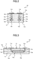
- a substrate for mounting a light-emitting element A2 as illustrated in FIG. 2 is modification 1 of an embodiment and FIG. 2 is a figure that corresponds to FIG. 1E .
- a width of a second conductor 16a is greater than that of a first conductor 15a.
- a width of the second conductor 16a is greater than that of the first conductor 15a, so that it is possible to cause heat that is generated from a light-emitting element 30 that is mounted on a terminal for an element 11a to escape to a back surface 10b with a high heat release property more efficiently.
- a width of the second conductor 16a is greater than that of the first conductor 15a, so that it is possible to further reduce a stress that is generated between a set of the first conductor 15a and the second conductor 16a and a substrate 10. Therefore, according to an embodiment, it is possible to further improve a reliability of the substrate for mounting a light-emitting element A2. This is caused by increasing of a rate of a metal with a near coefficient of thermal expansion at a position that is close to a heat release member on the substrate 10 in a case where such a heat release member is composed of a metal.
- a substrate for mounting a light-emitting element A3 as illustrated in FIG. 3 is modification 2 of an embodiment and FIG. 3 is a figure that corresponds to FIG. 1B .
- modification 2 as illustrated in FIG. 3 in a case where a substrate 10 is provided in a top view, a first via conductor 17a and a third via conductor 19a are arranged at different positions and a second via conductor 18a and a fourth via conductor 20a are arranged at different positions.
- the third via conductor 19a is arranged on a side of a terminal for a power source 12a with respect to the first via conductor 17a and the fourth via conductor 20a is arranged on a side of a terminal for an element 11a with respect to the second via conductor 18a.
- modification 2 when another mounting component such as an IC (Integrated Circuit) is packaged on a side of a front surface 10a or a side of a back surface 10b of the substrate 10, it is possible to increase a distance between a packaging surface and a second conductor 16a. Therefore, according to modification 2, it is possible to reduce an influence of a noise from another mounting component.
- IC Integrated Circuit
- a substrate for mounting a light-emitting element as illustrated in FIG. 4 is modification 3 of an embodiment and FIG. 4 is a figure that corresponds to FIG. 1B .
- modification 3 as illustrated in FIG. 4 configurations of a first conductor 15a, a second conductor 16a, and a first via conductor 17a are different from those of modification 2 as described above.
- first via conductor 17a is not connected to the first conductor 15a but is connected to the second conductor 16a.
- a wiring part 14a in modification 3 has the first via conductor 17a that connects a terminal for an element 11a and the second conductor 16a, a second via conductor 18a that connects a terminal for a power source 12a and the first conductor 15a, and a third via conductor 19a and a fourth via conductor 20a that connect the first conductor 15a and the second conductor 16a.
- FIG. 4 illustrates an example where the first via conductor 17a is connected to the second conductor 16a and the second via conductor 18a is connected to the first conductor 15a
- the first via conductor 17a may be connected to the first conductor 15a
- the second via conductor 18a may be connected to the second conductor 16a.
- first via conductor 17a is connected to the terminal for an element 11a and one of the first conductor 15a and the second conductor 16a and the second via conductor 18a is connected to the terminal for a power source 12a and another of the first conductor 15a and the second conductor 16a.
- a substrate for mounting a light-emitting element as illustrated in FIG. 5 is modification 4 of an embodiment and FIG. 5 is a figure that corresponds to FIG. 1B .
- modification 4 as illustrated in FIG. 5 configurations of a first conductor 15a, a second conductor 16a, and a second via conductor 18a are different from those of modification 3 as described above.
- a wiring part 14a in modification 4 has a first via conductor 17a that connects a terminal for an element 11a and the second conductor 16a, the second via conductor 18a that connects a terminal for a power source 12a and the second conductor 16a, and a third via conductor 19a and a fourth via conductor 20a that connect the first conductor 15a and the second conductor 16a.
- modification 4 when another mounting component such as an IC is packaged on a side of a front surface 10a or a side of a back surface 10b of a substrate 10, it is possible to increase a distance between a packaging surface and the first conductor 15a. Therefore, according to modification 4, it is possible to reduce an influence of a noise from another mounting component.
- a substrate for mounting a light-emitting element A6 as illustrated in FIG. 6 is modification 5 of an embodiment and FIG. 6 is a figure that corresponds to FIG. 1B .
- modification 5 as illustrated in FIG. 6 in a case where a substrate 10 is bisected in a thickness direction thereof, any of a first conductor 15a and a second conductor 16a is arranged on a side of a front surface 10a.
- any of the first conductor 15a and the second conductor 16a is arranged between such a cross section S and the front surface 10a.
- a substrate for mounting a light-emitting element A7 as illustrated in FIG. 7A and FIG. 7B is modification 6 of an embodiment. Additionally, FIG. 7A is a figure that corresponds to FIG. 1B and FIG. 7B is a figure that corresponds to FIG. 1E . In modification 6 as illustrated in FIG. 7A and FIG. 7B , a third conductor 22a is further provided in addition to a first conductor 15a and a second conductor 16a.
- Such a third conductor 22a extends in substantially parallel to the second conductor 16a on an opposite side of a front surface 10a and is connected in parallel with the second conductor 16a through a sixth via conductor 23a and a seventh via conductor 24a.
- a wiring part 14a that is formed by three parallel wirings is connected between a terminal for an element 11a and a terminal for a power source 12a, so that it is possible to further reduce a wiring inductance of the wiring part 14a.
- modification 6 it is possible to further increase a cross-sectional area of a site of the wiring part 14a that extends in a surface direction (that is, the first conductor 15a, the second conductor 16a, and the third conductor 22a). Therefore, according to modification 6, it is possible to further reduce a wiring resistance of the wiring part 14a.
- the first conductor 15a, the second conductor 16a, and the third conductor 22a are arranged in such a manner that both parts with a less thickness face one another in upward and downward directions. Thereby, it is possible to provide the first conductor 15a, the second conductor 16a, and the third conductor 22a closely in a thickness direction of a substrate 10. Therefore, according to modification 6, it is possible to further reduce a wiring inductance of the wiring part 14a.
- the first conductor 15a, the second conductor 16a, and the third conductor 22a are formed so as to be of a ladder shape in a cross-sectional view, so that it is possible to further decrease deformation of an inside of the substrate 10 in a thickness direction thereof.
- the third conductor 22a is arranged at a position that is closer to a back surface 10b, so that it is possible to cause heat that is generated from the light-emitting element 30 that is mounted on the terminal for an element 11a to escape to the back surface 10b with a high heat release property more efficiently.
- a site that extends in a surface direction of the wiring part 14a is divided into the first conductor 15a, the second conductor 16a, and the third conductor 22a and a ceramic site is present therebetween, so that it is possible to further reduce a stress that is generated between a set of the first conductor 15a, the second conductor 16a, and the third conductor 22a, and the substrate 10.
- a via conductor other than the sixth via conductor 23a and the seventh via conductor 24a may be connected between the second conductor 16a and the third conductor 22a.
- an eighth via conductor 25a may be connected between a middle part of the second conductor 16a and a middle part of the third conductor 22a.
- FIGS. 8 to 10 are plan views where respective steps in a first half are viewed from above respectively and FIG. 11 is a cross-sectional view where respective steps in a second half are provided in a cross-sectional view from a side respectively.
- a substrate for mounting a light-emitting element A1 is formed by respectively applying a predetermined process to three green sheets, subsequently laminating the three green sheets, and finally firing a laminated molded body.
- each step in a first half for a green sheet 50 as an upper layer will be explained based on FIG. 8 that is provided as a plan view
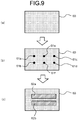
- each step in a first half for a green sheet 60 as a middle layer will be explained based on FIG. 9 that is provided as a plan view
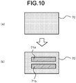
- each step in a first half for a green sheet 70 as a lower layer will be explained based on FIG. 10 that is provided as a plan view
- each step in a second half for the green sheets 50, 60, 70 will be explained based on FIG. 11 that is provided as a cross-sectional view.
- the green sheet 50 is prepared that is preliminarily processed into a predetermined shape. Then, a four predetermined locations on the green sheet 50 are punched into circular shapes in a plan view and four punched holes are respectively filled with via conductors 51a, 51b, 51c, 51d ((b) of FIG. 8 ).
- a conductor pattern 52a is printed so as to be linked to the via conductor 51a and a conductor pattern 52b is printed so as to be linked to the via conductor 51b.
- a conductor pattern 52c is printed so as to be linked to the via conductor 51c and a conductor pattern 52d is printed so as to be linked to the via conductor 51d.
- a conductor pattern 52e with a frame shape is printed so as to surround the conductor patterns 52a, 52b.
- the green sheet 60 is prepared that is preliminarily processed into a predetermined shape. Then, six predetermined locations on the green sheet 60 are punched into circular shapes in a plan view and six punched holes are respectively filled with via conductors 61a, 61b, 61c, 61d, 61e, 61f ((b) of FIG. 9 ).
- a conductor pattern 62a is printed so as to be linked to the via conductors 61a, 61c, 61e and a conductor pattern 62b is printed so as to be linked to the via conductors 61b, 61d, 61f.
- the green sheet 70 is prepared that is preliminarily processed into a predetermined shape. Then, as illustrated in (b) of FIG. 10 , on a top surface of the green sheet 70, conductor patterns 71a, 71b are printed. Additionally, the conductor pattern 71a is formed at a position that corresponds to the via conductors 61a, 61c, 61e that are provided on the green sheet 60 and the conductor pattern 71b is formed at a position that corresponds to the via conductors 61b, 61d, 61f that are provided on the green sheet 60.
- FIG. 11 that illustrates subsequent steps is a cross-sectional view that is viewed along an arrow of line E-E as illustrated in (c) of FIG. 8 .
- the green sheet 50, the green sheet 60, and the green sheet 70 are sequentially laminated from above, and heating and pressurizing are executed to form a lamination molded body 80 ((b) of FIG. 11 ).
- the conductor patterns 52a, 52c, 52e are sites that correspond to a terminal for an element 11a, a terminal for a power source 12a, and a metal film for sealing 13 of the substrate for mounting a light-emitting element A1, respectively
- the via conductors 51a, 51c are sites that correspond to a first via conductor 17a and a second via conductor 18a of the substrate for mounting a light-emitting element A1, respectively.
- the conductor pattern 62a is a site that corresponds to a first conductor 15a of the substrate for mounting a light-emitting element A1 and the via conductors 61a, 61c, 61e are sites that correspond to a third via conductor 19a, a fourth via conductor 20a, and a fifth via conductor 21a of the substrate for mounting a light-emitting element A1, respectively.
- the conductor pattern 71a is a site that corresponds to a second conductor 16a of the substrate for mounting a light-emitting element A1.
- the conductor patterns 52b, 52d are sites that correspond to a terminal for an element 11b and a terminal for a power source 12b of the substrate for mounting a light-emitting element A1, respectively, and the via conductors 51b, 51d are sites that correspond to a first via conductor 17b and a second via conductor 18b of the substrate for mounting a light-emitting element A1, respectively.
- the conductor pattern 62b is a site that corresponds to a first conductor 15b of the substrate for mounting a light-emitting element A1 and the via conductors 61b, 61d, 61f are sites that correspond to a third via conductor 19b, a fourth via conductor 20b, and a fifth via conductor 21b of the substrate for mounting a light-emitting element A1, respectively.
- the conductor pattern 71b is a site that corresponds to a second conductor 16b of the substrate for mounting a light-emitting element A1.
- the lamination molded body 80 that is formed like (b) of FIG. 11 is fired at a high temperature (1700 °C to 2000 °C), so that the substrate for mounting a light-emitting element A1 is completed.
- a basic structure for the green sheets 50, 60, 70 that are used in a manufacturing process as described above is, for example, an inorganic powder where a powder that is composed of yttria (Y 2 O 3 ), calcia (CaO), erbia (Er 2 O 3 ), or the like, as a sintering aid, is mixed to a powder of aluminum nitride that is a main raw material. Then, an organic vehicle is added and mixed to such an inorganic powder so as to be slurry-like and a conventionally well-known doctor blade method or calendar roll method is used for it, so that the green sheet 50 is formed.
- a powder that is composed of yttria (Y 2 O 3 ), calcia (CaO), erbia (Er 2 O 3 ), or the like as a sintering aid
- the conductor patterns 52a to 52e, 62a, 62b, 71a, 71b or the via conductors 51a to 51d, 61a to 61f are formed from, for example, a paste where aluminum nitride, an organic binder, a solvent, or the like, as a co-agent, is mixed to molybdenum (Mo) or tungsten (W) as a high-melting-point metal that is a main raw material.
- Mo molybdenum
- W tungsten
- a low-melting-point metal such as copper that is included in a high-melting-point metal as described above may be used depending on a firing temperature of a ceramic(s).
- the present invention is not limited to an embodiment as described above and a variety of modifications are allowed unless departing from a spirit thereof.
- the wiring part 14a may be composed of a four-or-more-layered structure.
- positions where the terminals for a power source 12a, 12b are provided thereat are not limited to the front surface 10a of the substrate 10 and it is sufficient that they are provided on a surface of the substrate 10 such as the back surface 10b, the end surface 10c, or the side surface 10d of the substrate 10.
- the light-emitting element 30 or the like is air-tightly sealed by using the cap 40 in an embodiment as described above, an air-tightly sealing member is not limited to the cap 40.
- the light-emitting element 30 or the like may be air-tightly sealed by combining a seal ring (a sealing member) with a frame shape where a side window is provided at a predetermined position, and a lid body with a plate shape.
- a substrate for mounting a light-emitting element A1 (A2 to A7) according to an embodiment includes a substrate 10 that is composed of a ceramic(s), a terminal for an element 11a that is provided on a front surface 10a of the substrate 10 where a light-emitting element 30 is mounted thereon, a terminal for a power source 12a that is provided on the substrate 10 where an external power source is connected thereto, and a wiring part 14a that is provided inside the substrate 10 and electrically connects the terminal for an element 11a and the terminal for a power source 12a.
- the wiring part 14a has a first conductor 15a that extends in a surface direction of the substrate 10 and a second conductor 16a that extends in substantially parallel to the first conductor 15a on an opposite side of the front surface 10a and is connected in parallel with the first conductor 15a.
- the wiring part 14a has a first via conductor 17a that extends in a thickness direction of the substrate 10 and connects the terminal for an element 11a and the first conductor 15a, a second via conductor 18a that extends in a thickness direction of the substrate 10 and connects the terminal for a power source 12a and the first conductor 15a, and a third via conductor 19a and a fourth via conductor 20a that extend in a thickness direction of the substrate 10 and connect the first conductor 15a and the second conductor 16a.
- a first via conductor 17a that extends in a thickness direction of the substrate 10 and connects the terminal for an element 11a and the first conductor 15a
- a second via conductor 18a that extends in a thickness direction of the substrate 10 and connects the terminal for a power source 12a and the first conductor 15a
- a third via conductor 19a and a fourth via conductor 20a that extend in a thickness direction of the substrate 10 and connect the first conductor 15a and the second conductor 16a
- the first via conductor 17a and the third via conductor 19a are arranged at substantially identical positions and the second via conductor 18a and the fourth via conductor 20a are arranged at substantially identical positions.
- the first via conductor 17a and the third via conductor 19a are arranged at different positions and the second via conductor 18a and the fourth via conductor 20a are arranged at different positions.
- a wiring part 14a with a single wire structure with an equal length or thickness at a part near a terminal for an element 11a or a terminal for a power source 12a, so that, when a light-emitting element 30 is pulse-driven by an external power source, it is possible to prevent or reduce a variation of a pulsed current.
- the wiring part 14a has a first via conductor 17a that extends in a thickness direction of the substrate 10 and connects the terminal for an element 11a and one of the first conductor 15a and the second conductor 16a, a second via conductor 18a that extends in a thickness direction of the substrate 10 and connects the terminal for a power source 12a and another of the first conductor 15a and the second conductor 16a, and a third via conductor 19a and a fourth via conductor 20a that extend in a thickness direction of the substrate 10 and connect the first conductor 15a and the second conductor 16a.
- a light-emitting element 30 when a light-emitting element 30 is pulse-driven by an external power source, it is possible to prevent or reduce causing of a phase difference in a pulsed current, so that it is possible to improve a grade of light emission of a light-emitting device.
- lengths of the first conductor 15a that extends between the third via conductor 19a and the fourth via conductor 20a and the second conductor 16a that extends between the third via conductor 19a and the fourth via conductor 20a are substantially equal.
- the wiring part 14a has a first via conductor 17a that extends in a thickness direction of the substrate 10 and connects the terminal for an element 11a and the second conductor 16a, a second via conductor 18a that extends in a thickness direction of the substrate 10 and connects the terminal for a power source 12a and the second conductor 16a, and a third via conductor 19a and a fourth via conductor 20a that extend in a thickness direction of the substrate 10 and connect the first conductor 15a and the second conductor 16a.
- a width of the second conductor 16a is greater than that of the first conductor 15a.
- any of the first conductor 15a and the second conductor 16a is arranged on a side of the front surface 10a. Thereby, it is possible to further reduce a wiring inductance of a wiring part 14a.
- the wiring part 14a has a third conductor 22a that extends in substantially parallel to the second conductor 16a on an opposite side of the front surface 10a and is connected in parallel with the second conductor 16a. Thereby, it is possible to further reduce a wiring resistance of a wiring part 14a.
- a light-emitting device includes the substrate for mounting a light-emitting element A1 (A2 to A7) as described above, and a light-emitting element 30 that is mounted on the terminal for an element 11a of the substrate for mounting a light-emitting element A1 (A2 to A7).
- a light-emitting device includes the substrate for mounting a light-emitting element A1 (A2 to A7) as described above, and a light-emitting element 30 that is mounted on the terminal for an element 11a of the substrate for mounting a light-emitting element A1 (A2 to A7).
Landscapes
- Physics & Mathematics (AREA)
- Condensed Matter Physics & Semiconductors (AREA)
- General Physics & Mathematics (AREA)
- Electromagnetism (AREA)
- Optics & Photonics (AREA)
- Engineering & Computer Science (AREA)
- Microelectronics & Electronic Packaging (AREA)
- Led Device Packages (AREA)
- Structure Of Printed Boards (AREA)
- Semiconductor Lasers (AREA)
- Production Of Multi-Layered Print Wiring Board (AREA)
- Printing Elements For Providing Electric Connections Between Printed Circuits (AREA)
Abstract
Description
- Disclosed embodiments relate to a substrate for mounting a light-emitting element and a light-emitting device.
- A substrate that has a light-emitting element connection terminal pad and an external connection terminal pad that are formed on an insulated substrate and a conductor wiring that is formed on the insulated substrate and is electrically connected between both such pads has conventionally been known as a substrate for mounting a light-emitting element to mount a light-emitting element (see, for example, Patent Literature 1).
- Patent Literature 1: Japanese Patent Application Publication No.
2010-199167 - A substrate for mounting a light-emitting element according to an aspect of an embodiment includes a substrate that is composed of a ceramic(s), a terminal for an element that is provided on a front surface of the substrate where a light-emitting element is mounted thereon, a terminal for a power source that is provided on the substrate where an external power source is connected thereto, and a wiring part that is provided inside the substrate and electrically connects the terminal for an element and the terminal for a power source. Furthermore, the wiring part has a first conductor that extends in a surface direction of the substrate, and a second conductor that extends in substantially parallel to the first conductor on an opposite side of the front surface and is connected in parallel with the first conductor.
- Furthermore, a light-emitting device according to an aspect of an embodiment includes the substrate for mounting a light-emitting element as described above, and a light-emitting element that is mounted on the terminal for an element of the substrate for mounting a light-emitting element.
-
-
FIG. 1A is a perspective view of a substrate for mounting a light-emitting element according to an embodiment. -
FIG. 1B is a cross-sectional view that is viewed along an arrow of line A-A as illustrated inFIG. 1A . -
FIG. 1C is a cross-sectional view that is viewed along an arrow of line B-B as illustrated inFIG. 1A . -
FIG. 1D is a cross-sectional view that is viewed along an arrow of line C-C as illustrated inFIG. 1A . -
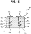
FIG. 1E is a cross-sectional view that is viewed along an arrow of line D-D as illustrated inFIG. 1A . -
FIG. 2 is a cross-sectional view of a substrate for mounting a light-emitting element according to modification 1 of an embodiment. -
FIG. 3 is a cross-sectional view of a substrate for mounting a light-emitting element according to modification 2 of an embodiment. -
FIG. 4 is a cross-sectional view of a substrate for mounting a light-emitting element according to modification 3 of an embodiment. -
FIG. 5 is a cross-sectional view of a substrate for mounting a light-emitting element according to modification 4 of an embodiment. -
FIG. 6 is a cross-sectional view of a substrate for mounting a light-emitting element according to modification 5 of an embodiment. -
FIG. 7A is a cross-sectional view of a substrate for mounting a light-emitting element according to modification 6 of an embodiment. -
FIG. 7B is another cross-sectional view of a substrate for mounting a light-emitting element according to modification 6 of an embodiment. -
FIG. 8 is a plan view that illustrates a manufacturing process for a substrate for mounting a light-emitting element according to an embodiment. -
FIG. 9 is a plan view that illustrates another manufacturing process for a substrate for mounting a light-emitting element according to an embodiment. -
FIG. 10 is a plan view that illustrates another manufacturing process for a substrate for mounting a light-emitting element according to an embodiment. -
FIG. 11 is a cross-sectional view that illustrates another manufacturing process for a substrate for mounting a light-emitting element according to an embodiment. Description of Embodiments - In a conventional technique as described above, it is difficult to reduce an inductance of a wiring conductor, so that a pulse waveform may decay from a rectangular shape when a light-emitting element is pulse-driven by an external power source. Hence, a great variation in an output of light emission of a light-emitting element may be caused. An aspect of an embodiment as illustrated below is provided by taking the above into consideration.
- Hereinafter, embodiments of a substrate for mounting a light-emitting element and a light-emitting device as disclosed in the present application will be explained with reference to the accompanying drawings. Additionally, this invention is not limited to a substrate for mounting a light-emitting element or a light-emitting device, and it goes without saying that it is possible to apply it to a substrate or device that mounts a general electrical element that has a heat generation property, other than a light-emitting element.
- Herein, for an electrical element that has a heat generation property, it is possible to provide a large scale integrated circuit (LSI: Large Scale Integrated circuit), a charge coupled device (CCD: Charge Coupled Device), a laser diode (Laser Diode), a light-emitting diode (LED: Light Emitting Diode), and the like. An embodiment as illustrated below is useful, inter alia, for a laser diode.
- First, an outlie of a substrate for mounting a light-emitting element A1 according to an embodiment will be explained with reference to
FIG. 1A to FIG. 1E . As illustrated inFIG. 1A , a substrate for mounting a light-emitting element A1 according to an embodiment includes asubstrate 10 with a flat plate shape that is composed of a ceramic(s). Furthermore, terminals for anelement front surface 10a of such asubstrate 10. Furthermore, terminals for apower source substrate 10. Additionally, in such a case, althoughFIG. 1A illustrates a structure where the terminals for anelement power source front surface 10a of thesubstrate 10, thefront surface 10a of thesubstrate 10 is not limiting and the terminals for apower source end surface 10c or aside surface 10d of thesubstrate 10. - The terminal for an
element 11a is a terminal where a light-emittingelement 30 is mounted thereon. The terminal for anelement 11b is a terminal where the light-emittingelement 30 that is mounted on the terminal for anelement 11a is connected thereto by a bonding wire or the like. Furthermore, the terminals for apower source - Then, as illustrated in
FIG. 1B to FIG. 1E , the terminal for anelement 11a and the terminal for apower source 12a are electrically connected through awiring part 14a and the terminal for anelement 11b and the terminal for apower source 12b are electrically connected through awiring part 14b. - As illustrated in
FIG. 1B , thewiring part 14a is formed inside thesubstrate 10 and has afirst conductor 15a, asecond conductor 16a, afirst via conductor 17a, asecond via conductor 18a, a third viaconductor 19a, and afourth via conductor 20a. - Furthermore, as illustrated in
FIG. 1C , thewiring part 14b is also formed inside thesubstrate 10 and has afirst conductor 15b, asecond conductor 16b, a first viaconductor 17b, a second viaconductor 18b, a third viaconductor 19b, and a fourth viaconductor 20b. - Additionally, the
wiring part 14b has a configuration similar to that of thewiring part 14a, so that a configuration of thewiring part 14a will be explained in the following explanation and an explanation of thewiring part 14b will be omitted therein. - Any of the
first conductor 15a and thesecond conductor 16a is composed of a metal and extends in a surface direction of the substrate 10 (that is, substantially parallel to thefront surface 10a of the substrate 10). In other words, thefirst conductor 15a and thesecond conductor 16a extend so as to be along thefront surface 10a of thesubstrate 10. Furthermore, any of thefirst conductor 15a and thesecond conductor 16a extends in such a manner that one end side thereof reaches a lower side of the terminal for anelement 11a, and extends in such a manner that another end side thereof reaches a lower side of the terminal for apower source 12a. That is, thefirst conductor 15a and thesecond conductor 16a are arranged side by side inside thesubstrate 10 in a thickness direction thereof (that is, substantially perpendicular to thefront surface 10a of the substrate 10). Herein, "being composed of a metal" means that, for example, a ceramic(s) other than a metal may be included partially. A similar meaning also applies below. - Furthermore, the
second conductor 16a is arranged on an opposite side of thefront surface 10a with respect to thefirst conductor 15a. That is, thesecond conductor 16a is arranged so as to be more distant from thefront surface 10a than thefirst conductor 15a. - Any of the first via
conductor 17a to the fourth viaconductor 20a is composed of a metal and extends in a thickness direction of thesubstrate 10. The first viaconductor 17a is arranged on a lower side of the terminal for anelement 11a and is connected between such a terminal for anelement 11a and thefirst conductor 15a. The second viaconductor 18a is arranged on a lower side of the terminal for apower source 12a and is connected between such a terminal for apower source 12a and thefirst conductor 15a. - The third via
conductor 19a is arranged on a lower side of the terminal for anelement 11a and is connected between thefirst conductor 15a and thesecond conductor 16a. The fourth viaconductor 20a is arranged on a lower side of the terminal for apower source 12a and is connected between thefirst conductor 15a and thesecond conductor 16a. - As explained thus far, the
wiring part 14a has a wiring that sequentially wire-connects the first viaconductor 17a, thefirst conductor 15a, and the second viaconductor 18a and a wiring that sequentially wire-connects the first viaconductor 17a, thefirst conductor 15a, the third viaconductor 19a, thesecond conductor 16a, the fourth viaconductor 20a, thefirst conductor 15a, and the second viaconductor 18a. That is, thewiring part 14a where wirings are formed in parallel is connected between the terminal for anelement 11a and the terminal for apower source 12a. - Thereby, it is possible to reduce a wiring inductance of the
wiring part 14a as compared with a case where thewiring part 14a is a wiring that is a single wire. Therefore, according to an embodiment, it is possible to maintain a pulse waveform in a state that is close to a rectangular shape when the light-emittingelement 30 is pulse-driven by an external power source that is connected to the terminals for apower source element 30. - Furthermore, in an embodiment, it is possible to increase a cross-sectional area of a site of the
wiring part 14a that extends in a surface direction (that is, thefirst conductor 15a and thesecond conductor 16a). Therefore, according to an embodiment, it is possible to reduce a wiring resistance of thewiring part 14a. - Furthermore, in an embodiment, as illustrated in
FIG. 1E , thefirst conductor 15a and thesecond conductor 16a are arranged in such a manner that both parts with a less thickness face one another in upward and downward directions. Thereby, it is possible to provide thefirst conductor 15a and thesecond conductor 16a closely in a thickness direction of thesubstrate 10. Therefore, according to an embodiment, it is possible to further reduce a wiring resistance of thewiring part 14a. - Furthermore, in an embodiment, as illustrated in
FIG. 1B , a ceramic site of thesubstrate 10 is present between thefirst conductor 15a and thesecond conductor 16a. If thefirst conductor 15a and thesecond conductor 16a are integrated and thewiring part 14a is composed of a thick conductor that extends in a surface direction, there is a great difference in a coefficient of thermal expansion between a thick conductor of a metal and thesubstrate 10 of a ceramic(s), so that a great stress may be generated between the thick conductor and thesubstrate 10. Therefore, in such a case, a reliability of the substrate for mounting a light-emitting element A1 may be degraded. - However, in an embodiment, a site of the
wiring part 14a that extends in a surface direction is divided into thefirst conductor 15a and thesecond conductor 16a and a ceramic site is present therebetween, so that it is possible to reduce a stress that is generated between a set of thefirst conductor 15a and thesecond conductor 16a and thesubstrate 10. Therefore, according to an embodiment, it is possible to improve a reliability of the substrate for mounting a light-emitting element A1. - Furthermore, in an embodiment, it is possible to arrange the
second conductor 16a with a high thermal conductivity at a position that is close to aback surface 10b of thesubstrate 10. Additionally, theback surface 10b is a surface of thesubstrate 10 on an opposite side of thefront surface 10a. - Thereby, it is possible to cause heat that is generated from the light-emitting
element 30 that is mounted on the terminal for anelement 11a to efficiently escape to theback surface 10b with a large surface area and a high heat release property through the first viaconductor 17a, the third viaconductor 19a, and thesecond conductor 16a that extend in a thickness direction. Therefore, according to an embodiment, for example, in a case where a heat release member of a fin type or the like is placed on theback surface 10b, it is possible to increase a thermal conductivity to such a heat release member. - Furthermore, in an embodiment, in a case where the
substrate 10 is provided in a top view, the first viaconductor 17a and the third viaconductor 19a are arranged at substantially identical positions, and the second viaconductor 18a and the fourth viaconductor 20a are arranged at substantially identical positions. Thereby, it is possible to increase lengths of sites of thewiring part 14a that are connected in parallel by thefirst conductor 15a and thesecond conductor 16a. Therefore, according to an embodiment, it is possible to further reduce a wiring resistance of thewiring part 14a. - Herein, the first via
conductor 17a and the third viaconductor 19a being arranged at substantially identical positions refers to a state where a site that overlaps in a thickness direction of thesubstrate 10 is present between the first viaconductor 17a and the third viaconductor 19a. A similar matter is also applied between the second viaconductor 18a and the fourth viaconductor 20a. Furthermore, it is preferable that lengths of thefirst conductor 15a and thesecond conductor 16a are substantially equal. Herein, a length between thefirst conductor 15a and thesecond conductor 16a being substantially equal refers to a case where a difference in a length between thefirst conductor 15a and thesecond conductor 16a is less than or equal to a diameters of via conductors that are provided on both ends of such afirst conductor 15a and asecond conductor 16a. A diameter of a via conductor is a minimum diameter among diameters of the first viaconductor 17a, the second viaconductor 18a, the third viaconductor 19a, and the fourth viaconductor 20a. - Furthermore, in an embodiment, a via conductor other than the third via
conductor 19a and the fourth viaconductor 20a may be connected between thefirst conductor 15a and thesecond conductor 16a. For example, as illustrated inFIG. 1B , a fifth viaconductor 21a may be connected between a middle part of thefirst conductor 15a and a middle part of thesecond conductor 16a. Thereby, it is possible to further equalize a current that flows through thefirst conductor 15a and a current that flows through thesecond conductor 16a. - Furthermore, as illustrated in
FIG. 1C , a fifth viaconductor 21b may be connected between a middle part of thefirst conductor 15b and a middle part of thesecond conductor 16b. Thereby, it is possible to further equalize a current that flows through thefirst conductor 15b and a current that flows through thesecond conductor 16b. - Furthermore, in an embodiment, it is preferable that any of the
first conductor 15a and thesecond conductor 16a is arranged to be substantially parallel to thefront surface 10a. Thereby, it is possible to arrange thefirst conductor 15a and thesecond conductor 16a more closely. - Subsequently, a more detailed configuration of the substrate for mounting a light-emitting element A1 will be explained with reference to
FIG. 1A . - The
substrate 10 is formed of a ceramic(s). For such a ceramic(s), for example, alumina, silica, mullite, cordierite, forsterite, aluminum nitride, silicon nitride, silicon carbide, a glass ceramic(s), or the like is suitable. Furthermore, it is preferable that thesubstrate 10 includes aluminum nitride (AlN) as a main component, from the viewpoint of a high thermal conductivity and a coefficient of thermal expansion that is close to that of the light-emittingelement 30. - Herein, "including aluminum nitride as a main component" refers to the
substrate 10 including 80% by mass or more of aluminum nitride. In a case where 80% by mass or more of aluminum nitride is included in thesubstrate 10, a thermal conductivity of the substrate for mounting a light-emitting element A1 is increased, so that it is possible to improve a heat release property thereof. - Moreover, it is preferable that the
substrate 10 includes 90% by mass or more of aluminum nitride. As a content of aluminum nitride is 90% by mass or more, it is possible for a thermal conductivity of thesubstrate 10 to be 150 W/mK or greater, so that it is possible to realize the substrate for mounting a light-emitting element A1 with an excellent heat release property. - It is sufficient that the terminals for an
element substrate 10, with a high strength, so that it is possible to realize the substrate for mounting a light-emitting element A1 with a high reliability. - Furthermore, a plating film of Ni or the like may be formed on a surface of such a metallized film. Moreover, a solder or an Au-Sn plating film may be provided on a surface of such a plating film.
- A metal film for sealing 13 is provided on the
front surface 10a of thesubstrate 10 so as to surround the terminals for anelement cap 40 is provided so as to cover the light-emittingelement 30 that is mounted on the terminal for anelement 11a, such acap 40 is bonded thereto. - Furthermore, it is preferable that the terminals for a
power source element power source conductor 17a to the fourth viaconductor 20a are also metallized films where a metal powder is fired. - A light-emitting device is configured in such a manner that the light-emitting
element 30 and thecap 40 are mounted on the substrate for mounting a light-emitting element A1 as explained thus far. - For the light-emitting
element 30, it is possible to use, for example, a semiconductor laser (that is also referred to as a laser diode) or the like. The light-emittingelement 30 is arranged in such a manner that an emittingsurface 30a that is provided on one end surface thereof is oriented in a predetermined direction of the substrate for mounting a light-emitting element A1. - The light-emitting
element 30 is bonded to the terminal for anelement 11a on thesubstrate 10 by using an electrically conductive bonding material such as a solder. In such a case, a (non-illustrated) first electrode that is provided on a bottom surface of the light-emittingelement 30 and the terminal for anelement 11a are electrically connected by such an electrically conductive bonding material. - Moreover, a (non-illustrated) second electrode that is provided on a top surface of the light-emitting
element 30 and the terminal for anelement 11b that is adjacent to the terminal for anelement 11a are electrically connected by using a (non-illustrated) bonding wire or the like. - The
cap 40 is a member for air-tightly sealing an area that is surrounded by the metal film for sealing 13, such as the light-emittingelement 30. It is possible to provide thecap 40 that is composed of a metallic material, a ceramic(s), or the like, and it is sufficient that it is composed of, for example, kovar (an Fe-Ni-Co alloy) from the viewpoint of a heat resistance and a heat release property that are high. - A
side window 41 is provided on a side surface of thecap 40 and a transparent glass is put in theside window 41. Thecap 40 is arranged in such a manner that theside window 41 is oriented in a direction that is identical to that of the emittingsurface 30a of the light-emittingelement 30. Then, light that is emitted from the emittingsurface 30a passes through theside window 41 and is emitted externally. - For bonding of the
cap 40 and the metal film for sealing 13, it is preferable to use a wax material. As a wax material is used for a bonding material, it is possible to increase an airtightness of an area that is sealed by thecap 40, so that it is possible to improve a reliability of a light-emitting device. - Next, a variety of modifications of an embodiment will be explained with reference to
FIG. 2 to FIG. 7B . Additionally, a component that is common to that of an embodiment as described above will be provided with an identical sign and a detailed explanation thereof will be omitted, in the following explanation. - A substrate for mounting a light-emitting element A2 as illustrated in
FIG. 2 is modification 1 of an embodiment andFIG. 2 is a figure that corresponds toFIG. 1E . In modification 1 as illustrated inFIG. 2 , a width of asecond conductor 16a is greater than that of afirst conductor 15a. - Thus, in modification 1, a width of the
second conductor 16a is greater than that of thefirst conductor 15a, so that it is possible to cause heat that is generated from a light-emittingelement 30 that is mounted on a terminal for anelement 11a to escape to aback surface 10b with a high heat release property more efficiently. - Therefore, according to modification 1, in a case where a heat release member of a fin type or the like is placed on the
back surface 10b, it is possible to further improve a heat conductivity to such a heat release member. - Furthermore, in modification 1, a width of the
second conductor 16a is greater than that of thefirst conductor 15a, so that it is possible to further reduce a stress that is generated between a set of thefirst conductor 15a and thesecond conductor 16a and asubstrate 10. Therefore, according to an embodiment, it is possible to further improve a reliability of the substrate for mounting a light-emitting element A2. This is caused by increasing of a rate of a metal with a near coefficient of thermal expansion at a position that is close to a heat release member on thesubstrate 10 in a case where such a heat release member is composed of a metal. - A substrate for mounting a light-emitting element A3 as illustrated in
FIG. 3 is modification 2 of an embodiment andFIG. 3 is a figure that corresponds toFIG. 1B . In modification 2 as illustrated inFIG. 3 , in a case where asubstrate 10 is provided in a top view, a first viaconductor 17a and a third viaconductor 19a are arranged at different positions and a second viaconductor 18a and a fourth viaconductor 20a are arranged at different positions. - Specifically, the third via
conductor 19a is arranged on a side of a terminal for apower source 12a with respect to the first viaconductor 17a and the fourth viaconductor 20a is arranged on a side of a terminal for anelement 11a with respect to the second viaconductor 18a. - Thereby, at a part near the terminal for an
element 11a or the terminal for apower source 12a, it is possible to provide afirst conductor 15a at a part of awiring part 14a that is close to the first viaconductor 17a and the second viaconductor 18a, with a single wire structure with an equal length or thickness. Therefore, according to modification 2, it is possible to prevent or reduce a variation of a pulsed current when a light-emittingelement 30 is pulse-driven by an external power source. - Furthermore, in modification 2, when another mounting component such as an IC (Integrated Circuit) is packaged on a side of a
front surface 10a or a side of aback surface 10b of thesubstrate 10, it is possible to increase a distance between a packaging surface and asecond conductor 16a. Therefore, according to modification 2, it is possible to reduce an influence of a noise from another mounting component. - A substrate for mounting a light-emitting element as illustrated in
FIG. 4 is modification 3 of an embodiment andFIG. 4 is a figure that corresponds toFIG. 1B . In modification 3 as illustrated inFIG. 4 , configurations of afirst conductor 15a, asecond conductor 16a, and a first viaconductor 17a are different from those of modification 2 as described above. - Specifically, while one end side of the
first conductor 15a does not reach a lower side of the first viaconductor 17a, one end side of thesecond conductor 16a reaches the lower side of the first viaconductor 17a. Then, the first viaconductor 17a is not connected to thefirst conductor 15a but is connected to thesecond conductor 16a. - In other words, a
wiring part 14a in modification 3 has the first viaconductor 17a that connects a terminal for anelement 11a and thesecond conductor 16a, a second viaconductor 18a that connects a terminal for apower source 12a and thefirst conductor 15a, and a third viaconductor 19a and a fourth viaconductor 20a that connect thefirst conductor 15a and thesecond conductor 16a. - Thereby, it is possible to match lengths of two wirings that are formed in parallel in the
wiring part 14a. Specifically, it is possible to match a length of a wiring that sequentially wire-connects the first viaconductor 17a, thesecond conductor 16a, the third viaconductor 19a, thefirst conductor 15a, and the second viaconductor 18a and a length of a wiring that sequentially wire-connects the first viaconductor 17a, thesecond conductor 16a, the fourth viaconductor 20a, thefirst conductor 15a, and the second viaconductor 18a. - Thereby, when a light-emitting
element 30 is pulse-driven by an external power source, it is possible to prevent or reduce causing of a phase difference in a pulsed current. Therefore, according to modification 3, it is possible to improve a grade of light emission of a light-emitting device. - Additionally, although
FIG. 4 illustrates an example where the first viaconductor 17a is connected to thesecond conductor 16a and the second viaconductor 18a is connected to thefirst conductor 15a, the first viaconductor 17a may be connected to thefirst conductor 15a and the second viaconductor 18a may be connected to thesecond conductor 16a. - That is, in modification 3, it is sufficient that the first via
conductor 17a is connected to the terminal for anelement 11a and one of thefirst conductor 15a and thesecond conductor 16a and the second viaconductor 18a is connected to the terminal for apower source 12a and another of thefirst conductor 15a and thesecond conductor 16a. - A substrate for mounting a light-emitting element as illustrated in
FIG. 5 is modification 4 of an embodiment andFIG. 5 is a figure that corresponds toFIG. 1B . In modification 4 as illustrated inFIG. 5 , configurations of afirst conductor 15a, asecond conductor 16a, and a second viaconductor 18a are different from those of modification 3 as described above. - Specifically, while another end side of the
first conductor 15a does not reach a lower side of the second viaconductor 18a, another end side of thesecond conductor 16a reaches the lower side of the second viaconductor 18a. Then, the second viaconductor 18a is not connected to thefirst conductor 15a but is connected to thesecond conductor 16a. - In other words, a
wiring part 14a in modification 4 has a first viaconductor 17a that connects a terminal for anelement 11a and thesecond conductor 16a, the second viaconductor 18a that connects a terminal for apower source 12a and thesecond conductor 16a, and a third viaconductor 19a and a fourth viaconductor 20a that connect thefirst conductor 15a and thesecond conductor 16a. - Thereby, at a part near the terminal for an
element 11a or the terminal for apower source 12a, it is possible to provide thewiring part 14a with a single wire structure with an equal length or thickness. Therefore, according to modification 4, when a light-emittingelement 30 is pulse-driven by an external power source, it is possible to prevent or reduce a variation of a pulsed current. - Furthermore, in modification 4, when another mounting component such as an IC is packaged on a side of a
front surface 10a or a side of aback surface 10b of asubstrate 10, it is possible to increase a distance between a packaging surface and thefirst conductor 15a. Therefore, according to modification 4, it is possible to reduce an influence of a noise from another mounting component. - A substrate for mounting a light-emitting element A6 as illustrated in
FIG. 6 is modification 5 of an embodiment andFIG. 6 is a figure that corresponds toFIG. 1B . In modification 5 as illustrated inFIG. 6 , in a case where asubstrate 10 is bisected in a thickness direction thereof, any of afirst conductor 15a and asecond conductor 16a is arranged on a side of afront surface 10a. - In other words, as illustrated in
FIG. 6 , in a case where a cross section S is defined that bisects thesubstrate 10 in a thickness direction thereof, any of thefirst conductor 15a and thesecond conductor 16a is arranged between such a cross section S and thefront surface 10a. - Thereby, it is possible to decrease a total length of a
wiring part 14a that is connected between a terminal for anelement 11a and a terminal for apower source 12a. Therefore, according to modification 5, it is possible to further reduce a wiring inductance of thewiring part 14a. - A substrate for mounting a light-emitting element A7 as illustrated in
FIG. 7A and FIG. 7B is modification 6 of an embodiment. Additionally,FIG. 7A is a figure that corresponds toFIG. 1B andFIG. 7B is a figure that corresponds toFIG. 1E . In modification 6 as illustrated inFIG. 7A and FIG. 7B , athird conductor 22a is further provided in addition to afirst conductor 15a and asecond conductor 16a. - Such a
third conductor 22a extends in substantially parallel to thesecond conductor 16a on an opposite side of afront surface 10a and is connected in parallel with thesecond conductor 16a through a sixth viaconductor 23a and a seventh viaconductor 24a. - Then, in modification 6, a
wiring part 14a that is formed by three parallel wirings is connected between a terminal for anelement 11a and a terminal for apower source 12a, so that it is possible to further reduce a wiring inductance of thewiring part 14a. - Furthermore, in modification 6, it is possible to further increase a cross-sectional area of a site of the
wiring part 14a that extends in a surface direction (that is, thefirst conductor 15a, thesecond conductor 16a, and thethird conductor 22a). Therefore, according to modification 6, it is possible to further reduce a wiring resistance of thewiring part 14a. - Furthermore, in modification 6, the
first conductor 15a, thesecond conductor 16a, and thethird conductor 22a are arranged in such a manner that both parts with a less thickness face one another in upward and downward directions. Thereby, it is possible to provide thefirst conductor 15a, thesecond conductor 16a, and thethird conductor 22a closely in a thickness direction of asubstrate 10. Therefore, according to modification 6, it is possible to further reduce a wiring inductance of thewiring part 14a. - Furthermore, in modification 6, the
first conductor 15a, thesecond conductor 16a, and thethird conductor 22a are formed so as to be of a ladder shape in a cross-sectional view, so that it is possible to further decrease deformation of an inside of thesubstrate 10 in a thickness direction thereof. - Therefore, according to modification 6, it is possible to prevent or reduce a variation of an optical axis of a light-emitting
element 30 that is mounted on the terminal for anelement 11a in a light-emitting device, in a thickness direction. - Furthermore, in modification 6, the
third conductor 22a is arranged at a position that is closer to aback surface 10b, so that it is possible to cause heat that is generated from the light-emittingelement 30 that is mounted on the terminal for anelement 11a to escape to theback surface 10b with a high heat release property more efficiently. - Therefore, according to modification 6, in a case where a heat release member of a fin type or the like is placed on the
back surface 10b, it is possible to further increase a thermal conductivity to such a heat release member. - Furthermore, in modification 6, a site that extends in a surface direction of the
wiring part 14a is divided into thefirst conductor 15a, thesecond conductor 16a, and thethird conductor 22a and a ceramic site is present therebetween, so that it is possible to further reduce a stress that is generated between a set of thefirst conductor 15a, thesecond conductor 16a, and thethird conductor 22a, and thesubstrate 10. - Therefore, according to modification 6, it is possible to further improve a reliability of the substrate for mounting a light-emitting element A7.
- Furthermore, in an embodiment, a via conductor other than the sixth via
conductor 23a and the seventh viaconductor 24a may be connected between thesecond conductor 16a and thethird conductor 22a. For example, as illustrated inFIG. 7A , an eighth viaconductor 25a may be connected between a middle part of thesecond conductor 16a and a middle part of thethird conductor 22a. Thereby, it is possible to further equalize a current that flows through thesecond conductor 16a and a current that flows through thethird conductor 22a. - Next, a manufacturing method for a substrate for mounting a light-emitting element A1 according to an embodiment will be explained with reference to
FIG. 8 to FIG. 11 . Additionally,FIGS. 8 to 10 are plan views where respective steps in a first half are viewed from above respectively andFIG. 11 is a cross-sectional view where respective steps in a second half are provided in a cross-sectional view from a side respectively. - A substrate for mounting a light-emitting element A1 is formed by respectively applying a predetermined process to three green sheets, subsequently laminating the three green sheets, and finally firing a laminated molded body.
- Hereinafter, among three green sheets, each step in a first half for a
green sheet 50 as an upper layer will be explained based onFIG. 8 that is provided as a plan view, each step in a first half for agreen sheet 60 as a middle layer will be explained based onFIG. 9 that is provided as a plan view, and each step in a first half for agreen sheet 70 as a lower layer will be explained based onFIG. 10 that is provided as a plan view. Finally, each step in a second half for thegreen sheets FIG. 11 that is provided as a cross-sectional view. - As illustrated in (a) of
FIG. 8 , thegreen sheet 50 is prepared that is preliminarily processed into a predetermined shape. Then, a four predetermined locations on thegreen sheet 50 are punched into circular shapes in a plan view and four punched holes are respectively filled with viaconductors FIG. 8 ). - Then, as illustrated in (c) of
FIG. 8 , on a top surface of thegreen sheet 50, aconductor pattern 52a is printed so as to be linked to the viaconductor 51a and aconductor pattern 52b is printed so as to be linked to the viaconductor 51b. Furthermore, simultaneously, aconductor pattern 52c is printed so as to be linked to the viaconductor 51c and aconductor pattern 52d is printed so as to be linked to the viaconductor 51d. Moreover, simultaneously, aconductor pattern 52e with a frame shape is printed so as to surround theconductor patterns - Furthermore, as illustrated in (a) of
FIG. 9 , thegreen sheet 60 is prepared that is preliminarily processed into a predetermined shape. Then, six predetermined locations on thegreen sheet 60 are punched into circular shapes in a plan view and six punched holes are respectively filled with viaconductors FIG. 9 ). - Then, as illustrated in (c) of
FIG. 9 , on a top surface of thegreen sheet 60, aconductor pattern 62a is printed so as to be linked to the viaconductors conductor pattern 62b is printed so as to be linked to the viaconductors - Furthermore, as illustrated in (a) of
FIG. 10 , thegreen sheet 70 is prepared that is preliminarily processed into a predetermined shape. Then, as illustrated in (b) ofFIG. 10 , on a top surface of thegreen sheet 70,conductor patterns conductor pattern 71a is formed at a position that corresponds to the viaconductors green sheet 60 and theconductor pattern 71b is formed at a position that corresponds to the viaconductors green sheet 60. -
FIG. 11 that illustrates subsequent steps is a cross-sectional view that is viewed along an arrow of line E-E as illustrated in (c) ofFIG. 8 . As illustrated in (a) ofFIG. 11 , thegreen sheet 50, thegreen sheet 60, and thegreen sheet 70 are sequentially laminated from above, and heating and pressurizing are executed to form a lamination molded body 80 ((b) ofFIG. 11 ). - Herein, the
conductor patterns element 11a, a terminal for apower source 12a, and a metal film for sealing 13 of the substrate for mounting a light-emitting element A1, respectively, and the viaconductors conductor 17a and a second viaconductor 18a of the substrate for mounting a light-emitting element A1, respectively. - Furthermore, the
conductor pattern 62a is a site that corresponds to afirst conductor 15a of the substrate for mounting a light-emitting element A1 and the viaconductors conductor 19a, a fourth viaconductor 20a, and a fifth viaconductor 21a of the substrate for mounting a light-emitting element A1, respectively. Moreover, theconductor pattern 71a is a site that corresponds to asecond conductor 16a of the substrate for mounting a light-emitting element A1. - Additionally, although illustration is not provided in
FIG. 11 , theconductor patterns element 11b and a terminal for apower source 12b of the substrate for mounting a light-emitting element A1, respectively, and the viaconductors conductor 17b and a second viaconductor 18b of the substrate for mounting a light-emitting element A1, respectively. - Furthermore, the
conductor pattern 62b is a site that corresponds to afirst conductor 15b of the substrate for mounting a light-emitting element A1 and the viaconductors conductor 19b, a fourth viaconductor 20b, and a fifth viaconductor 21b of the substrate for mounting a light-emitting element A1, respectively. Moreover, theconductor pattern 71b is a site that corresponds to asecond conductor 16b of the substrate for mounting a light-emitting element A1. - Then, at an end of a manufacturing process, the lamination molded
body 80 that is formed like (b) ofFIG. 11 is fired at a high temperature (1700 °C to 2000 °C), so that the substrate for mounting a light-emitting element A1 is completed. - A basic structure for the
green sheets green sheet 50 is formed. - Furthermore, the
conductor patterns 52a to 52e, 62a, 62b, 71a, 71b or the viaconductors 51a to 51d, 61a to 61f are formed from, for example, a paste where aluminum nitride, an organic binder, a solvent, or the like, as a co-agent, is mixed to molybdenum (Mo) or tungsten (W) as a high-melting-point metal that is a main raw material. Additionally, a low-melting-point metal such as copper that is included in a high-melting-point metal as described above may be used depending on a firing temperature of a ceramic(s). - Additionally, it is also possible to fabricate substrates for mounting a light-emitting element A2 to A7 as described above similarly by changing arrangement of a via conductor and a conductor pattern or the like.
- Although an embodiment of the present invention has been explained above, the present invention is not limited to an embodiment as described above and a variety of modifications are allowed unless departing from a spirit thereof. For example, although an example where the
wiring part 14a is composed of a two-layered structure (an embodiment and modifications 1 to 5) or a three-layered structure (modification 6) is illustrated in an embodiment and modifications as described above, thewiring part 14a may be composed of a four-or-more-layered structure. - Furthermore, although an example where the terminals for a
power source front surface 10a of thesubstrate 10 is illustrated in an embodiment as described above, positions where the terminals for apower source front surface 10a of thesubstrate 10 and it is sufficient that they are provided on a surface of thesubstrate 10 such as theback surface 10b, theend surface 10c, or theside surface 10d of thesubstrate 10. - Furthermore, although the light-emitting
element 30 or the like is air-tightly sealed by using thecap 40 in an embodiment as described above, an air-tightly sealing member is not limited to thecap 40. For example, the light-emittingelement 30 or the like may be air-tightly sealed by combining a seal ring (a sealing member) with a frame shape where a side window is provided at a predetermined position, and a lid body with a plate shape. - As provided above, a substrate for mounting a light-emitting element A1 (A2 to A7) according to an embodiment includes a
substrate 10 that is composed of a ceramic(s), a terminal for anelement 11a that is provided on afront surface 10a of thesubstrate 10 where a light-emittingelement 30 is mounted thereon, a terminal for apower source 12a that is provided on thesubstrate 10 where an external power source is connected thereto, and awiring part 14a that is provided inside thesubstrate 10 and electrically connects the terminal for anelement 11a and the terminal for apower source 12a. Furthermore, thewiring part 14a has afirst conductor 15a that extends in a surface direction of thesubstrate 10 and asecond conductor 16a that extends in substantially parallel to thefirst conductor 15a on an opposite side of thefront surface 10a and is connected in parallel with thefirst conductor 15a. Thereby, it is possible to prevent or reduce a variation in an output of light emission of a light-emittingelement 30. - Furthermore, in the substrate for mounting a light-emitting element A1 (A2, A3, A6, A7) according to an embodiment, the
wiring part 14a has a first viaconductor 17a that extends in a thickness direction of thesubstrate 10 and connects the terminal for anelement 11a and thefirst conductor 15a, a second viaconductor 18a that extends in a thickness direction of thesubstrate 10 and connects the terminal for apower source 12a and thefirst conductor 15a, and a third viaconductor 19a and a fourth viaconductor 20a that extend in a thickness direction of thesubstrate 10 and connect thefirst conductor 15a and thesecond conductor 16a. Thereby, it is possible to reduce a wiring inductance of awiring part 14a. - Furthermore, in the substrate for mounting a light-emitting element A1 (A2, A6, A7) according to an embodiment, in a case where the
substrate 10 is provided in a top view, the first viaconductor 17a and the third viaconductor 19a are arranged at substantially identical positions and the second viaconductor 18a and the fourth viaconductor 20a are arranged at substantially identical positions. Thereby, it is possible to increase lengths of sites of awiring part 14a that are connected in parallel by afirst conductor 15a and asecond conductor 16a, so that it is possible to further reduce a wiring inductance of thewiring part 14a. - Furthermore, in the substrate for mounting a light-emitting element A3 (A4, A5) according to an embodiment, in a case where the
substrate 10 is provided in a top view, the first viaconductor 17a and the third viaconductor 19a are arranged at different positions and the second viaconductor 18a and the fourth viaconductor 20a are arranged at different positions. Thereby, it is possible to provide awiring part 14a with a single wire structure with an equal length or thickness at a part near a terminal for anelement 11a or a terminal for apower source 12a, so that, when a light-emittingelement 30 is pulse-driven by an external power source, it is possible to prevent or reduce a variation of a pulsed current. - Furthermore, in the substrate for mounting a light-emitting element A4 according to an embodiment, the
wiring part 14a has a first viaconductor 17a that extends in a thickness direction of thesubstrate 10 and connects the terminal for anelement 11a and one of thefirst conductor 15a and thesecond conductor 16a, a second viaconductor 18a that extends in a thickness direction of thesubstrate 10 and connects the terminal for apower source 12a and another of thefirst conductor 15a and thesecond conductor 16a, and a third viaconductor 19a and a fourth viaconductor 20a that extend in a thickness direction of thesubstrate 10 and connect thefirst conductor 15a and thesecond conductor 16a. Thereby, when a light-emittingelement 30 is pulse-driven by an external power source, it is possible to prevent or reduce causing of a phase difference in a pulsed current, so that it is possible to improve a grade of light emission of a light-emitting device. - Furthermore, in the substrate for mounting a light-emitting element A4 according to an embodiment, lengths of the
first conductor 15a that extends between the third viaconductor 19a and the fourth viaconductor 20a and thesecond conductor 16a that extends between the third viaconductor 19a and the fourth viaconductor 20a are substantially equal. Thereby, when a light-emittingelement 30 is pulse-driven by an external power source, it is possible to prevent or reduce causing of a phase difference in a pulsed current, so that it is possible to improve a grade of light emission of a light-emitting device. - Furthermore, in the substrate for mounting a light-emitting element A5 according to an embodiment, the
wiring part 14a has a first viaconductor 17a that extends in a thickness direction of thesubstrate 10 and connects the terminal for anelement 11a and thesecond conductor 16a, a second viaconductor 18a that extends in a thickness direction of thesubstrate 10 and connects the terminal for apower source 12a and thesecond conductor 16a, and a third viaconductor 19a and a fourth viaconductor 20a that extend in a thickness direction of thesubstrate 10 and connect thefirst conductor 15a and thesecond conductor 16a. Thereby, when a light-emittingelement 30 is pulse-driven by an external power source, it is possible to prevent or reduce a variation of a pulsed current. - Furthermore, in the substrate for mounting a light-emitting element A2 according to an embodiment, a width of the
second conductor 16a is greater than that of thefirst conductor 15a. Thereby, it is possible to further improve a reliability of a substrate for mounting a light-emitting element A2. - Furthermore, in the substrate for mounting a light-emitting element A6 according to an embodiment, in a case where the
substrate 10 is bisected in a thickness direction thereof, any of thefirst conductor 15a and thesecond conductor 16a is arranged on a side of thefront surface 10a. Thereby, it is possible to further reduce a wiring inductance of awiring part 14a. - Furthermore, in the substrate for mounting a light-emitting element A7 according to an embodiment, the
wiring part 14a has athird conductor 22a that extends in substantially parallel to thesecond conductor 16a on an opposite side of thefront surface 10a and is connected in parallel with thesecond conductor 16a. Thereby, it is possible to further reduce a wiring resistance of awiring part 14a. - Furthermore, a light-emitting device according to an embodiment includes the substrate for mounting a light-emitting element A1 (A2 to A7) as described above, and a light-emitting
element 30 that is mounted on the terminal for anelement 11a of the substrate for mounting a light-emitting element A1 (A2 to A7). Thereby, it is possible to realize a light-emitting device where a wiring inductance of awiring part 14a is reduced. - It is possible for a person skilled in the art to readily derive additional effects or modifications. Hence, broader aspects of the present invention are not limited to specific details and representative embodiments as illustrated and described above. Therefore, various modifications are possible without departing from the spirit or scope of a general inventive concept that is defined by the appended claims and equivalents thereof. Reference Signs List
- A1 to A7 substrate for mounting a light-emitting element
- 10 substrate
- 10a front surface
- 10b back surface
- 11a, 11b terminal for an element
- 12a, 12b terminal for a power source
- 13 metal film for sealing
- 14a, 14b wiring part
- 15a, 15b first conductor
- 16a, 16b second conductor
- 17a, 17b first via conductor
- 18a, 18b second via conductor
- 19a, 19b third via conductor
- 20a, 20b fourth via conductor
- 22a, 22b third conductor
- 30 light-emitting element
- 30a emitting surface
- 40 cap
- 41 side window
Claims (11)
- A substrate for mounting a light-emitting element, comprising:a substrate that is composed of a ceramic(s);a terminal for an element that is provided on a front surface of the substrate where a light-emitting element is mounted thereon;a terminal for a power source that is provided on the substrate where an external power source is connected thereto; anda wiring part that is provided inside the substrate and electrically connects the terminal for an element and the terminal for a power source,wherein the wiring part has:a first conductor that extends in a surface direction of the substrate; anda second conductor that extends in substantially parallel to the first conductor on an opposite side of the front surface and is connected in parallel with the first conductor.
- The substrate for mounting a light-emitting element according to claim 1, wherein the wiring part has:a first via conductor that extends in a thickness direction of the substrate and connects the terminal for an element and the first conductor;a second via conductor that extends in a thickness direction of the substrate and connects the terminal for a power source and the first conductor; anda third via conductor and a fourth via conductor that extend in a thickness direction of the substrate and connect the first conductor and the second conductor.
- The substrate for mounting a light-emitting element according to claim 2, wherein, in a case where the substrate is provided in a top view, the first via conductor and the third via conductor are arranged at substantially identical positions and the second via conductor and the fourth via conductor are arranged at substantially identical positions.
- The substrate for mounting a light-emitting element according to claim 2, wherein, in a case where the substrate is provided in a top view, the first via conductor and the third via conductor are arranged at different positions and the second via conductor and the fourth via conductor are arranged at different positions.
- The substrate for mounting a light-emitting element according to claim 1, wherein the wiring part has:a first via conductor that extends in a thickness direction of the substrate and connects the terminal for an element and one of the first conductor and the second conductor;a second via conductor that extends in a thickness direction of the substrate and connects the terminal for a power source and another of the first conductor and the second conductor; anda third via conductor and a fourth via conductor that extend in a thickness direction of the substrate and connect the first conductor and the second conductor.
- The substrate for mounting a light-emitting element according to claim 5, wherein lengths of the first conductor that extends between the third via conductor and the fourth via conductor and the second conductor that extends between the third via conductor and the fourth via conductor are substantially equal.
- The substrate for mounting a light-emitting element according to claim 1, wherein the wiring part has:a first via conductor that extends in a thickness direction of the substrate and connects the terminal for an element and the second conductor;a second via conductor that extends in a thickness direction of the substrate and connects the terminal for a power source and the second conductor; anda third via conductor and a fourth via conductor that extend in a thickness direction of the substrate and connect the first conductor and the second conductor.
- The substrate for mounting a light-emitting element according to any one of claims 1 to 7, wherein a width of the second conductor is greater than that of the first conductor.
- The substrate for mounting a light-emitting element according to any one of claims 1 to 8, wherein, in a case where the substrate is bisected in a thickness direction thereof, any of the first conductor and the second conductor is arranged on a side of the front surface.
- The substrate for mounting a light-emitting element according to any one of claims 1 to 9, wherein the wiring part has a third conductor that extends in substantially parallel to the second conductor on an opposite side of the front surface and is connected in parallel with the second conductor.
- A light-emitting device, comprising:the substrate for mounting a light-emitting element according to any one of claims 1 to 10; anda light-emitting element that is mounted on the terminal for an element of the substrate for mounting a light-emitting element.
Applications Claiming Priority (2)
| Application Number | Priority Date | Filing Date | Title |
|---|---|---|---|
| JP2018042165 | 2018-03-08 | ||
| PCT/JP2019/008944 WO2019172336A1 (en) | 2018-03-08 | 2019-03-06 | Light emitting element mounting substrate and light emitting device |
Publications (2)
| Publication Number | Publication Date |
|---|---|
| EP3764487A1 true EP3764487A1 (en) | 2021-01-13 |
| EP3764487A4 EP3764487A4 (en) | 2021-12-01 |
Family
ID=67847069
Family Applications (1)
| Application Number | Title | Priority Date | Filing Date |
|---|---|---|---|
| EP19763419.9A Withdrawn EP3764487A4 (en) | 2018-03-08 | 2019-03-06 | ELECTROLUMINESCENT ELEMENT MOUNTING SUBSTRATE AND ELECTROLUMINESCENT DEVICE |
Country Status (5)
| Country | Link |
|---|---|
| US (1) | US12046868B2 (en) |
| EP (1) | EP3764487A4 (en) |
| JP (2) | JP7136884B2 (en) |
| CN (1) | CN111801857B (en) |
| WO (1) | WO2019172336A1 (en) |
Families Citing this family (2)
| Publication number | Priority date | Publication date | Assignee | Title |
|---|---|---|---|---|
| US20240243546A1 (en) * | 2020-06-22 | 2024-07-18 | Citizen Electronics Co., Ltd. | Vcsel module |
| DE102020214777A1 (en) * | 2020-11-25 | 2022-05-25 | Robert Bosch Gesellschaft mit beschränkter Haftung | Multilayer substrate and electronic device |
Family Cites Families (24)
| Publication number | Priority date | Publication date | Assignee | Title |
|---|---|---|---|---|
| JPS59225588A (en) * | 1983-06-06 | 1984-12-18 | 日本電気株式会社 | Multilayer thick film circuit board |
| JP3173059B2 (en) * | 1991-09-30 | 2001-06-04 | 株式会社日立製作所 | Multi-layer wiring digital device |
| JP2822811B2 (en) * | 1992-09-30 | 1998-11-11 | 日本電気株式会社 | Wiring structure of multilayer wiring board |
| JPH09237854A (en) * | 1996-02-29 | 1997-09-09 | Toshiba Corp | Semiconductor package |
| JP4462782B2 (en) * | 2001-04-26 | 2010-05-12 | 京セラ株式会社 | High frequency wiring board |
| JP4698100B2 (en) | 2001-09-28 | 2011-06-08 | 京セラ株式会社 | Multi-wiring board |
| US20050049905A1 (en) * | 2003-08-26 | 2005-03-03 | Microsoft Corporation | Multiple master plans for order simulation and production planning |
| US7332805B2 (en) * | 2004-01-06 | 2008-02-19 | International Business Machines Corporation | Electronic package with improved current carrying capability and method of forming the same |
| JP2006351647A (en) | 2005-06-14 | 2006-12-28 | Hitachi Ltd | Wiring board |
| US8008674B2 (en) * | 2006-05-29 | 2011-08-30 | Toyoda Gosei Co., Ltd. | Light emitting device and LCD backlighting device |
| JP2008244440A (en) * | 2007-02-13 | 2008-10-09 | Matsushita Electric Ind Co Ltd | Semiconductor laser device and image display device |
| JP5229227B2 (en) * | 2007-08-29 | 2013-07-03 | 株式会社村田製作所 | Ceramic multilayer substrate |
| WO2010007878A1 (en) | 2008-07-14 | 2010-01-21 | 株式会社村田製作所 | Multilayer ceramic substrate and method for manufacturing the same |
| JP2010199167A (en) | 2009-02-24 | 2010-09-09 | Sumitomo Metal Electronics Devices Inc | Package for housing light-emitting element, and light-emitting device |
| WO2011089936A1 (en) * | 2010-01-22 | 2011-07-28 | 日本電気株式会社 | Substrate with built-in functional element, and wiring substrate |
| JPWO2011092945A1 (en) * | 2010-01-28 | 2013-05-30 | 旭硝子株式会社 | Light-emitting element mounting substrate, manufacturing method thereof, and light-emitting device |
| CN102201524A (en) * | 2010-03-24 | 2011-09-28 | 旭硝子株式会社 | Substrate for light-emitting element and light-emitting device |
| US20120033696A1 (en) * | 2010-08-04 | 2012-02-09 | Sanyo Electric Co., Ltd. | Semiconductor laser apparatus and optical apparatus |
| CN102403306B (en) * | 2010-09-10 | 2015-09-02 | 展晶科技(深圳)有限公司 | Package structure for LED |
| CN104412381B (en) * | 2013-01-31 | 2018-01-09 | 京瓷株式会社 | Electronic component board for mounting electronic, electronic installation and photographing module |
| US9864826B2 (en) | 2014-11-03 | 2018-01-09 | Toshiba Memory Corporation | Multilayer printed board and layout method for multilayer printed board |
| JP2017050429A (en) * | 2015-09-02 | 2017-03-09 | 富士通株式会社 | Signal wiring substrate |
| US20170215281A1 (en) * | 2016-01-27 | 2017-07-27 | Avago Technologies General Ip | Dielectric vias in multi-layer structures |
| RU2019106302A (en) * | 2016-08-10 | 2020-09-16 | Киосера Корпорейшн | ELECTRIC ELEMENT MOUNTING HOUSING, MATRIX HOUSING AND ELECTRICAL DEVICE |
-
2019
- 2019-03-06 EP EP19763419.9A patent/EP3764487A4/en not_active Withdrawn
- 2019-03-06 JP JP2020505085A patent/JP7136884B2/en active Active
- 2019-03-06 CN CN201980016274.0A patent/CN111801857B/en not_active Expired - Fee Related
- 2019-03-06 WO PCT/JP2019/008944 patent/WO2019172336A1/en not_active Ceased
- 2019-03-06 US US16/977,901 patent/US12046868B2/en active Active
-
2022
- 2022-08-31 JP JP2022137726A patent/JP7366214B2/en active Active
Also Published As
| Publication number | Publication date |
|---|---|
| US12046868B2 (en) | 2024-07-23 |
| JP7366214B2 (en) | 2023-10-20 |
| CN111801857A (en) | 2020-10-20 |
| EP3764487A4 (en) | 2021-12-01 |
| US20210044084A1 (en) | 2021-02-11 |
| JP7136884B2 (en) | 2022-09-13 |
| JP2022173218A (en) | 2022-11-18 |
| JPWO2019172336A1 (en) | 2021-03-25 |
| WO2019172336A1 (en) | 2019-09-12 |
| CN111801857B (en) | 2023-09-22 |
Similar Documents
| Publication | Publication Date | Title |
|---|---|---|
| CN107534268A (en) | Package for mounting optical element, electronic device, and electronic module | |
| US10334740B2 (en) | Electronic-component mount substrate, electronic device, and electronic module | |
| JP2010103479A (en) | Electronic component and its production method | |
| CN106062946A (en) | Package for storing electronic component, and electronic device | |
| JP7366214B2 (en) | Substrate for mounting light emitting elements and light emitting device | |
| CN107785327B (en) | Electronic component mounting substrate, electronic device, and electronic module | |
| JP2014157949A (en) | Wiring board and electronic device | |
| CN109216210B (en) | Modular hybrid circuit package | |
| US10319672B2 (en) | Wiring board, electronic device, and electronic module | |
| JP6224322B2 (en) | Electronic component storage package and electronic device using the same | |
| US20240213433A1 (en) | Substrate, package, electronic component, and light emitting device | |
| US12387990B2 (en) | Electronic component accommodation package and electronic device | |
| JP2017022217A (en) | Ceramic wiring board and electronic component housing package | |
| JP2005072421A (en) | Electronic component storage package and electronic device | |
| JP6595580B2 (en) | Wiring board, electronic device and electronic module | |
| JP6258768B2 (en) | Wiring board and electronic device | |
| JP7652908B2 (en) | Substrate for mounting electronic elements, electronic device, and electronic module | |
| JP2002228891A (en) | Optical communication package and method of manufacturing the same | |
| JP2002313973A (en) | Package for optical communication | |
| EP4398291A1 (en) | Wiring substrate and electronic device | |
| JP2003197803A (en) | Semiconductor package | |
| JP2017228730A (en) | Wiring board, electronic device and electronic module | |
| JP2015050313A (en) | Wiring board and electronic device | |
| JPWO2023026904A5 (en) | ||
| JP2003051564A (en) | Sheet ceramic package aggregate and its lid |
Legal Events
| Date | Code | Title | Description |
|---|---|---|---|
| STAA | Information on the status of an ep patent application or granted ep patent |
Free format text: STATUS: THE INTERNATIONAL PUBLICATION HAS BEEN MADE |
|
| PUAI | Public reference made under article 153(3) epc to a published international application that has entered the european phase |
Free format text: ORIGINAL CODE: 0009012 |
|
| STAA | Information on the status of an ep patent application or granted ep patent |
Free format text: STATUS: REQUEST FOR EXAMINATION WAS MADE |
|
| 17P | Request for examination filed |
Effective date: 20200902 |
|
| AK | Designated contracting states |
Kind code of ref document: A1 Designated state(s): AL AT BE BG CH CY CZ DE DK EE ES FI FR GB GR HR HU IE IS IT LI LT LU LV MC MK MT NL NO PL PT RO RS SE SI SK SM TR |
|
| AX | Request for extension of the european patent |
Extension state: BA ME |
|
| DAV | Request for validation of the european patent (deleted) | ||
| DAX | Request for extension of the european patent (deleted) | ||
| A4 | Supplementary search report drawn up and despatched |
Effective date: 20211029 |
|
| RIC1 | Information provided on ipc code assigned before grant |
Ipc: H05K 3/46 20060101ALI20211025BHEP Ipc: H01L 23/13 20060101ALI20211025BHEP Ipc: H01L 23/12 20060101ALI20211025BHEP Ipc: H01S 5/022 20210101AFI20211025BHEP |
|
| P01 | Opt-out of the competence of the unified patent court (upc) registered |
Effective date: 20230508 |
|
| STAA | Information on the status of an ep patent application or granted ep patent |
Free format text: STATUS: THE APPLICATION HAS BEEN WITHDRAWN |
|
| 18W | Application withdrawn |
Effective date: 20260105 |