EP3763530B1 - Tintenstrahlkopfansteuerungsschaltung - Google Patents
Tintenstrahlkopfansteuerungsschaltung Download PDFInfo
- Publication number
- EP3763530B1 EP3763530B1 EP20192542.7A EP20192542A EP3763530B1 EP 3763530 B1 EP3763530 B1 EP 3763530B1 EP 20192542 A EP20192542 A EP 20192542A EP 3763530 B1 EP3763530 B1 EP 3763530B1
- Authority
- EP
- European Patent Office
- Prior art keywords
- ink
- voltage
- piezoelectric element
- pmos transistors
- driving circuit
- Prior art date
- Legal status (The legal status is an assumption and is not a legal conclusion. Google has not performed a legal analysis and makes no representation as to the accuracy of the status listed.)
- Active
Links
Images




Classifications
-
- B—PERFORMING OPERATIONS; TRANSPORTING
- B41—PRINTING; LINING MACHINES; TYPEWRITERS; STAMPS
- B41J—TYPEWRITERS; SELECTIVE PRINTING MECHANISMS, i.e. MECHANISMS PRINTING OTHERWISE THAN FROM A FORME; CORRECTION OF TYPOGRAPHICAL ERRORS
- B41J2/00—Typewriters or selective printing mechanisms characterised by the printing or marking process for which they are designed
- B41J2/005—Typewriters or selective printing mechanisms characterised by the printing or marking process for which they are designed characterised by bringing liquid or particles selectively into contact with a printing material
- B41J2/01—Ink jet
-
- B—PERFORMING OPERATIONS; TRANSPORTING
- B41—PRINTING; LINING MACHINES; TYPEWRITERS; STAMPS
- B41J—TYPEWRITERS; SELECTIVE PRINTING MECHANISMS, i.e. MECHANISMS PRINTING OTHERWISE THAN FROM A FORME; CORRECTION OF TYPOGRAPHICAL ERRORS
- B41J2/00—Typewriters or selective printing mechanisms characterised by the printing or marking process for which they are designed
- B41J2/005—Typewriters or selective printing mechanisms characterised by the printing or marking process for which they are designed characterised by bringing liquid or particles selectively into contact with a printing material
- B41J2/01—Ink jet
- B41J2/015—Ink jet characterised by the jet generation process
- B41J2/04—Ink jet characterised by the jet generation process generating single droplets or particles on demand
- B41J2/045—Ink jet characterised by the jet generation process generating single droplets or particles on demand by pressure, e.g. electromechanical transducers
- B41J2/04501—Control methods or devices therefor, e.g. driver circuits, control circuits
- B41J2/0455—Details of switching sections of circuit, e.g. transistors
-
- B—PERFORMING OPERATIONS; TRANSPORTING
- B41—PRINTING; LINING MACHINES; TYPEWRITERS; STAMPS
- B41J—TYPEWRITERS; SELECTIVE PRINTING MECHANISMS, i.e. MECHANISMS PRINTING OTHERWISE THAN FROM A FORME; CORRECTION OF TYPOGRAPHICAL ERRORS
- B41J2/00—Typewriters or selective printing mechanisms characterised by the printing or marking process for which they are designed
- B41J2/005—Typewriters or selective printing mechanisms characterised by the printing or marking process for which they are designed characterised by bringing liquid or particles selectively into contact with a printing material
- B41J2/01—Ink jet
- B41J2/015—Ink jet characterised by the jet generation process
- B41J2/04—Ink jet characterised by the jet generation process generating single droplets or particles on demand
- B41J2/045—Ink jet characterised by the jet generation process generating single droplets or particles on demand by pressure, e.g. electromechanical transducers
- B41J2/04501—Control methods or devices therefor, e.g. driver circuits, control circuits
- B41J2/04511—Control methods or devices therefor, e.g. driver circuits, control circuits for electrostatic discharge protection
-
- B—PERFORMING OPERATIONS; TRANSPORTING
- B41—PRINTING; LINING MACHINES; TYPEWRITERS; STAMPS
- B41J—TYPEWRITERS; SELECTIVE PRINTING MECHANISMS, i.e. MECHANISMS PRINTING OTHERWISE THAN FROM A FORME; CORRECTION OF TYPOGRAPHICAL ERRORS
- B41J2/00—Typewriters or selective printing mechanisms characterised by the printing or marking process for which they are designed
- B41J2/005—Typewriters or selective printing mechanisms characterised by the printing or marking process for which they are designed characterised by bringing liquid or particles selectively into contact with a printing material
- B41J2/01—Ink jet
- B41J2/015—Ink jet characterised by the jet generation process
- B41J2/04—Ink jet characterised by the jet generation process generating single droplets or particles on demand
- B41J2/045—Ink jet characterised by the jet generation process generating single droplets or particles on demand by pressure, e.g. electromechanical transducers
- B41J2/04501—Control methods or devices therefor, e.g. driver circuits, control circuits
- B41J2/04513—Control methods or devices therefor, e.g. driver circuits, control circuits for increasing lifetime
-
- B—PERFORMING OPERATIONS; TRANSPORTING
- B41—PRINTING; LINING MACHINES; TYPEWRITERS; STAMPS
- B41J—TYPEWRITERS; SELECTIVE PRINTING MECHANISMS, i.e. MECHANISMS PRINTING OTHERWISE THAN FROM A FORME; CORRECTION OF TYPOGRAPHICAL ERRORS
- B41J2/00—Typewriters or selective printing mechanisms characterised by the printing or marking process for which they are designed
- B41J2/005—Typewriters or selective printing mechanisms characterised by the printing or marking process for which they are designed characterised by bringing liquid or particles selectively into contact with a printing material
- B41J2/01—Ink jet
- B41J2/015—Ink jet characterised by the jet generation process
- B41J2/04—Ink jet characterised by the jet generation process generating single droplets or particles on demand
- B41J2/045—Ink jet characterised by the jet generation process generating single droplets or particles on demand by pressure, e.g. electromechanical transducers
- B41J2/04501—Control methods or devices therefor, e.g. driver circuits, control circuits
- B41J2/04541—Specific driving circuit
-
- B—PERFORMING OPERATIONS; TRANSPORTING
- B41—PRINTING; LINING MACHINES; TYPEWRITERS; STAMPS
- B41J—TYPEWRITERS; SELECTIVE PRINTING MECHANISMS, i.e. MECHANISMS PRINTING OTHERWISE THAN FROM A FORME; CORRECTION OF TYPOGRAPHICAL ERRORS
- B41J2/00—Typewriters or selective printing mechanisms characterised by the printing or marking process for which they are designed
- B41J2/005—Typewriters or selective printing mechanisms characterised by the printing or marking process for which they are designed characterised by bringing liquid or particles selectively into contact with a printing material
- B41J2/01—Ink jet
- B41J2/015—Ink jet characterised by the jet generation process
- B41J2/04—Ink jet characterised by the jet generation process generating single droplets or particles on demand
- B41J2/045—Ink jet characterised by the jet generation process generating single droplets or particles on demand by pressure, e.g. electromechanical transducers
- B41J2/04501—Control methods or devices therefor, e.g. driver circuits, control circuits
- B41J2/04548—Details of power line section of control circuit
-
- B—PERFORMING OPERATIONS; TRANSPORTING
- B41—PRINTING; LINING MACHINES; TYPEWRITERS; STAMPS
- B41J—TYPEWRITERS; SELECTIVE PRINTING MECHANISMS, i.e. MECHANISMS PRINTING OTHERWISE THAN FROM A FORME; CORRECTION OF TYPOGRAPHICAL ERRORS
- B41J2/00—Typewriters or selective printing mechanisms characterised by the printing or marking process for which they are designed
- B41J2/005—Typewriters or selective printing mechanisms characterised by the printing or marking process for which they are designed characterised by bringing liquid or particles selectively into contact with a printing material
- B41J2/01—Ink jet
- B41J2/015—Ink jet characterised by the jet generation process
- B41J2/04—Ink jet characterised by the jet generation process generating single droplets or particles on demand
- B41J2/045—Ink jet characterised by the jet generation process generating single droplets or particles on demand by pressure, e.g. electromechanical transducers
- B41J2/04501—Control methods or devices therefor, e.g. driver circuits, control circuits
- B41J2/04581—Control methods or devices therefor, e.g. driver circuits, control circuits controlling heads based on piezoelectric elements
-
- B—PERFORMING OPERATIONS; TRANSPORTING
- B41—PRINTING; LINING MACHINES; TYPEWRITERS; STAMPS
- B41J—TYPEWRITERS; SELECTIVE PRINTING MECHANISMS, i.e. MECHANISMS PRINTING OTHERWISE THAN FROM A FORME; CORRECTION OF TYPOGRAPHICAL ERRORS
- B41J29/00—Details of, or accessories for, typewriters or selective printing mechanisms not otherwise provided for
- B41J29/38—Drives, motors, controls or automatic cut-off devices for the entire printing mechanism
- B41J29/393—Devices for controlling or analysing the entire machine ; Controlling or analysing mechanical parameters involving printing of test patterns
-
- H—ELECTRICITY
- H10—SEMICONDUCTOR DEVICES; ELECTRIC SOLID-STATE DEVICES NOT OTHERWISE PROVIDED FOR
- H10N—ELECTRIC SOLID-STATE DEVICES NOT OTHERWISE PROVIDED FOR
- H10N30/00—Piezoelectric or electrostrictive devices
- H10N30/80—Constructional details
- H10N30/802—Circuitry or processes for operating piezoelectric or electrostrictive devices not otherwise provided for, e.g. drive circuits
-
- B—PERFORMING OPERATIONS; TRANSPORTING
- B41—PRINTING; LINING MACHINES; TYPEWRITERS; STAMPS
- B41J—TYPEWRITERS; SELECTIVE PRINTING MECHANISMS, i.e. MECHANISMS PRINTING OTHERWISE THAN FROM A FORME; CORRECTION OF TYPOGRAPHICAL ERRORS
- B41J2202/00—Embodiments of or processes related to ink-jet or thermal heads
- B41J2202/01—Embodiments of or processes related to ink-jet heads
- B41J2202/13—Heads having an integrated circuit
Definitions
- the present invention relates to an ink-jet head driving circuit which controls driving of nozzles of an ink jet head.
- CMOS circuits for charging and discharging piezoelectric elements as capacitance members.
- a CMOS circuit includes an NMOS transistor and a PMOS transistor.
- An Nwell area is connected with a power source having a higher voltage than the power supply voltage connected to the source of the PMOS transistor for preventing reversed electric current in the Nwell area from the drain of the PMOS transistor at the time of discharging from the piezoelectric elements.
- JP 2004 153411 A aims to perform downsizing and power-saving of potential switching semiconductors for stepwise switching the potentials to be applied to a capacitive load.
- a multi-valued output semiconductor device X for switching an potential V0 is applied to a capacitive load Cl to a plurality of stages by selecting one of a plurality of potential sources 1-4 different in potential, by a plurality of switching devices SW1-SW4 connected to the sources 1-4, respectively, and formed on the switching semiconductors among the switching devices SW1-SW4.
- the switching devices SW1, SW2 on low potential sides are n-channel FETs, and switching devices SW3, SW4 on high potential sides are p-channel FETS.
- the back bias to the n-channel FETs are set at a potential equal to the lowest potential V1 among the potentials of the potential sources 1-4 or at a potential VSs lower than the potential VI, and back bias to the p-channel FETs are set at a potential equal to the highest potential V4 among the potentials of the potential sources 1-4 or at a potential VH higher than the potential V4.
- the piezoelectric elements are provided respectively for a plurality of nozzles.
- the properties of the piezoelectric elements (such as the displacements thereof when a predetermined voltage is applied) are different according to each of the piezoelectric elements.
- the CMOS circuit includes one NMOS transistor and a plurality of PMOS transistors. If the plurality of PMOS transistors are provided respectively with high voltage power sources for preventing the reversed current, then the configuration becomes complicated and, furthermore, the manufacturing cost increases.
- the present teaching is made in view of the above situation, and an object thereof is to provide an ink-jet head driving circuit capable of providing high voltage power sources of a simple configuration for preventing the reversed current when a plurality of PMOS transistors are connected to a plurality of power sources having different voltages, thereby allowing for suppressing the manufacturing cost.
- an ink-jet head driving circuit as defined in appended claim 1.
- the voltage of one of the power sources connected to the Nwell area of each of the PMOS transistors is higher than the highest voltage of the power sources connected to the source terminals of the PMOS transistors. Therefore, it is possible to prevent the current from flowing reversely from the drain terminals of the PMOS transistors to the Nwell area, with a simple configuration as compared with the case of providing high voltage power sources respectively with the PMOS transistors for preventing the reversed current.
- voltage difference between the highest voltage and a voltage one level lower than the highest voltage may be larger than voltage difference between a predetermined voltage other than the highest voltage and another voltage one level lower than the predetermined voltage.
- the one of the power sources connected to the Nwell area of each of the PMOS transistors may not be connected to the source terminals of the PMOS transistors.
- the ink-jet head driving circuit may further include an amplifier connected to the PMOS transistors, NMOS transistor and the one of the power sources connected to the Nwell area of each of the PMOS transistors.
- the amplifier may include a switching circuit connected to gate terminals of the PMOS and NMOS transistors.
- the ink-jet head driving circuit may further include a gate signal generation circuit connected to the amplifier and configured to be inputted a differential input signal.
- the NMOS transistor may constructs a Silicon On Insulator substrate.
- an ink-jet printer including: the ink-jet head driving circuit of the present invention; a head unit including the piezoelectric element and the nozzle associated with the piezoelectric element; and the power sources.
- the common voltage equal to or higher than the aforementioned highest voltage is applied to the Nwell area of each of the PMOS transistors. Therefore, it is possible to prevent the current from flowing reversely from the drain terminals of the PMOS transistors to the Nwell area, with a simple configuration, and suppress the manufacturing cost.
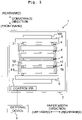
- the front side of a printer 1 is defined on the downstream side in a conveyance direction of recording paper 100, whereas the rear side of the printer 1 is defined on the upstream side in the conveyance direction.
- the left-right direction of the printer 1 is defined in such a direction along the paper width as is parallel to the conveyance plane of the recording paper 100 (the plane parallel to the page of Fig. 1 ) and is orthogonal to the conveyance direction.
- the left side of Fig. 1 is the left side of the printer 1
- the right side of Fig. 1 is the right side of the printer 1.
- the upper-lower or vertical direction of the printer 1 is defined in a direction orthogonal to the conveyance plane of the recording paper 100 (a direction orthogonal to the page of Fig. 1 ).
- the front side or near side is the upper side whereas the rear side or far side is the lower side.
- Those defined front, rear, left, right, upper, and lower will be used as appropriate in the following explanation.
- the printer 1 includes a case 2, a platen 3, four ink-jet heads 4, two conveyance rollers 5 and 6, and a controller 7.
- the platen 3 is placed horizontally in the case 2.
- the recording paper 100 is placed on the upper surface of the platen 3.
- the four ink-jet heads 4 are provided above the platen 3 to be juxtaposed in the front-rear direction.
- the two conveyance rollers 5 and 6 are arranged respectively on the rear side and the front side of the platen 3.
- the two conveyance rollers 5 and 6 are driven respectively by an undepicted motor to convey the recording paper 100 on the platen 3 to the front side.
- the controller 7 includes an FPGA (Field Programmable Gate Array), and the like. Illustration of the FPGA is omitted. Further, instead of the FPGA, a processor such as a CPU (Central Processing Unit) or the like may be used. Further, the controller 7 is connected with an external device 9 such as a PC or the like in a data communicable manner, to control each device of printer 1 based on print data sent from the external device 9.
- FPGA Field Programmable Gate Array
- an external device 9 such as a PC or the like in a data communicable manner, to control each device of printer 1 based on print data sent from the external device 9.
- the controller 7 controls the motor to drive the conveyance rollers 5 and 6 to cause the conveyance rollers 5 and 6 to convey the recording paper 100 in the conveyance direction, while controlling the ink-jet heads 4 to jet inks toward the recording paper 100. By virtue of this, image is printed on the recording paper 100.
- Head holders 8 are installed in the case 2.
- the head holders 8 are arranged above the platen 3 and juxtaposed between the conveyance rollers 5 and 6 in the front-rear direction.
- the head holders 8 hold the ink-jet heads 4 respectively.
- the four ink-jet heads 4 jet the inks of four colors: cyan (C), magenta (M), yellow (y), and black (K), respectively.
- Each of the ink-jet heads 4 is supplied with the ink of the corresponding color from an undepicted ink tank.
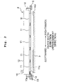
- each of the ink-jet heads 4 includes a holder 10 in a rectangular plate-like shape elongated in the paper width direction, and head units 11 attached to the holder 10. Nozzles 11a are formed in the lower surface of each of the head units 11.
- the holder 10 is provided with a slit 10a.
- a flexible substrate 51 connects the head units 11 and the controller 7, and the flexible substrate 51 is inserted through the slit 10a.
- the head units 11 are arranged to align in a staggered form along an arrangement direction and along the conveyance direction. Further, the head units 11 may be arranged obliquely, that is, along a direction intersecting the conveyance direction at an angle other than 90 degrees.
- a reservoir 12 is provided above the plurality of head units 11.
- An illustration of the reservoir 12 is omitted in Fig. 3 .
- the reservoir 12 is connected to one of the ink tanks (not depicted) via a tube 16 to temporarily retain the ink supplied from the ink tank.
- the reservoir 12 has a lower portion connected to the head units 11 to supply each of the head units 11 with the ink from the reservoir 12.
- Each of the head units 11 includes nozzles 11a and piezoelectric elements 11b.
- Each of the piezoelectric elements 11b is constructed of, for example, a piezoelectric body, and is driven by way of applying a voltage thereto.
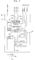
- the controller 7 includes an ink-jet head driving circuit 20 to drive the piezoelectric elements 11b of the head unit 11.
- Each of the piezoelectric elements 11b functions as a capacitor in the ink-jet head driving circuit 20.
- the ink-jet head driving circuit 20 includes a gate signal generation circuit 21, an amplifier 22, a CMOS (Complementary Metal-Oxide-Semiconductor) circuit 30, an impedance 25, and the like.
- the CMOS circuit 30 includes first PMOS (P-type Metal-Oxide-Semiconductor) transistor 31(1) to nth PMOS transistor 31(n) (n is an integer not less than two), and an NMOS (N-type Metal-Oxide-Semiconductor) transistor 32.
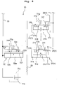
- the PMOS transistor 31 includes a grounded first P-type area 31a, an Nwell area 31b laid on the first P-type area 31a, a second P-type area 31c and a third P-type area 31d formed separate from each other in the Nwell area 31b, an oxide film 31e formed on the Nwell area 31b and positioned between the second P-type area 31c and the third P-type area 31d, a source terminal 31f and a drain terminal 31h formed of conductive bodies respectively on the second P-type area 31c and the third P-type area 31d, and a gate terminal 31g formed of a conductive body on the oxide film 31e.
- the NMOS transistor 32 includes a grounded P-type area 32a, a first N-type area 32b and a second N-type area 32c formed separate from each other in the P-type area 32a, an oxide film 32d formed on the P-type area 32a and positioned between the first N-type area 32b and the second N-type area 32c, a source terminal 32f and a drain terminal 32e formed of conductive bodies respectively on the first N-type area 32b and the second N-type area 32c, and a gate terminal 32g formed of a conductive body on the oxide film 32d.
- the ink-jet printer includes undepicted power sources different in voltage, that is, the first power source to the nth power source (n is an integer not less than two).
- the nth power source is, for example, a power source used for correction of non-jetting if ink is not jetted from a nozzle 11a.
- the first power source to the nth power source are connected respectively with the source terminals 31f of the first PMOS transistor 31(1) to the nth PMOS transistor 31(n) via a first power wire 24(1) to an nth power wire 24(n) (n is an integer not less than two).
- the first power wire 24(1) to the nth power wire 24(n) supply such voltages, that is, the voltages of the first power source to the nth power source, as VDD2-1 to VDD2-n, respectively.
- the magnitudes of the respective voltages are VDD2-1 ⁇ VDD2-2 ⁇ ... ⁇ VDD2-(n-1) ⁇ VDD2-n.
- the Nwell areas 31b of the first PMOS transistor 31(1) to the nth PMOS transistor 31(n) are all connected to the nth power wire 24(n).
- the difference in voltage between two successively numbered power sources is set in the range of a reference voltage difference such as, for example, from 0.5 to 1.0 [V].
- the difference between the voltage VDD2-n which is the highest voltage in the first power source to the nth power source and the next highest voltage VDD2-(n-1) to the highest voltage (the second highest voltage) is set in a range of a larger value than the reference voltage difference such as the range from 2.0 to 5.0 [V].
- the power source used for the correction of non-jetting is set at a higher voltage than the other voltages.
- the difference between the highest voltage and the second highest voltage is larger than the reference voltage difference between the predetermined applying voltage and another applying voltage.
- the gate terminal 31g of the PMOS transistor 31 and the gate terminal 32g of the NMOS transistor 32 are connected respectively with the amplifier 22.
- the drain terminal 31h of the PMOS transistor 31 and the drain terminal 32e of the NMOS transistor 32 are connected to each other, and connected to one end of the impedance 25.
- the wire 23 is at a voltage VSS1 or VSS2 such as at the ground potential.
- the source terminal 32f of the NMOS transistor 32 and the P-type area 32a are connected to the wire 23.
- the VSS2 is inputted to the source terminal 32f and the P-type area 32a from the wire 23.
- the wire 23 is connected to one side of the piezoelectric element 11b serving as the capacitor. The other side of the piezoelectric element 11b is connected to the other end of the impedance 25.
- the gate signal generation circuit 21 is connected to the wire 23 and the VSS1 is inputted thereto.
- the gate signal generation circuit 21 is connected with a first signal wire 21a, a second signal wire 21b, and a third signal wire 21c.
- Each of the first signal wire 21a, the second signal wire 21b and the third signal wire 21c has two signal wires.
- the first signal wire 21a is supplied with voltage from V1+ and V1-
- the second signal wire 21b is supplied with voltage from V2+ and V2-
- the third signal wire 21c is supplied with voltage from V3+ and V3-.
- V1+ and V1- correspond to the waveform signal (FIRE) for jetting the ink
- V2+ and V2- correspond to one signal (SIN) selected from the waveform signals adaptable to each ch
- V3+ and V3- correspond to a reference clock (CLK).
- the ink-jet head driving circuit 20 includes a voltage supply wire 26 to supply voltage VDD1.
- the gate signal generation circuit 21 is connected to the voltage supply wire 26 and the wire 23, uses the voltage VDD1 of the voltage supply wire 26 or VSS1 of the wire 23 and, based on the differential input, outputs an output signal "H” or "L".
- the amplifier 22 is connected to the gate terminal 32g of the NMOS transistor 32. Further, via a switch circuit 22a, the amplifier 22 is connected to the gate terminals 31g of the first PMOS transistor 31(1) to the nth PMOS transistor 31(n).
- the switch circuit 22a switches the connection to any of the gate terminals 31g of the PMOS transistors 31 based on, for example, a command from the FPGA.
- the amplifier 22 is connected to the wire 23, the voltage supply wire 26, and the nth power wire 24(n).
- the VSS1 and the VSS2 are inputted from the wire 23 to the amplifier 22.
- the output signal of the gate signal generation circuit 21 is inputted to the amplifier 22.
- the amplifier 22 uses the voltage VSS1 of the wire 23, the voltage VDD1 of the voltage supply wire 26, and the voltage VDD2-n of the nth power wire 24(n), to amplify the inputted signal and outputs the same to the gate terminal 32g of the NMOS transistor 32, and the gate terminal 31g of any of the first PMOS transistor 31(1) to the nth PMOS transistor 31(n). Further, the amplifier 22 is configured to suppress amplification of noise when amplifying the input signal.
- the piezoelectric element 11b is discharged.
- the piezoelectric element 11b is deformed to jet the ink from the nozzle 11a.
- the Nwell areas 31b of the first PMOS transistor 31(1) to the nth PMOS transistor 31(n) are all connected to the nth power wire 24(n). That is, among the voltages VDD2-1 to VDD2-n of the first power source to the nth power source, the highest voltage VDD2-n is applied to all of the Nwell areas 31b of the first PMOS transistor 31(1) to the nth PMOS transistor 31(n).
- the switch circuit 22a switches the connection to another PMOS transistor 31 than the nth PMOS transistor 31(n) such as the first PMOS transistor 31(1) for example, then the voltage VDD2-1 lower than the voltage of the piezoelectric element 11b (the voltage VDD2-n) is applied to the Nwell area 31b of the first PMOS transistor 31(1).
- the current flows reversely from the piezoelectric element 11b to the first PMOS transistor 31(1).
- the first PMOS transistor 31(1) is liable to destruction.
- the highest voltage VDD2-n is applied to all of the Nwell areas 31b of the first PMOS transistor 31(1) to the nth PMOS transistor 31(n).
- the highest voltage is equal to or higher than the voltage of the piezoelectric element 11b and, because the highest voltage is connected to all of the Nwell areas, the abovementioned current does not flow reversely. Thereby, it is possible to prevent destruction of the ink-jet head driving circuit 20.
- the common highest voltage is applied to all of the Nwell areas 31b of the PMOS transistors 31.
- the current is prevented from flowing reversely from the drain terminal 31h of the PMOS transistor 31 to the Nwell area 31b, with a simpler configuration than the case of providing high voltage power sources respectively for the PMOS transistors for preventing the reversed current.
- each PMOS transistor is provided with a power source to apply voltage equal to or higher than the VDD2-n, then another six power sources are needed (as with the number of PMOS transistors) for preventing the reversed current, in addition to the power sources (for example six power sources) to apply the voltages to the piezoelectric elements.
- the power sources for example six power sources
- the power source for applying the existing highest voltage is connected to all of the Nwell areas. Therefore, it is not necessary to provide other power sources for preventing the reversed current, and thus it is possible to realize reduction of the manufacturing cost and downsizing of the device.
- the voltage difference between the highest voltage and the second highest voltage is larger than the reference voltage difference
- the power source having the highest voltage for example, the power source for the correction of non-j etting
- the voltage difference between the power source for the correction of non-jetting and the other power sources is larger than the voltage difference between those other power sources.
- the power source for the correction of non-jetting is connected to the Nwell areas 31b so as to prevent the reversed current by utilizing the larger voltage difference.
- the ink-jet printer includes a dedicated power source (not depicted) for preventing the reversed current to apply voltage VDD2-(n+1) which is higher than the aforementioned highest voltage (VDD2-n).
- the dedicated power source is connected, via a (n+1)th power wire 24(n+1), with all of the Nwell areas 31b of the first PMOS transistor 31(1) to the nth PMOS transistor 31(n).
- the dedicated power source for preventing the reversed current is prepared to apply the voltage higher than the aforementioned highest voltage, and the dedicated power source is connected to each of the Nwell areas 31b of the PMOS transistors 31, it is possible to prevent the reversed current. That is, because of the voltage higher than the aforementioned highest voltage, it is possible to more reliably prevent the reversed current than the case of applying the highest voltage to the Nwell areas. Further, the dedicated power source is not used for driving of the piezoelectric elements. Therefore, it is possible to apply the stabilized voltage to each of the Nwell areas 31b.
- an embedded oxide film 32h is formed under the channel of the NMOS transistor 32. That is, the NMOS transistor 32 constructs an SOI (Silicon On Insulator) substrate.
- SOI Silicon On Insulator
- the SOI substrate by using the SOI substrate, even if there is a short distance between the wires, it is still possible to suppress production of parasitic capacitance, and damage is less likely to occur. Further, because it is possible to reduce the parasitic capacitance by using the SOI substrate, it is possible to realize high density layout, chip area miniaturization, operating speed-up, latch-up-free construction, and the like.
- a plurality of piezoelectric elements 11b may be provided for example as depicted in Fig. 9.
- Fig. 9 depicts such a case that another piezoelectric element 11b is connected between one end of the impedance 25, and the power wire 24(n+1) connected commonly to the Nwell areas 31b.
- the number of piezoelectric elements has increased to two, thereby improving the jetting property. By virtue of this, it is possible to reduce effects of crosstalk.
Landscapes
- Engineering & Computer Science (AREA)
- Microelectronics & Electronic Packaging (AREA)
- Particle Formation And Scattering Control In Inkjet Printers (AREA)
- Ink Jet (AREA)
Claims (9)
- Tintenstrahlkopfantriebsschaltung (30), umfassend für ein piezoelektrisches Element (11b) zum Ausstoßen von Tinte aus einer Düse (11a) und ein weiteres piezoelektrisches Element (11b) zum Ausstoßen von Tinte aus der Düse (11a), wobei das piezoelektrische Element (11b) eine Seite und eine andere Seite aufweist:PMOS-Transistoren (31), von denen jeder eine Nwell-Fläche (31b), einen Drain- (31h) und einen Source-Anschluss (31f) aufweist, wobei die jeweiligen Drain-Anschlüsse (31h) der PMOS-Transistoren (31) mit der anderen Seite des piezoelektrischen Elements (11b) zu verbinden sind; undeinen NMOS-Transistor (32), der einen Drain-Anschluss (32e) und einen Source-Anschluss (32f) aufweist, wobei der Drain-Anschluss (32e) des NMOS-Transistors (32) mit den jeweiligen Drain-Anschlüssen (31h) der PMOS-Transistoren (31) zu verbinden ist und der Source-Anschluss (32f) des NMOS-Transistors (32) mit der einen Seite des piezoelektrischen Elements (11b) zu verbinden ist, wobei:die jeweiligen Source-Anschlüsse (31f) der PMOS-Transistoren (31) mit jeweiligen Leistungsquellen verbunden sind,alle der Nwell-Flächen (31b) der PMOS-Transistoren (31) mit einer dedizierten Leistungsquelle verbunden sind,das weitere piezoelektrische Element zwischen die andere Seite des piezoelektrischen Elements (11b) und die dedizierte Leistungsquelle, die gemeinsam mit den Nwell-Flächen (31b) der PMOS-Transistoren (31) verbunden ist, zu verbinden ist, unddie Spannung der dedizierten Leistungsquelle, die mit den Nwell-Flächen (31b) aller der PMOS-Transistoren (31) verbunden ist, höher ist als die höchste Spannung der jeweiligen Leistungsquelle, die mit den jeweiligen Source-Anschlüssen (31f) der PMOS-Transistoren (31) verbunden sind.
- Tintenstrahlkopfantriebsschaltung nach Anspruch 1, wobei unter den Spannungen der jeweiligen Leistungsquellen und der dedizierten Leistungsquelle die Spannungsdifferenz zwischen der Spannung der dedizierten Leistungsquelle und der höchsten Spannung der jeweiligen Leistungsquellen größer ist als die Spannungsdifferenz zwischen der höchsten Spannung der jeweiligen Leistungsquellen und der Spannung der jeweiligen Leistungsquelle, die eine Stufe niedriger ist als die jeweilige Leistungsquelle mit der höchsten jeweiligen Spannung.
- Tintenstrahlkopfantriebsschaltung nach Anspruch 1 oder 2, wobei die dedizierte Leistungsquelle, die mit den Nwell-Flächen (31b) aller der PMOS-Transistoren (31) verbunden ist, nicht mit den Source-Anschlüssen (31f) der PMOS-Transistoren (31) verbunden ist.
- Tintenstrahlkopfantriebsschaltung nach einem der Ansprüche 1 bis 3, ferner umfassend einen Verstärker (22), der mit den PMOS-Transistoren (31), NMOS-Transistor (32) und der dedizierten Leistungsquelle verbunden ist, die mit den Nwell-Flächen (31b) aller der PMOS-Transistoren (31) verbunden ist.
- Tintenstrahlkopfantriebsschaltung nach Anspruch 4, wobei der Verstärker (22) eine Umschaltschaltung (22a) umfasst, die mit Gate-Anschlüssen (31g, 32g) der PMOS- und der NOMOS-Transistoren verbunden ist.
- Tintenstrahlkopfantriebsschaltung nach Anspruch 5, ferner umfassend eine Gate-Signalerzeugungsschaltung (21), die mit dem Verstärker (22) verbunden ist und dazu konfiguriert ist, in ein Differenzeingabesignal eingegeben zu werden.
- Tintenstrahlkopfantriebsschaltung nach einem der Ansprüche 1 bis 6, wobei der NMOS-Transistor (32) ein Silizium-auf-Isolator-Substrat bildet.
- Tintenstrahlkopfantriebsschaltung nach einem der Ansprüche 1 bis 7, wobei der Source-Anschluss (32f) des NMOS-Transistors (32) mit einem Draht (23) auf Erdungspotenzial verbunden ist.
- Tintenstrahldrucker, umfassend:die Tintenstrahlkopfantriebsschaltung (30) nach einem der Ansprüche 1 bis 8;eine Kopfeinheit (11), die das piezoelektrische Element (11b), das weitere piezoelektrische Element (11b) und die Düse (11a) beinhaltet, die dem piezoelektrischen Element (11b) und dem weiteren piezoelektrischen Element (11b) zugeordnet ist; unddie Leistungsquellen.
Applications Claiming Priority (2)
| Application Number | Priority Date | Filing Date | Title |
|---|---|---|---|
| JP2016073015A JP6816378B2 (ja) | 2016-03-31 | 2016-03-31 | インクジェットヘッド駆動回路 |
| EP17163388.6A EP3225397B1 (de) | 2016-03-31 | 2017-03-28 | Tintenstrahlkopfansteuerungsschaltung |
Related Parent Applications (2)
| Application Number | Title | Priority Date | Filing Date |
|---|---|---|---|
| EP17163388.6A Division EP3225397B1 (de) | 2016-03-31 | 2017-03-28 | Tintenstrahlkopfansteuerungsschaltung |
| EP17163388.6A Division-Into EP3225397B1 (de) | 2016-03-31 | 2017-03-28 | Tintenstrahlkopfansteuerungsschaltung |
Publications (2)
| Publication Number | Publication Date |
|---|---|
| EP3763530A1 EP3763530A1 (de) | 2021-01-13 |
| EP3763530B1 true EP3763530B1 (de) | 2022-11-23 |
Family
ID=58448478
Family Applications (2)
| Application Number | Title | Priority Date | Filing Date |
|---|---|---|---|
| EP20192542.7A Active EP3763530B1 (de) | 2016-03-31 | 2017-03-28 | Tintenstrahlkopfansteuerungsschaltung |
| EP17163388.6A Active EP3225397B1 (de) | 2016-03-31 | 2017-03-28 | Tintenstrahlkopfansteuerungsschaltung |
Family Applications After (1)
| Application Number | Title | Priority Date | Filing Date |
|---|---|---|---|
| EP17163388.6A Active EP3225397B1 (de) | 2016-03-31 | 2017-03-28 | Tintenstrahlkopfansteuerungsschaltung |
Country Status (4)
| Country | Link |
|---|---|
| US (2) | US10315416B2 (de) |
| EP (2) | EP3763530B1 (de) |
| JP (1) | JP6816378B2 (de) |
| CN (1) | CN107336521B (de) |
Families Citing this family (5)
| Publication number | Priority date | Publication date | Assignee | Title |
|---|---|---|---|---|
| JP7069761B2 (ja) * | 2018-01-31 | 2022-05-18 | セイコーエプソン株式会社 | 液体吐出装置 |
| JP6973247B2 (ja) * | 2018-03-30 | 2021-11-24 | ブラザー工業株式会社 | 電源基板及び印刷装置 |
| TWI696755B (zh) * | 2019-01-24 | 2020-06-21 | 研能科技股份有限公司 | 微機電泵模組 |
| JP7275924B2 (ja) * | 2019-06-28 | 2023-05-18 | セイコーエプソン株式会社 | 液体吐出装置、駆動回路、及び集積回路 |
| JP2023031951A (ja) * | 2021-08-26 | 2023-03-09 | ブラザー工業株式会社 | 画像形成方法、及び画像形成装置 |
Family Cites Families (17)
| Publication number | Priority date | Publication date | Assignee | Title |
|---|---|---|---|---|
| US4385947A (en) * | 1981-07-29 | 1983-05-31 | Harris Corporation | Method for fabricating CMOS in P substrate with single guard ring using local oxidation |
| JP3641511B2 (ja) * | 1995-06-16 | 2005-04-20 | 株式会社ルネサステクノロジ | 半導体装置 |
| JPH11129480A (ja) * | 1997-10-31 | 1999-05-18 | Canon Inc | 記録ヘッド及び該記録ヘッドを用いた記録装置 |
| JP2002094364A (ja) * | 2000-09-19 | 2002-03-29 | Toshiba Tec Corp | 容量性素子の駆動方法及び駆動装置 |
| US6664608B1 (en) * | 2001-11-30 | 2003-12-16 | Sun Microsystems, Inc. | Back-biased MOS device |
| JP2004050492A (ja) | 2002-07-17 | 2004-02-19 | Sharp Corp | インクジェットヘッド駆動回路 |
| JP2004153411A (ja) * | 2002-10-29 | 2004-05-27 | Sharp Corp | 多値出力半導体装置,インクジェット記録装置 |
| JP2006059910A (ja) * | 2004-08-18 | 2006-03-02 | Fujitsu Ltd | 半導体装置 |
| JP4604610B2 (ja) * | 2004-09-01 | 2011-01-05 | 富士ゼロックス株式会社 | インクジェット記録ヘッドの駆動波形生成回路及びインクジェット記録装置 |
| JP2007098795A (ja) * | 2005-10-05 | 2007-04-19 | Fuji Xerox Co Ltd | 容量性負荷の駆動回路及び方法並びに液滴吐出装置 |
| US8427115B2 (en) * | 2008-07-08 | 2013-04-23 | Toshiba Tec Kabushiki Kaisha | Driving device for capacitance type actuator and driving device for ink jet head |
| JP5909049B2 (ja) * | 2011-03-31 | 2016-04-26 | キヤノン株式会社 | 液体吐出ヘッドおよび液体吐出装置 |
| JP2013010227A (ja) * | 2011-06-29 | 2013-01-17 | Konica Minolta Ij Technologies Inc | インクジェットヘッドの駆動回路及びインクジェットヘッド |
| JP2014087169A (ja) * | 2012-10-24 | 2014-05-12 | Seiko Epson Corp | 駆動装置、駆動回路、ロボットハンド、ロボット、電子部品搬送装置、電子部品検査装置、送液ポンプ、印刷装置、電子時計、投影装置 |
| JP6127814B2 (ja) * | 2013-07-31 | 2017-05-17 | ブラザー工業株式会社 | 液体吐出装置 |
| JP6369057B2 (ja) * | 2014-03-05 | 2018-08-08 | セイコーエプソン株式会社 | 半導体装置、液体吐出ヘッド、及び液体吐出装置 |
| JP6455264B2 (ja) * | 2015-03-20 | 2019-01-23 | セイコーエプソン株式会社 | 液体吐出装置、駆動回路およびヘッドユニット |
-
2016
- 2016-03-31 JP JP2016073015A patent/JP6816378B2/ja active Active
-
2017
- 2017-03-22 CN CN201710173224.6A patent/CN107336521B/zh active Active
- 2017-03-27 US US15/469,927 patent/US10315416B2/en active Active
- 2017-03-28 EP EP20192542.7A patent/EP3763530B1/de active Active
- 2017-03-28 EP EP17163388.6A patent/EP3225397B1/de active Active
-
2019
- 2019-04-29 US US16/397,527 patent/US10933631B2/en active Active
Also Published As
| Publication number | Publication date |
|---|---|
| EP3763530A1 (de) | 2021-01-13 |
| US20190255838A1 (en) | 2019-08-22 |
| US10933631B2 (en) | 2021-03-02 |
| JP2017177756A (ja) | 2017-10-05 |
| CN107336521B (zh) | 2019-10-25 |
| EP3225397B1 (de) | 2020-10-21 |
| JP6816378B2 (ja) | 2021-01-20 |
| CN107336521A (zh) | 2017-11-10 |
| US10315416B2 (en) | 2019-06-11 |
| US20170282537A1 (en) | 2017-10-05 |
| EP3225397A1 (de) | 2017-10-04 |
Similar Documents
| Publication | Publication Date | Title |
|---|---|---|
| US10933631B2 (en) | Ink-jet head driving circuit and ink-jet printer with ink-jet head driving circuit | |
| US7887149B2 (en) | Capacitive load driving circuit and image forming device | |
| US10870272B2 (en) | Liquid discharging apparatus and driving circuit board | |
| CN111204134B (zh) | 驱动电路、液体喷出装置以及驱动方法 | |
| US10315415B2 (en) | Printhead and printing apparatus | |
| JP5163207B2 (ja) | 液体噴射装置、及び印刷装置 | |
| JP5063314B2 (ja) | 素子基板、記録ヘッド、ヘッドカートリッジ及び記録装置 | |
| US10391788B2 (en) | Element substrate, printhead, and printing apparatus | |
| US9340022B1 (en) | Liquid discharging substrate, printhead, and printing apparatus | |
| US12565040B2 (en) | Head substrate, liquid discharging head, and liquid discharging device | |
| JP5663435B2 (ja) | 液体吐出装置およびその制御方法 | |
| US9365036B2 (en) | Printing apparatus and printhead | |
| JP5572601B2 (ja) | 液体吐出装置 | |
| JP5440684B2 (ja) | 駆動回路 | |
| US20260056064A1 (en) | Temperature detecting circuit, temperature detecting method, and circuit board | |
| CN110315845A (zh) | 电源基板及打印装置 | |
| CN117799324A (zh) | 驱动电路单元、头单元以及液体喷出装置 | |
| CN117799323A (zh) | 驱动单元、液体喷出头单元以及液体喷出装置 | |
| US9522529B2 (en) | Substrate for liquid ejection head, liquid ejection head, and apparatus and method for ejecting liquid | |
| CN117799326A (zh) | 第一驱动单元、第一液体喷出头单元以及液体喷出装置 | |
| CN117799318A (zh) | 驱动单元、液体喷出头单元以及液体喷出装置 | |
| CN117799308A (zh) | 液体喷出装置及冷却单元 |
Legal Events
| Date | Code | Title | Description |
|---|---|---|---|
| PUAI | Public reference made under article 153(3) epc to a published international application that has entered the european phase |
Free format text: ORIGINAL CODE: 0009012 |
|
| STAA | Information on the status of an ep patent application or granted ep patent |
Free format text: STATUS: THE APPLICATION HAS BEEN PUBLISHED |
|
| AC | Divisional application: reference to earlier application |
Ref document number: 3225397 Country of ref document: EP Kind code of ref document: P |
|
| AK | Designated contracting states |
Kind code of ref document: A1 Designated state(s): AL AT BE BG CH CY CZ DE DK EE ES FI FR GB GR HR HU IE IS IT LI LT LU LV MC MK MT NL NO PL PT RO RS SE SI SK SM TR |
|
| STAA | Information on the status of an ep patent application or granted ep patent |
Free format text: STATUS: REQUEST FOR EXAMINATION WAS MADE |
|
| 17P | Request for examination filed |
Effective date: 20210709 |
|
| RBV | Designated contracting states (corrected) |
Designated state(s): AL AT BE BG CH CY CZ DE DK EE ES FI FR GB GR HR HU IE IS IT LI LT LU LV MC MK MT NL NO PL PT RO RS SE SI SK SM TR |
|
| GRAP | Despatch of communication of intention to grant a patent |
Free format text: ORIGINAL CODE: EPIDOSNIGR1 |
|
| STAA | Information on the status of an ep patent application or granted ep patent |
Free format text: STATUS: GRANT OF PATENT IS INTENDED |
|
| INTG | Intention to grant announced |
Effective date: 20220829 |
|
| GRAS | Grant fee paid |
Free format text: ORIGINAL CODE: EPIDOSNIGR3 |
|
| GRAA | (expected) grant |
Free format text: ORIGINAL CODE: 0009210 |
|
| STAA | Information on the status of an ep patent application or granted ep patent |
Free format text: STATUS: THE PATENT HAS BEEN GRANTED |
|
| AC | Divisional application: reference to earlier application |
Ref document number: 3225397 Country of ref document: EP Kind code of ref document: P |
|
| AK | Designated contracting states |
Kind code of ref document: B1 Designated state(s): AL AT BE BG CH CY CZ DE DK EE ES FI FR GB GR HR HU IE IS IT LI LT LU LV MC MK MT NL NO PL PT RO RS SE SI SK SM TR |
|
| REG | Reference to a national code |
Ref country code: GB Ref legal event code: FG4D |
|
| REG | Reference to a national code |
Ref country code: CH Ref legal event code: EP |
|
| REG | Reference to a national code |
Ref country code: AT Ref legal event code: REF Ref document number: 1532904 Country of ref document: AT Kind code of ref document: T Effective date: 20221215 Ref country code: DE Ref legal event code: R096 Ref document number: 602017064060 Country of ref document: DE |
|
| REG | Reference to a national code |
Ref country code: IE Ref legal event code: FG4D |
|
| REG | Reference to a national code |
Ref country code: LT Ref legal event code: MG9D |
|
| REG | Reference to a national code |
Ref country code: NL Ref legal event code: MP Effective date: 20221123 |
|
| REG | Reference to a national code |
Ref country code: AT Ref legal event code: MK05 Ref document number: 1532904 Country of ref document: AT Kind code of ref document: T Effective date: 20221123 |
|
| PG25 | Lapsed in a contracting state [announced via postgrant information from national office to epo] |
Ref country code: SE Free format text: LAPSE BECAUSE OF FAILURE TO SUBMIT A TRANSLATION OF THE DESCRIPTION OR TO PAY THE FEE WITHIN THE PRESCRIBED TIME-LIMIT Effective date: 20221123 Ref country code: PT Free format text: LAPSE BECAUSE OF FAILURE TO SUBMIT A TRANSLATION OF THE DESCRIPTION OR TO PAY THE FEE WITHIN THE PRESCRIBED TIME-LIMIT Effective date: 20230323 Ref country code: NO Free format text: LAPSE BECAUSE OF FAILURE TO SUBMIT A TRANSLATION OF THE DESCRIPTION OR TO PAY THE FEE WITHIN THE PRESCRIBED TIME-LIMIT Effective date: 20230223 Ref country code: LT Free format text: LAPSE BECAUSE OF FAILURE TO SUBMIT A TRANSLATION OF THE DESCRIPTION OR TO PAY THE FEE WITHIN THE PRESCRIBED TIME-LIMIT Effective date: 20221123 Ref country code: FI Free format text: LAPSE BECAUSE OF FAILURE TO SUBMIT A TRANSLATION OF THE DESCRIPTION OR TO PAY THE FEE WITHIN THE PRESCRIBED TIME-LIMIT Effective date: 20221123 Ref country code: ES Free format text: LAPSE BECAUSE OF FAILURE TO SUBMIT A TRANSLATION OF THE DESCRIPTION OR TO PAY THE FEE WITHIN THE PRESCRIBED TIME-LIMIT Effective date: 20221123 Ref country code: AT Free format text: LAPSE BECAUSE OF FAILURE TO SUBMIT A TRANSLATION OF THE DESCRIPTION OR TO PAY THE FEE WITHIN THE PRESCRIBED TIME-LIMIT Effective date: 20221123 |
|
| PG25 | Lapsed in a contracting state [announced via postgrant information from national office to epo] |
Ref country code: RS Free format text: LAPSE BECAUSE OF FAILURE TO SUBMIT A TRANSLATION OF THE DESCRIPTION OR TO PAY THE FEE WITHIN THE PRESCRIBED TIME-LIMIT Effective date: 20221123 Ref country code: PL Free format text: LAPSE BECAUSE OF FAILURE TO SUBMIT A TRANSLATION OF THE DESCRIPTION OR TO PAY THE FEE WITHIN THE PRESCRIBED TIME-LIMIT Effective date: 20221123 Ref country code: LV Free format text: LAPSE BECAUSE OF FAILURE TO SUBMIT A TRANSLATION OF THE DESCRIPTION OR TO PAY THE FEE WITHIN THE PRESCRIBED TIME-LIMIT Effective date: 20221123 Ref country code: IS Free format text: LAPSE BECAUSE OF FAILURE TO SUBMIT A TRANSLATION OF THE DESCRIPTION OR TO PAY THE FEE WITHIN THE PRESCRIBED TIME-LIMIT Effective date: 20230323 Ref country code: HR Free format text: LAPSE BECAUSE OF FAILURE TO SUBMIT A TRANSLATION OF THE DESCRIPTION OR TO PAY THE FEE WITHIN THE PRESCRIBED TIME-LIMIT Effective date: 20221123 Ref country code: GR Free format text: LAPSE BECAUSE OF FAILURE TO SUBMIT A TRANSLATION OF THE DESCRIPTION OR TO PAY THE FEE WITHIN THE PRESCRIBED TIME-LIMIT Effective date: 20230224 |
|
| PG25 | Lapsed in a contracting state [announced via postgrant information from national office to epo] |
Ref country code: NL Free format text: LAPSE BECAUSE OF FAILURE TO SUBMIT A TRANSLATION OF THE DESCRIPTION OR TO PAY THE FEE WITHIN THE PRESCRIBED TIME-LIMIT Effective date: 20221123 |
|
| P01 | Opt-out of the competence of the unified patent court (upc) registered |
Effective date: 20230529 |
|
| PG25 | Lapsed in a contracting state [announced via postgrant information from national office to epo] |
Ref country code: SM Free format text: LAPSE BECAUSE OF FAILURE TO SUBMIT A TRANSLATION OF THE DESCRIPTION OR TO PAY THE FEE WITHIN THE PRESCRIBED TIME-LIMIT Effective date: 20221123 Ref country code: RO Free format text: LAPSE BECAUSE OF FAILURE TO SUBMIT A TRANSLATION OF THE DESCRIPTION OR TO PAY THE FEE WITHIN THE PRESCRIBED TIME-LIMIT Effective date: 20221123 Ref country code: EE Free format text: LAPSE BECAUSE OF FAILURE TO SUBMIT A TRANSLATION OF THE DESCRIPTION OR TO PAY THE FEE WITHIN THE PRESCRIBED TIME-LIMIT Effective date: 20221123 Ref country code: DK Free format text: LAPSE BECAUSE OF FAILURE TO SUBMIT A TRANSLATION OF THE DESCRIPTION OR TO PAY THE FEE WITHIN THE PRESCRIBED TIME-LIMIT Effective date: 20221123 Ref country code: CZ Free format text: LAPSE BECAUSE OF FAILURE TO SUBMIT A TRANSLATION OF THE DESCRIPTION OR TO PAY THE FEE WITHIN THE PRESCRIBED TIME-LIMIT Effective date: 20221123 |
|
| REG | Reference to a national code |
Ref country code: DE Ref legal event code: R097 Ref document number: 602017064060 Country of ref document: DE |
|
| PG25 | Lapsed in a contracting state [announced via postgrant information from national office to epo] |
Ref country code: SK Free format text: LAPSE BECAUSE OF FAILURE TO SUBMIT A TRANSLATION OF THE DESCRIPTION OR TO PAY THE FEE WITHIN THE PRESCRIBED TIME-LIMIT Effective date: 20221123 Ref country code: AL Free format text: LAPSE BECAUSE OF FAILURE TO SUBMIT A TRANSLATION OF THE DESCRIPTION OR TO PAY THE FEE WITHIN THE PRESCRIBED TIME-LIMIT Effective date: 20221123 |
|
| PLBE | No opposition filed within time limit |
Free format text: ORIGINAL CODE: 0009261 |
|
| STAA | Information on the status of an ep patent application or granted ep patent |
Free format text: STATUS: NO OPPOSITION FILED WITHIN TIME LIMIT |
|
| PG25 | Lapsed in a contracting state [announced via postgrant information from national office to epo] |
Ref country code: MC Free format text: LAPSE BECAUSE OF FAILURE TO SUBMIT A TRANSLATION OF THE DESCRIPTION OR TO PAY THE FEE WITHIN THE PRESCRIBED TIME-LIMIT Effective date: 20221123 |
|
| REG | Reference to a national code |
Ref country code: CH Ref legal event code: PL |
|
| 26N | No opposition filed |
Effective date: 20230824 |
|
| PG25 | Lapsed in a contracting state [announced via postgrant information from national office to epo] |
Ref country code: SI Free format text: LAPSE BECAUSE OF FAILURE TO SUBMIT A TRANSLATION OF THE DESCRIPTION OR TO PAY THE FEE WITHIN THE PRESCRIBED TIME-LIMIT Effective date: 20221123 |
|
| REG | Reference to a national code |
Ref country code: BE Ref legal event code: MM Effective date: 20230331 |
|
| PG25 | Lapsed in a contracting state [announced via postgrant information from national office to epo] |
Ref country code: LU Free format text: LAPSE BECAUSE OF NON-PAYMENT OF DUE FEES Effective date: 20230328 |
|
| REG | Reference to a national code |
Ref country code: IE Ref legal event code: MM4A |
|
| PG25 | Lapsed in a contracting state [announced via postgrant information from national office to epo] |
Ref country code: LI Free format text: LAPSE BECAUSE OF NON-PAYMENT OF DUE FEES Effective date: 20230331 Ref country code: IE Free format text: LAPSE BECAUSE OF NON-PAYMENT OF DUE FEES Effective date: 20230328 Ref country code: CH Free format text: LAPSE BECAUSE OF NON-PAYMENT OF DUE FEES Effective date: 20230331 |
|
| PG25 | Lapsed in a contracting state [announced via postgrant information from national office to epo] |
Ref country code: BE Free format text: LAPSE BECAUSE OF NON-PAYMENT OF DUE FEES Effective date: 20230331 |
|
| PG25 | Lapsed in a contracting state [announced via postgrant information from national office to epo] |
Ref country code: IT Free format text: LAPSE BECAUSE OF FAILURE TO SUBMIT A TRANSLATION OF THE DESCRIPTION OR TO PAY THE FEE WITHIN THE PRESCRIBED TIME-LIMIT Effective date: 20221123 |
|
| PG25 | Lapsed in a contracting state [announced via postgrant information from national office to epo] |
Ref country code: BG Free format text: LAPSE BECAUSE OF FAILURE TO SUBMIT A TRANSLATION OF THE DESCRIPTION OR TO PAY THE FEE WITHIN THE PRESCRIBED TIME-LIMIT Effective date: 20221123 |
|
| PG25 | Lapsed in a contracting state [announced via postgrant information from national office to epo] |
Ref country code: BG Free format text: LAPSE BECAUSE OF FAILURE TO SUBMIT A TRANSLATION OF THE DESCRIPTION OR TO PAY THE FEE WITHIN THE PRESCRIBED TIME-LIMIT Effective date: 20221123 |
|
| PG25 | Lapsed in a contracting state [announced via postgrant information from national office to epo] |
Ref country code: CY Free format text: LAPSE BECAUSE OF FAILURE TO SUBMIT A TRANSLATION OF THE DESCRIPTION OR TO PAY THE FEE WITHIN THE PRESCRIBED TIME-LIMIT; INVALID AB INITIO Effective date: 20170328 |
|
| PG25 | Lapsed in a contracting state [announced via postgrant information from national office to epo] |
Ref country code: HU Free format text: LAPSE BECAUSE OF FAILURE TO SUBMIT A TRANSLATION OF THE DESCRIPTION OR TO PAY THE FEE WITHIN THE PRESCRIBED TIME-LIMIT; INVALID AB INITIO Effective date: 20170328 |
|
| PG25 | Lapsed in a contracting state [announced via postgrant information from national office to epo] |
Ref country code: TR Free format text: LAPSE BECAUSE OF FAILURE TO SUBMIT A TRANSLATION OF THE DESCRIPTION OR TO PAY THE FEE WITHIN THE PRESCRIBED TIME-LIMIT Effective date: 20221123 |
|
| PGFP | Annual fee paid to national office [announced via postgrant information from national office to epo] |
Ref country code: GB Payment date: 20260211 Year of fee payment: 10 |
|
| PGFP | Annual fee paid to national office [announced via postgrant information from national office to epo] |
Ref country code: DE Payment date: 20260213 Year of fee payment: 10 |
|
| PGFP | Annual fee paid to national office [announced via postgrant information from national office to epo] |
Ref country code: FR Payment date: 20260209 Year of fee payment: 10 |