EP3756262B1 - Multi-voltage charging apparatus - Google Patents
Multi-voltage charging apparatus Download PDFInfo
- Publication number
- EP3756262B1 EP3756262B1 EP18906778.8A EP18906778A EP3756262B1 EP 3756262 B1 EP3756262 B1 EP 3756262B1 EP 18906778 A EP18906778 A EP 18906778A EP 3756262 B1 EP3756262 B1 EP 3756262B1
- Authority
- EP
- European Patent Office
- Prior art keywords
- voltage
- terminal
- transistor switch
- charging
- coupled
- Prior art date
- Legal status (The legal status is an assumption and is not a legal conclusion. Google has not performed a legal analysis and makes no representation as to the accuracy of the status listed.)
- Active
Links
Images


Classifications
-
- H—ELECTRICITY
- H02—GENERATION; CONVERSION OR DISTRIBUTION OF ELECTRIC POWER
- H02J—ELECTRIC POWER NETWORKS; CIRCUIT ARRANGEMENTS OR SYSTEMS FOR SUPPLYING OR DISTRIBUTING ELECTRIC POWER; SYSTEMS FOR STORING ELECTRIC ENERGY
- H02J1/00—Circuit arrangements for DC mains or DC distribution networks
- H02J1/10—Parallel operation of DC sources
- H02J1/122—Provisions for temporary connection of DC sources of essentially the same voltage, e.g. jumpstart cables
-
- B—PERFORMING OPERATIONS; TRANSPORTING
- B60—VEHICLES IN GENERAL
- B60L—PROPULSION OF ELECTRICALLY-PROPELLED VEHICLES; SUPPLYING ELECTRIC POWER FOR AUXILIARY EQUIPMENT OF ELECTRICALLY-PROPELLED VEHICLES; ELECTRODYNAMIC BRAKE SYSTEMS FOR VEHICLES IN GENERAL; MAGNETIC SUSPENSION OR LEVITATION FOR VEHICLES; MONITORING OPERATING VARIABLES OF ELECTRICALLY-PROPELLED VEHICLES; ELECTRIC SAFETY DEVICES FOR ELECTRICALLY-PROPELLED VEHICLES
- B60L53/00—Methods of charging batteries, specially adapted for electric vehicles; Charging stations or on-board charging equipment therefor; Exchange of energy storage elements in electric vehicles
- B60L53/30—Constructional details of charging stations
-
- B—PERFORMING OPERATIONS; TRANSPORTING
- B60—VEHICLES IN GENERAL
- B60L—PROPULSION OF ELECTRICALLY-PROPELLED VEHICLES; SUPPLYING ELECTRIC POWER FOR AUXILIARY EQUIPMENT OF ELECTRICALLY-PROPELLED VEHICLES; ELECTRODYNAMIC BRAKE SYSTEMS FOR VEHICLES IN GENERAL; MAGNETIC SUSPENSION OR LEVITATION FOR VEHICLES; MONITORING OPERATING VARIABLES OF ELECTRICALLY-PROPELLED VEHICLES; ELECTRIC SAFETY DEVICES FOR ELECTRICALLY-PROPELLED VEHICLES
- B60L53/00—Methods of charging batteries, specially adapted for electric vehicles; Charging stations or on-board charging equipment therefor; Exchange of energy storage elements in electric vehicles
- B60L53/50—Charging stations characterised by energy-storage or power-generation means
- B60L53/53—Batteries
-
- B—PERFORMING OPERATIONS; TRANSPORTING
- B60—VEHICLES IN GENERAL
- B60R—VEHICLES, VEHICLE FITTINGS, OR VEHICLE PARTS, NOT OTHERWISE PROVIDED FOR
- B60R16/00—Electric or fluid circuits specially adapted for vehicles and not otherwise provided for; Arrangement of elements of electric or fluid circuits specially adapted for vehicles and not otherwise provided for
- B60R16/02—Electric or fluid circuits specially adapted for vehicles and not otherwise provided for; Arrangement of elements of electric or fluid circuits specially adapted for vehicles and not otherwise provided for electric constitutive elements
- B60R16/03—Electric or fluid circuits specially adapted for vehicles and not otherwise provided for; Arrangement of elements of electric or fluid circuits specially adapted for vehicles and not otherwise provided for electric constitutive elements for supply of electrical power to vehicle subsystems or for
- B60R16/033—Electric or fluid circuits specially adapted for vehicles and not otherwise provided for; Arrangement of elements of electric or fluid circuits specially adapted for vehicles and not otherwise provided for electric constitutive elements for supply of electrical power to vehicle subsystems or for characterised by the use of electrical cells or batteries
-
- E—FIXED CONSTRUCTIONS
- E05—LOCKS; KEYS; WINDOW OR DOOR FITTINGS; SAFES
- E05B—LOCKS; ACCESSORIES THEREFOR; HANDCUFFS
- E05B47/00—Operating or controlling locks or other fastening devices by electric or magnetic means
- E05B47/02—Movement of the bolt by electromagnetic means; Adaptation of locks, latches, or parts thereof, for movement of the bolt by electromagnetic means
- E05B47/023—Movement of the bolt by electromagnetic means; Adaptation of locks, latches, or parts thereof, for movement of the bolt by electromagnetic means the bolt moving pivotally or rotatively
-
- H—ELECTRICITY
- H02—GENERATION; CONVERSION OR DISTRIBUTION OF ELECTRIC POWER
- H02J—ELECTRIC POWER NETWORKS; CIRCUIT ARRANGEMENTS OR SYSTEMS FOR SUPPLYING OR DISTRIBUTING ELECTRIC POWER; SYSTEMS FOR STORING ELECTRIC ENERGY
- H02J1/00—Circuit arrangements for DC mains or DC distribution networks
- H02J1/08—Three-wire DC power distribution systems; Systems having more than three wires
- H02J1/082—DC supplies with two or more different DC voltage levels
-
- H—ELECTRICITY
- H02—GENERATION; CONVERSION OR DISTRIBUTION OF ELECTRIC POWER
- H02J—ELECTRIC POWER NETWORKS; CIRCUIT ARRANGEMENTS OR SYSTEMS FOR SUPPLYING OR DISTRIBUTING ELECTRIC POWER; SYSTEMS FOR STORING ELECTRIC ENERGY
- H02J7/00—Circuit arrangements for charging or discharging batteries or for supplying loads from batteries
- H02J7/34—Parallel operation in networks using both storage and other DC sources, e.g. providing buffering
- H02J7/342—The other DC source being a battery actively interacting with the first one, i.e. battery to battery charging
-
- H—ELECTRICITY
- H02—GENERATION; CONVERSION OR DISTRIBUTION OF ELECTRIC POWER
- H02J—ELECTRIC POWER NETWORKS; CIRCUIT ARRANGEMENTS OR SYSTEMS FOR SUPPLYING OR DISTRIBUTING ELECTRIC POWER; SYSTEMS FOR STORING ELECTRIC ENERGY
- H02J7/00—Circuit arrangements for charging or discharging batteries or for supplying loads from batteries
- H02J7/485—Circuit arrangements for charging or discharging batteries or for supplying loads from batteries with provisions for charging different types of batteries
-
- H—ELECTRICITY
- H02—GENERATION; CONVERSION OR DISTRIBUTION OF ELECTRIC POWER
- H02J—ELECTRIC POWER NETWORKS; CIRCUIT ARRANGEMENTS OR SYSTEMS FOR SUPPLYING OR DISTRIBUTING ELECTRIC POWER; SYSTEMS FOR STORING ELECTRIC ENERGY
- H02J7/00—Circuit arrangements for charging or discharging batteries or for supplying loads from batteries
- H02J7/60—Circuit arrangements for charging or discharging batteries or for supplying loads from batteries including safety or protection arrangements
- H02J7/663—Circuit arrangements for charging or discharging batteries or for supplying loads from batteries including safety or protection arrangements using battery or load disconnect circuits
-
- H—ELECTRICITY
- H02—GENERATION; CONVERSION OR DISTRIBUTION OF ELECTRIC POWER
- H02J—ELECTRIC POWER NETWORKS; CIRCUIT ARRANGEMENTS OR SYSTEMS FOR SUPPLYING OR DISTRIBUTING ELECTRIC POWER; SYSTEMS FOR STORING ELECTRIC ENERGY
- H02J7/00—Circuit arrangements for charging or discharging batteries or for supplying loads from batteries
- H02J7/60—Circuit arrangements for charging or discharging batteries or for supplying loads from batteries including safety or protection arrangements
- H02J7/68—Circuit arrangements for charging or discharging batteries or for supplying loads from batteries including safety or protection arrangements using circuits for correcting or protecting against reverse-polarity
-
- H—ELECTRICITY
- H02—GENERATION; CONVERSION OR DISTRIBUTION OF ELECTRIC POWER
- H02J—ELECTRIC POWER NETWORKS; CIRCUIT ARRANGEMENTS OR SYSTEMS FOR SUPPLYING OR DISTRIBUTING ELECTRIC POWER; SYSTEMS FOR STORING ELECTRIC ENERGY
- H02J7/00—Circuit arrangements for charging or discharging batteries or for supplying loads from batteries
- H02J7/70—Circuit arrangements for charging or discharging batteries or for supplying loads from batteries characterised by the mechanical construction
-
- H—ELECTRICITY
- H02—GENERATION; CONVERSION OR DISTRIBUTION OF ELECTRIC POWER
- H02J—ELECTRIC POWER NETWORKS; CIRCUIT ARRANGEMENTS OR SYSTEMS FOR SUPPLYING OR DISTRIBUTING ELECTRIC POWER; SYSTEMS FOR STORING ELECTRIC ENERGY
- H02J7/00—Circuit arrangements for charging or discharging batteries or for supplying loads from batteries
- H02J7/90—Regulation of charging or discharging current or voltage
- H02J7/96—Regulation of charging or discharging current or voltage in response to battery voltage
-
- H—ELECTRICITY
- H01—ELECTRIC ELEMENTS
- H01M—PROCESSES OR MEANS, e.g. BATTERIES, FOR THE DIRECT CONVERSION OF CHEMICAL ENERGY INTO ELECTRICAL ENERGY
- H01M10/00—Secondary cells; Manufacture thereof
- H01M10/42—Methods or arrangements for servicing or maintenance of secondary cells or secondary half-cells
- H01M10/44—Methods for charging or discharging
- H01M10/441—Methods for charging or discharging for several batteries or cells simultaneously or sequentially
-
- H—ELECTRICITY
- H01—ELECTRIC ELEMENTS
- H01M—PROCESSES OR MEANS, e.g. BATTERIES, FOR THE DIRECT CONVERSION OF CHEMICAL ENERGY INTO ELECTRICAL ENERGY
- H01M2220/00—Batteries for particular applications
- H01M2220/20—Batteries in motive systems, e.g. vehicle, ship, plane
-
- H—ELECTRICITY
- H02—GENERATION; CONVERSION OR DISTRIBUTION OF ELECTRIC POWER
- H02J—ELECTRIC POWER NETWORKS; CIRCUIT ARRANGEMENTS OR SYSTEMS FOR SUPPLYING OR DISTRIBUTING ELECTRIC POWER; SYSTEMS FOR STORING ELECTRIC ENERGY
- H02J2105/00—Networks for supplying or distributing electric power characterised by their spatial reach or by the load
- H02J2105/30—Networks for supplying or distributing electric power characterised by their spatial reach or by the load the load networks being external to vehicles, i.e. exchanging power with vehicles
- H02J2105/33—Networks for supplying or distributing electric power characterised by their spatial reach or by the load the load networks being external to vehicles, i.e. exchanging power with vehicles exchanging power with road vehicles
-
- H—ELECTRICITY
- H02—GENERATION; CONVERSION OR DISTRIBUTION OF ELECTRIC POWER
- H02J—ELECTRIC POWER NETWORKS; CIRCUIT ARRANGEMENTS OR SYSTEMS FOR SUPPLYING OR DISTRIBUTING ELECTRIC POWER; SYSTEMS FOR STORING ELECTRIC ENERGY
- H02J7/00—Circuit arrangements for charging or discharging batteries or for supplying loads from batteries
- H02J7/60—Circuit arrangements for charging or discharging batteries or for supplying loads from batteries including safety or protection arrangements
- H02J7/62—Circuit arrangements for charging or discharging batteries or for supplying loads from batteries including safety or protection arrangements against overcurrent
-
- Y—GENERAL TAGGING OF NEW TECHNOLOGICAL DEVELOPMENTS; GENERAL TAGGING OF CROSS-SECTIONAL TECHNOLOGIES SPANNING OVER SEVERAL SECTIONS OF THE IPC; TECHNICAL SUBJECTS COVERED BY FORMER USPC CROSS-REFERENCE ART COLLECTIONS [XRACs] AND DIGESTS
- Y02—TECHNOLOGIES OR APPLICATIONS FOR MITIGATION OR ADAPTATION AGAINST CLIMATE CHANGE
- Y02E—REDUCTION OF GREENHOUSE GAS [GHG] EMISSIONS, RELATED TO ENERGY GENERATION, TRANSMISSION OR DISTRIBUTION
- Y02E60/00—Enabling technologies; Technologies with a potential or indirect contribution to GHG emissions mitigation
- Y02E60/10—Energy storage using batteries
-
- Y—GENERAL TAGGING OF NEW TECHNOLOGICAL DEVELOPMENTS; GENERAL TAGGING OF CROSS-SECTIONAL TECHNOLOGIES SPANNING OVER SEVERAL SECTIONS OF THE IPC; TECHNICAL SUBJECTS COVERED BY FORMER USPC CROSS-REFERENCE ART COLLECTIONS [XRACs] AND DIGESTS
- Y02—TECHNOLOGIES OR APPLICATIONS FOR MITIGATION OR ADAPTATION AGAINST CLIMATE CHANGE
- Y02T—CLIMATE CHANGE MITIGATION TECHNOLOGIES RELATED TO TRANSPORTATION
- Y02T10/00—Road transport of goods or passengers
- Y02T10/60—Other road transportation technologies with climate change mitigation effect
- Y02T10/70—Energy storage systems for electromobility, e.g. batteries
-
- Y—GENERAL TAGGING OF NEW TECHNOLOGICAL DEVELOPMENTS; GENERAL TAGGING OF CROSS-SECTIONAL TECHNOLOGIES SPANNING OVER SEVERAL SECTIONS OF THE IPC; TECHNICAL SUBJECTS COVERED BY FORMER USPC CROSS-REFERENCE ART COLLECTIONS [XRACs] AND DIGESTS
- Y02—TECHNOLOGIES OR APPLICATIONS FOR MITIGATION OR ADAPTATION AGAINST CLIMATE CHANGE
- Y02T—CLIMATE CHANGE MITIGATION TECHNOLOGIES RELATED TO TRANSPORTATION
- Y02T10/00—Road transport of goods or passengers
- Y02T10/60—Other road transportation technologies with climate change mitigation effect
- Y02T10/7072—Electromobility specific charging systems or methods for batteries, ultracapacitors, supercapacitors or double-layer capacitors
-
- Y—GENERAL TAGGING OF NEW TECHNOLOGICAL DEVELOPMENTS; GENERAL TAGGING OF CROSS-SECTIONAL TECHNOLOGIES SPANNING OVER SEVERAL SECTIONS OF THE IPC; TECHNICAL SUBJECTS COVERED BY FORMER USPC CROSS-REFERENCE ART COLLECTIONS [XRACs] AND DIGESTS
- Y02—TECHNOLOGIES OR APPLICATIONS FOR MITIGATION OR ADAPTATION AGAINST CLIMATE CHANGE
- Y02T—CLIMATE CHANGE MITIGATION TECHNOLOGIES RELATED TO TRANSPORTATION
- Y02T90/00—Enabling technologies or technologies with a potential or indirect contribution to GHG emissions mitigation
- Y02T90/10—Technologies relating to charging of electric vehicles
- Y02T90/12—Electric charging stations
Definitions
- the inventive concepts relate to vehicle electrical systems, and in particular to multi-voltage battery systems for vehicles.
- Some vehicles may include 24 volt (24V) electrical systems for powering various loads in the vehicle.
- a 24V vehicle electrical system typically includes first and second 12-volt (12V) batteries, namely, a lower battery and an upper battery, arranged in series to provide a total of 24 volts for powering 24V loads.
- the batteries are referred to as the "lower battery” and the “upper battery,” because the positive terminal of the upper battery is at a higher electric potential than the positive terminal of the lower battery.
- 24V loads can be powered from the positive terminal of the upper battery
- 12V loads can be powered from the positive terminal of the lower battery.
- the batteries are charged by a 24V alternator that is connected across both batteries.
- US 2014091761 A1 discloses a multi-voltage charging apparatus according to the preamble of claim 1.
- One embodiment of the inventive concepts is directed to a multi-voltage charging apparatus that includes at least one housing including a first compartment and a second compartment, a first access door connected to the housing and covering the first compartment, the first access door being movable from an open position to a closed position, a second access door connected to the housing and covering the second compartment, the second access door being movable from an open position to a closed position, a first releasable latching mechanism configured to latch the first access door in the closed position, a second releasable latching mechanism configured to latch the second access door in the closed position, a first charging terminal in the first compartment, a second charging terminal in the second compartment, a voltage sensing terminal, and a door release circuit coupled to the voltage sensing terminal and to the first and second releasable latching mechanisms and configured to sense a charging voltage applied to the voltage sensing terminal.
- the door release circuit is configured to selectively unlatch the first releasable latching mechanism in response to a first voltage being applied to the voltage sensing terminal, and to selectively unlatch the second releasable latching mechanism in response to a second voltage being applied to the voltage sensing terminal, the second voltage being different from the first voltage.
- a charging apparatus includes at least one housing including a compartment, an access door connected to the housing and covering the compartment, the access door being movable from an open position to a closed position, a releasable latching mechanism configured to latch the access door in the closed position, a charging terminal in the compartment, a voltage sensing terminal, and a door release circuit coupled to the voltage sensing terminal and to the releasable latching mechanisms and configured to sense a charging voltage applied to the voltage sensing terminal.
- a charging apparatus includes a charging terminal, a ground terminal, and a coupling circuit coupled to the charging terminal, the coupling circuit is configured to sense a charging voltage applied to the charging terminal and to selectively couple the charging terminal to a first charging node in response to a first voltage being applied to the charging terminal, and to selectively couple the charging terminal to a second charging node in response to a second voltage being applied to the voltage sensing terminal, the second voltage being different from the first voltage.
- a multi-voltage charging apparatus includes at least one housing including a first compartment and a second compartment, a first access door connected to the housing and covering the first compartment, the first access door being movable from an open position to a closed position, a second access door connected to the housing and covering the second compartment, the second access door being movable from an open position to a closed position, a first releasable latching mechanism configured to latch the first access door in the closed position, a second releasable latching mechanism configured to latch the second access door in the closed position, a first charging terminal in the first compartment, a second charging terminal in the second compartment, a voltage sensing terminal, and a door release circuit coupled to the voltage sensing terminal and to the first and second releasable latching mechanisms and configured to sense a charging voltage applied to the voltage sensing terminal.
- the door release circuit is configured to selectively unlatch the first releasable latching mechanism in response to a first voltage being applied to the voltage sensing terminal, and to selectively unlatch the second releasable latching mechanism in response to a second voltage being applied to the voltage sensing terminal, the second voltage being different from the first voltage.
- the first releasable latching mechanism includes a first solenoid and the second releasable latching mechanism includes a second solenoid.
- the door release circuit includes a voltage regulator configured to supply a third voltage, and a sensing node coupled to the voltage sensing terminal.
- the door release circuit includes a first transistor switch having an output terminal coupled to the first solenoid and a control terminal coupled to the sensing node, and a second transistor switch coupled in series with the first transistor switch having an input terminal coupled to the voltage regulator, an output terminal coupled to an input terminal of the first transistor switch, and a control terminal coupled to the sensing node.
- the first transistor switch includes a depletion mode MOSFET that is configured to turn off in response to a first voltage being applied to the sensing node
- the second transistor switch includes an enhancement mode MOSFET that is configured to turn on in response to a second voltage being applied to the sensing node, the first voltage is higher than the second voltage
- the multi-voltage charging apparatus includes a third transistor switch having an output terminal coupled to the second solenoid and a control terminal coupled to the sensing node, a fourth transistor switch coupled in series with the third transistor switch having an input terminal coupled to the voltage regulator, an output terminal coupled to an input terminal of the third transistor switch, and a control terminal coupled to the sensing node.
- the third transistor switch includes a depletion mode MOSFET that is configured to turn off in response to a third voltage being applied to the sensing node
- the fourth transistor switch includes an enhancement mode MOSFET that is configured to turn on in response to a fourth voltage being applied to the sensing node, the third voltage is higher than the fourth voltage, and the second voltage is higher than the third voltage.
- the first transistor switch and the second transistor switch are arranged to apply the third voltage that is output by the voltage regulator to the first solenoid when a voltage supplied applied to the sensing node is greater than the second voltage and less than the first voltage.
- the third transistor switch and the fourth transistor switch are arranged to apply the third voltage that is output by the voltage regulator to the second solenoid when the voltage supplied applied to the sensing node is greater than the fourth voltage and less than the third voltage.
- the multi-voltage charging apparatus includes a rectifier diode between the voltage regulator and the input terminal of the second transistor switch.
- the door release circuit includes a microcontroller, and first, second, third and fourth transistor switches, each of the first, second, third and fourth transistor switches including a control terminal coupled to the sensing node, an output terminal coupled to the microcontroller, and an input terminal coupled to the voltage regulator.
- the first and second solenoids are coupled to the microcontroller, and the microcontroller is configured to control the first and second solenoids in response to signals output by the first, second, third and fourth transistors.
- the first, second, third and fourth transistor switches include normally off enhancement mode MOSFETs, the first, second, third and fourth transistor switches have respective first, second, third and fourth different turn-on voltages.
- the microcontroller is configured to activate the first solenoid when a voltage applied to the sensing node is between the third and fourth turn-on voltages, and the microcontroller is configured to activate the second solenoid when the voltage applied to the sensing node is between the first and second turn-on voltages.
- the multi-voltage charging apparatus includes a light emitting diode (LED) coupled to the microcontroller, the microcontroller is configured to cause the LED to emit light in response to the voltage applied at the sensing node not being between the first voltage and the second voltage or between the third voltage and the fourth voltage.
- LED light emitting diode
- the multi-voltage charging apparatus includes a rectifier diode coupled to an output of the voltage regulator.
- a charging apparatus includes at least one housing including a compartment, an access door connected to the housing and covering the compartment, the access door being movable from an open position to a closed position, a releasable latching mechanism configured to latch the access door in the closed position, a charging terminal in the compartment, a voltage sensing terminal, and a door release circuit coupled to the voltage sensing terminal and to the releasable latching mechanisms and configured to sense a charging voltage applied to the voltage sensing terminal.
- the door release circuit is configured to selectively unlatch the releasable latching mechanism in response to a voltage within a predetermined voltage range being applied to the voltage sensing terminal.
- a charging apparatus includes a charging terminal, a ground terminal, and a coupling circuit coupled to the charging terminal, the coupling circuit is configured to sense a charging voltage applied to the charging terminal and to selectively couple the charging terminal to a first charging node in response to a first voltage being applied to the charging terminal, and to selectively couple the charging terminal to a second charging node in response to a second voltage being applied to the voltage sensing terminal, the second voltage being different from the first voltage.
- the coupling circuit includes a voltage regulator configured to supply a third voltage, a microcontroller, first, second, third and fourth transistor switches, each of the first, second, third and fourth transistor switches including a control terminal coupled to the charging node, an output terminal coupled to the microcontroller, and an input terminal coupled to the voltage regulator, a first relay coupled to the microcontroller, the charging terminal, and the first charging node, and a second relay coupled to the microcontroller, the charging terminal, and the second charging node.
- the microcontroller is configured to cause the first relay to controllably couple the charging terminal to the first charging node and the second relay to controllably couple the charging terminal to the second charging node in response to signals output by the first, second, third and fourth transistor switches.
- the first, second, third and fourth transistor switches include normally off enhancement mode MOSFETs, the first, second, third and fourth transistor switches have respective first, second, third and fourth different turn-on voltages.
- the relays include optically triggered relays that isolate the charging terminal and the first and second charging nodes from the microcontroller.
- multi-voltage vehicles may have both a 12V electrical system and a 24V electrical system.
- a vehicle operator needs to jump start the system, it is desirable to be able to provide external charge from a 12V source or a 24V source.
- attaching a 24V source to a 12V electrical system can damage the 12V electrical system of the vehicle. Attaching an external charge source to a vehicle for jump starting is often performed in harsh environments, possibly in the dark or with little available light. It is possible that an operator may incorrectly attach a charging source to the wrong charging terminal on the vehicle being jump started, e.g., attaching a 24V charging source to a 12V terminal.
- Some vehicles may even have more than two electrical systems, e.g., 12V, 24V and 48V systems in the same vehicle.
- Some embodiments address one or more of the issues described above by providing a multi-voltage charging apparatus that physically controls access to first and second charging terminals, such as a 12V charging terminal and a 24V charging terminal, so that only the correct charging terminal is available for connection to an external charge source. These embodiments sense the external charging voltage at an exposed sensing terminal and then selectively provide physical access only to the charging terminal corresponding to the external charging voltage.
- Some further embodiments address one or more of the issues described above by sensing an external charging voltage and selectively connecting the charging voltage only to an internal charging node that corresponds to the external charging voltage.
- a multi-voltage charging system includes multiple charging terminals configured to accept different ranges of charging voltages.
- only a single charging terminal configured to accept a single range of charging voltages is provided.
- a single charging terminal configured to accept a plurality of ranges of charging voltages is provided.
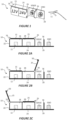
- a multi-voltage charging system 10 includes at least one housing 22 mounted on a support plate 20. Although illustrated as a single housing in the figures, it will be appreciated that the housing 22 may include multiple separate housings joined together and/or mounted separately.
- the housing 22 includes a first compartment 18 and a second compartment 28 in which a first charging terminal 12 and a second charging terminal 24 are positioned, respectively.
- the charging terminals 12, 24 may be provided as conductive metallic posts that are electrically connected to an electronics system of a vehicle.
- Each of the first and second compartments 18, 28 is covered by respective first and second access doors 15, 25 that cover the respective compartments and physically obstruct access to the charging terminal 12, 24 provided within the respective compartment.
- the first charging terminal 12 may be connected to a 12V electrical subsystem of a vehicle on which the multi-voltage charging system 10 is provided, and the second charging terminal 24 may be connected to a 24V electrical subsystem of the vehicle.
- the multi-voltage charging system 10 is illustrated as having two charging terminals, the system may have more charging terminals to support additional electrical subsystems having different voltage levels, such as 36V, 48V, etc.
- the open position Figure 2C
- the first charging terminal 12 is exposed for access by an operator.
- the closed position Figure 2A
- the first charging terminal 12 is obstructed from access by an operator.
- the first access door 15 may be connected to the housing 22 by a first spring-biased hinge 16 which is biased to move the first access door to the open position when the first access door 15 is unlatched, while the second access door 25 may be connected to the housing 22 by a second spring-biased hinge 26 which is biased to move the second access door to the open position when the second access door 25 is unlatched. That is, when one of the access doors is unlatched, it will spring open to provide physical access to the underlying charging terminal. To close the door, an operator may manually push the access door 15, 25 shut until it latches in place in the closed position.
- the multi-voltage charging system 10 may further include a first releasable latching mechanism 40 ( Figures 6A-6H ) that is configured to latch the first access door 15 in the closed position and a second releasable latching mechanism 40 that is configured to latch the second access door 25 in the closed position.
- a first releasable latching mechanism 40 ( Figures 6A-6H ) that is configured to latch the first access door 15 in the closed position
- a second releasable latching mechanism 40 that is configured to latch the second access door 25 in the closed position.
- the first and second releasable latching mechanisms 40 may cooperate with latching pins or features 50 provided on the first and second access doors 15, 25.
- the multi-voltage charging system 10 may further include a voltage sensing terminal SENSE and a ground terminal GND that may optionally be separated by a divider 36.
- a voltage sensing terminal SENSE and a ground terminal GND that may optionally be separated by a divider 36.
- an operator connects a ground connector from an external charging source to the ground terminal GND and connects a charging connector 11 from the external charging source to the voltage sensing terminal SENSE.
- the multi-voltage charging system 10 includes a door release circuit 60 ( Figures 3, 4 , and 5B ) coupled to the voltage sensing terminal SENSE and to the first and second releasable latching mechanisms 40.
- the door release circuit 60 is configured to sense a charging voltage applied to the voltage sensing terminal and selectively operate the first and second releasable latching mechanisms 40 to open the first access door 15 or the second access door 25 depending on the voltage applied at the sensing terminal SENSE.
- the door release circuit 60 may operate to cause the first releasable latching mechanism 40 to open the first access door 15, and if the charging voltage applied to the voltage sensing terminal SENSE is within a second acceptable voltage range, such as between 24 volts and 30 volts, the door release circuit 60 may operate to cause the second releasable latching mechanism 40 to open the second access door 25. If the charging voltage applied to the voltage sensing terminal SENSE is outside both the first acceptable voltage range and the second acceptable voltage range, the door release circuit 60 may operate to keep both the first access door 15 and the second access door 25 latched and closed.
- a first acceptable voltage range such as between 12 volts and 16 volts
- the door release circuit 60 may operate to cause the first releasable latching mechanism 40 to open the first access door 15
- a second acceptable voltage range such as between 24 volts and 30 volts
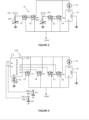
- a door release circuit 60 is illustrated in Figure 3 .
- the door release circuit comprises first through fourth transistor switches Q1 to Q4.
- the first through fourth transistor switches Q1 to Q4 are illustrated as MOSFET switches; however, it will be appreciated that other types of electrically controlled switches, such as bipolar junction transistor (BJT) switches, junction field effect transistor (JFET) switches, thyristors, or other types of elements may be used to form the transistor switches.
- BJT bipolar junction transistor
- JFET junction field effect transistor
- thyristors thyristors
- the first through fourth transistor switches Q1 to Q4 are illustrated as individual transistors, it will be appreciated that one or more of the first through fourth transistor switches Q1 to Q4 may include a plurality of transistors and/or other circuit elements connected together to form switching circuits when properly arranged.
- Control terminals, such as gate terminals, of the first through fourth transistor switches Q1 to Q4 are connected to the voltage sensing terminal SENSE, so that a voltage applied to the voltage sensing terminal SENSE will appear at the gate terminals of the first through fourth transistor switches Q1 to Q4.
- Input terminals, such as source terminals, of the second and fourth transistor switches Q2 and Q4 are connected to an output of a voltage regulator 92 that is arranged to supply a regulated DC voltage of, for example, five volts.
- a rectifier 94 may be provided at the output of the voltage regulator 92 between the voltage regulator 92 and the input terminals of the second and fourth transistor switches Q2 and Q4. The rectifier 94 may be arranged to obstruct a voltage from the second and fourth transistor switches Q2 and Q4 from being applied to the output of the voltage regulator 92.
- An output terminal, e.g. a drain terminal, of the second transistor switch Q2 is connected to an input (source) terminal of the first transistor switch Q1, and a drain terminal of the fourth transistor switch Q2 is connected to a source terminal of the third transistor switch Q3.
- An output (drain) terminal of the first transistor switch Q1 is coupled to a solenoid 80A which controls a first piston 78A, while a drain terminal of the third transistor switch Q3 is coupled to a solenoid 80B which controls a second piston 78B.
- the first piston 78A operates the releasable latch mechanism 40 to selectively unlatch the first access door 15, while the second piston 78B operates the releasable latch mechanism 40 to selectively unlatch the second access door 25.
- the first through fourth transistor switches Q1 to Q4 have respective different threshold voltages.
- the first transistor switch Q1 includes a normally ON depletion mode MOSFET that has a threshold voltage of 16V
- the second transistor switch Q2 includes a normally OFF enhancement mode MOSFET that has a threshold voltage of 12V.
- the third transistor switch Q3 includes a normally ON depletion mode MOSFET that has a threshold voltage of 30V
- the fourth transistor switch Q4 includes a normally OFF enhancement mode MOSFET that has a threshold voltage of 24V.
- the fourth transistor switch Q4 turns ON while the third transistor switch Q3 remains ON, thereby applying the voltage output by the voltage regulator 92 to the second solenoid 80B, which moves the second piston 78B to cause the releasable latching mechanism 40 to unlatch the second access door 25.
- the first transistor switch Q1 When the voltage applied to the voltage sensing terminal SENSE is greater than 16 volts and less than 24 volts, the first transistor switch Q1 is turned OFF, obstructing the voltage output by the voltage regulator 92 from being applied to the first solenoid 80A, and the fourth transistor switch Q4 remains OFF, obstructing the voltage output by the voltage regulator 92 from being applied to the second solenoid 80B.
- Table 1 The operation of the door release circuit 60 is summarized in Table 1.
- the 12V access door 15 is opened only when the applied voltage is between 12V and 15V, while the 24V access door 25 is opened only when the applied voltage is between 24V and 29V. In all other cases, both access doors remain closed.
- the multi-voltage charging system 10 could be modified to support additional voltage ranges by providing additional charging terminals in additional compartments. Moreover, it will be appreciated that the charging system 10 could be modified to support only a single voltage range by providing only a single charging terminal in a single compartment and modifying the door release circuit 60 to check for the single voltage range. Such a single terminal system may still physically restrict access to the single charging terminal unless an appropriate charging voltage is sensed at the voltage sensing terminal.
- FIG. 4 illustrates a door release circuit 60B according to further embodiments.
- the door release circuit 60B includes first to fourth transistor switches Q5, Q6, Q7 and Q8, each of which has a control terminal (gate) connected to the voltage sensing terminal SENSE.
- each of the first to fourth transistor switches Q5, Q6, Q7 and Q8 includes a normally OFF enhancement mode MOSFET.
- BJT switches, JFET switches, thyristors, or other types of elements may be used to form the transistor switches.
- first through fourth transistor switches Q5 to Q8 are illustrated as individual transistors, it will be appreciated that one or more of the first through fourth transistor switches Q5 to Q8 may include a plurality of transistors and/or other circuit elements connected together to form switching circuits when properly arranged.
- Each of the first to fourth transistor switches Q5, Q6, Q7 and Q8 has a different threshold voltage at which the transistor turns ON.
- transistor switch Q5 may have a turn on voltage of 12 volts
- transistor switch Q6 may have a turn on voltage of 16 volts
- transistor switch Q7 may have a turn on voltage of 24 volts
- transistor switch Q8 may have a turn on voltage of 30 volts.
- Input terminals, such as source terminals, of each of the first to fourth transistor switches Q5, Q6, Q7 and Q8 are connected to an output of a voltage regulator 92 that is arranged to supply a regulated DC voltage of, for example, five volts.
- a rectifier 94 may be provided at the output of the voltage regulator 92 between the voltage regulator 92 and the input terminals of the first to fourth transistor switches Q5 to Q8. The rectifier 94 may be arranged to obstruct a voltage from the first to fourth transistor switches Q5 to Q8 from being applied to the output of the voltage regulator 92.
- Output terminals, such as drain terminals, of each of the first to fourth transistor switches Q5 to Q8 are connected to respective data inputs D0 to D3 of a microcontroller 100.
- the microcontroller 100 includes three data outputs, namely, A0, A1 and INC.
- Output A0 is connected to the first solenoid 80A which operates the first piston 78A to unlatch the first access door 15 that covers the 12V charging terminal, while output A1 is connected to the second solenoid 80B which operates the second piston 78B to unlatch the second access door 25 that covers the 24V charging terminal.
- the INC output drives an indicator lamp, such as LED 96.
- circuit diagram of Figure 4 is a highly simplified diagram, and that other components may be included in a final design, such as driver circuits, bias circuits, current limiting resistors, etc.
- the microcontroller 100 may not be capable of directly supplying sufficient current from an output pin to operate a solenoid.
- a current limiting resistor would be provided in series with the LED 96 to prevent overcurrent. Such modifications are within the ordinary skill in the art and are omitted for clarity.
- the microcontroller 100 may, for example, be an 8- 16- or 32-bit microcontroller.
- the microcontroller 100 may include a 16F1507 8-bit programmable microcontroller manufactured by Microchip Technology Inc. or similar device.
- the microcontroller 100 sets the output signals A0, A1 and INC in response to the input signals D0 to D3. In particular, the microcontroller 100 sets the output signal A0 to HIGH so that the first solenoid 80A is activated to open the first access door 15 when the input voltage is greater than 12 volts but less than 16 volts (i.e., when input D0 is HIGH and inputs D1 to D3 are LOW).
- the microcontroller 100 sets the output signal A1 to HIGH so that the second solenoid 80B is activated to open the second access door 25 when the input voltage is greater than 24 volts but less than 30 volts (i.e., when inputs D0, D1 and D2 are HIGH and input D3 is LOW). In all other instances, the microcontroller 100 sets the output signal INC to HIGH to cause the indicator lamp 96 to light to indicate that an improper voltage (i.e. a voltage that was not between 12 and 16 volts or between 24 and 30 volts) was applied.
- an improper voltage i.e. a voltage that was not between 12 and 16 volts or between 24 and 30 volts
- door release circuit 60B of Figure 4 could be modified to support additional voltages by providing additional inputs and outputs to the microcontroller 110 and by providing additional solenoids to operate additional access doors.
- FIGS 5A and 5B illustrate a multi-voltage charging apparatus 110 according to further embodiments.
- the multi-voltage charging apparatus 110 includes a charging terminal CHARGE and a ground terminal GND mounted on a support plate 20.
- the charging terminal CHARGE and the ground terminal GND may optionally be separated by a divider 36.
- the multi-voltage charging apparatus 110 includes a coupling circuit 160 that selectively couples the charging terminal CHARGE to an internal charging node 112, 124 based on a voltage level applied to the charging terminal CHARGE.
- the coupling circuit 160 includes first to fourth transistor switches Q5, Q6, Q7 and Q8, each of which has a control terminal (gate) connected to the charging terminal CHARGE, and a microcontroller 100 including inputs D0 to D3 coupled to outputs of the respective transistor switches Q5, Q6, Q7 and Q8 and outputs A0 and A1.
- the configuration of the microcontroller 100, the transistor switches Q5, Q6, Q7 and Q8, the indicator lamp 96 and the voltage regulator 92 is similar to that shown in the door release circuit 60B of Figure 4 and further description thereof will be omitted for brevity except for differences in the circuits.
- the first output A0 is connected to a first solid state relay 102A, while the second output A1 is connected to a second solid state relay 102B.
- the first solid state relay 102A includes a photodiode and a photosensitive relay circuit that is configured to conduct when the photodiode is energized.
- the LED in the first solid state relay 102A is energized, which activates the photosensitive relay circuit therein. This causes the charging node CHARGE to be coupled to an internal 12 volt charging node 112, and allows a 12-volt battery system to which the internal 12 volt charging node 112 is connected to be charged by the external charge source.
- the LED in the second solid state relay 102B is energized, which activates the photosensitive relay circuit therein.
- This causes the charging node CHARGE to be coupled to an internal 24 volt charging node 124, and allows a 24-volt battery system to which the internal 24 volt charging node 124 is connected to be charged by the external charge source.
- a first indicator lamp 104A is coupled to the first output A0 to indicate when the 12V system is being charged, while a second indicator lamp 104B is coupled to the second output A1 to indicate when the 24V system is being charged.
- multi-voltage charging apparatus 110 of Figures 5A and 5B could be modified to support additional voltages by providing additional inputs and outputs to the microcontroller 110 and by providing additional solid state relays.
- the microcontroller 100 sets the output signals A0, A1 and INC in response to the input signals D0 to D3. In particular, the microcontroller 100 sets the output signal A0 to HIGH so that the first solid state relay 102A is activated to connect the charging terminal CHARGE to the 12 V internal charging node 112 when the input voltage is greater than 12 volts but less than 16 volts (i.e., when input D0 is HIGH and inputs D1 to D3 are LOW).
- the microcontroller 100 sets the output signal A1 to HIGH so that the second solid state relay 102B is activated to connect the charging terminal CHARGE to the 24 V internal charging node 124 when the input voltage is greater than 24 volts but less than 30 volts (i.e., when inputs D0, D1 and D2 are HIGH and input D3 is LOW).
- the microcontroller 100 sets the output signal INC to HIGH to cause the indicator lamp 96 to light to indicate that an improper voltage (i.e. a voltage that was not between 12 and 16 volts or between 24 and 30 volts) was applied.
- the operation of the coupling circuit 160 is the same as that shown in Table 2 for the door release circuit 60B.
- the microcontroller 100 may latch the output signal A0, A1 at HIGH so that the solid state relay 102A, 102B that was activated remains on even if the input voltage at the charging terminal CHARGE drops when the starter of the vehicle is engaged.
- separate resettable latch circuits may be provided between the microcontroller 100 and the solid state relays 102A, 102B.
- the design of resettable latch circuits, such as SR flip flop circuits, is well known in the art.
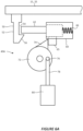
- Figures 6A and 6B illustrate a releasable latching mechanism 40A according to some embodiments.
- the releasable latching mechanism 40A includes a latching pin 50 including a body 52, a notch 54 in the body 52 and a wedge 56 at the end of the body 52.
- the latching pin 50 is affixed to one of the access doors 15, 25.
- a latching arm 62 extends from a housing 60 into the notch 54 when the access door 15, 25 is in the latched (closed) position.
- the latching arm 62 is biased against the latching pin 50 by a bias spring 66 within the housing 60.
- An extension 65 of the latching arm 62 extends from the housing 60 in a longitudinal slot (not shown) that allows the latching arm 60 and the extension 65 to move longitudinally within the housing 60.
- a rotating cam 72 includes a tooth 74 that engages the extension 65 of the latching arm 62 to move the latching arm 62 away from the latching pin 50 when the cam 72 is rotated in the clockwise direction.
- the bias spring 66 pushes the latching arm back towards the latching pin 50.
- the cam 72 is rotated by a solenoid 80 that drives a piston 78 attached to the cam 72 by a pin 76.
- the solenoid 80 is controlled by a circuit, such as the door release circuit 60, 60B shown in Figures 3 and 4 .
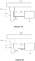
- Figures 6C and 6DB illustrate a simplified releasable latching mechanism 40B according to further embodiments.
- the releasable latching mechanism 40A includes a latching pin 50 including a body 52, a notch 54 in the body 52 and a wedge 56 at the end of the body 52.
- the latching pin 50 is affixed to one of the access doors 15, 25.
- a rotating cam 72 is connected to a latching arm 65 that holds the latching pin in place when held in the latched position shown in Figure 6C , and rotates away from the latching pin 50 to an unlatched position when the cam 72 is rotated in the clockwise direction.
- a coil spring 75 in the cam urges the cam to rotate back in the counterclockwise direction, pushing the latching arm back towards the latching pin 50.
- the cam 72 is rotated in the clockwise direction by a solenoid 80 that drives a piston 78 attached to the cam 72 by a pin 76.
- the solenoid 80 is controlled by a circuit, such as the door release circuit 60, 60B shown in Figures 3 and 4 .
- FIGS. 6E and 6F illustrate an even more simplified releasable latching mechanism 40C in which a latching arm 67 is driven directly as a piston by a solenoid 80 to engage or disengage a latching pin 50 to latch and unlatch an access door 15, 25.
- FIGS 6G and 6H illustrate a magnetic releasable latching mechanism 40D that includes a ferrous latching arm 68 mounted in a housing 69 and biased against the latching pin 50 by a spring 73.
- a coil 81 acts as an electromagnet to move the ferrous latching arm 68 out of engagement with the latching pin 50 to unlatch the access door 15, 25.
- the coil 81 is energized by a signal generated by a circuit, such as the door release circuit 60, 60B shown in Figures 3 and 4 .
- latching mechanisms may be used to selectively unlatch one or more access doors that provide access to charging terminals.
- Some embodiments of the inventive concepts described herein are not limited by the particular latching mechanism employed.
- the terms “comprise”, “comprising”, “comprises”, “include”, “including”, “includes”, “have”, “has”, “having”, or variants thereof are open-ended, and include one or more stated features, integers, elements, steps, components or functions but do not preclude the presence or addition of one or more other features, integers, elements, steps, components, functions or groups thereof.
- the common abbreviation “e.g.” which derives from the Latin phrase “exempli gratia,” may be used to introduce or specify a general example or examples of a previously mentioned item, and is not intended to be limiting of such item.
- the common abbreviation “i.e.”, which derives from the Latin phrase “id est,” may be used to specify a particular item from a more general recitation.
Landscapes
- Engineering & Computer Science (AREA)
- Power Engineering (AREA)
- Mechanical Engineering (AREA)
- Physics & Mathematics (AREA)
- Electromagnetism (AREA)
- Transportation (AREA)
- Manufacturing & Machinery (AREA)
- Chemical & Material Sciences (AREA)
- Chemical Kinetics & Catalysis (AREA)
- Electrochemistry (AREA)
- General Chemical & Material Sciences (AREA)
- Charge And Discharge Circuits For Batteries Or The Like (AREA)
Description
- The inventive concepts relate to vehicle electrical systems, and in particular to multi-voltage battery systems for vehicles.
- Some vehicles, including heavy construction vehicles, may include 24 volt (24V) electrical systems for powering various loads in the vehicle. A 24V vehicle electrical system typically includes first and second 12-volt (12V) batteries, namely, a lower battery and an upper battery, arranged in series to provide a total of 24 volts for powering 24V loads. In this arrangement, the batteries are referred to as the "lower battery" and the "upper battery," because the positive terminal of the upper battery is at a higher electric potential than the positive terminal of the lower battery. Thus, 24V loads can be powered from the positive terminal of the upper battery, while 12V loads can be powered from the positive terminal of the lower battery. When the engine of the vehicle is running, the batteries are charged by a 24V alternator that is connected across both batteries.
- In the event that one of the batteries has insufficient charge to operate the vehicle, it is important for there to be a safe and simple way for an operator to jump start the vehicle from either a 12V source or a 24V source. However, attaching a 24V source to a 12V electrical system can damage the 12V electrical system.
-
US 2014091761 A1 discloses a multi-voltage charging apparatus according to the preamble of claim 1. - One embodiment of the inventive concepts is directed to a multi-voltage charging apparatus that includes at least one housing including a first compartment and a second compartment, a first access door connected to the housing and covering the first compartment, the first access door being movable from an open position to a closed position, a second access door connected to the housing and covering the second compartment, the second access door being movable from an open position to a closed position, a first releasable latching mechanism configured to latch the first access door in the closed position, a second releasable latching mechanism configured to latch the second access door in the closed position, a first charging terminal in the first compartment, a second charging terminal in the second compartment, a voltage sensing terminal, and a door release circuit coupled to the voltage sensing terminal and to the first and second releasable latching mechanisms and configured to sense a charging voltage applied to the voltage sensing terminal. The door release circuit is configured to selectively unlatch the first releasable latching mechanism in response to a first voltage being applied to the voltage sensing terminal, and to selectively unlatch the second releasable latching mechanism in response to a second voltage being applied to the voltage sensing terminal, the second voltage being different from the first voltage.
- A charging apparatus according to further embodiments includes at least one housing including a compartment, an access door connected to the housing and covering the compartment, the access door being movable from an open position to a closed position, a releasable latching mechanism configured to latch the access door in the closed position, a charging terminal in the compartment, a voltage sensing terminal, and a door release circuit coupled to the voltage sensing terminal and to the releasable latching mechanisms and configured to sense a charging voltage applied to the voltage sensing terminal.
- A charging apparatus according to further embodiments includes a charging terminal, a ground terminal, and a coupling circuit coupled to the charging terminal, the coupling circuit is configured to sense a charging voltage applied to the charging terminal and to selectively couple the charging terminal to a first charging node in response to a first voltage being applied to the charging terminal, and to selectively couple the charging terminal to a second charging node in response to a second voltage being applied to the voltage sensing terminal, the second voltage being different from the first voltage.
- Other apparatus and/or methods for battery charging will be or become apparent to one with skill in the art upon review of the following drawings and shall be included within this description and protected by the accompanying claims. Moreover, it is intended that all embodiments disclosed herein can be implemented separately or combined in any way and/or combination unless expressly excluded.
- According to one aspect, a multi-voltage charging apparatus includes at least one housing including a first compartment and a second compartment, a first access door connected to the housing and covering the first compartment, the first access door being movable from an open position to a closed position, a second access door connected to the housing and covering the second compartment, the second access door being movable from an open position to a closed position, a first releasable latching mechanism configured to latch the first access door in the closed position, a second releasable latching mechanism configured to latch the second access door in the closed position, a first charging terminal in the first compartment, a second charging terminal in the second compartment, a voltage sensing terminal, and a door release circuit coupled to the voltage sensing terminal and to the first and second releasable latching mechanisms and configured to sense a charging voltage applied to the voltage sensing terminal. The door release circuit is configured to selectively unlatch the first releasable latching mechanism in response to a first voltage being applied to the voltage sensing terminal, and to selectively unlatch the second releasable latching mechanism in response to a second voltage being applied to the voltage sensing terminal, the second voltage being different from the first voltage.
- According to a further aspect, the first releasable latching mechanism includes a first solenoid and the second releasable latching mechanism includes a second solenoid.
- According to a further aspect, the door release circuit includes a voltage regulator configured to supply a third voltage, and a sensing node coupled to the voltage sensing terminal.
- According to a further aspect, the door release circuit includes a first transistor switch having an output terminal coupled to the first solenoid and a control terminal coupled to the sensing node, and a second transistor switch coupled in series with the first transistor switch having an input terminal coupled to the voltage regulator, an output terminal coupled to an input terminal of the first transistor switch, and a control terminal coupled to the sensing node.
- According to a further aspect, the first transistor switch includes a depletion mode MOSFET that is configured to turn off in response to a first voltage being applied to the sensing node, and the second transistor switch includes an enhancement mode MOSFET that is configured to turn on in response to a second voltage being applied to the sensing node, the first voltage is higher than the second voltage.
- According to a further aspect, the multi-voltage charging apparatus includes a third transistor switch having an output terminal coupled to the second solenoid and a control terminal coupled to the sensing node, a fourth transistor switch coupled in series with the third transistor switch having an input terminal coupled to the voltage regulator, an output terminal coupled to an input terminal of the third transistor switch, and a control terminal coupled to the sensing node.
- According to a further aspect, the third transistor switch includes a depletion mode MOSFET that is configured to turn off in response to a third voltage being applied to the sensing node, and the fourth transistor switch includes an enhancement mode MOSFET that is configured to turn on in response to a fourth voltage being applied to the sensing node, the third voltage is higher than the fourth voltage, and the second voltage is higher than the third voltage.
- According to a further aspect, the first transistor switch and the second transistor switch are arranged to apply the third voltage that is output by the voltage regulator to the first solenoid when a voltage supplied applied to the sensing node is greater than the second voltage and less than the first voltage.
- According to a further aspect, the third transistor switch and the fourth transistor switch are arranged to apply the third voltage that is output by the voltage regulator to the second solenoid when the voltage supplied applied to the sensing node is greater than the fourth voltage and less than the third voltage.
- According to a further aspect, the multi-voltage charging apparatus includes a rectifier diode between the voltage regulator and the input terminal of the second transistor switch.
- According to a further aspect, the door release circuit includes a microcontroller, and first, second, third and fourth transistor switches, each of the first, second, third and fourth transistor switches including a control terminal coupled to the sensing node, an output terminal coupled to the microcontroller, and an input terminal coupled to the voltage regulator. The first and second solenoids are coupled to the microcontroller, and the microcontroller is configured to control the first and second solenoids in response to signals output by the first, second, third and fourth transistors.
- According to a further aspect, the first, second, third and fourth transistor switches include normally off enhancement mode MOSFETs, the first, second, third and fourth transistor switches have respective first, second, third and fourth different turn-on voltages.
- According to a further aspect, the microcontroller is configured to activate the first solenoid when a voltage applied to the sensing node is between the third and fourth turn-on voltages, and the microcontroller is configured to activate the second solenoid when the voltage applied to the sensing node is between the first and second turn-on voltages.
- According to a further aspect, the multi-voltage charging apparatus includes a light emitting diode (LED) coupled to the microcontroller, the microcontroller is configured to cause the LED to emit light in response to the voltage applied at the sensing node not being between the first voltage and the second voltage or between the third voltage and the fourth voltage.
- According to a further aspect, the multi-voltage charging apparatus includes a rectifier diode coupled to an output of the voltage regulator.
- A charging apparatus according to an aspect includes at least one housing including a compartment, an access door connected to the housing and covering the compartment, the access door being movable from an open position to a closed position, a releasable latching mechanism configured to latch the access door in the closed position, a charging terminal in the compartment, a voltage sensing terminal, and a door release circuit coupled to the voltage sensing terminal and to the releasable latching mechanisms and configured to sense a charging voltage applied to the voltage sensing terminal.
- According to a further aspect, the door release circuit is configured to selectively unlatch the releasable latching mechanism in response to a voltage within a predetermined voltage range being applied to the voltage sensing terminal.
- A charging apparatus according to a still further aspect includes a charging terminal, a ground terminal, and a coupling circuit coupled to the charging terminal, the coupling circuit is configured to sense a charging voltage applied to the charging terminal and to selectively couple the charging terminal to a first charging node in response to a first voltage being applied to the charging terminal, and to selectively couple the charging terminal to a second charging node in response to a second voltage being applied to the voltage sensing terminal, the second voltage being different from the first voltage.
- According to a further aspect, the coupling circuit includes a voltage regulator configured to supply a third voltage, a microcontroller, first, second, third and fourth transistor switches, each of the first, second, third and fourth transistor switches including a control terminal coupled to the charging node, an output terminal coupled to the microcontroller, and an input terminal coupled to the voltage regulator, a first relay coupled to the microcontroller, the charging terminal, and the first charging node, and a second relay coupled to the microcontroller, the charging terminal, and the second charging node. The microcontroller is configured to cause the first relay to controllably couple the charging terminal to the first charging node and the second relay to controllably couple the charging terminal to the second charging node in response to signals output by the first, second, third and fourth transistor switches.
- According to a further aspect, the first, second, third and fourth transistor switches include normally off enhancement mode MOSFETs, the first, second, third and fourth transistor switches have respective first, second, third and fourth different turn-on voltages.
- According to a further aspect, the relays include optically triggered relays that isolate the charging terminal and the first and second charging nodes from the microcontroller.
- The accompanying drawings, which are included to provide a further understanding of the disclosure and are incorporated in and constitute a part of this application, illustrate certain non-limiting embodiments of inventive concepts. In the drawings:
-
Figure 1 is a perspective view of a multi-voltage charging apparatus according to some embodiments. -
Figures 2A, 2B and 2C are side views a multi-voltage charging apparatus according to some embodiments. -
Figure 3 is a simplified circuit diagram of a door release circuit according to some embodiments. -
Figure 4 is a simplified circuit diagram of a door release circuit according to some embodiments. -
Figure 5A is a side view of a multi-voltage charging apparatus according to some embodiments. -
Figure 5B is a simplified circuit diagram of a coupling circuit according to some embodiments. -
Figures 6A and6B illustrate a releasable latching mechanism according to some embodiments. -
Figures 6C and 6D illustrate a releasable latching mechanism according to further embodiments. -
Figures 6E and 6F illustrate a releasable latching mechanism according to further embodiments. -
Figures 6G and 6H illustrate a releasable latching mechanism according to further embodiments. - As noted in the Background section above, multi-voltage vehicles may have both a 12V electrical system and a 24V electrical system. In the event a vehicle operator needs to jump start the system, it is desirable to be able to provide external charge from a 12V source or a 24V source. However, attaching a 24V source to a 12V electrical system can damage the 12V electrical system of the vehicle. Attaching an external charge source to a vehicle for jump starting is often performed in harsh environments, possibly in the dark or with little available light. It is possible that an operator may incorrectly attach a charging source to the wrong charging terminal on the vehicle being jump started, e.g., attaching a 24V charging source to a 12V terminal. Some vehicles may even have more than two electrical systems, e.g., 12V, 24V and 48V systems in the same vehicle.
- Some embodiments address one or more of the issues described above by providing a multi-voltage charging apparatus that physically controls access to first and second charging terminals, such as a 12V charging terminal and a 24V charging terminal, so that only the correct charging terminal is available for connection to an external charge source. These embodiments sense the external charging voltage at an exposed sensing terminal and then selectively provide physical access only to the charging terminal corresponding to the external charging voltage.
- Some further embodiments address one or more of the issues described above by sensing an external charging voltage and selectively connecting the charging voltage only to an internal charging node that corresponds to the external charging voltage.
- Various embodiments are described herein by way of non-limiting examples in the context of a multi-voltage vehicle electrical system. It is to be understood that the embodiments are not limited to the particular configurations disclosed herein. Moreover, although various embodiments are described in the context of dual-voltage vehicle electrical systems, it will be appreciated that the concepts and embodiments described herein may be extended to vehicle electrical systems with more or less than two voltage subsystems. For example, in some embodiments, a multi-voltage charging system includes multiple charging terminals configured to accept different ranges of charging voltages. In other embodiments, only a single charging terminal configured to accept a single range of charging voltages is provided. In still other embodiments, a single charging terminal configured to accept a plurality of ranges of charging voltages is provided.
- Reference is now made to
Figure 1 , which is a perspective illustration of amulti-voltage charging system 10 according to some embodiments, and toFigures 2A to 2C , which are side views of themulti-voltage charging system 10. As shown therein, amulti-voltage charging system 10 according to some embodiments includes at least onehousing 22 mounted on asupport plate 20. Although illustrated as a single housing in the figures, it will be appreciated that thehousing 22 may include multiple separate housings joined together and/or mounted separately. Thehousing 22 includes afirst compartment 18 and asecond compartment 28 in which a first chargingterminal 12 and asecond charging terminal 24 are positioned, respectively. The chargingterminals second compartments second access doors terminal - The
first charging terminal 12 may be connected to a 12V electrical subsystem of a vehicle on which themulti-voltage charging system 10 is provided, and thesecond charging terminal 24 may be connected to a 24V electrical subsystem of the vehicle. However, other voltages may be used. Moreover, although themulti-voltage charging system 10 is illustrated as having two charging terminals, the system may have more charging terminals to support additional electrical subsystems having different voltage levels, such as 36V, 48V, etc. - The
first access door 15, which is connected to thehousing 22 covers thefirst compartment 18, is movable from an open position illustrated inFigure 2C to a closed position illustrated inFigure 2A . In the open position (Figure 2C ), the first chargingterminal 12 is exposed for access by an operator. In the closed position (Figure 2A ), the first chargingterminal 12 is obstructed from access by an operator. - The
second access door 25, which is connected to thehousing 22 covers thesecond compartment 28, is movable from an open position illustrated inFigure 2B to a closed position illustrated inFigure 2A . In the open position (Figure 2B ), thesecond charging terminal 24 is exposed for access by an operator. In the closed position (Figure 2A ), thesecond charging terminal 12 is obstructed from access by an operator. - The
first access door 15 may be connected to thehousing 22 by a first spring-biasedhinge 16 which is biased to move the first access door to the open position when thefirst access door 15 is unlatched, while thesecond access door 25 may be connected to thehousing 22 by a second spring-biasedhinge 26 which is biased to move the second access door to the open position when thesecond access door 25 is unlatched. That is, when one of the access doors is unlatched, it will spring open to provide physical access to the underlying charging terminal. To close the door, an operator may manually push theaccess door - The
multi-voltage charging system 10 may further include a first releasable latching mechanism 40 (Figures 6A-6H ) that is configured to latch thefirst access door 15 in the closed position and a second releasable latching mechanism 40 that is configured to latch thesecond access door 25 in the closed position. As will be described in more detail below, the first and second releasable latching mechanisms 40 may cooperate with latching pins or features 50 provided on the first andsecond access doors - Still referring to
Figures 1 and 2A-2C , themulti-voltage charging system 10 may further include a voltage sensing terminal SENSE and a ground terminal GND that may optionally be separated by adivider 36. To operate themulti-voltage charging system 10, an operator connects a ground connector from an external charging source to the ground terminal GND and connects a chargingconnector 11 from the external charging source to the voltage sensing terminal SENSE. Themulti-voltage charging system 10 includes a door release circuit 60 (Figures 3, 4 , and5B ) coupled to the voltage sensing terminal SENSE and to the first and second releasable latching mechanisms 40. Thedoor release circuit 60 is configured to sense a charging voltage applied to the voltage sensing terminal and selectively operate the first and second releasable latching mechanisms 40 to open thefirst access door 15 or thesecond access door 25 depending on the voltage applied at the sensing terminal SENSE. For example, in some embodiments, if the charging voltage applied to the voltage sensing terminal SENSE is within a first acceptable voltage range, such as between 12 volts and 16 volts, thedoor release circuit 60 may operate to cause the first releasable latching mechanism 40 to open thefirst access door 15, and if the charging voltage applied to the voltage sensing terminal SENSE is within a second acceptable voltage range, such as between 24 volts and 30 volts, thedoor release circuit 60 may operate to cause the second releasable latching mechanism 40 to open thesecond access door 25. If the charging voltage applied to the voltage sensing terminal SENSE is outside both the first acceptable voltage range and the second acceptable voltage range, thedoor release circuit 60 may operate to keep both thefirst access door 15 and thesecond access door 25 latched and closed. - Once one of the
access doors - A
door release circuit 60 according to some embodiments is illustrated inFigure 3 . As shown therein, the door release circuit comprises first through fourth transistor switches Q1 to Q4. The first through fourth transistor switches Q1 to Q4 are illustrated as MOSFET switches; however, it will be appreciated that other types of electrically controlled switches, such as bipolar junction transistor (BJT) switches, junction field effect transistor (JFET) switches, thyristors, or other types of elements may be used to form the transistor switches. Moreover, although the first through fourth transistor switches Q1 to Q4 are illustrated as individual transistors, it will be appreciated that one or more of the first through fourth transistor switches Q1 to Q4 may include a plurality of transistors and/or other circuit elements connected together to form switching circuits when properly arranged. - Control terminals, such as gate terminals, of the first through fourth transistor switches Q1 to Q4 are connected to the voltage sensing terminal SENSE, so that a voltage applied to the voltage sensing terminal SENSE will appear at the gate terminals of the first through fourth transistor switches Q1 to Q4. Input terminals, such as source terminals, of the second and fourth transistor switches Q2 and Q4 are connected to an output of a
voltage regulator 92 that is arranged to supply a regulated DC voltage of, for example, five volts. Arectifier 94 may be provided at the output of thevoltage regulator 92 between thevoltage regulator 92 and the input terminals of the second and fourth transistor switches Q2 and Q4. Therectifier 94 may be arranged to obstruct a voltage from the second and fourth transistor switches Q2 and Q4 from being applied to the output of thevoltage regulator 92. - An output terminal, e.g. a drain terminal, of the second transistor switch Q2 is connected to an input (source) terminal of the first transistor switch Q1, and a drain terminal of the fourth transistor switch Q2 is connected to a source terminal of the third transistor switch Q3. An output (drain) terminal of the first transistor switch Q1 is coupled to a
solenoid 80A which controls afirst piston 78A, while a drain terminal of the third transistor switch Q3 is coupled to asolenoid 80B which controls asecond piston 78B. Thefirst piston 78A operates the releasable latch mechanism 40 to selectively unlatch thefirst access door 15, while thesecond piston 78B operates the releasable latch mechanism 40 to selectively unlatch thesecond access door 25. - The first through fourth transistor switches Q1 to Q4 have respective different threshold voltages. In particular, the first transistor switch Q1 includes a normally ON depletion mode MOSFET that has a threshold voltage of 16V, while the second transistor switch Q2 includes a normally OFF enhancement mode MOSFET that has a threshold voltage of 12V. Likewise, the third transistor switch Q3 includes a normally ON depletion mode MOSFET that has a threshold voltage of 30V, while the fourth transistor switch Q4 includes a normally OFF enhancement mode MOSFET that has a threshold voltage of 24V. When a charging voltage applied to the voltage sensing terminal SENSE has a voltage level between 12 volts and 16 volts, the second transistor switch Q2 turns ON while the first transistor switch Q1 remains ON, thereby applying the voltage output by the
voltage regulator 92 to thefirst solenoid 80A, which moves thefirst piston 78A to cause the releasable latching mechanism 40 to unlatch thefirst access door 15. Similarly, when a charging voltage applied to the voltage sensing terminal SENSE has a voltage level between 24 volts and 30 volts, the fourth transistor switch Q4 turns ON while the third transistor switch Q3 remains ON, thereby applying the voltage output by thevoltage regulator 92 to thesecond solenoid 80B, which moves thesecond piston 78B to cause the releasable latching mechanism 40 to unlatch thesecond access door 25. - Note that when the voltage applied to the voltage sensing terminal SENSE is less than 12 volts, the second transistor switch Q2 and the fourth transistor switch Q4 remain OFF, obstructing the voltage output by the voltage regulator from being applied to either the first or
second solenoid second solenoid voltage regulator 92 from being applied to thefirst solenoid 80A, and the fourth transistor switch Q4 remains OFF, obstructing the voltage output by thevoltage regulator 92 from being applied to thesecond solenoid 80B. The operation of thedoor release circuit 60 is summarized in Table 1.Table 1 - Door Release Circuit Operation Applied Voltage Q1 state Q2 state Q3 state Q4 state 12V access door state 24V access door state 0V to 11V ON OFF ON OFF Closed Closed 12V to 15V ON ON ON OFF Open Closed 16V to 23V OFF ON ON OFF Closed Closed 24V to 29V OFF ON ON ON Closed Open 30V + OFF ON OFF ON Closed Closed - As can be seen in Table 1, the
12V access door 15 is opened only when the applied voltage is between 12V and 15V, while the24V access door 25 is opened only when the applied voltage is between 24V and 29V. In all other cases, both access doors remain closed. - It will be appreciated that the
door release circuit 60 ofFigure 3 could be modified to support additional voltages by providing additional pairs of transistor switches having threshold voltages that define additional acceptable voltage ranges and by providing additional solenoids to operate additional access doors. - It will further be appreciated that the
multi-voltage charging system 10 could be modified to support additional voltage ranges by providing additional charging terminals in additional compartments. Moreover, it will be appreciated that the chargingsystem 10 could be modified to support only a single voltage range by providing only a single charging terminal in a single compartment and modifying thedoor release circuit 60 to check for the single voltage range. Such a single terminal system may still physically restrict access to the single charging terminal unless an appropriate charging voltage is sensed at the voltage sensing terminal. -
Figure 4 illustrates a door release circuit 60B according to further embodiments. The door release circuit 60B includes first to fourth transistor switches Q5, Q6, Q7 and Q8, each of which has a control terminal (gate) connected to the voltage sensing terminal SENSE. In the embodiment illustrated inFigure 4 , each of the first to fourth transistor switches Q5, Q6, Q7 and Q8 includes a normally OFF enhancement mode MOSFET. However, it will be appreciated that other types of electrically controlled switches, such as BJT switches, JFET switches, thyristors, or other types of elements may be used to form the transistor switches. Moreover, although the first through fourth transistor switches Q5 to Q8 are illustrated as individual transistors, it will be appreciated that one or more of the first through fourth transistor switches Q5 to Q8 may include a plurality of transistors and/or other circuit elements connected together to form switching circuits when properly arranged. Each of the first to fourth transistor switches Q5, Q6, Q7 and Q8 has a different threshold voltage at which the transistor turns ON. For example, transistor switch Q5 may have a turn on voltage of 12 volts, transistor switch Q6 may have a turn on voltage of 16 volts, transistor switch Q7 may have a turn on voltage of 24 volts, and transistor switch Q8 may have a turn on voltage of 30 volts. - Input terminals, such as source terminals, of each of the first to fourth transistor switches Q5, Q6, Q7 and Q8 are connected to an output of a
voltage regulator 92 that is arranged to supply a regulated DC voltage of, for example, five volts. Arectifier 94 may be provided at the output of thevoltage regulator 92 between thevoltage regulator 92 and the input terminals of the first to fourth transistor switches Q5 to Q8. Therectifier 94 may be arranged to obstruct a voltage from the first to fourth transistor switches Q5 to Q8 from being applied to the output of thevoltage regulator 92. - Output terminals, such as drain terminals, of each of the first to fourth transistor switches Q5 to Q8 are connected to respective data inputs D0 to D3 of a
microcontroller 100. Themicrocontroller 100 includes three data outputs, namely, A0, A1 and INC. Output A0 is connected to thefirst solenoid 80A which operates thefirst piston 78A to unlatch thefirst access door 15 that covers the 12V charging terminal, while output A1 is connected to thesecond solenoid 80B which operates thesecond piston 78B to unlatch thesecond access door 25 that covers the 24V charging terminal. The INC output drives an indicator lamp, such asLED 96. - It will be appreciated that the circuit diagram of
Figure 4 is a highly simplified diagram, and that other components may be included in a final design, such as driver circuits, bias circuits, current limiting resistors, etc. For example, themicrocontroller 100 may not be capable of directly supplying sufficient current from an output pin to operate a solenoid. Likewise, in a practical implementation, a current limiting resistor would be provided in series with theLED 96 to prevent overcurrent. Such modifications are within the ordinary skill in the art and are omitted for clarity. - The
microcontroller 100 may, for example, be an 8- 16- or 32-bit microcontroller. For example, themicrocontroller 100 may include a 16F1507 8-bit programmable microcontroller manufactured by Microchip Technology Inc. or similar device. - When the voltage applied at the voltage sensing terminal is less than 12 volts, all four of the first to fourth transistor switches Q5 to Q8 are OFF. When the voltage applied at the voltage sensing terminal is greater than 12 volts but less than 16 volts, then the first transistor switch Q5 is ON, while the remaining three transistor switches Q6 to Q8 are OFF. When the voltage applied at the voltage sensing terminal is greater than 16 volts but less than 24 volts, then the first and second transistor switches Q5 and Q6 are ON, while the remaining two transistor switches Q7 and Q8 are OFF. When the voltage applied at the voltage sensing terminal is greater than 24 volts but less than 30 volts, then the first, second and third transistor switches Q5, Q6 and Q7 are ON, while the remaining transistor switch Q8 is OFF. Finally, when the voltage applied at the voltage sensing terminal is greater than 30 volts, all four transistor switches Q5 to Q8 are ON. The
microcontroller 100 sets the output signals A0, A1 and INC in response to the input signals D0 to D3. In particular, themicrocontroller 100 sets the output signal A0 to HIGH so that thefirst solenoid 80A is activated to open thefirst access door 15 when the input voltage is greater than 12 volts but less than 16 volts (i.e., when input D0 is HIGH and inputs D1 to D3 are LOW). Likewise, themicrocontroller 100 sets the output signal A1 to HIGH so that thesecond solenoid 80B is activated to open thesecond access door 25 when the input voltage is greater than 24 volts but less than 30 volts (i.e., when inputs D0, D1 and D2 are HIGH and input D3 is LOW). In all other instances, themicrocontroller 100 sets the output signal INC to HIGH to cause theindicator lamp 96 to light to indicate that an improper voltage (i.e. a voltage that was not between 12 and 16 volts or between 24 and 30 volts) was applied. - The operation of the door release circuit 60B is summarized in Table 2.
Table 2 - Door Release Circuit Operation Applied Voltage Input D0 Input D1 Input D2 Input D3 Output A0 Output A1 Output INC 0V to 11V LOW LOW LOW LOW LOW LOW HIGH 12V to 15V HIGH LOW LOW LOW HIGH LOW LOW 16V to 23V HIGH HIGH LOW LOW LOW LOW HIGH 24V to 29V HIGH HIGH HIGH LOW LOW HIGH LOW 30V + HIGH HIGH HIGH HIGH LOW LOW HIGH - It will be appreciated that the door release circuit 60B of
Figure 4 could be modified to support additional voltages by providing additional inputs and outputs to themicrocontroller 110 and by providing additional solenoids to operate additional access doors. -
Figures 5A and 5B illustrate amulti-voltage charging apparatus 110 according to further embodiments. Themulti-voltage charging apparatus 110 includes a charging terminal CHARGE and a ground terminal GND mounted on asupport plate 20. The charging terminal CHARGE and the ground terminal GND may optionally be separated by adivider 36. Themulti-voltage charging apparatus 110 includes acoupling circuit 160 that selectively couples the charging terminal CHARGE to aninternal charging node - Referring to
Figure 5B , thecoupling circuit 160 includes first to fourth transistor switches Q5, Q6, Q7 and Q8, each of which has a control terminal (gate) connected to the charging terminal CHARGE, and amicrocontroller 100 including inputs D0 to D3 coupled to outputs of the respective transistor switches Q5, Q6, Q7 and Q8 and outputs A0 and A1. The configuration of themicrocontroller 100, the transistor switches Q5, Q6, Q7 and Q8, theindicator lamp 96 and thevoltage regulator 92 is similar to that shown in the door release circuit 60B ofFigure 4 and further description thereof will be omitted for brevity except for differences in the circuits. - In the
coupling circuit 160, the first output A0 is connected to a firstsolid state relay 102A, while the second output A1 is connected to a secondsolid state relay 102B. The firstsolid state relay 102A includes a photodiode and a photosensitive relay circuit that is configured to conduct when the photodiode is energized. Thus, for example, when the first output A0 is HIGH, the LED in the firstsolid state relay 102A is energized, which activates the photosensitive relay circuit therein. This causes the charging node CHARGE to be coupled to an internal 12volt charging node 112, and allows a 12-volt battery system to which the internal 12volt charging node 112 is connected to be charged by the external charge source. Similarly, when the second output A1 is HIGH, the LED in the secondsolid state relay 102B is energized, which activates the photosensitive relay circuit therein. This causes the charging node CHARGE to be coupled to an internal 24volt charging node 124, and allows a 24-volt battery system to which the internal 24volt charging node 124 is connected to be charged by the external charge source. - A
first indicator lamp 104A is coupled to the first output A0 to indicate when the 12V system is being charged, while asecond indicator lamp 104B is coupled to the second output A1 to indicate when the 24V system is being charged. - It will be appreciated that the
multi-voltage charging apparatus 110 ofFigures 5A and 5B could be modified to support additional voltages by providing additional inputs and outputs to themicrocontroller 110 and by providing additional solid state relays. - When the voltage applied at the voltage sensing terminal is less than 12 volts, all four of the first to fourth transistor switches Q5 to Q8 are OFF. When the voltage applied at the voltage sensing terminal is greater than 12 volts but less than 16 volts, then the first transistor switch Q5 is ON, while the remaining three transistor switches Q6 to Q8 are OFF. When the voltage applied at the voltage sensing terminal is greater than 16 volts but less than 24 volts, then the first and second transistor switches Q5 and Q6 are ON, while the remaining two transistor switches Q7 and Q8 are OFF. When the voltage applied at the voltage sensing terminal is greater than 24 volts but less than 30 volts, then the first, second and third transistor switches Q5, Q6 and Q7 are ON, while the remaining transistor switch Q8 is OFF. Finally, when the voltage applied at the voltage sensing terminal is greater than 30 volts, all four transistor switches Q5 to Q8 are ON.
- The
microcontroller 100 sets the output signals A0, A1 and INC in response to the input signals D0 to D3. In particular, themicrocontroller 100 sets the output signal A0 to HIGH so that the firstsolid state relay 102A is activated to connect the charging terminal CHARGE to the 12 Vinternal charging node 112 when the input voltage is greater than 12 volts but less than 16 volts (i.e., when input D0 is HIGH and inputs D1 to D3 are LOW). Likewise, themicrocontroller 100 sets the output signal A1 to HIGH so that the secondsolid state relay 102B is activated to connect the charging terminal CHARGE to the 24 Vinternal charging node 124 when the input voltage is greater than 24 volts but less than 30 volts (i.e., when inputs D0, D1 and D2 are HIGH and input D3 is LOW). In all other instances, themicrocontroller 100 sets the output signal INC to HIGH to cause theindicator lamp 96 to light to indicate that an improper voltage (i.e. a voltage that was not between 12 and 16 volts or between 24 and 30 volts) was applied. The operation of thecoupling circuit 160 is the same as that shown in Table 2 for the door release circuit 60B. Once themicrocontroller 100 sets the output signal A0, A1 to HIGH, themicrocontroller 100 may latch the output signal A0, A1 at HIGH so that thesolid state relay microcontroller 100 and the solid state relays 102A, 102B. The design of resettable latch circuits, such as SR flip flop circuits, is well known in the art. -
Figures 6A and6B illustrate areleasable latching mechanism 40A according to some embodiments. Referring toFigures 6A and6B , thereleasable latching mechanism 40A includes a latchingpin 50 including abody 52, anotch 54 in thebody 52 and awedge 56 at the end of thebody 52. The latchingpin 50 is affixed to one of theaccess doors arm 62 extends from ahousing 60 into thenotch 54 when theaccess door arm 62 is biased against the latchingpin 50 by abias spring 66 within thehousing 60. Anextension 65 of the latchingarm 62 extends from thehousing 60 in a longitudinal slot (not shown) that allows the latchingarm 60 and theextension 65 to move longitudinally within thehousing 60. A rotatingcam 72 includes atooth 74 that engages theextension 65 of the latchingarm 62 to move the latchingarm 62 away from the latchingpin 50 when thecam 72 is rotated in the clockwise direction. When thecam 72 is rotated in the counterclockwise direction, thebias spring 66 pushes the latching arm back towards the latchingpin 50. - The
cam 72 is rotated by asolenoid 80 that drives apiston 78 attached to thecam 72 by apin 76. As described above, thesolenoid 80 is controlled by a circuit, such as thedoor release circuit 60, 60B shown inFigures 3 and 4 . -
Figures 6C and 6DB illustrate a simplifiedreleasable latching mechanism 40B according to further embodiments. Referring toFigures 6C and 6D , thereleasable latching mechanism 40A includes a latchingpin 50 including abody 52, anotch 54 in thebody 52 and awedge 56 at the end of thebody 52. The latchingpin 50 is affixed to one of theaccess doors cam 72 is connected to a latchingarm 65 that holds the latching pin in place when held in the latched position shown inFigure 6C , and rotates away from the latchingpin 50 to an unlatched position when thecam 72 is rotated in the clockwise direction. Acoil spring 75 in the cam urges the cam to rotate back in the counterclockwise direction, pushing the latching arm back towards the latchingpin 50. - The
cam 72 is rotated in the clockwise direction by asolenoid 80 that drives apiston 78 attached to thecam 72 by apin 76. As described above, thesolenoid 80 is controlled by a circuit, such as thedoor release circuit 60, 60B shown inFigures 3 and 4 . -
Figures 6E and 6F illustrate an even more simplifiedreleasable latching mechanism 40C in which alatching arm 67 is driven directly as a piston by asolenoid 80 to engage or disengage a latchingpin 50 to latch and unlatch anaccess door -
Figures 6G and 6H illustrate a magnetic releasable latching mechanism 40D that includes aferrous latching arm 68 mounted in ahousing 69 and biased against the latchingpin 50 by aspring 73. Acoil 81 acts as an electromagnet to move theferrous latching arm 68 out of engagement with the latchingpin 50 to unlatch theaccess door coil 81 is energized by a signal generated by a circuit, such as thedoor release circuit 60, 60B shown inFigures 3 and 4 . - From the foregoing description of various releasable latching mechanisms, it will be apparent that many different type of latching mechanisms may be used to selectively unlatch one or more access doors that provide access to charging terminals. Some embodiments of the inventive concepts described herein are not limited by the particular latching mechanism employed.
- When an element is referred to as being "connected", "coupled", "responsive", "mounted", or variants thereof to another element, it can be directly connected, coupled, responsive, or mounted to the other element or intervening elements may be present. In contrast, when an element is referred to as being "directly connected", "directly coupled", "directly responsive", "directly mounted" or variants thereof to another element, there are no intervening elements present. Like numbers refer to like elements throughout. As used herein, the singular forms "a", "an" and "the" are intended to include the plural forms as well, unless the context clearly indicates otherwise. Well-known functions or constructions may not be described in detail for brevity and/or clarity. The term "and/or" and its abbreviation "/" include any and all combinations of one or more of the associated listed items.
- It will be understood that although the terms first, second, third, etc. may be used herein to describe various elements/operations, these elements/operations should not be limited by these terms. These terms are only used to distinguish one element/operation from another element/operation. Thus, a first element/operation in some embodiments could be termed a second element/operation in other embodiments without departing from the teachings of present inventive concepts. The same reference numerals or the same reference designators denote the same or similar elements throughout the specification.
- As used herein, the terms "comprise", "comprising", "comprises", "include", "including", "includes", "have", "has", "having", or variants thereof are open-ended, and include one or more stated features, integers, elements, steps, components or functions but do not preclude the presence or addition of one or more other features, integers, elements, steps, components, functions or groups thereof. Furthermore, as used herein, the common abbreviation "e.g.", which derives from the Latin phrase "exempli gratia," may be used to introduce or specify a general example or examples of a previously mentioned item, and is not intended to be limiting of such item. The common abbreviation "i.e.", which derives from the Latin phrase "id est," may be used to specify a particular item from a more general recitation.
- Persons skilled in the art will recognize that certain elements of the above-described embodiments may variously be combined or eliminated to create further embodiments, and such further embodiments fall within the scope and teachings of inventive concepts. It will also be apparent to those of ordinary skill in the art that the above-described embodiments may be combined in whole or in part to create additional embodiments within the scope and teachings of inventive concepts. Thus, although specific embodiments of, and examples for, inventive concepts are described herein for illustrative purposes, various equivalent modifications are possible within the scope of inventive concepts, as those skilled in the relevant art will recognize. Accordingly, the scope of inventive concepts is determined from the appended claims and equivalents thereof.
Claims (13)
- A multi-voltage charging apparatus (10), comprising:a first compartment (18) and a second compartment (28) defined within at least one housing (22);a first charging terminal (12) in the first compartment (18);a second charging terminal (24) in the second compartment (28);a first access door (15) connected to the at least one housing (22) and covering the first compartment (18), the first access door (15) being movable from an open position to a closed position;a first releasable latching mechanism (40) configured to latch the first access door (15) in the closed position;characterised by further comprisinga second access door (25) connected to the at least one housing (22) and covering the second compartment (28), the second access door (25) being movable from an open position to a closed position;a second releasable latching mechanism (40) configured to latch the second access door (25) in the closed position;a voltage sensing terminal (SENSE); anda door release circuit (60) coupled to the voltage sensing terminal (SENSE) and to the first and second releasable latching mechanisms (40) and configured to sense a charging voltage applied to the voltage sensing terminal (SENSE);wherein the door release circuit (60) is configured to selectively unlatch the first releasable latching mechanism (40) in response to a first voltage being applied to the voltage sensing terminal (SENSE), and to selectively unlatch the second releasable latching mechanism (40) in response to a second voltage being applied to the voltage sensing terminal (SENSE), the second voltage being different from the first voltage.
- The multi-voltage charging apparatus (10) of Claim 1, wherein the first releasable latching mechanism (40) comprises a first solenoid (80A) and the second releasable latching mechanism (40) comprises a second solenoid (80B).
- The multi-voltage charging apparatus (10) of Claim 2, wherein the door release circuit (60) comprises:a voltage regulator (92) configured to supply a third voltage; anda sensing node coupled to the voltage sensing terminal (SENSE).
- The multi-voltage charging apparatus (10) of Claim 3, wherein the door release circuit (60) further comprises:a first transistor switch (Q1) having an output terminal coupled to the first solenoid (80A) and a control terminal coupled to the sensing node; anda second transistor switch (Q2) coupled in series with the first transistor switch (Q1) having an input terminal coupled to the voltage regulator (92), an output terminal coupled to an input terminal of the first transistor switch (Q1), and a control terminal coupled to the sensing node.
- The multi-voltage charging apparatus (10) of Claim 4, wherein the first transistor switch (Q1) comprises a depletion mode MOSFET that is configured to turn off in response to a first voltage being applied to the sensing node, and wherein the second transistor switch (Q2) comprises an enhancement mode MOSFET that is configured to turn on in response to a second voltage being applied to the sensing node, wherein the first voltage is higher than the second voltage.
- The multi-voltage charging apparatus (10) of Claim 5, further comprising:a third transistor switch (Q3) having an output terminal coupled to the second solenoid (80B) and a control terminal coupled to the sensing node;a fourth transistor switch (Q4) coupled in series with the third transistor switch (Q3) having an input terminal coupled to the voltage regulator (92), an output terminal coupled to an input terminal of the third transistor switch (Q3), and a control terminal coupled to the sensing node.
- The multi-voltage charging apparatus (10) of Claim 6, wherein the third transistor switch (Q3) comprises a depletion mode MOSFET that is configured to turn off in response to a third voltage being applied to the sensing node, and wherein the fourth transistor switch (Q4) comprises an enhancement mode MOSFET that is configured to turn on in response to a fourth voltage being applied to the sensing node, wherein the third voltage is higher than the fourth voltage, and wherein the second voltage is higher than the third voltage.
- The multi-voltage charging apparatus (10) of Claim 7, wherein the first transistor switch (Q1) and the second transistor switch (Q2) are arranged to apply the third voltage that is output by the voltage regulator (92) to the first solenoid (80A) when a voltage supplied applied to the sensing node is greater than the second voltage and less than the first voltage.
- The multi-voltage charging apparatus (10) of Claim 8, wherein the third transistor switch (Q3) and the fourth transistor switch (Q4) are arranged to apply the third voltage that is output by the voltage regulator (92) to the second solenoid (80B) when the voltage supplied applied to the sensing node is greater than the fourth voltage and less than the third voltage.
- The multi-voltage charging apparatus (10) of any of Claims 4-9, further comprising a rectifier diode (94) between the voltage regulator (92) and the input terminal of the second transistor switch (Q2).
- The multi-voltage charging apparatus (10) of Claim 3, wherein the door release circuit (60) further comprises:a microcontroller (100); andfirst, second, third and fourth transistor switches (Q5, Q6, Q7, Q8), each of the first, second, third and fourth transistor switches comprising a control terminal coupled to the sensing node, an output terminal coupled to the microcontroller (100), and an input terminal coupled to the voltage regulator (92);wherein the first and second solenoids (80A, 80B) are coupled to the microcontroller (100), and wherein the microcontroller (100) is configured to control the first and second solenoids (80A, 80B) in response to signals output by the first, second, third and fourth transistors (Q5, Q6, Q7, Q8).
- The multi-voltage charging apparatus (10) of Claim 11,
wherein the first, second, third and fourth transistor switches (Q5, Q6, Q7, Q8) comprise normally off enhancement mode MOSFETs, wherein the first, second, third and fourth transistor switches (Q5, Q6, Q7, Q8) have respective first, second, third and fourth different turn-on voltages. - The multi-voltage charging apparatus (10) of Claim 12, wherein the microcontroller (100) is configured to activate the first solenoid (80A) when a voltage applied to the sensing node is between the third and fourth turn-on voltages, and wherein the microcontroller (100) is configured to activate the second solenoid (80B) when the voltage applied to the sensing node is between the first and second turn-on voltages.
Applications Claiming Priority (1)
| Application Number | Priority Date | Filing Date | Title |
|---|---|---|---|
| PCT/US2018/019098 WO2019164486A1 (en) | 2018-02-22 | 2018-02-22 | Multi-voltage charging apparatus |
Publications (4)
| Publication Number | Publication Date |
|---|---|
| EP3756262A1 EP3756262A1 (en) | 2020-12-30 |
| EP3756262A4 EP3756262A4 (en) | 2022-01-19 |
| EP3756262B1 true EP3756262B1 (en) | 2024-01-10 |
| EP3756262C0 EP3756262C0 (en) | 2024-01-10 |
Family
ID=67687822
Family Applications (1)
| Application Number | Title | Priority Date | Filing Date |
|---|---|---|---|
| EP18906778.8A Active EP3756262B1 (en) | 2018-02-22 | 2018-02-22 | Multi-voltage charging apparatus |
Country Status (4)
| Country | Link |
|---|---|
| US (2) | US11764574B2 (en) |
| EP (1) | EP3756262B1 (en) |
| CN (1) | CN111742457A (en) |
| WO (1) | WO2019164486A1 (en) |
Families Citing this family (4)
| Publication number | Priority date | Publication date | Assignee | Title |
|---|---|---|---|---|
| US11764574B2 (en) * | 2018-02-22 | 2023-09-19 | Volvo Truck Corporation | Multi-voltage charging apparatus |
| DE102021105676A1 (en) * | 2021-03-09 | 2022-09-15 | Compleo Charging Solutions Ag | Supply station and basic supply function arrangement therefor |
| US12595693B2 (en) * | 2021-03-29 | 2026-04-07 | Ford Global Technologies, Llc | Traction battery securing assembly and method |
| CN115476818B (en) * | 2022-10-31 | 2024-04-26 | 重庆金康赛力斯新能源汽车设计院有限公司 | Non-mechanical key power-on method |
Family Cites Families (44)
| Publication number | Priority date | Publication date | Assignee | Title |
|---|---|---|---|---|
| US3267347A (en) * | 1961-04-18 | 1966-08-16 | Fox Prod Co | Battery chargers |
| US4532418A (en) | 1982-08-30 | 1985-07-30 | The Detroit Edison Company | Microprocessor electric vehicle charging and parking meter system structure and method |
| US4972135A (en) * | 1989-08-04 | 1990-11-20 | Bates Bobby L | Switching system for battery jumper cables |
| JP3391525B2 (en) * | 1993-11-12 | 2003-03-31 | 株式会社タツノ・メカトロニクス | Charging device for electric vehicles |
| IL108040A (en) | 1993-12-16 | 1997-01-10 | Integral Ind Ltd | Dual voltage charge controller device |
| US5642030A (en) * | 1995-06-30 | 1997-06-24 | Seelye Equipment Specialists | Charge control circuit |
| US5781399A (en) * | 1996-08-05 | 1998-07-14 | Lanigan; William P. | Energy efficient control circuit for solenoid actuated locking device |
| US5995384A (en) * | 1997-07-31 | 1999-11-30 | Philips Electronics North America Corporation | Functional on/off switch for switched-mode power supply circuit with burst mode operation |
| DE19946744A1 (en) * | 1999-09-29 | 2001-05-10 | Tyco Electronics Logistics Ag | Method for securely coupling an external voltage network to an operating voltage network and circuit arrangement for carrying out the method |
| US6803743B2 (en) | 2002-10-04 | 2004-10-12 | Delphi Technologies, Inc. | Jump start and reverse battery protection circuit |
| DE10313752B4 (en) * | 2003-03-27 | 2021-06-24 | Bayerische Motoren Werke Aktiengesellschaft | Device and method for charging batteries of a multi-voltage electrical system of a motor vehicle |
| CN2760832Y (en) * | 2004-06-08 | 2006-02-22 | 吴月琴 | Power pack |
| US7301303B1 (en) * | 2004-08-16 | 2007-11-27 | International Specialty Services, Inc. | Portable battery jump start in a soft-sided carrying case |
| DE202005006945U1 (en) * | 2005-04-28 | 2006-05-04 | Grass Gmbh | Opening and closing system, especially for furniture parts |
| FR2888620B1 (en) * | 2005-07-12 | 2007-10-12 | Ariance Sarl | INTELLIGENT STARTER INTERFACE |
| JP5313445B2 (en) * | 2006-11-06 | 2013-10-09 | パナソニック株式会社 | Electric lock controller |
| CN101304180B (en) * | 2007-05-11 | 2011-07-06 | 胜德国际研发股份有限公司 | Composite Energy Saving Uninterruptible Power System, Bidirectional Converter Module and Power Conversion Method |
| US20090174362A1 (en) * | 2008-01-03 | 2009-07-09 | F.D. Richardson Enterprises, Inc. Doing Business As Richardson Jumpstarters | Method and apparatus for providing supplemental power to an engine |
| US20110174875A1 (en) | 2010-01-15 | 2011-07-21 | Wurzer David T | Charging station for electric vehicles |
| CN102111077B (en) * | 2011-02-24 | 2013-12-11 | 丰汇新能源有限公司 | Charging power supply system |
| WO2012155177A1 (en) * | 2011-05-16 | 2012-11-22 | Fire & Security Hardware Pty Ltd | A locking device |
| CN202510270U (en) * | 2012-02-23 | 2012-10-31 | 泉州开普勒车用电机有限公司 | Intelligent starting protection system of starter |
| DE102012006488A1 (en) * | 2012-03-29 | 2013-10-02 | GM Global Technology Operations LLC (n. d. Gesetzen des Staates Delaware) | High-voltage module with disconnector for motor vehicles |
| US8800206B2 (en) * | 2012-08-20 | 2014-08-12 | New Visions Yezirot Aluminum, Ltd. | Motorized closure assembly |
| JP5884699B2 (en) | 2012-09-28 | 2016-03-15 | 三菱自動車工業株式会社 | Charging connector housing device for truck electric vehicle |
| CN103855732A (en) * | 2012-11-28 | 2014-06-11 | 林广生 | Multi-voltage charging device |
| JP5761229B2 (en) * | 2013-02-26 | 2015-08-12 | トヨタ自動車株式会社 | Vehicle charging device |
| SG2013019005A (en) * | 2013-03-14 | 2014-10-30 | Ev World Pte Ltd | Portable battery pack |
| CN203800631U (en) * | 2013-12-27 | 2014-08-27 | 武汉航达电源科技有限公司 | Smart battery switching module for power supply charger |
| US11787297B2 (en) * | 2014-07-03 | 2023-10-17 | The Noco Company | Battery charging device for charging a deeply discharged battery, and battery charging system and method |
| CN104393713B (en) * | 2014-09-17 | 2016-08-17 | 柏科(常熟)电机有限公司 | A kind of reproducing method of automobile starter |
| CN109944729A (en) * | 2014-12-04 | 2019-06-28 | 瑞美技术有限责任公司 | Starter system with control relay switch |
| US9912183B2 (en) * | 2015-03-13 | 2018-03-06 | Vanair Manufacturing, Inc. | Jump starter |
| US10211671B2 (en) * | 2015-03-24 | 2019-02-19 | Keepvendingusa Holdings Llc | Auxiliary A/C power supply system for vending machines |
| CN106374549B (en) * | 2015-07-23 | 2019-05-17 | 比亚迪股份有限公司 | The charging system of automobile batteries and the charging method of automobile batteries and automobile |
| CN206225827U (en) * | 2016-12-12 | 2017-06-06 | 苏州特勒普电气有限公司 | A kind of intelligent low-pressure comprehensive distribution box with plug-in type capacitance compensation |
| DE102016124155A1 (en) * | 2016-12-13 | 2018-06-14 | HELLA GmbH & Co. KGaA | System, with a flap, an actuator and a controller |
| CN206542324U (en) * | 2016-12-16 | 2017-10-03 | 上海传英信息技术有限公司 | Power-supply management system |
| DE102017110346A1 (en) * | 2017-05-12 | 2018-11-15 | Keba Ag | Method for operating an automatic distribution machine |
| CN106985671B (en) * | 2017-05-31 | 2019-07-26 | 北京新能源汽车股份有限公司 | Vehicle-mounted bidirectional charger, vehicle-mounted bidirectional power supply method and device |
| CN207530573U (en) * | 2017-11-22 | 2018-06-22 | 汪玉华 | Car emergency startup power supply |
| US10862231B2 (en) * | 2017-12-25 | 2020-12-08 | Cytherean Mandelbrot LLC | Automotive battery booster cable battery clamp |
| CN207984765U (en) * | 2018-02-08 | 2018-10-19 | 安徽贵博新能科技有限公司 | A kind of electric vehicle igniting startup auxiliary device |
| US11764574B2 (en) * | 2018-02-22 | 2023-09-19 | Volvo Truck Corporation | Multi-voltage charging apparatus |
-
2018
- 2018-02-22 US US16/971,717 patent/US11764574B2/en active Active
- 2018-02-22 WO PCT/US2018/019098 patent/WO2019164486A1/en not_active Ceased
- 2018-02-22 EP EP18906778.8A patent/EP3756262B1/en active Active
- 2018-02-22 CN CN201880089978.6A patent/CN111742457A/en active Pending
-
2023
- 2023-09-12 US US18/244,955 patent/US20230420935A1/en active Pending
Also Published As
| Publication number | Publication date |
|---|---|
| EP3756262A4 (en) | 2022-01-19 |
| US20230420935A1 (en) | 2023-12-28 |
| CN111742457A (en) | 2020-10-02 |
| WO2019164486A1 (en) | 2019-08-29 |
| EP3756262A1 (en) | 2020-12-30 |
| US11764574B2 (en) | 2023-09-19 |
| EP3756262C0 (en) | 2024-01-10 |
| US20210384743A1 (en) | 2021-12-09 |
Similar Documents
| Publication | Publication Date | Title |
|---|---|---|
| US20230420935A1 (en) | Multi-voltage charging apparatus | |
| US5012381A (en) | Motor drive circuit with reverse-battery protection | |
| EP2441909A2 (en) | Vehicle window opening and closing control device | |
| JP2003037933A (en) | Electronic equipment protection equipment | |
| US5109162A (en) | Reverse polarity flyback switch | |
| DE102022209158A1 (en) | Apparatus and method for protecting vehicle door systems from back electromotive force (back EMF) voltage | |
| CN112054792B (en) | High side switch | |
| US20210126475A1 (en) | Multi-voltage charging terminal access port | |
| US6724164B2 (en) | Opening-and-closing member control device | |
| WO2002083454A1 (en) | Seat module electrification system | |
| ES2218616T3 (en) | A POWER SUPPLY SYSTEM FOR A PLURALITY OF ELECTRONIC DEVICES OR UNITS ON BOARD OF A MOTOR VEHICLE. | |
| KR102434048B1 (en) | Electronic relay device | |
| US4683403A (en) | Dimmer passing device for headlamp of vehicle | |
| US10829967B2 (en) | Bus configured latching solenoid | |
| JP6423962B2 (en) | Electromagnetic switch and engine starting device | |
| US7492056B2 (en) | Electrical locking system | |
| US6122158A (en) | Wide voltage range driver circuit for a fuel injector | |
| US6559614B2 (en) | Electrical circuit arrangement for controlling an electromotor in a motor vehicle | |
| US11456593B2 (en) | Battery protection circuit | |
| JP2005051668A (en) | Load driving unit | |
| JPH08308116A (en) | Circuit device having backflow prevention circuit | |
| JP7780944B2 (en) | Vehicle power supply device and door latch device | |
| KR102754695B1 (en) | Battery control appartus | |
| JP2023094318A (en) | Vehicle power supply device and door latch device | |
| JPS61191776A (en) | Door lock state display apparatus of car |
Legal Events
| Date | Code | Title | Description |
|---|---|---|---|
| STAA | Information on the status of an ep patent application or granted ep patent |
Free format text: STATUS: THE INTERNATIONAL PUBLICATION HAS BEEN MADE |
|
| PUAI | Public reference made under article 153(3) epc to a published international application that has entered the european phase |
Free format text: ORIGINAL CODE: 0009012 |
|
| STAA | Information on the status of an ep patent application or granted ep patent |
Free format text: STATUS: REQUEST FOR EXAMINATION WAS MADE |
|
| 17P | Request for examination filed |
Effective date: 20200917 |
|
| AK | Designated contracting states |
Kind code of ref document: A1 Designated state(s): AL AT BE BG CH CY CZ DE DK EE ES FI FR GB GR HR HU IE IS IT LI LT LU LV MC MK MT NL NO PL PT RO RS SE SI SK SM TR |
|
| AX | Request for extension of the european patent |
Extension state: BA ME |
|
| DAV | Request for validation of the european patent (deleted) | ||
| DAX | Request for extension of the european patent (deleted) | ||
| A4 | Supplementary search report drawn up and despatched |
Effective date: 20211220 |
|
| RIC1 | Information provided on ipc code assigned before grant |
Ipc: H02J 7/04 20060101ALI20211214BHEP Ipc: H01M 10/44 20060101ALI20211214BHEP Ipc: B60L 50/00 20190101ALI20211214BHEP Ipc: H02J 7/00 20060101AFI20211214BHEP |
|
| STAA | Information on the status of an ep patent application or granted ep patent |
Free format text: STATUS: EXAMINATION IS IN PROGRESS |
|
| 17Q | First examination report despatched |
Effective date: 20221201 |
|
| GRAP | Despatch of communication of intention to grant a patent |
Free format text: ORIGINAL CODE: EPIDOSNIGR1 |
|
| STAA | Information on the status of an ep patent application or granted ep patent |
Free format text: STATUS: GRANT OF PATENT IS INTENDED |
|
| INTG | Intention to grant announced |
Effective date: 20230809 |
|
| GRAS | Grant fee paid |
Free format text: ORIGINAL CODE: EPIDOSNIGR3 |
|
| GRAA | (expected) grant |
Free format text: ORIGINAL CODE: 0009210 |
|
| STAA | Information on the status of an ep patent application or granted ep patent |
Free format text: STATUS: THE PATENT HAS BEEN GRANTED |
|
| AK | Designated contracting states |
Kind code of ref document: B1 Designated state(s): AL AT BE BG CH CY CZ DE DK EE ES FI FR GB GR HR HU IE IS IT LI LT LU LV MC MK MT NL NO PL PT RO RS SE SI SK SM TR |
|
| REG | Reference to a national code |
Ref country code: GB Ref legal event code: FG4D |
|
| REG | Reference to a national code |
Ref country code: CH Ref legal event code: EP |
|
| REG | Reference to a national code |
Ref country code: DE Ref legal event code: R096 Ref document number: 602018064126 Country of ref document: DE |
|
| REG | Reference to a national code |
Ref country code: IE Ref legal event code: FG4D |
|
| U01 | Request for unitary effect filed |
Effective date: 20240206 |
|
| U07 | Unitary effect registered |
Designated state(s): AT BE BG DE DK EE FI FR IT LT LU LV MT NL PT SE SI Effective date: 20240214 |
|
| U20 | Renewal fee for the european patent with unitary effect paid |
Year of fee payment: 7 Effective date: 20240223 |
|
| PG25 | Lapsed in a contracting state [announced via postgrant information from national office to epo] |
Ref country code: IS Free format text: LAPSE BECAUSE OF FAILURE TO SUBMIT A TRANSLATION OF THE DESCRIPTION OR TO PAY THE FEE WITHIN THE PRESCRIBED TIME-LIMIT Effective date: 20240510 |
|
| PG25 | Lapsed in a contracting state [announced via postgrant information from national office to epo] |
Ref country code: GR Free format text: LAPSE BECAUSE OF FAILURE TO SUBMIT A TRANSLATION OF THE DESCRIPTION OR TO PAY THE FEE WITHIN THE PRESCRIBED TIME-LIMIT Effective date: 20240411 |
|
| PG25 | Lapsed in a contracting state [announced via postgrant information from national office to epo] |
Ref country code: RS Free format text: LAPSE BECAUSE OF FAILURE TO SUBMIT A TRANSLATION OF THE DESCRIPTION OR TO PAY THE FEE WITHIN THE PRESCRIBED TIME-LIMIT Effective date: 20240410 Ref country code: HR Free format text: LAPSE BECAUSE OF FAILURE TO SUBMIT A TRANSLATION OF THE DESCRIPTION OR TO PAY THE FEE WITHIN THE PRESCRIBED TIME-LIMIT Effective date: 20240110 |
|
| PG25 | Lapsed in a contracting state [announced via postgrant information from national office to epo] |
Ref country code: ES Free format text: LAPSE BECAUSE OF FAILURE TO SUBMIT A TRANSLATION OF THE DESCRIPTION OR TO PAY THE FEE WITHIN THE PRESCRIBED TIME-LIMIT Effective date: 20240110 |
|
| PG25 | Lapsed in a contracting state [announced via postgrant information from national office to epo] |
Ref country code: RS Free format text: LAPSE BECAUSE OF FAILURE TO SUBMIT A TRANSLATION OF THE DESCRIPTION OR TO PAY THE FEE WITHIN THE PRESCRIBED TIME-LIMIT Effective date: 20240410 Ref country code: NO Free format text: LAPSE BECAUSE OF FAILURE TO SUBMIT A TRANSLATION OF THE DESCRIPTION OR TO PAY THE FEE WITHIN THE PRESCRIBED TIME-LIMIT Effective date: 20240410 Ref country code: IS Free format text: LAPSE BECAUSE OF FAILURE TO SUBMIT A TRANSLATION OF THE DESCRIPTION OR TO PAY THE FEE WITHIN THE PRESCRIBED TIME-LIMIT Effective date: 20240510 Ref country code: HR Free format text: LAPSE BECAUSE OF FAILURE TO SUBMIT A TRANSLATION OF THE DESCRIPTION OR TO PAY THE FEE WITHIN THE PRESCRIBED TIME-LIMIT Effective date: 20240110 Ref country code: GR Free format text: LAPSE BECAUSE OF FAILURE TO SUBMIT A TRANSLATION OF THE DESCRIPTION OR TO PAY THE FEE WITHIN THE PRESCRIBED TIME-LIMIT Effective date: 20240411 Ref country code: ES Free format text: LAPSE BECAUSE OF FAILURE TO SUBMIT A TRANSLATION OF THE DESCRIPTION OR TO PAY THE FEE WITHIN THE PRESCRIBED TIME-LIMIT Effective date: 20240110 |
|
| PG25 | Lapsed in a contracting state [announced via postgrant information from national office to epo] |
Ref country code: PL Free format text: LAPSE BECAUSE OF FAILURE TO SUBMIT A TRANSLATION OF THE DESCRIPTION OR TO PAY THE FEE WITHIN THE PRESCRIBED TIME-LIMIT Effective date: 20240110 |
|
| PG25 | Lapsed in a contracting state [announced via postgrant information from national office to epo] |
Ref country code: PL Free format text: LAPSE BECAUSE OF FAILURE TO SUBMIT A TRANSLATION OF THE DESCRIPTION OR TO PAY THE FEE WITHIN THE PRESCRIBED TIME-LIMIT Effective date: 20240110 |
|
| REG | Reference to a national code |
Ref country code: CH Ref legal event code: PL |
|
| REG | Reference to a national code |
Ref country code: DE Ref legal event code: R097 Ref document number: 602018064126 Country of ref document: DE |
|
| PG25 | Lapsed in a contracting state [announced via postgrant information from national office to epo] |
Ref country code: SM Free format text: LAPSE BECAUSE OF FAILURE TO SUBMIT A TRANSLATION OF THE DESCRIPTION OR TO PAY THE FEE WITHIN THE PRESCRIBED TIME-LIMIT Effective date: 20240110 |
|
| PG25 | Lapsed in a contracting state [announced via postgrant information from national office to epo] |
Ref country code: CH Free format text: LAPSE BECAUSE OF NON-PAYMENT OF DUE FEES Effective date: 20240229 |
|
| PG25 | Lapsed in a contracting state [announced via postgrant information from national office to epo] |
Ref country code: CZ Free format text: LAPSE BECAUSE OF FAILURE TO SUBMIT A TRANSLATION OF THE DESCRIPTION OR TO PAY THE FEE WITHIN THE PRESCRIBED TIME-LIMIT Effective date: 20240110 |
|
| PG25 | Lapsed in a contracting state [announced via postgrant information from national office to epo] |
Ref country code: SK Free format text: LAPSE BECAUSE OF FAILURE TO SUBMIT A TRANSLATION OF THE DESCRIPTION OR TO PAY THE FEE WITHIN THE PRESCRIBED TIME-LIMIT Effective date: 20240110 |
|
| PG25 | Lapsed in a contracting state [announced via postgrant information from national office to epo] |
Ref country code: SM Free format text: LAPSE BECAUSE OF FAILURE TO SUBMIT A TRANSLATION OF THE DESCRIPTION OR TO PAY THE FEE WITHIN THE PRESCRIBED TIME-LIMIT Effective date: 20240110 Ref country code: SK Free format text: LAPSE BECAUSE OF FAILURE TO SUBMIT A TRANSLATION OF THE DESCRIPTION OR TO PAY THE FEE WITHIN THE PRESCRIBED TIME-LIMIT Effective date: 20240110 Ref country code: RO Free format text: LAPSE BECAUSE OF FAILURE TO SUBMIT A TRANSLATION OF THE DESCRIPTION OR TO PAY THE FEE WITHIN THE PRESCRIBED TIME-LIMIT Effective date: 20240110 Ref country code: CZ Free format text: LAPSE BECAUSE OF FAILURE TO SUBMIT A TRANSLATION OF THE DESCRIPTION OR TO PAY THE FEE WITHIN THE PRESCRIBED TIME-LIMIT Effective date: 20240110 Ref country code: CH Free format text: LAPSE BECAUSE OF NON-PAYMENT OF DUE FEES Effective date: 20240229 |
|
| PG25 | Lapsed in a contracting state [announced via postgrant information from national office to epo] |
Ref country code: MC Free format text: LAPSE BECAUSE OF FAILURE TO SUBMIT A TRANSLATION OF THE DESCRIPTION OR TO PAY THE FEE WITHIN THE PRESCRIBED TIME-LIMIT Effective date: 20240110 |
|
| PLBE | No opposition filed within time limit |
Free format text: ORIGINAL CODE: 0009261 |
|
| STAA | Information on the status of an ep patent application or granted ep patent |
Free format text: STATUS: NO OPPOSITION FILED WITHIN TIME LIMIT |
|
| PG25 | Lapsed in a contracting state [announced via postgrant information from national office to epo] |
Ref country code: MC Free format text: LAPSE BECAUSE OF FAILURE TO SUBMIT A TRANSLATION OF THE DESCRIPTION OR TO PAY THE FEE WITHIN THE PRESCRIBED TIME-LIMIT Effective date: 20240110 |
|
| 26N | No opposition filed |
Effective date: 20241011 |
|
| GBPC | Gb: european patent ceased through non-payment of renewal fee |
Effective date: 20240410 |
|
| PG25 | Lapsed in a contracting state [announced via postgrant information from national office to epo] |
Ref country code: GB Free format text: LAPSE BECAUSE OF NON-PAYMENT OF DUE FEES Effective date: 20240410 |
|
| PG25 | Lapsed in a contracting state [announced via postgrant information from national office to epo] |
Ref country code: IE Free format text: LAPSE BECAUSE OF NON-PAYMENT OF DUE FEES Effective date: 20240222 |
|
| PG25 | Lapsed in a contracting state [announced via postgrant information from national office to epo] |
Ref country code: IE Free format text: LAPSE BECAUSE OF NON-PAYMENT OF DUE FEES Effective date: 20240222 Ref country code: GB Free format text: LAPSE BECAUSE OF NON-PAYMENT OF DUE FEES Effective date: 20240410 |
|
| PG25 | Lapsed in a contracting state [announced via postgrant information from national office to epo] |
Ref country code: CY Free format text: LAPSE BECAUSE OF FAILURE TO SUBMIT A TRANSLATION OF THE DESCRIPTION OR TO PAY THE FEE WITHIN THE PRESCRIBED TIME-LIMIT; INVALID AB INITIO Effective date: 20180222 |
|
| PG25 | Lapsed in a contracting state [announced via postgrant information from national office to epo] |
Ref country code: HU Free format text: LAPSE BECAUSE OF FAILURE TO SUBMIT A TRANSLATION OF THE DESCRIPTION OR TO PAY THE FEE WITHIN THE PRESCRIBED TIME-LIMIT; INVALID AB INITIO Effective date: 20180222 |
|
| U90 | Renewal fees not paid: noting of loss of rights |
Free format text: RENEWAL FEE NOT PAID FOR YEAR 08 Effective date: 20250919 |
|
| PG25 | Lapsed in a contracting state [announced via postgrant information from national office to epo] |
Ref country code: TR Free format text: LAPSE BECAUSE OF FAILURE TO SUBMIT A TRANSLATION OF THE DESCRIPTION OR TO PAY THE FEE WITHIN THE PRESCRIBED TIME-LIMIT Effective date: 20240110 |
|
| U93 | Unitary patent lapsed |
Free format text: RENEWAL FEE NOT PAID Effective date: 20250228 |