EP3754670B1 - Flachkabelbaum - Google Patents
Flachkabelbaum Download PDFInfo
- Publication number
- EP3754670B1 EP3754670B1 EP20175226.8A EP20175226A EP3754670B1 EP 3754670 B1 EP3754670 B1 EP 3754670B1 EP 20175226 A EP20175226 A EP 20175226A EP 3754670 B1 EP3754670 B1 EP 3754670B1
- Authority
- EP
- European Patent Office
- Prior art keywords
- flat circuit
- flat
- circuit body
- harness
- bodies
- Prior art date
- Legal status (The legal status is an assumption and is not a legal conclusion. Google has not performed a legal analysis and makes no representation as to the accuracy of the status listed.)
- Active
Links
Images


Classifications
-
- H—ELECTRICITY
- H05—ELECTRIC TECHNIQUES NOT OTHERWISE PROVIDED FOR
- H05K—PRINTED CIRCUITS; CASINGS OR CONSTRUCTIONAL DETAILS OF ELECTRIC APPARATUS; MANUFACTURE OF ASSEMBLAGES OF ELECTRICAL COMPONENTS
- H05K1/00—Printed circuits
- H05K1/02—Details
- H05K1/0266—Marks, test patterns or identification means
-
- B—PERFORMING OPERATIONS; TRANSPORTING
- B60—VEHICLES IN GENERAL
- B60R—VEHICLES, VEHICLE FITTINGS, OR VEHICLE PARTS, NOT OTHERWISE PROVIDED FOR
- B60R16/00—Electric or fluid circuits specially adapted for vehicles and not otherwise provided for; Arrangement of elements of electric or fluid circuits specially adapted for vehicles and not otherwise provided for
- B60R16/02—Electric or fluid circuits specially adapted for vehicles and not otherwise provided for; Arrangement of elements of electric or fluid circuits specially adapted for vehicles and not otherwise provided for electric constitutive elements
- B60R16/0207—Wire harnesses
-
- H—ELECTRICITY
- H01—ELECTRIC ELEMENTS
- H01B—CABLES; CONDUCTORS; INSULATORS; SELECTION OF MATERIALS FOR THEIR CONDUCTIVE, INSULATING OR DIELECTRIC PROPERTIES
- H01B7/00—Insulated conductors or cables characterised by their form
- H01B7/08—Flat or ribbon cables
-
- H—ELECTRICITY
- H01—ELECTRIC ELEMENTS
- H01B—CABLES; CONDUCTORS; INSULATORS; SELECTION OF MATERIALS FOR THEIR CONDUCTIVE, INSULATING OR DIELECTRIC PROPERTIES
- H01B7/00—Insulated conductors or cables characterised by their form
- H01B7/08—Flat or ribbon cables
- H01B7/0838—Parallel wires, sandwiched between two insulating layers
-
- H—ELECTRICITY
- H01—ELECTRIC ELEMENTS
- H01B—CABLES; CONDUCTORS; INSULATORS; SELECTION OF MATERIALS FOR THEIR CONDUCTIVE, INSULATING OR DIELECTRIC PROPERTIES
- H01B7/00—Insulated conductors or cables characterised by their form
- H01B7/36—Insulated conductors or cables characterised by their form with distinguishing or length marks
- H01B7/361—Insulated conductors or cables characterised by their form with distinguishing or length marks being the colour of the insulation or conductor
-
- H—ELECTRICITY
- H01—ELECTRIC ELEMENTS
- H01B—CABLES; CONDUCTORS; INSULATORS; SELECTION OF MATERIALS FOR THEIR CONDUCTIVE, INSULATING OR DIELECTRIC PROPERTIES
- H01B7/00—Insulated conductors or cables characterised by their form
- H01B7/36—Insulated conductors or cables characterised by their form with distinguishing or length marks
- H01B7/365—Insulated conductors or cables characterised by their form with distinguishing or length marks being indicia imposed on the insulation or conductor
-
- H—ELECTRICITY
- H05—ELECTRIC TECHNIQUES NOT OTHERWISE PROVIDED FOR
- H05K—PRINTED CIRCUITS; CASINGS OR CONSTRUCTIONAL DETAILS OF ELECTRIC APPARATUS; MANUFACTURE OF ASSEMBLAGES OF ELECTRICAL COMPONENTS
- H05K2201/00—Indexing scheme relating to printed circuits covered by H05K1/00
- H05K2201/09—Shape and layout
- H05K2201/09818—Shape or layout details not covered by a single group of H05K2201/09009 - H05K2201/09809
- H05K2201/09936—Marks, inscriptions, etc. for information
Definitions
- the present invention relates to a flat harness configured by laminating a plurality of flat circuit bodies.
- a flat circuit body has a tab protruding in a width direction thereof, and an identifier is provided on the tab ( JP H07-176216 A and JP-UM-H06-23123 A ).
- JP H07-176216 A and JP-UM-H06-23123 A JP H07-176216 A and JP-UM-H06-23123 A .
- the present invention has been made in view of the above-described circumstances, and an object thereof is to provide a flat harness that can easily identify a flat circuit body at low cost.
- the flat harness according to the present invention is characterized by the following items [1] to [5].
- the mark is provided on the side surface of each of the flat circuit bodies.
- the position of the mark in the length direction of the flat circuit body is provided so as to be different for each type of the flat circuit body.
- the flat circuit body can be identified by the position of the mark in the length direction. Therefore, the flat circuit body can be easily identified at low cost.
- the mark is provided by coloring. Accordingly, the mark can be easily provided. In addition, since the position of the mark in the length direction is different for each type of flat circuit body, the flat circuit body can be easily identified even if the mark is provided by coloring on a portion having a small area such as a side surface.
- the color or shape of the mark is different for each type of the flat circuit body.
- the identification of the flat circuit body can be further facilitated.
- the distance in the length direction from the reference position to the mark is different for each type of the flat circuit body provided with the mark. Therefore, the identification of the flat circuit body can be further facilitated.
- the mark is provided with the bent portion as the reference position. As a result, the identification of the flat circuit body can be further facilitated.
- the distances of the plurality of flat circuit bodies from the reference positions to the marks become longer as the arrangement positions go toward one side in the lamination direction. As a result, it is possible to easily recognize whether or not there is an error in the lamination of the flat circuit body.
- the flat harness that can easily identify a flat circuit body at low cost without increasing a width.
- a flat harness 1 of the present embodiment shown in Figs. 1 to 4 is an electric wire for explaining electric components mounted on a vehicle, for example.
- a connector is connected to an end portion of the flat harness 1, and the electrical components are connected to each other by connecting the connector to a mating connector of the electrical component.
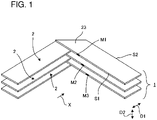
- the flat harness 1 is configured by laminating a plurality of (for example, three) flat circuit bodies 2.
- the plurality of flat circuit bodies 2 are each provided in a long sheet shape, and have substantially the same width.
- each of the flat circuit bodies 2 includes conductive portions 21 and a pair of insulating covering portions 22, 22 that cover both surfaces of each conductive portion 21.
- the conductive portions 21 are each provided in a long sheet shape, and the plurality of conductive portions 21 are arranged side by side at intervals in a width direction D1.
- the pair of insulating covering portions 22, 22 is also provided in a long sheet shape, and covers the plurality of conductive portions 21 with both sides thereof sandwiched in a thickness direction D2.
- the plurality of conductive portions 21 are provided, but the present invention is not limited thereto, and one conductive portion 21 may be provided.
- the flat harness 1 is formed to have a desired harness shape and be guided to a mating connector of an electrical component by appropriately providing a bent portion 23 in which a plane of each flat circuit body 2 is partially overlapped and bent.
- the plane of the flat circuit body 2 described above is a surface facing the thickness direction D2 of the flat circuit body 2.
- each of the flat circuit bodies 2 is provided with the bent portion 23 bent at approximately 90 degrees, and as shown in Fig. 4 , the bent portions 23 are also stacked in the thickness direction D2.
- the flat circuit bodies 2 described above are respectively provided with markings M1 to M3 on one side surface S1 of a pair of side surfaces S1, S2 ( Fig. 1 ) opposite to each other in the width direction D1.
- the markings M1 to M3 are for identifying the flat circuit bodies 2, and are provided by applying ink or the like and coloring.
- the markings M1 to M3 are provided in a vicinity of the bent portions 23 in the side surface S1.
- distances of the flat circuit bodies 2 in a length direction D3 from the respective bent portions 23 (a reference position) to the markings M1 to M3 are provided to be different for each type of the flat circuit bodies 2 provided with the markings M1 to M3.
- the type of the flat circuit body 2 is classified according to a form of the flat circuit body 2 (for example, the number of conductive portions 21) and a shape (a different length, or the like) of the flat circuit body 2.
- the marking M1 provided on the flat circuit body 2 stacked on the top in Fig. 4 is provided such that the distance from the bent portion 23 is shortest.
- the marking M2 provided on the flat circuit body 2 stacked in the middle is provided such that the distance from the bent portion 23 is second shortest.
- the marking M3 provided on the flat circuit body 2 stacked at the bottom is provided such that the distance from the bent portion 23 is the longest. That is, in the plurality of flat circuit bodies 2, the distances from the bent portions 23 to the markings M1 to M3 become longer as arrangement positions of the markings go downward (one side) in the thickness direction D2.
- the markings M1 to M3 are provided on the side surfaces S1 of the flat circuit bodies 2.
- the distances from the respective bent portions 23 to the markings M1 to M3 are different for each type of the flat circuit bodies 2.
- positions of the markings M1 to M3 in the length direction D3 are different for each type of the flat circuit bodies 2. Accordingly, the flat circuit body 2 can be identified by the positions of the markings M1 to M3 in the length direction D3 (the distances from the respective bent portions 23 to the markings M1 to M3). Therefore, the flat circuit body 2 can be easily identified at low cost.
- the markings M1 to M3 are provided by coloring. Accordingly, the markings M1 to M3 can be easily provided. In addition, since the distances from the respective bent portions 23 to the markings M1 to M3 are different for each type of the flat circuit bodies 2, even if the markings M1 to M3 are each provided by coloring on a portion having a small area such as the side surface S1, the flat circuit body 2 can be easily identified.
- the distances from the bent portions 23 to the markings M1 to M3 become longer as the arrangement positions go downward in the thickness direction D2. As a result, it is possible to easily recognize whether or not there is an error in the lamination of the flat circuit body 2.
- the identification jig 10 is provided in a substantially cubic shape, includes a bottom wall (not shown) and three side walls 11 to 13 erecting from the bottom wall, and has an elongated groove portion 14 formed therein. A periphery of the bent portion 23 of the flat harness 1 is inserted into the groove portion 14.
- the side walls 11, 12 are spaced apart from each other in a width direction D4 of the groove portion 14 and form the groove portion 14 therebetween.
- One side (a lower side in the figure) of the groove portion 14 in a depth direction D5 is closed by the bottom wall (not shown), and another side (an upper side in the figure) of the groove portion 14 in the depth direction D5 is opened.
- one side (a right side in the figure) of the groove 14 in a longitudinal direction D6 is opened, and another side (a left side in the figure) of the longitudinal direction D6 is closed by the side wall 13.
- the operator inserts the periphery of the bent portion 23 of the flat harness 1 into the groove portion 14 so that the side surface portion S21 of the flat circuit body 2 abuts against the bottom wall (not shown) of the identification jig 10 and the side surface portion S12 abuts against the side wall 13.
- the markings M1 to M3 provided on the side surface portions S11 of the flat circuit bodies 2 can be visually recognized from an upper opening of the groove portion 14.
- dotted lines L1 to L4 indicating ranges of the markings M1 to M3 provided on the flat circuit bodies 2 are formed side by side in the longitudinal direction D6 on upper surface and inner surfaces of the side walls 11, 12 by printing or the like.
- an area between the dotted line L1 and the dotted line L2 indicate the range of the marking M1
- an area between the dotted line L2 and the dotted line L3 indicate the range of the marking M2
- an area between the dotted line L3 and the dotted line L4 indicate the range of the marking M3.
- a number "01” indicating the laminating order of the flat circuit body 2 in which the marking M1 is formed between the dotted lines L1, L2 is formed by printing or the like.
- a number "02” indicating the laminating order of the flat circuit body 2 in which the marking M2 is formed between the dotted lines L2, L3 is formed.
- a number "03” indicating the laminating order of the flat circuit body 2 in which the marking M3 is formed between the dotted lines L4, L5 is formed.
- each of the flat circuit bodies 2 can be identified more easily using the identification jig 10 as shown in Fig. 5 .
- the present invention is not limited to the embodiment described above, and may be appropriately modified, improved, or the like.
- materials, shapes, dimensions, numbers, arrangement positions or the like of elements in the embodiment described above are optional and not limited as long as the present invention can be achieved.
- the distances between the respective bent portions 23 and the markings M1 to M3 are different for each type of the flat circuit bodies 2, but the present invention is not limited thereto.
- the colors and shapes of the markings M1 to M3 may be different depending on the type of the flat circuit bodies 2. In this case, the colors of the markings M1 to M3 may be different for each form of the flat circuit bodies 2, and the shapes of the markings M1 to M3 may be different for each shape (the different lengths, or the like) of the flat circuit bodies 2.
- the markings M1, M3 having the same color and different shapes are respectively provided in the uppermost flat circuit body 2 and the lowermost flat circuit body 2, and it can be seen at a glance that the markings M1, M3 are of the same form but have different shapes.
- the correct laminating order of the flat circuit body 2 is shown in Fig. 6 , but the present invention is not limited thereto.
- what is shown in Fig. 7 may be the correct laminating order of the flat circuit body 2.
- the laminating order may be determined using the identification jig 10 on which the positions of the numbers "02" and "03" are changed.
- the reference position of the flat circuit body 2 is the bent portion 23, but the present invention is not limited thereto.
- an end portion of the flat circuit body 2 may be set as the reference position.
- a mark (the markings M1 to M3) provided on the side surface S1 of the flat circuit body 2 is provided by coloring, but the present invention is not limited thereto.
- the mark may be provided by cutting out the side surface S1 or by protruding a tab.
Landscapes
- Engineering & Computer Science (AREA)
- Microelectronics & Electronic Packaging (AREA)
- Mechanical Engineering (AREA)
- Structure Of Printed Boards (AREA)
- Insulated Conductors (AREA)
- Electric Cable Installation (AREA)
Claims (5)
- Flacher Kabelbaum (1), der umfasst:eine Vielzahl flacher Schaltkreiskörper (2), die übereinandergestapelt sind,eine Markierung (M1), die an einer Seitenfläche (S1) jedes der Vielzahl flacher Schaltkreiskörper (2) vorhanden ist, wobei jeder der Vielzahl flacher Schaltkreiskörper (2) einen gebogenen Abschnitt (23) aufweist, der durch Biegen und Überlappen eines Teils des entsprechenden flachen Schaltkreiskörpers (2) gebildet wird, die Vielzahl flacher Schaltkreiskörper (2) in einer Dickenrichtung übereinandergestapelt sind, ein Abstand in der Längsrichtung (D3) des flachen Schaltkreiskörpers (2) von einer Bezugsposition (23) des flachen Schaltkreiskörpers (2) zu der Position der Markierung (M1) für jeden Typ des flachen Schaltkreiskörpers (2) verschieden ist, dadurch gekennzeichnet, dass der gebogene Abschnitt (23) die Bezugsposition ist und die Bezugspositionen (23) der Vielzahl flacher Schaltkreiskörper (2) entlang der Dickenrichtung (D2) ausgerichtet sind.
- Flacher Kabelbaum (1) nach Anspruch 1, wobei die Markierung (M1) durch Einfärben erfolgt.
- Flacher Kabelbaum (1) nach Anspruch 2, wobei eine Farbe oder eine Form der Markierung (M1) für jeden Typ des flachen Schaltkreiskörpers (2) verschieden ist.
- Flacher Kabelbaum (1) nach Anspruch 1, wobei die Vielzahl flacher Schaltkreiskörper (2) so übereinandergestapelt sind, dass Abstände von den Bezugspositionen (23) zu den Positionen der Markierungen (M1, M2, M3) bei der Vielzahl flacher Schaltkreiskörper (2) zu einer Seite in einer Stapelrichtung (D2) der Vielzahl flacher Schaltkreiskörper (2) zunehmen.
- Flacher Kabelbaum (1) nach einem der Ansprüche 1 bis 4, wobei die Vielzahl flacher Schaltkreiskörper (2) in einer Stapelrichtung (D2) übereinandergestapelt sind, und sich die Markierung (M1) in der Stapelrichtung (D2) erstreckt.
Applications Claiming Priority (1)
| Application Number | Priority Date | Filing Date | Title |
|---|---|---|---|
| JP2019114882A JP7025378B2 (ja) | 2019-06-20 | 2019-06-20 | フラットハーネス |
Publications (2)
| Publication Number | Publication Date |
|---|---|
| EP3754670A1 EP3754670A1 (de) | 2020-12-23 |
| EP3754670B1 true EP3754670B1 (de) | 2022-08-17 |
Family
ID=70740528
Family Applications (1)
| Application Number | Title | Priority Date | Filing Date |
|---|---|---|---|
| EP20175226.8A Active EP3754670B1 (de) | 2019-06-20 | 2020-05-18 | Flachkabelbaum |
Country Status (4)
| Country | Link |
|---|---|
| US (1) | US11102881B2 (de) |
| EP (1) | EP3754670B1 (de) |
| JP (1) | JP7025378B2 (de) |
| CN (1) | CN112117048B (de) |
Citations (1)
| Publication number | Priority date | Publication date | Assignee | Title |
|---|---|---|---|---|
| JPH1127817A (ja) * | 1997-07-07 | 1999-01-29 | Harness Sogo Gijutsu Kenkyusho:Kk | ワイヤーハーネスの回路識別法 |
Family Cites Families (12)
| Publication number | Priority date | Publication date | Assignee | Title |
|---|---|---|---|---|
| US4636017A (en) * | 1984-06-01 | 1987-01-13 | Harvey Hubbell Incorporated | Flat conductor cable |
| JPH0351863U (de) * | 1989-09-27 | 1991-05-20 | ||
| JPH05242746A (ja) | 1992-02-26 | 1993-09-21 | Furukawa Electric Co Ltd:The | フラットケーブルの製造方法 |
| JP2591330Y2 (ja) * | 1992-08-28 | 1999-03-03 | 三菱電線工業株式会社 | 多層フラットケーブル |
| JPH0664323U (ja) * | 1993-02-19 | 1994-09-09 | 住友電装株式会社 | フラット・ハーネス |
| JPH0623123A (ja) | 1993-06-11 | 1994-02-01 | Ace Denken:Kk | パチンコゲーム機 |
| JPH07176216A (ja) * | 1993-12-20 | 1995-07-14 | Sumitomo Wiring Syst Ltd | フラット・ハーネス |
| JP3694207B2 (ja) | 2000-02-04 | 2005-09-14 | 株式会社オートネットワーク技術研究所 | 端子付きテープ電線の製造方法およびワイヤハーネスの製造方法 |
| JP3649102B2 (ja) * | 2000-08-11 | 2005-05-18 | 住友電装株式会社 | 折曲フラットハーネス |
| JP2003229225A (ja) | 2002-01-31 | 2003-08-15 | Sumitomo Wiring Syst Ltd | コネクタへの電線接続検査方法 |
| PH12012501703A1 (en) * | 2010-03-02 | 2015-05-20 | Yazaki Corp | Wiring harness and manufacturing method thereof |
| US9842823B2 (en) * | 2014-12-29 | 2017-12-12 | Taiwan Semiconductor Manufacturing Co., Ltd. | Chip-stacking apparatus having a transport device configured to transport a chip onto a substrate |
-
2019
- 2019-06-20 JP JP2019114882A patent/JP7025378B2/ja active Active
-
2020
- 2020-05-18 EP EP20175226.8A patent/EP3754670B1/de active Active
- 2020-05-18 CN CN202010420933.1A patent/CN112117048B/zh active Active
- 2020-05-19 US US16/878,559 patent/US11102881B2/en active Active
Patent Citations (1)
| Publication number | Priority date | Publication date | Assignee | Title |
|---|---|---|---|---|
| JPH1127817A (ja) * | 1997-07-07 | 1999-01-29 | Harness Sogo Gijutsu Kenkyusho:Kk | ワイヤーハーネスの回路識別法 |
Also Published As
| Publication number | Publication date |
|---|---|
| US11102881B2 (en) | 2021-08-24 |
| JP7025378B2 (ja) | 2022-02-24 |
| US20200404776A1 (en) | 2020-12-24 |
| CN112117048B (zh) | 2022-02-25 |
| EP3754670A1 (de) | 2020-12-23 |
| JP2021002452A (ja) | 2021-01-07 |
| CN112117048A (zh) | 2020-12-22 |
Similar Documents
| Publication | Publication Date | Title |
|---|---|---|
| US10424892B2 (en) | Holding frame for a plug-type connector | |
| CN208608339U (zh) | 信号传输线路 | |
| US6597578B2 (en) | Electrical connection box | |
| CN103515892B (zh) | 电气连接箱 | |
| GB1580443A (en) | Electrical coil assembly | |
| JPH0955235A (ja) | 電気接続用配線板 | |
| JP6370256B2 (ja) | 蓄電モジュール | |
| JP3149966U (ja) | モジュール式コネクタ | |
| EP3754670B1 (de) | Flachkabelbaum | |
| JP6623833B2 (ja) | 配線モジュール | |
| US9520255B2 (en) | Connection structure of electronic component and terminal metal fittings | |
| EP1617162B1 (de) | Wärmetauscher | |
| JP2002056722A (ja) | フラットハーネス | |
| US6923671B2 (en) | Electric connection box | |
| US6428335B1 (en) | Bus bar with terminal insulator and connector guide therefor | |
| WO2017163995A1 (ja) | 外部接続バスバー保持モジュールおよび電池接続モジュール | |
| CN107735911A (zh) | 接头连接器 | |
| JP7178309B2 (ja) | 被覆電線ユニット | |
| JP2004006218A (ja) | 打ち抜き装置、打ち抜き方法及びフラットケーブル | |
| JP6445891B2 (ja) | ヒューズユニット及びヒューズユニットの製造方法 | |
| JPH04131845U (ja) | カード型ヒユーズ | |
| US11772149B2 (en) | Punching and clinching of metal sheets | |
| KR200218774Y1 (ko) | 골판지 박스 | |
| JP2009032737A (ja) | フレキシブルプリント配線板 | |
| JP7098471B2 (ja) | 端子接続構造、電気接続箱及びワイヤハーネス |
Legal Events
| Date | Code | Title | Description |
|---|---|---|---|
| PUAI | Public reference made under article 153(3) epc to a published international application that has entered the european phase |
Free format text: ORIGINAL CODE: 0009012 |
|
| STAA | Information on the status of an ep patent application or granted ep patent |
Free format text: STATUS: REQUEST FOR EXAMINATION WAS MADE |
|
| 17P | Request for examination filed |
Effective date: 20200518 |
|
| AK | Designated contracting states |
Kind code of ref document: A1 Designated state(s): AL AT BE BG CH CY CZ DE DK EE ES FI FR GB GR HR HU IE IS IT LI LT LU LV MC MK MT NL NO PL PT RO RS SE SI SK SM TR |
|
| AX | Request for extension of the european patent |
Extension state: BA ME |
|
| STAA | Information on the status of an ep patent application or granted ep patent |
Free format text: STATUS: EXAMINATION IS IN PROGRESS |
|
| 17Q | First examination report despatched |
Effective date: 20210504 |
|
| GRAP | Despatch of communication of intention to grant a patent |
Free format text: ORIGINAL CODE: EPIDOSNIGR1 |
|
| STAA | Information on the status of an ep patent application or granted ep patent |
Free format text: STATUS: GRANT OF PATENT IS INTENDED |
|
| INTG | Intention to grant announced |
Effective date: 20220608 |
|
| GRAS | Grant fee paid |
Free format text: ORIGINAL CODE: EPIDOSNIGR3 |
|
| GRAA | (expected) grant |
Free format text: ORIGINAL CODE: 0009210 |
|
| STAA | Information on the status of an ep patent application or granted ep patent |
Free format text: STATUS: THE PATENT HAS BEEN GRANTED |
|
| AK | Designated contracting states |
Kind code of ref document: B1 Designated state(s): AL AT BE BG CH CY CZ DE DK EE ES FI FR GB GR HR HU IE IS IT LI LT LU LV MC MK MT NL NO PL PT RO RS SE SI SK SM TR |
|
| REG | Reference to a national code |
Ref country code: CH Ref legal event code: EP |
|
| REG | Reference to a national code |
Ref country code: DE Ref legal event code: R096 Ref document number: 602020004534 Country of ref document: DE |
|
| REG | Reference to a national code |
Ref country code: IE Ref legal event code: FG4D |
|
| REG | Reference to a national code |
Ref country code: AT Ref legal event code: REF Ref document number: 1512702 Country of ref document: AT Kind code of ref document: T Effective date: 20220915 |
|
| REG | Reference to a national code |
Ref country code: NL Ref legal event code: MP Effective date: 20220817 |
|
| REG | Reference to a national code |
Ref country code: LT Ref legal event code: MG9D |
|
| PG25 | Lapsed in a contracting state [announced via postgrant information from national office to epo] |
Ref country code: SE Free format text: LAPSE BECAUSE OF FAILURE TO SUBMIT A TRANSLATION OF THE DESCRIPTION OR TO PAY THE FEE WITHIN THE PRESCRIBED TIME-LIMIT Effective date: 20220817 Ref country code: RS Free format text: LAPSE BECAUSE OF FAILURE TO SUBMIT A TRANSLATION OF THE DESCRIPTION OR TO PAY THE FEE WITHIN THE PRESCRIBED TIME-LIMIT Effective date: 20220817 Ref country code: PT Free format text: LAPSE BECAUSE OF FAILURE TO SUBMIT A TRANSLATION OF THE DESCRIPTION OR TO PAY THE FEE WITHIN THE PRESCRIBED TIME-LIMIT Effective date: 20221219 Ref country code: NO Free format text: LAPSE BECAUSE OF FAILURE TO SUBMIT A TRANSLATION OF THE DESCRIPTION OR TO PAY THE FEE WITHIN THE PRESCRIBED TIME-LIMIT Effective date: 20221117 Ref country code: NL Free format text: LAPSE BECAUSE OF FAILURE TO SUBMIT A TRANSLATION OF THE DESCRIPTION OR TO PAY THE FEE WITHIN THE PRESCRIBED TIME-LIMIT Effective date: 20220817 Ref country code: LV Free format text: LAPSE BECAUSE OF FAILURE TO SUBMIT A TRANSLATION OF THE DESCRIPTION OR TO PAY THE FEE WITHIN THE PRESCRIBED TIME-LIMIT Effective date: 20220817 Ref country code: LT Free format text: LAPSE BECAUSE OF FAILURE TO SUBMIT A TRANSLATION OF THE DESCRIPTION OR TO PAY THE FEE WITHIN THE PRESCRIBED TIME-LIMIT Effective date: 20220817 Ref country code: FI Free format text: LAPSE BECAUSE OF FAILURE TO SUBMIT A TRANSLATION OF THE DESCRIPTION OR TO PAY THE FEE WITHIN THE PRESCRIBED TIME-LIMIT Effective date: 20220817 |
|
| REG | Reference to a national code |
Ref country code: AT Ref legal event code: MK05 Ref document number: 1512702 Country of ref document: AT Kind code of ref document: T Effective date: 20220817 |
|
| PG25 | Lapsed in a contracting state [announced via postgrant information from national office to epo] |
Ref country code: PL Free format text: LAPSE BECAUSE OF FAILURE TO SUBMIT A TRANSLATION OF THE DESCRIPTION OR TO PAY THE FEE WITHIN THE PRESCRIBED TIME-LIMIT Effective date: 20220817 Ref country code: IS Free format text: LAPSE BECAUSE OF FAILURE TO SUBMIT A TRANSLATION OF THE DESCRIPTION OR TO PAY THE FEE WITHIN THE PRESCRIBED TIME-LIMIT Effective date: 20221217 Ref country code: HR Free format text: LAPSE BECAUSE OF FAILURE TO SUBMIT A TRANSLATION OF THE DESCRIPTION OR TO PAY THE FEE WITHIN THE PRESCRIBED TIME-LIMIT Effective date: 20220817 Ref country code: GR Free format text: LAPSE BECAUSE OF FAILURE TO SUBMIT A TRANSLATION OF THE DESCRIPTION OR TO PAY THE FEE WITHIN THE PRESCRIBED TIME-LIMIT Effective date: 20221118 |
|
| PG25 | Lapsed in a contracting state [announced via postgrant information from national office to epo] |
Ref country code: SM Free format text: LAPSE BECAUSE OF FAILURE TO SUBMIT A TRANSLATION OF THE DESCRIPTION OR TO PAY THE FEE WITHIN THE PRESCRIBED TIME-LIMIT Effective date: 20220817 Ref country code: RO Free format text: LAPSE BECAUSE OF FAILURE TO SUBMIT A TRANSLATION OF THE DESCRIPTION OR TO PAY THE FEE WITHIN THE PRESCRIBED TIME-LIMIT Effective date: 20220817 Ref country code: ES Free format text: LAPSE BECAUSE OF FAILURE TO SUBMIT A TRANSLATION OF THE DESCRIPTION OR TO PAY THE FEE WITHIN THE PRESCRIBED TIME-LIMIT Effective date: 20220817 Ref country code: DK Free format text: LAPSE BECAUSE OF FAILURE TO SUBMIT A TRANSLATION OF THE DESCRIPTION OR TO PAY THE FEE WITHIN THE PRESCRIBED TIME-LIMIT Effective date: 20220817 Ref country code: CZ Free format text: LAPSE BECAUSE OF FAILURE TO SUBMIT A TRANSLATION OF THE DESCRIPTION OR TO PAY THE FEE WITHIN THE PRESCRIBED TIME-LIMIT Effective date: 20220817 Ref country code: AT Free format text: LAPSE BECAUSE OF FAILURE TO SUBMIT A TRANSLATION OF THE DESCRIPTION OR TO PAY THE FEE WITHIN THE PRESCRIBED TIME-LIMIT Effective date: 20220817 |
|
| REG | Reference to a national code |
Ref country code: DE Ref legal event code: R097 Ref document number: 602020004534 Country of ref document: DE |
|
| PG25 | Lapsed in a contracting state [announced via postgrant information from national office to epo] |
Ref country code: SK Free format text: LAPSE BECAUSE OF FAILURE TO SUBMIT A TRANSLATION OF THE DESCRIPTION OR TO PAY THE FEE WITHIN THE PRESCRIBED TIME-LIMIT Effective date: 20220817 Ref country code: EE Free format text: LAPSE BECAUSE OF FAILURE TO SUBMIT A TRANSLATION OF THE DESCRIPTION OR TO PAY THE FEE WITHIN THE PRESCRIBED TIME-LIMIT Effective date: 20220817 |
|
| PLBE | No opposition filed within time limit |
Free format text: ORIGINAL CODE: 0009261 |
|
| STAA | Information on the status of an ep patent application or granted ep patent |
Free format text: STATUS: NO OPPOSITION FILED WITHIN TIME LIMIT |
|
| PG25 | Lapsed in a contracting state [announced via postgrant information from national office to epo] |
Ref country code: AL Free format text: LAPSE BECAUSE OF FAILURE TO SUBMIT A TRANSLATION OF THE DESCRIPTION OR TO PAY THE FEE WITHIN THE PRESCRIBED TIME-LIMIT Effective date: 20220817 |
|
| 26N | No opposition filed |
Effective date: 20230519 |
|
| PG25 | Lapsed in a contracting state [announced via postgrant information from national office to epo] |
Ref country code: SI Free format text: LAPSE BECAUSE OF FAILURE TO SUBMIT A TRANSLATION OF THE DESCRIPTION OR TO PAY THE FEE WITHIN THE PRESCRIBED TIME-LIMIT Effective date: 20220817 |
|
| REG | Reference to a national code |
Ref country code: CH Ref legal event code: PL |
|
| PG25 | Lapsed in a contracting state [announced via postgrant information from national office to epo] |
Ref country code: MC Free format text: LAPSE BECAUSE OF FAILURE TO SUBMIT A TRANSLATION OF THE DESCRIPTION OR TO PAY THE FEE WITHIN THE PRESCRIBED TIME-LIMIT Effective date: 20220817 |
|
| REG | Reference to a national code |
Ref country code: BE Ref legal event code: MM Effective date: 20230531 |
|
| PG25 | Lapsed in a contracting state [announced via postgrant information from national office to epo] |
Ref country code: MC Free format text: LAPSE BECAUSE OF FAILURE TO SUBMIT A TRANSLATION OF THE DESCRIPTION OR TO PAY THE FEE WITHIN THE PRESCRIBED TIME-LIMIT Effective date: 20220817 Ref country code: LU Free format text: LAPSE BECAUSE OF NON-PAYMENT OF DUE FEES Effective date: 20230518 Ref country code: LI Free format text: LAPSE BECAUSE OF NON-PAYMENT OF DUE FEES Effective date: 20230531 Ref country code: CH Free format text: LAPSE BECAUSE OF NON-PAYMENT OF DUE FEES Effective date: 20230531 |
|
| REG | Reference to a national code |
Ref country code: IE Ref legal event code: MM4A |
|
| PG25 | Lapsed in a contracting state [announced via postgrant information from national office to epo] |
Ref country code: IE Free format text: LAPSE BECAUSE OF NON-PAYMENT OF DUE FEES Effective date: 20230518 |
|
| PG25 | Lapsed in a contracting state [announced via postgrant information from national office to epo] |
Ref country code: IE Free format text: LAPSE BECAUSE OF NON-PAYMENT OF DUE FEES Effective date: 20230518 |
|
| PG25 | Lapsed in a contracting state [announced via postgrant information from national office to epo] |
Ref country code: IT Free format text: LAPSE BECAUSE OF FAILURE TO SUBMIT A TRANSLATION OF THE DESCRIPTION OR TO PAY THE FEE WITHIN THE PRESCRIBED TIME-LIMIT Effective date: 20220817 Ref country code: FR Free format text: LAPSE BECAUSE OF NON-PAYMENT OF DUE FEES Effective date: 20230531 Ref country code: BE Free format text: LAPSE BECAUSE OF NON-PAYMENT OF DUE FEES Effective date: 20230531 |
|
| PG25 | Lapsed in a contracting state [announced via postgrant information from national office to epo] |
Ref country code: BG Free format text: LAPSE BECAUSE OF FAILURE TO SUBMIT A TRANSLATION OF THE DESCRIPTION OR TO PAY THE FEE WITHIN THE PRESCRIBED TIME-LIMIT Effective date: 20220817 |
|
| PG25 | Lapsed in a contracting state [announced via postgrant information from national office to epo] |
Ref country code: BG Free format text: LAPSE BECAUSE OF FAILURE TO SUBMIT A TRANSLATION OF THE DESCRIPTION OR TO PAY THE FEE WITHIN THE PRESCRIBED TIME-LIMIT Effective date: 20220817 |
|
| GBPC | Gb: european patent ceased through non-payment of renewal fee |
Effective date: 20240518 |
|
| PG25 | Lapsed in a contracting state [announced via postgrant information from national office to epo] |
Ref country code: GB Free format text: LAPSE BECAUSE OF NON-PAYMENT OF DUE FEES Effective date: 20240518 |
|
| PGFP | Annual fee paid to national office [announced via postgrant information from national office to epo] |
Ref country code: DE Payment date: 20250402 Year of fee payment: 6 |
|
| PG25 | Lapsed in a contracting state [announced via postgrant information from national office to epo] |
Ref country code: CY Free format text: LAPSE BECAUSE OF FAILURE TO SUBMIT A TRANSLATION OF THE DESCRIPTION OR TO PAY THE FEE WITHIN THE PRESCRIBED TIME-LIMIT; INVALID AB INITIO Effective date: 20200518 |
|
| PG25 | Lapsed in a contracting state [announced via postgrant information from national office to epo] |
Ref country code: HU Free format text: LAPSE BECAUSE OF FAILURE TO SUBMIT A TRANSLATION OF THE DESCRIPTION OR TO PAY THE FEE WITHIN THE PRESCRIBED TIME-LIMIT; INVALID AB INITIO Effective date: 20200518 |
|
| PG25 | Lapsed in a contracting state [announced via postgrant information from national office to epo] |
Ref country code: TR Free format text: LAPSE BECAUSE OF FAILURE TO SUBMIT A TRANSLATION OF THE DESCRIPTION OR TO PAY THE FEE WITHIN THE PRESCRIBED TIME-LIMIT Effective date: 20220817 |