EP3753045B1 - Verfahren zur herstellung von verbindungen mit niedriger schmelztemperatur auf wafer-ebene für eine wafer-bonding-anordnung - Google Patents
Verfahren zur herstellung von verbindungen mit niedriger schmelztemperatur auf wafer-ebene für eine wafer-bonding-anordnung Download PDFInfo
- Publication number
- EP3753045B1 EP3753045B1 EP18773680.6A EP18773680A EP3753045B1 EP 3753045 B1 EP3753045 B1 EP 3753045B1 EP 18773680 A EP18773680 A EP 18773680A EP 3753045 B1 EP3753045 B1 EP 3753045B1
- Authority
- EP
- European Patent Office
- Prior art keywords
- posts
- wafer
- layer
- array
- degrees celsius
- Prior art date
- Legal status (The legal status is an assumption and is not a legal conclusion. Google has not performed a legal analysis and makes no representation as to the accuracy of the status listed.)
- Active
Links
Images



Classifications
-
- H—ELECTRICITY
- H10—SEMICONDUCTOR DEVICES; ELECTRIC SOLID-STATE DEVICES NOT OTHERWISE PROVIDED FOR
- H10W—GENERIC PACKAGES, INTERCONNECTIONS, CONNECTORS OR OTHER CONSTRUCTIONAL DETAILS OF DEVICES COVERED BY CLASS H10
- H10W20/00—Interconnections in chips, wafers or substrates
- H10W20/01—Manufacture or treatment
- H10W20/031—Manufacture or treatment of conductive parts of the interconnections
- H10W20/062—Manufacture or treatment of conductive parts of the interconnections by smoothing of conductive parts, e.g. by planarisation
-
- C—CHEMISTRY; METALLURGY
- C23—COATING METALLIC MATERIAL; COATING MATERIAL WITH METALLIC MATERIAL; CHEMICAL SURFACE TREATMENT; DIFFUSION TREATMENT OF METALLIC MATERIAL; COATING BY VACUUM EVAPORATION, BY SPUTTERING, BY ION IMPLANTATION OR BY CHEMICAL VAPOUR DEPOSITION, IN GENERAL; INHIBITING CORROSION OF METALLIC MATERIAL OR INCRUSTATION IN GENERAL
- C23C—COATING METALLIC MATERIAL; COATING MATERIAL WITH METALLIC MATERIAL; SURFACE TREATMENT OF METALLIC MATERIAL BY DIFFUSION INTO THE SURFACE, BY CHEMICAL CONVERSION OR SUBSTITUTION; COATING BY VACUUM EVAPORATION, BY SPUTTERING, BY ION IMPLANTATION OR BY CHEMICAL VAPOUR DEPOSITION, IN GENERAL
- C23C18/00—Chemical coating by decomposition of either liquid compounds or solutions of the coating forming compounds, without leaving reaction products of surface material in the coating; Contact plating
- C23C18/16—Chemical coating by decomposition of either liquid compounds or solutions of the coating forming compounds, without leaving reaction products of surface material in the coating; Contact plating by reduction or substitution, e.g. electroless plating
- C23C18/1601—Process or apparatus
- C23C18/1633—Process of electroless plating
- C23C18/1646—Characteristics of the product obtained
- C23C18/165—Multilayered product
- C23C18/1653—Two or more layers with at least one layer obtained by electroless plating and one layer obtained by electroplating
-
- C—CHEMISTRY; METALLURGY
- C23—COATING METALLIC MATERIAL; COATING MATERIAL WITH METALLIC MATERIAL; CHEMICAL SURFACE TREATMENT; DIFFUSION TREATMENT OF METALLIC MATERIAL; COATING BY VACUUM EVAPORATION, BY SPUTTERING, BY ION IMPLANTATION OR BY CHEMICAL VAPOUR DEPOSITION, IN GENERAL; INHIBITING CORROSION OF METALLIC MATERIAL OR INCRUSTATION IN GENERAL
- C23C—COATING METALLIC MATERIAL; COATING MATERIAL WITH METALLIC MATERIAL; SURFACE TREATMENT OF METALLIC MATERIAL BY DIFFUSION INTO THE SURFACE, BY CHEMICAL CONVERSION OR SUBSTITUTION; COATING BY VACUUM EVAPORATION, BY SPUTTERING, BY ION IMPLANTATION OR BY CHEMICAL VAPOUR DEPOSITION, IN GENERAL
- C23C18/00—Chemical coating by decomposition of either liquid compounds or solutions of the coating forming compounds, without leaving reaction products of surface material in the coating; Contact plating
- C23C18/16—Chemical coating by decomposition of either liquid compounds or solutions of the coating forming compounds, without leaving reaction products of surface material in the coating; Contact plating by reduction or substitution, e.g. electroless plating
- C23C18/1601—Process or apparatus
- C23C18/1633—Process of electroless plating
- C23C18/1675—Process conditions
- C23C18/168—Control of temperature, e.g. temperature of bath, substrate
-
- C—CHEMISTRY; METALLURGY
- C25—ELECTROLYTIC OR ELECTROPHORETIC PROCESSES; APPARATUS THEREFOR
- C25D—PROCESSES FOR THE ELECTROLYTIC OR ELECTROPHORETIC PRODUCTION OF COATINGS; ELECTROFORMING; APPARATUS THEREFOR
- C25D7/00—Electroplating characterised by the article coated
- C25D7/12—Semiconductors
- C25D7/123—Semiconductors first coated with a seed layer or a conductive layer
-
- H—ELECTRICITY
- H05—ELECTRIC TECHNIQUES NOT OTHERWISE PROVIDED FOR
- H05K—PRINTED CIRCUITS; CASINGS OR CONSTRUCTIONAL DETAILS OF ELECTRIC APPARATUS; MANUFACTURE OF ASSEMBLAGES OF ELECTRICAL COMPONENTS
- H05K3/00—Apparatus or processes for manufacturing printed circuits
- H05K3/40—Forming printed elements for providing electric connections to or between printed circuits
- H05K3/42—Plated through-holes or plated via connections
- H05K3/423—Plated through-holes or plated via connections characterised by electroplating method
- H05K3/424—Plated through-holes or plated via connections characterised by electroplating method by direct electroplating
-
- H—ELECTRICITY
- H10—SEMICONDUCTOR DEVICES; ELECTRIC SOLID-STATE DEVICES NOT OTHERWISE PROVIDED FOR
- H10P—GENERIC PROCESSES OR APPARATUS FOR THE MANUFACTURE OR TREATMENT OF DEVICES COVERED BY CLASS H10
- H10P70/00—Cleaning of wafers, substrates or parts of devices
- H10P70/20—Cleaning during device manufacture
- H10P70/23—Cleaning during device manufacture during, before or after processing of insulating materials
- H10P70/237—Cleaning during device manufacture during, before or after processing of insulating materials the processing being a planarisation of insulating layers
-
- H—ELECTRICITY
- H10—SEMICONDUCTOR DEVICES; ELECTRIC SOLID-STATE DEVICES NOT OTHERWISE PROVIDED FOR
- H10W—GENERIC PACKAGES, INTERCONNECTIONS, CONNECTORS OR OTHER CONSTRUCTIONAL DETAILS OF DEVICES COVERED BY CLASS H10
- H10W20/00—Interconnections in chips, wafers or substrates
- H10W20/01—Manufacture or treatment
- H10W20/031—Manufacture or treatment of conductive parts of the interconnections
- H10W20/032—Manufacture or treatment of conductive parts of the interconnections of conductive barrier, adhesion or liner layers
- H10W20/042—Manufacture or treatment of conductive parts of the interconnections of conductive barrier, adhesion or liner layers the barrier, adhesion or liner layers being seed or nucleation layers
- H10W20/043—Manufacture or treatment of conductive parts of the interconnections of conductive barrier, adhesion or liner layers the barrier, adhesion or liner layers being seed or nucleation layers for electroplating
-
- H—ELECTRICITY
- H10—SEMICONDUCTOR DEVICES; ELECTRIC SOLID-STATE DEVICES NOT OTHERWISE PROVIDED FOR
- H10W—GENERIC PACKAGES, INTERCONNECTIONS, CONNECTORS OR OTHER CONSTRUCTIONAL DETAILS OF DEVICES COVERED BY CLASS H10
- H10W20/00—Interconnections in chips, wafers or substrates
- H10W20/40—Interconnections external to wafers or substrates, e.g. back-end-of-line [BEOL] metallisations or vias connecting to gate electrodes
- H10W20/41—Interconnections external to wafers or substrates, e.g. back-end-of-line [BEOL] metallisations or vias connecting to gate electrodes characterised by their conductive parts
- H10W20/435—Cross-sectional shapes or dispositions of interconnections
-
- H—ELECTRICITY
- H10—SEMICONDUCTOR DEVICES; ELECTRIC SOLID-STATE DEVICES NOT OTHERWISE PROVIDED FOR
- H10W—GENERIC PACKAGES, INTERCONNECTIONS, CONNECTORS OR OTHER CONSTRUCTIONAL DETAILS OF DEVICES COVERED BY CLASS H10
- H10W72/00—Interconnections or connectors in packages
- H10W72/20—Bump connectors, e.g. solder bumps or copper pillars; Dummy bumps; Thermal bumps
-
- H—ELECTRICITY
- H10—SEMICONDUCTOR DEVICES; ELECTRIC SOLID-STATE DEVICES NOT OTHERWISE PROVIDED FOR
- H10W—GENERIC PACKAGES, INTERCONNECTIONS, CONNECTORS OR OTHER CONSTRUCTIONAL DETAILS OF DEVICES COVERED BY CLASS H10
- H10W72/00—Interconnections or connectors in packages
- H10W72/90—Bond pads, in general
-
- H—ELECTRICITY
- H10—SEMICONDUCTOR DEVICES; ELECTRIC SOLID-STATE DEVICES NOT OTHERWISE PROVIDED FOR
- H10W—GENERIC PACKAGES, INTERCONNECTIONS, CONNECTORS OR OTHER CONSTRUCTIONAL DETAILS OF DEVICES COVERED BY CLASS H10
- H10W74/00—Encapsulations, e.g. protective coatings
- H10W74/01—Manufacture or treatment
- H10W74/019—Manufacture or treatment using temporary auxiliary substrates
-
- H—ELECTRICITY
- H10—SEMICONDUCTOR DEVICES; ELECTRIC SOLID-STATE DEVICES NOT OTHERWISE PROVIDED FOR
- H10W—GENERIC PACKAGES, INTERCONNECTIONS, CONNECTORS OR OTHER CONSTRUCTIONAL DETAILS OF DEVICES COVERED BY CLASS H10
- H10W74/00—Encapsulations, e.g. protective coatings
- H10W74/10—Encapsulations, e.g. protective coatings characterised by their shape or disposition
- H10W74/111—Encapsulations, e.g. protective coatings characterised by their shape or disposition the semiconductor body being completely enclosed
- H10W74/114—Encapsulations, e.g. protective coatings characterised by their shape or disposition the semiconductor body being completely enclosed by a substrate and the encapsulations
-
- H—ELECTRICITY
- H10—SEMICONDUCTOR DEVICES; ELECTRIC SOLID-STATE DEVICES NOT OTHERWISE PROVIDED FOR
- H10W—GENERIC PACKAGES, INTERCONNECTIONS, CONNECTORS OR OTHER CONSTRUCTIONAL DETAILS OF DEVICES COVERED BY CLASS H10
- H10W20/00—Interconnections in chips, wafers or substrates
- H10W20/01—Manufacture or treatment
- H10W20/031—Manufacture or treatment of conductive parts of the interconnections
- H10W20/032—Manufacture or treatment of conductive parts of the interconnections of conductive barrier, adhesion or liner layers
- H10W20/042—Manufacture or treatment of conductive parts of the interconnections of conductive barrier, adhesion or liner layers the barrier, adhesion or liner layers being seed or nucleation layers
- H10W20/0425—Manufacture or treatment of conductive parts of the interconnections of conductive barrier, adhesion or liner layers the barrier, adhesion or liner layers being seed or nucleation layers comprising multiple stacked seed or nucleation layers
-
- H—ELECTRICITY
- H10—SEMICONDUCTOR DEVICES; ELECTRIC SOLID-STATE DEVICES NOT OTHERWISE PROVIDED FOR
- H10W—GENERIC PACKAGES, INTERCONNECTIONS, CONNECTORS OR OTHER CONSTRUCTIONAL DETAILS OF DEVICES COVERED BY CLASS H10
- H10W72/00—Interconnections or connectors in packages
- H10W72/01—Manufacture or treatment
- H10W72/019—Manufacture or treatment of bond pads
-
- H—ELECTRICITY
- H10—SEMICONDUCTOR DEVICES; ELECTRIC SOLID-STATE DEVICES NOT OTHERWISE PROVIDED FOR
- H10W—GENERIC PACKAGES, INTERCONNECTIONS, CONNECTORS OR OTHER CONSTRUCTIONAL DETAILS OF DEVICES COVERED BY CLASS H10
- H10W72/00—Interconnections or connectors in packages
- H10W72/01—Manufacture or treatment
- H10W72/019—Manufacture or treatment of bond pads
- H10W72/01904—Manufacture or treatment of bond pads using temporary auxiliary members, e.g. using sacrificial coatings or handle substrates
-
- H—ELECTRICITY
- H10—SEMICONDUCTOR DEVICES; ELECTRIC SOLID-STATE DEVICES NOT OTHERWISE PROVIDED FOR
- H10W—GENERIC PACKAGES, INTERCONNECTIONS, CONNECTORS OR OTHER CONSTRUCTIONAL DETAILS OF DEVICES COVERED BY CLASS H10
- H10W72/00—Interconnections or connectors in packages
- H10W72/01—Manufacture or treatment
- H10W72/019—Manufacture or treatment of bond pads
- H10W72/01931—Manufacture or treatment of bond pads using blanket deposition
- H10W72/01933—Manufacture or treatment of bond pads using blanket deposition in liquid form, e.g. spin coating, spray coating or immersion coating
- H10W72/01935—Manufacture or treatment of bond pads using blanket deposition in liquid form, e.g. spin coating, spray coating or immersion coating by plating, e.g. electroless plating or electroplating
-
- H—ELECTRICITY
- H10—SEMICONDUCTOR DEVICES; ELECTRIC SOLID-STATE DEVICES NOT OTHERWISE PROVIDED FOR
- H10W—GENERIC PACKAGES, INTERCONNECTIONS, CONNECTORS OR OTHER CONSTRUCTIONAL DETAILS OF DEVICES COVERED BY CLASS H10
- H10W72/00—Interconnections or connectors in packages
- H10W72/01—Manufacture or treatment
- H10W72/019—Manufacture or treatment of bond pads
- H10W72/01931—Manufacture or treatment of bond pads using blanket deposition
- H10W72/01938—Manufacture or treatment of bond pads using blanket deposition in gaseous form, e.g. by CVD or PVD
-
- H—ELECTRICITY
- H10—SEMICONDUCTOR DEVICES; ELECTRIC SOLID-STATE DEVICES NOT OTHERWISE PROVIDED FOR
- H10W—GENERIC PACKAGES, INTERCONNECTIONS, CONNECTORS OR OTHER CONSTRUCTIONAL DETAILS OF DEVICES COVERED BY CLASS H10
- H10W72/00—Interconnections or connectors in packages
- H10W72/01—Manufacture or treatment
- H10W72/019—Manufacture or treatment of bond pads
- H10W72/01951—Changing the shapes of bond pads
-
- H—ELECTRICITY
- H10—SEMICONDUCTOR DEVICES; ELECTRIC SOLID-STATE DEVICES NOT OTHERWISE PROVIDED FOR
- H10W—GENERIC PACKAGES, INTERCONNECTIONS, CONNECTORS OR OTHER CONSTRUCTIONAL DETAILS OF DEVICES COVERED BY CLASS H10
- H10W72/00—Interconnections or connectors in packages
- H10W72/01—Manufacture or treatment
- H10W72/019—Manufacture or treatment of bond pads
- H10W72/01951—Changing the shapes of bond pads
- H10W72/01953—Changing the shapes of bond pads by etching
-
- H—ELECTRICITY
- H10—SEMICONDUCTOR DEVICES; ELECTRIC SOLID-STATE DEVICES NOT OTHERWISE PROVIDED FOR
- H10W—GENERIC PACKAGES, INTERCONNECTIONS, CONNECTORS OR OTHER CONSTRUCTIONAL DETAILS OF DEVICES COVERED BY CLASS H10
- H10W72/00—Interconnections or connectors in packages
- H10W72/01—Manufacture or treatment
- H10W72/019—Manufacture or treatment of bond pads
- H10W72/01951—Changing the shapes of bond pads
- H10W72/01955—Changing the shapes of bond pads by using masks
-
- H—ELECTRICITY
- H10—SEMICONDUCTOR DEVICES; ELECTRIC SOLID-STATE DEVICES NOT OTHERWISE PROVIDED FOR
- H10W—GENERIC PACKAGES, INTERCONNECTIONS, CONNECTORS OR OTHER CONSTRUCTIONAL DETAILS OF DEVICES COVERED BY CLASS H10
- H10W72/00—Interconnections or connectors in packages
- H10W72/01—Manufacture or treatment
- H10W72/0198—Manufacture or treatment batch processes
-
- H—ELECTRICITY
- H10—SEMICONDUCTOR DEVICES; ELECTRIC SOLID-STATE DEVICES NOT OTHERWISE PROVIDED FOR
- H10W—GENERIC PACKAGES, INTERCONNECTIONS, CONNECTORS OR OTHER CONSTRUCTIONAL DETAILS OF DEVICES COVERED BY CLASS H10
- H10W72/00—Interconnections or connectors in packages
- H10W72/071—Connecting or disconnecting
- H10W72/073—Connecting or disconnecting of die-attach connectors
- H10W72/07331—Connecting techniques
-
- H—ELECTRICITY
- H10—SEMICONDUCTOR DEVICES; ELECTRIC SOLID-STATE DEVICES NOT OTHERWISE PROVIDED FOR
- H10W—GENERIC PACKAGES, INTERCONNECTIONS, CONNECTORS OR OTHER CONSTRUCTIONAL DETAILS OF DEVICES COVERED BY CLASS H10
- H10W72/00—Interconnections or connectors in packages
- H10W72/90—Bond pads, in general
- H10W72/941—Dispositions of bond pads
-
- H—ELECTRICITY
- H10—SEMICONDUCTOR DEVICES; ELECTRIC SOLID-STATE DEVICES NOT OTHERWISE PROVIDED FOR
- H10W—GENERIC PACKAGES, INTERCONNECTIONS, CONNECTORS OR OTHER CONSTRUCTIONAL DETAILS OF DEVICES COVERED BY CLASS H10
- H10W72/00—Interconnections or connectors in packages
- H10W72/90—Bond pads, in general
- H10W72/951—Materials of bond pads
- H10W72/952—Materials of bond pads comprising metals or metalloids, e.g. PbSn, Ag or Cu
-
- H—ELECTRICITY
- H10—SEMICONDUCTOR DEVICES; ELECTRIC SOLID-STATE DEVICES NOT OTHERWISE PROVIDED FOR
- H10W—GENERIC PACKAGES, INTERCONNECTIONS, CONNECTORS OR OTHER CONSTRUCTIONAL DETAILS OF DEVICES COVERED BY CLASS H10
- H10W80/00—Direct bonding of chips, wafers or substrates
- H10W80/011—Manufacture or treatment of pads or other interconnections to be direct bonded
- H10W80/016—Cleaning
-
- H—ELECTRICITY
- H10—SEMICONDUCTOR DEVICES; ELECTRIC SOLID-STATE DEVICES NOT OTHERWISE PROVIDED FOR
- H10W—GENERIC PACKAGES, INTERCONNECTIONS, CONNECTORS OR OTHER CONSTRUCTIONAL DETAILS OF DEVICES COVERED BY CLASS H10
- H10W80/00—Direct bonding of chips, wafers or substrates
- H10W80/011—Manufacture or treatment of pads or other interconnections to be direct bonded
- H10W80/031—Changing or setting shapes of the pads
-
- H—ELECTRICITY
- H10—SEMICONDUCTOR DEVICES; ELECTRIC SOLID-STATE DEVICES NOT OTHERWISE PROVIDED FOR
- H10W—GENERIC PACKAGES, INTERCONNECTIONS, CONNECTORS OR OTHER CONSTRUCTIONAL DETAILS OF DEVICES COVERED BY CLASS H10
- H10W80/00—Direct bonding of chips, wafers or substrates
- H10W80/011—Manufacture or treatment of pads or other interconnections to be direct bonded
- H10W80/031—Changing or setting shapes of the pads
- H10W80/037—Changing or setting shapes of the pads by mechanical treatment, e.g. by cutting, pressing or stamping
-
- H—ELECTRICITY
- H10—SEMICONDUCTOR DEVICES; ELECTRIC SOLID-STATE DEVICES NOT OTHERWISE PROVIDED FOR
- H10W—GENERIC PACKAGES, INTERCONNECTIONS, CONNECTORS OR OTHER CONSTRUCTIONAL DETAILS OF DEVICES COVERED BY CLASS H10
- H10W80/00—Direct bonding of chips, wafers or substrates
- H10W80/301—Bonding techniques, e.g. hybrid bonding
- H10W80/312—Bonding techniques, e.g. hybrid bonding characterised by the direct bonding of electrically conductive pads
-
- H—ELECTRICITY
- H10—SEMICONDUCTOR DEVICES; ELECTRIC SOLID-STATE DEVICES NOT OTHERWISE PROVIDED FOR
- H10W—GENERIC PACKAGES, INTERCONNECTIONS, CONNECTORS OR OTHER CONSTRUCTIONAL DETAILS OF DEVICES COVERED BY CLASS H10
- H10W80/00—Direct bonding of chips, wafers or substrates
- H10W80/301—Bonding techniques, e.g. hybrid bonding
- H10W80/327—Bonding techniques, e.g. hybrid bonding characterised by the direct bonding of insulating parts, e.g. of silicon oxide layers
-
- H—ELECTRICITY
- H10—SEMICONDUCTOR DEVICES; ELECTRIC SOLID-STATE DEVICES NOT OTHERWISE PROVIDED FOR
- H10W—GENERIC PACKAGES, INTERCONNECTIONS, CONNECTORS OR OTHER CONSTRUCTIONAL DETAILS OF DEVICES COVERED BY CLASS H10
- H10W90/00—Package configurations
- H10W90/701—Package configurations characterised by the relative positions of pads or connectors relative to package parts
- H10W90/791—Package configurations characterised by the relative positions of pads or connectors relative to package parts of direct-bonded pads
- H10W90/792—Package configurations characterised by the relative positions of pads or connectors relative to package parts of direct-bonded pads between multiple chips
Definitions
- the subject disclosure relates to the fabrication of semiconductor devices and more particularly to creating wafer interconnections.
- Typical wafer bonding processes involve connecting wafers using direct bond hybridization (DBH or Direct Bond Interconnection). This involves first forming posts on two wafers by electroplating on a metal seed layer through a plating mold of patterned photoresist (PR). A layer of SiO2 is then deposited over the metal structure. The surfaces are then planarized (i.e. made planar), for example, by using a chemical-mechanical polishing (CMP) process. The planar surfaces of the wafers are then aligned and bonded together and annealed.
- DBH direct bond hybridization
- PR patterned photoresist
- CMP chemical-mechanical polishing
- Certain metals with low melting points such as Indium have desirable attributes when used as interconnections, particularly in processes requiring a compliant interconnection metal and as a non-magnetic metal.
- typical DBH interconnection manufacturing processes tend to exceed a temperature of 225 degrees Celsius. Processes at such high temperatures tend to cause low melting point metals, such as Indium which has a melting point of roughly 157 degrees Celsius, to melt and/or deform prior to interconnection.
- applying CMP on a surface which includes certain low melting point interconnections can contaminate the oxide bonding surface, rendering the surface incapable of the bond strength needed for DBH.
- US 2006/0292851 A1 discloses a circuit structure including a semiconductor substrate, first and second metallic posts over the semiconductor substrate, an insulating layer over the semiconductor substrate and covering the first and second metallic posts, first and second bumps over the first and second metallic posts or over the insulating layer.
- the first and second metallic posts have a height of between 20 and 300 microns, with the ratio of the maximum horizontal dimension thereof to the height thereof being less than 4.
- the distance between the center of the first bump and the center of the second bump is between 10 and 250 microns.
- US 2002/0004288 8 A1 discloses a method of manufacturing LSI chips, comprising the steps of: pasting on a substrate an adhesive sheet which retains its adhesive strength prior to a processing, then loses it after the processing; bonding non-defective LSI chips on the adhesive sheet, with their device surfaces facing downward; uniformly coating an insulating film on the non-defective LSI chips; uniformly grinding the insulating film to a level of the bottom surfaces of these LSI chips; applying a predetermined process to the adhesive sheet to weaken its adhesive strength thereof so as to peel off a pseudo wafer on which the non-defective LSI chips are bonded; and dicing the LSI chips into a discrete non-defective electronic component by cutting the pseudo wafer.
- US 2017/0271217 A1 discloses systems and methods of in-situ calibration of semiconductor material layer deposition and Removal processes are disclosed.
- Sets of test structures including one or more calibration vias or posts are used to precisely monitor processes such as plating and polishing, respectively.
- Known (e.g., empirically determined) relationships between the test structure features and product feature enable monitoring of wafer processing progress.
- Optical inspection of the calibration feature(s) during processing cycles permits dynamic operating condition adjustments and precise cessation of processing when desired product feature characteristics have been achieved.
- XIE LING ET AL "6um Pitch High Density Cu-Cu Bonding for 3D IC Stacking" discloses designing and fabricating a test vehicle with copper pillars having 3 ⁇ m diameter and 6 ⁇ m pitch on a wafer .
- US 2014/0361431 A1 discloses a semiconductor device including a first semiconductor electronic component which includes a pad electrode, a solder bump, and a metal layer between a pad and solder that is configured to have an underlying metal layer formed between the pad electrode and the solder bump and connected to the pad electrode, and a main metal layer formed on the underlying metal layer, and in which the main metal layer has an eave portion at an outer edge portion thereof.
- US 2010/0117227 A1 discloses a method of preparing detectors for oxide bonding to an integrated hip, .e.g, a readout integrated chip, includes providing a wafer having a plurality of detector elements with bumps thereon.
- US 2014/0263959 A1 discloses a device having a sensor die with a sensor and a control circuit die with at least one control circuit disposed therein, the control circuit die on the sensor die.
- the subject technology relates to a method of manufacturing an array of planar wafer level metal posts comprising: providing, a metal seed layer for plating posts or interconnections on a substrate of a first wafer; applying a photoresist, PR, pattern mold over the metal seed layer; plating an array of posts within a photoresist 'PR' pattern mold on the metal seed layer; stripping the PR pattern mold from the substrate and array of posts; after the step of stripping the PR pattern mold, applying a PR layer around each of the posts; after the step of applying a PR layer, etching the metal seed layer on the substrate to isolate the posts from one another; after the step of etching the metal seed layer, stripping the PR layer; applying an oxide layer, at a temperature of below 150 degrees Celsius and below a melting point of the array of posts, over a surface of the first wafer and around the array of posts extending from the surface; applying chemical-mechanical polishing 'CMP' to planarize the oxide layer and the array of posts; after the step
- the oxide layer is applied at a temperature of between 127 degrees Celsius and 147 degrees Celsius. In some cases, the oxide layer is applied at a temperature of between 135 degrees Celsius and 139 degrees Celsius. In some cases, the posts are comprised of Indium.
- the subject technology relates to a method of manufacturing a bonded wafer assembly with Indium interconnections comprising: a) providing a first wafer with a substrate layer, an insulating layer, and a metal seed layer, the metal seed layer connected to the substrate layer by vias extending through a first plurality of holes in the insulating layer; b) applying a photoresist 'PR' pattern mold over the metal seed layer such that a second plurality of holes through the PR pattern mold align with the vias; c) plating Indium within the second plurality of holes in the PR pattern mold to form an array of Indium posts on the first wafer; d) stripping the PR pattern mold; e) etching a portion of the metal seed layer to singulate the array of Indium posts; f) applying an oxide layer, at a temperature below 150 degrees Celsius, over a surface of the first wafer; g) applying chemical-mechanical polishing 'CMP' to form a planar surface, the planar surface including the array of
- the bonding is done through a low temperature annealing process.
- a PR layer is placed around each of the Indium posts. After etching the metal seed layer and before applying the oxide layer the PR layer is stripped.
- a second PR layer is placed over exposed surfaces of the array of Indium posts. After the step of placing a second PR layer an exposed surface of the oxide layer is cleaned. Cleaning an exposed surface of the oxide layer can be done by applying HCl.
- the oxide layer is applied at a temperature of between 127 degrees Celsius and 147 degrees Celsius. In some embodiments, the oxide layer is applied at a temperature of between 135 degrees Celsius and 139 degrees Celsius.
- an "upper" surface of a part is merely meant to describe a surface that is separate from the “lower” surface of that same part, as shown in the figures.
- No words denoting orientation are used to describe an absolute orientation (i.e. where an "upper” part must always be on top).
- the method 100 generally involves creating interconnections on a wafer device such as a III-V semiconductor device and optionally bonding with a separate wafer to form a wafer assembly.
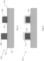
- the method 100 starts at first step 102 which includes providing a first wafer 250 with a device layer 252, an insulating layer 254, and a metal seed layer 256, as seen in FIG. 2 .
- Preliminary steps of manufacturing the first wafer 250 are understood in the art and therefore a thorough description thereof is omitted.
- the device layer 252 is typically a Silicon substrate and includes processing circuitry extending therethrough comprised of Al, Cu, implantation or the like.
- the insulating layer 254 is positioned over the upper surface 260 of the device layer 252 and can be comprised of materials such as SiO 2 , SiN x , or the like.
- the metal seed layer 256 is provided for plating posts or interconnections, as is discussed more fully below, and is comprised of materials such as TiW, Al, Sn, or the like.
- the insulating layer 254 is broken by a first plurality of holes or perforations 262 through which the metal seed layer 256 extends, forming vias 264.
- the vias 264 are used to provide a connection between the device layer 252 and the posts or interconnections discussed below.
- both the insulating layer 254 and the metal seed layer 256 may additionally or alternatively be comprised of other materials known in the art to function in accordance with the insulating layer 254 and metal seed layer 256 described herein
- a photoresist (PR) pattern mold 268 is applied over the metal seed layer 256.
- the PR pattern mold 268 is patterned with a second plurality of holes or perforations 270 which correspond to the perforations 262 in the insulating layer 254.
- the Indium is plated within the PR pattern mold 268 to form an array of posts 266.
- the PR pattern mold 268 allows for improved Indium plating uniformity and reduces Indium contamination from bonding oxide, as the Indium is not dragged across oxide.
- the posts 266 are formed as a small dense array that grows from the metal seed layer 256 when current is provided and will eventually serve as high yield fine pitch array for interconnections for the first wafer 250.
- the posts 266 are grown within the perforations 270 which align with the vias 264, such that the vias 264 connect the posts 266 to the device layer 252. Thus, the posts 266 eventually form the interconnections on the first wafer 250. While Indium has been found to be effectively used to form the posts 266 within the disclosed method 100, it should be noted that the methods discussed herein are applicable to other elements and/or materials which can be used in the formation of wafer interconnections.
- the method 100 and other methods discussed herein have been found to be effective when the posts 266 which form the interconnections are comprised materials/elements with a low melting point, such as below 200 degrees Celsius. This is because the method 100 is designed to avoid melting material with a low melting point, whereas other process of forming interconnections and bonding wafers will often melt and/or deform such material.
- the PR pattern mold 268 is stripped as seen in FIG. 4 .
- a second PR layer 272 is placed surrounding the posts 266 at step 109.
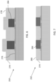
- the metal seed layer 256 is then etched to singulate the posts 266 such that the posts 266 are isolated from one another (i.e. not directly connected through the metal seed layer 256). Etching can be accomplished, for example, by photolithographic techniques as are known in the art.
- the second PR layer 272 protects the posts 266 during the metal etching process and can be stripped, at step 111, after the etching process is complete.
- a low temperature oxide is applied over a surface 276 of the first wafer 250 (and around the posts 266 extending from the surface 276) as seen in FIG. 6 , to form an oxide layer 274.
- the low temperature oxide is below the melting temperature of Indium, which is about 157 degrees Celsius. Therefore, the temperature of the low temperature oxide is applied at a temperature of below 150 degrees Celsius. In some embodiments, the low temperature oxide is applied at a temperature of substantially 20 degrees Celsius below the melting point of Indium, such as between 127 degrees Celsius and 147 degrees Celsius. In other embodiments, the temperature of the low temperature oxide is between 135 degrees Celsius and 139 degrees Celsius.
- corresponding oxide temperature ranges can be applied (e.g. substantially 20 degrees below a melting point of the other material).
- the oxide can be applied within one of the temperature ranges described above.
- a new surface 278 of the first wafer 250 is formed which is typically non-uniform. Therefore at step 114, and as seen in FIG. 7 , chemical-mechanical polishing (CMP) is then applied to the non-uniform surface 278. Applying CMP to the non-uniform surface 278 of the first wafer 250 removes excess post 266 and oxide layer 274 material to smooth and/or level the surface 278. CMP is applied until the oxide layer 274 and posts 266 have been planarized, forming a flat and continuous upper surface 280 of the wafer 250. A planarized surface 280 helps bond the first wafer 250 to a second wafer, as discussed below.
- CMP chemical-mechanical polishing
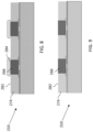
- FIG. 8 shows an intermediate step of placing a second PR layer 284 over the posts 266 to serve as a protective cap for the posts 266 during cleaning.
- Cleaning typically involves applying a substance, such as an acid, to the surface 282 of the oxide layer 274.
- a substance such as an acid
- HCl can be applied over to the surface 282 of the oxide layer 274.
- Cleaning the surface 282 removes contamination created by the formation of the posts 266 (e.g. Indium contamination on the oxide layer 274) and helps prepare the first wafer 250 for effective bonding with another wafer.
- the second PR layer 284 is stripped from the posts 266 at FIG. 9 using any means known in the art. The first wafer 250 is now ready for bonding to another wafer.
- the first wafer 250 can be bonded to a second wafer 286 which is similar, or identical, to the first wafer 250 to form a wafer assembly 290.
- the steps described above i.e. 102-116) can be performed a second time to form the second wafer 286 and prepare it for bonding.
- the second wafer 286 can likewise include posts 288 comprised of Indium (or other low temperature material for forming interconnections) at a similar position within the second wafer 286 as the posts 266 within the first wafer 250. Forming posts 288 at a similar position within the second wafer 286 allows for good alignment of the posts 266, 288 of the first and second wafers 250, 286.
- FIG. 10 shows the first wafer 250 and the second wafer 286 with similarly positioned posts 266, 288.
- the posts 266 of the first wafer 250 are then aligned with posts 288 of the second wafer 286 using a separate device (not shown in the figures).
- the wafers 250, 286 are then bonded at step 122 to form the wafer assembly 290.
- the bonding can be accomplished, for example, by a low temperature annealing process.
- the posts 266, 288 provide interconnections between the wafers 250, 286.
- FIG. 1A a simplified method 130 of manufacturing a wafer according to an explanatory example, which does not fall under the scope of the present invention, is shown in FIG. 1B .
- the method 130 starts with plating an array of posts, such as posts 266, on a substrate of first wafer 250, such as is shown in FIG. 3 .
- the posts 266 can be grown off the metal seed layer 256 of a substrate comprised of a metal seed layer 256, an insulating layer 254, and a device layer 252. Further, the posts 266 can be grown within a PR pattern mold 268. Alternatively, the post metal can be deposited using physical vapor deposition, Chemical vapor deposition, or the like.
- the PR pattern mold 268 can be stripped from the first wafer 250 as seen in FIG. 4 .
- a low temperature oxide is then applied over the surface of the first wafer 250, a step 136, to form an oxide layer 274 as seen in FIG. 6 .
- the low temperature oxide can be applied at a temperature of substantially 20 degrees Celsius below the melting point of the posts 266.
- the posts 266 are Indium (which has a melting point of roughly 157 degrees Celsius)
- the low temperature can be applied between 127 degrees Celsius and 147 degrees Celsius, between 135 degrees Celsius and 139 degrees Celsius, or simply below 150 degrees Celsius.
- the low temperature oxide can be applied at a similar range below the melting temperature of other materials used to form the posts 266, or alternatively, the aforementioned temperature ranges can be applied regardless of the material used.
- CMP is applied to the surface of the first wafer 250 to planarize a surface 280 formed by the posts 266 and oxide layer 274, as seen in FIG. 7 .
- the first wafer 250 can then be optionally cleaned, as discussed with respect to step 116, and then bonded to a second wafer 286 to form a wafer assembly 290, as discussed in steps 120-122 and as shown in FIG. 10 .
- any of the steps or combinations of steps disclosed in FIG. 1A with respect to method 100 and/or shown in the figures herein can be combined with the steps disclosed in FIG. 1B with respect to method 130 to provide additional benefits if desired.
Landscapes
- Chemical & Material Sciences (AREA)
- Engineering & Computer Science (AREA)
- Chemical Kinetics & Catalysis (AREA)
- Materials Engineering (AREA)
- Metallurgy (AREA)
- Organic Chemistry (AREA)
- General Chemical & Material Sciences (AREA)
- Mechanical Engineering (AREA)
- Microelectronics & Electronic Packaging (AREA)
- Manufacturing & Machinery (AREA)
- Electrochemistry (AREA)
- Internal Circuitry In Semiconductor Integrated Circuit Devices (AREA)
- Mechanical Treatment Of Semiconductor (AREA)
- Electrodes Of Semiconductors (AREA)
Claims (9)
- Verfahren zur Herstellung einer Anordnung planarer Metallsäulen auf Wafer-Ebene, umfassend:Bereitstellen einer metallischen Keimschicht (256) zum Plattieren von Säulen oder Verbindungen auf einem Substrat eines ersten Wafers (250);Aufbringen einer Photoresist-Musterform, PR-Musterform, (268) über der metallischen Keimschicht (256);Plattieren (106, 132) einer Anordnung von Säulen (266) innerhalb der PR-Musterform (268) auf der metallischen Keimschicht (256);Abziehen (108, 134) der PR-Musterform von dem Substrat und der Anordnung von Säulen;nach dem Schritt des Abziehens der PR-Musterform Aufbringen (109) einer PR-Schicht (272) um jede der Säulen;nach dem Schritt des Aufbringens der PR-Schicht Ätzen (110) der metallischen Keimschicht (256) auf dem Substrat, um die Säulen voneinander zu isolieren;nach dem Schritt des Ätzens der Metallkeimschicht (256) Abziehen (111) der PR-Schicht;Aufbringen (112, 136) einer Oxidschicht (274) bei einer Temperatur unterhalb von 150 Grad Celsius und unterhalb von einem Schmelzpunkt der Anordnung von Säulen über einer Oberfläche des ersten Wafers und um die Anordnung von Säulen, die sich von der Oberfläche erstreckt;Anwenden eines chemisch-mechanischen Polierens "CMP", um die Oxidschicht und die Anordnung von Säulen zu planarisieren (114, 138);nach dem Schritt des Anwendens eines CMP Schützen freigelegter Oberflächen der Anordnung von Säulen mit einer zweiten PR-Schicht (284); undnach dem Schritt des Schützens freigelegter Oberflächen der Anordnung von Säulen Reinigen (116) einer Oberfläche der Oxidschicht.
- Verfahren nach Anspruch 1, wobei in dem Schritt des Reinigens einer Oberfläche der Oxidschicht die Oberfläche durch Aufbringen von HCl gereinigt wird.
- Verfahren nach Anspruch 1, wobei in dem Schritt des Aufbringens einer Oxidschicht die Oxidschicht bei einer Temperatur zwischen 127 Grad Celsius und 147 Grad Celsius aufgebracht wird.
- Verfahren nach Anspruch 3, wobei die Oxidschicht bei einer Temperatur zwischen 135 Grad Celsius und 139 Grad Celsius aufgebracht wird.
- Verfahren nach Anspruch 1, wobei die Säulen aus Indium bestehen.
- Verfahren nach Anspruch 1:a) wobei das Bereitstellen einer metallischen Keimschicht ein Bereitstellen (102) eines ersten Wafers (250) mit einer Substratschicht (252), einer Isolierschicht (254) und der metallischen Keimschicht (256) umfasst, wobei die metallische Keimschicht durch Durchkontaktierungen (264), die sich durch eine erste Vielzahl von Löchern (262) in der Isolierschicht erstrecken, mit der Substratschicht verbunden ist;b) wobei das Aufbringen einer PR-Musterform ein Aufbringen der PR-Musterform über der metallischen Keimschicht derart umfasst, dass sich eine zweite Vielzahl von Löchern (270) durch die PR-Musterform auf die Durchkontaktierungen ausrichtet;c) wobei das Plattieren einer Anordnung von Säulen ein Plattieren (106) von Indium innerhalb der zweiten Vielzahl von Löchern in der PR-Musterform umfasst, um eine Anordnung von Indiumsäulen (266) auf dem ersten Wafer zu bilden;d) wobei das Planarisieren eine planare Oberfläche (278) bildet, wobei die planare Oberfläche die Anordnung von Indiumsäulen und die Oxidschicht umfasst; undferner umfassend:e) Durchführen (118) des Verfahrens nach Anspruch 1 und der Schritte a)-d), um einen zweiten Wafer (286) zu erzeugen;f) Ausrichten (120) der Indiumsäulen des ersten und des zweiten Wafers; undg) Bonden (122) des ersten Wafers und des zweiten Wafers miteinander, um die gebondete Wafer-Anordnung (290) zu bilden.
- Verfahren nach Anspruch 6, wobei das Bonden durch einen Niedertemperatur-Tempervorgang erfolgt.
- Verfahren nach Anspruch 6, wobei die Oxidschicht bei einer Temperatur zwischen 127 Grad Celsius und 147 Grad Celsius aufgebracht wird.
- Verfahren nach Anspruch 8, wobei die Oxidschicht bei einer Temperatur zwischen 135 Grad Celsius und 139 Grad Celsius aufgebracht wird.
Applications Claiming Priority (2)
| Application Number | Priority Date | Filing Date | Title |
|---|---|---|---|
| US15/895,512 US10504777B2 (en) | 2018-02-13 | 2018-02-13 | Method of manufacturing wafer level low melting temperature interconnections |
| PCT/US2018/047250 WO2019160577A1 (en) | 2018-02-13 | 2018-08-21 | Method of manufacturing wafer level low melting temperature interconnections for a wafer bonding assembly |
Publications (2)
| Publication Number | Publication Date |
|---|---|
| EP3753045A1 EP3753045A1 (de) | 2020-12-23 |
| EP3753045B1 true EP3753045B1 (de) | 2025-04-09 |
Family
ID=63668004
Family Applications (1)
| Application Number | Title | Priority Date | Filing Date |
|---|---|---|---|
| EP18773680.6A Active EP3753045B1 (de) | 2018-02-13 | 2018-08-21 | Verfahren zur herstellung von verbindungen mit niedriger schmelztemperatur auf wafer-ebene für eine wafer-bonding-anordnung |
Country Status (10)
| Country | Link |
|---|---|
| US (2) | US10504777B2 (de) |
| EP (1) | EP3753045B1 (de) |
| JP (1) | JP7076551B2 (de) |
| KR (1) | KR20200094184A (de) |
| CN (1) | CN111656495A (de) |
| CA (1) | CA3090868C (de) |
| IL (1) | IL275119A (de) |
| SG (1) | SG11202005738YA (de) |
| TW (1) | TWI711093B (de) |
| WO (1) | WO2019160577A1 (de) |
Families Citing this family (4)
| Publication number | Priority date | Publication date | Assignee | Title |
|---|---|---|---|---|
| US11430753B2 (en) | 2020-07-08 | 2022-08-30 | Raytheon Company | Iterative formation of damascene interconnects |
| CN114178979A (zh) * | 2021-12-16 | 2022-03-15 | 华虹半导体(无锡)有限公司 | 优化cmp清洗能力的方法 |
| CN116261392B (zh) * | 2023-01-17 | 2024-09-20 | 深圳量旋科技有限公司 | 超导量子芯片及其基底、及基底的制作方法 |
| CN115955906B (zh) * | 2023-01-20 | 2025-05-30 | 深圳量旋科技有限公司 | 超导量子芯片及其基底、及基底的制作方法 |
Citations (3)
| Publication number | Priority date | Publication date | Assignee | Title |
|---|---|---|---|---|
| US20100117227A1 (en) * | 2008-11-07 | 2010-05-13 | Raytheon Company | Method of preparing detectors for oxide bonding to readout integrated chips |
| US20140263959A1 (en) * | 2013-03-15 | 2014-09-18 | Taiwan Semiconductor Manufacturing Company, Ltd. | Method and Apparatus for Image Sensor Packaging |
| US20140361431A1 (en) * | 2013-06-11 | 2014-12-11 | Sony Corporation | Semiconductor device and manufacturing method thereof |
Family Cites Families (18)
| Publication number | Priority date | Publication date | Assignee | Title |
|---|---|---|---|---|
| JP2001313350A (ja) | 2000-04-28 | 2001-11-09 | Sony Corp | チップ状電子部品及びその製造方法、並びにその製造に用いる疑似ウエーハ及びその製造方法 |
| JP2006093357A (ja) | 2004-09-22 | 2006-04-06 | Ebara Corp | 半導体装置及びその製造方法、並びに処理液 |
| US7582556B2 (en) | 2005-06-24 | 2009-09-01 | Megica Corporation | Circuitry component and method for forming the same |
| JP4998073B2 (ja) | 2007-05-07 | 2012-08-15 | ソニー株式会社 | 半導体チップおよびその製造方法 |
| US9524945B2 (en) * | 2010-05-18 | 2016-12-20 | Taiwan Semiconductor Manufacturing Company, Ltd. | Cu pillar bump with L-shaped non-metal sidewall protection structure |
| CN102742004B (zh) | 2010-02-04 | 2015-02-25 | 索泰克公司 | 键合半导体结构及其形成方法 |
| JP2013207067A (ja) | 2012-03-28 | 2013-10-07 | Jsr Corp | 半導体装置、及びその製造方法 |
| CN105448750A (zh) * | 2014-08-28 | 2016-03-30 | 中芯国际集成电路制造(上海)有限公司 | 一种半导体器件及其制作方法和电子装置 |
| US20160079034A1 (en) * | 2014-09-12 | 2016-03-17 | Applied Materials Inc. | Flowable film properties tuning using implantation |
| WO2016042663A1 (ja) * | 2014-09-19 | 2016-03-24 | 株式会社日立国際電気 | 半導体装置の製造方法、基板処理装置および記録媒体 |
| CN105633008B (zh) * | 2014-11-06 | 2019-04-23 | 中国科学院苏州纳米技术与纳米仿生研究所 | 一种铟柱的制备方法、红外焦平面阵列探测器 |
| JP6849595B2 (ja) | 2014-12-22 | 2021-03-24 | ビーエイエスエフ・ソシエタス・エウロパエアBasf Se | コバルト及び/又はコバルト合金含有の基板の研磨のための化学機械研磨(cmp)組成物の使用 |
| US10236226B2 (en) | 2016-03-15 | 2019-03-19 | Raytheon Company | In-situ calibration structures and methods of use in semiconductor processing |
| US10037897B2 (en) * | 2016-11-29 | 2018-07-31 | Taiwan Semiconductor Manufacturing Co., Ltd. | Inter-fan-out wafer level packaging with coaxial TIV for 3D IC low-noise packaging |
| TW201737428A (zh) * | 2016-03-22 | 2017-10-16 | 台灣積體電路製造股份有限公司 | 半導體封裝 |
| US10354975B2 (en) * | 2016-05-16 | 2019-07-16 | Raytheon Company | Barrier layer for interconnects in 3D integrated device |
| US9748206B1 (en) * | 2016-05-26 | 2017-08-29 | Taiwan Semiconductor Manufacturing Co., Ltd. | Three-dimensional stacking structure and manufacturing method thereof |
| US10340206B2 (en) * | 2016-08-05 | 2019-07-02 | Taiwan Semiconductor Manufacturing Company, Ltd. | Dense redistribution layers in semiconductor packages and methods of forming the same |
-
2018
- 2018-02-13 US US15/895,512 patent/US10504777B2/en active Active
- 2018-08-21 CA CA3090868A patent/CA3090868C/en active Active
- 2018-08-21 KR KR1020207018560A patent/KR20200094184A/ko not_active Abandoned
- 2018-08-21 SG SG11202005738YA patent/SG11202005738YA/en unknown
- 2018-08-21 CN CN201880087992.2A patent/CN111656495A/zh active Pending
- 2018-08-21 EP EP18773680.6A patent/EP3753045B1/de active Active
- 2018-08-21 WO PCT/US2018/047250 patent/WO2019160577A1/en not_active Ceased
- 2018-08-21 JP JP2020532558A patent/JP7076551B2/ja not_active Expired - Fee Related
- 2018-10-04 TW TW107135037A patent/TWI711093B/zh not_active IP Right Cessation
-
2019
- 2019-11-06 US US16/675,992 patent/US11222813B2/en active Active
-
2020
- 2020-06-04 IL IL275119A patent/IL275119A/en active IP Right Grant
Patent Citations (3)
| Publication number | Priority date | Publication date | Assignee | Title |
|---|---|---|---|---|
| US20100117227A1 (en) * | 2008-11-07 | 2010-05-13 | Raytheon Company | Method of preparing detectors for oxide bonding to readout integrated chips |
| US20140263959A1 (en) * | 2013-03-15 | 2014-09-18 | Taiwan Semiconductor Manufacturing Company, Ltd. | Method and Apparatus for Image Sensor Packaging |
| US20140361431A1 (en) * | 2013-06-11 | 2014-12-11 | Sony Corporation | Semiconductor device and manufacturing method thereof |
Non-Patent Citations (1)
| Title |
|---|
| XIE LING ET AL: "6um Pitch High Density Cu-Cu Bonding for 3D IC Stacking", 2016 IEEE 66TH ELECTRONIC COMPONENTS AND TECHNOLOGY CONFERENCE (ECTC), IEEE, 31 May 2016 (2016-05-31), pages 2126 - 2133, XP032947829, DOI: 10.1109/ECTC.2016.141 * |
Also Published As
| Publication number | Publication date |
|---|---|
| US20190252244A1 (en) | 2019-08-15 |
| CA3090868A1 (en) | 2019-08-22 |
| EP3753045A1 (de) | 2020-12-23 |
| IL275119A (en) | 2020-07-30 |
| CA3090868C (en) | 2021-10-12 |
| TW201941322A (zh) | 2019-10-16 |
| JP2021506137A (ja) | 2021-02-18 |
| SG11202005738YA (en) | 2020-07-29 |
| WO2019160577A1 (en) | 2019-08-22 |
| JP7076551B2 (ja) | 2022-05-27 |
| US10504777B2 (en) | 2019-12-10 |
| KR20200094184A (ko) | 2020-08-06 |
| US20200075396A1 (en) | 2020-03-05 |
| CN111656495A (zh) | 2020-09-11 |
| US11222813B2 (en) | 2022-01-11 |
| TWI711093B (zh) | 2020-11-21 |
Similar Documents
| Publication | Publication Date | Title |
|---|---|---|
| US8999756B2 (en) | Method and apparatus for semiconductor device fabrication using a reconstituted wafer | |
| EP3753045B1 (de) | Verfahren zur herstellung von verbindungen mit niedriger schmelztemperatur auf wafer-ebene für eine wafer-bonding-anordnung | |
| US6908565B2 (en) | Etch thinning techniques for wafer-to-wafer vertical stacks | |
| US7482251B1 (en) | Etch before grind for semiconductor die singulation | |
| US9515024B2 (en) | Structures with through vias passing through a substrate comprising a planar insulating layer between semiconductor | |
| US6732913B2 (en) | Method for forming a wafer level chip scale package, and package formed thereby | |
| TWI425583B (zh) | 具擴展式重分佈層之凸起封裝晶圓 | |
| US10985115B2 (en) | Semiconductor package and manufacturing method thereof | |
| US8853005B2 (en) | Method for manufacturing semiconductor device | |
| TW202545028A (zh) | 通孔顯現製程及結構 | |
| US11984403B2 (en) | Integrated substrate structure, redistribution structure, and manufacturing method thereof | |
| US9754911B2 (en) | IC structure with angled interconnect elements | |
| US20020086512A1 (en) | Method of forming solder bumps | |
| US9728509B1 (en) | Laser scribe structures for a wafer |
Legal Events
| Date | Code | Title | Description |
|---|---|---|---|
| STAA | Information on the status of an ep patent application or granted ep patent |
Free format text: STATUS: UNKNOWN |
|
| STAA | Information on the status of an ep patent application or granted ep patent |
Free format text: STATUS: THE INTERNATIONAL PUBLICATION HAS BEEN MADE |
|
| PUAI | Public reference made under article 153(3) epc to a published international application that has entered the european phase |
Free format text: ORIGINAL CODE: 0009012 |
|
| STAA | Information on the status of an ep patent application or granted ep patent |
Free format text: STATUS: REQUEST FOR EXAMINATION WAS MADE |
|
| 17P | Request for examination filed |
Effective date: 20200911 |
|
| AK | Designated contracting states |
Kind code of ref document: A1 Designated state(s): AL AT BE BG CH CY CZ DE DK EE ES FI FR GB GR HR HU IE IS IT LI LT LU LV MC MK MT NL NO PL PT RO RS SE SI SK SM TR |
|
| AX | Request for extension of the european patent |
Extension state: BA ME |
|
| DAV | Request for validation of the european patent (deleted) | ||
| DAX | Request for extension of the european patent (deleted) | ||
| STAA | Information on the status of an ep patent application or granted ep patent |
Free format text: STATUS: EXAMINATION IS IN PROGRESS |
|
| 17Q | First examination report despatched |
Effective date: 20220822 |
|
| REG | Reference to a national code |
Ref country code: DE Free format text: PREVIOUS MAIN CLASS: H01L0021310500 Ipc: H01L0021020000 Ref country code: DE Ref legal event code: R079 Ref document number: 602018080967 Country of ref document: DE Free format text: PREVIOUS MAIN CLASS: H01L0021310500 Ipc: H01L0021020000 |
|
| GRAP | Despatch of communication of intention to grant a patent |
Free format text: ORIGINAL CODE: EPIDOSNIGR1 |
|
| STAA | Information on the status of an ep patent application or granted ep patent |
Free format text: STATUS: GRANT OF PATENT IS INTENDED |
|
| RIC1 | Information provided on ipc code assigned before grant |
Ipc: H01L 21/02 20060101AFI20241211BHEP |
|
| INTG | Intention to grant announced |
Effective date: 20241219 |
|
| GRAS | Grant fee paid |
Free format text: ORIGINAL CODE: EPIDOSNIGR3 |
|
| GRAA | (expected) grant |
Free format text: ORIGINAL CODE: 0009210 |
|
| STAA | Information on the status of an ep patent application or granted ep patent |
Free format text: STATUS: THE PATENT HAS BEEN GRANTED |
|
| AK | Designated contracting states |
Kind code of ref document: B1 Designated state(s): AL AT BE BG CH CY CZ DE DK EE ES FI FR GB GR HR HU IE IS IT LI LT LU LV MC MK MT NL NO PL PT RO RS SE SI SK SM TR |
|
| REG | Reference to a national code |
Ref country code: GB Ref legal event code: FG4D |
|
| REG | Reference to a national code |
Ref country code: CH Ref legal event code: EP |
|
| REG | Reference to a national code |
Ref country code: DE Ref legal event code: R096 Ref document number: 602018080967 Country of ref document: DE |
|
| REG | Reference to a national code |
Ref country code: IE Ref legal event code: FG4D |
|
| REG | Reference to a national code |
Ref country code: NL Ref legal event code: MP Effective date: 20250409 |
|
| PG25 | Lapsed in a contracting state [announced via postgrant information from national office to epo] |
Ref country code: NL Free format text: LAPSE BECAUSE OF FAILURE TO SUBMIT A TRANSLATION OF THE DESCRIPTION OR TO PAY THE FEE WITHIN THE PRESCRIBED TIME-LIMIT Effective date: 20250409 |
|
| REG | Reference to a national code |
Ref country code: AT Ref legal event code: MK05 Ref document number: 1784364 Country of ref document: AT Kind code of ref document: T Effective date: 20250409 |
|
| PG25 | Lapsed in a contracting state [announced via postgrant information from national office to epo] |
Ref country code: PT Free format text: LAPSE BECAUSE OF FAILURE TO SUBMIT A TRANSLATION OF THE DESCRIPTION OR TO PAY THE FEE WITHIN THE PRESCRIBED TIME-LIMIT Effective date: 20250811 Ref country code: ES Free format text: LAPSE BECAUSE OF FAILURE TO SUBMIT A TRANSLATION OF THE DESCRIPTION OR TO PAY THE FEE WITHIN THE PRESCRIBED TIME-LIMIT Effective date: 20250409 Ref country code: FI Free format text: LAPSE BECAUSE OF FAILURE TO SUBMIT A TRANSLATION OF THE DESCRIPTION OR TO PAY THE FEE WITHIN THE PRESCRIBED TIME-LIMIT Effective date: 20250409 |
|
| PGFP | Annual fee paid to national office [announced via postgrant information from national office to epo] |
Ref country code: DE Payment date: 20250820 Year of fee payment: 8 |
|
| REG | Reference to a national code |
Ref country code: LT Ref legal event code: MG9D |
|
| PG25 | Lapsed in a contracting state [announced via postgrant information from national office to epo] |
Ref country code: NO Free format text: LAPSE BECAUSE OF FAILURE TO SUBMIT A TRANSLATION OF THE DESCRIPTION OR TO PAY THE FEE WITHIN THE PRESCRIBED TIME-LIMIT Effective date: 20250709 Ref country code: GR Free format text: LAPSE BECAUSE OF FAILURE TO SUBMIT A TRANSLATION OF THE DESCRIPTION OR TO PAY THE FEE WITHIN THE PRESCRIBED TIME-LIMIT Effective date: 20250710 |
|
| PG25 | Lapsed in a contracting state [announced via postgrant information from national office to epo] |
Ref country code: PL Free format text: LAPSE BECAUSE OF FAILURE TO SUBMIT A TRANSLATION OF THE DESCRIPTION OR TO PAY THE FEE WITHIN THE PRESCRIBED TIME-LIMIT Effective date: 20250409 |
|
| PG25 | Lapsed in a contracting state [announced via postgrant information from national office to epo] |
Ref country code: BG Free format text: LAPSE BECAUSE OF FAILURE TO SUBMIT A TRANSLATION OF THE DESCRIPTION OR TO PAY THE FEE WITHIN THE PRESCRIBED TIME-LIMIT Effective date: 20250409 |
|
| PGFP | Annual fee paid to national office [announced via postgrant information from national office to epo] |
Ref country code: GB Payment date: 20250725 Year of fee payment: 8 |
|
| PG25 | Lapsed in a contracting state [announced via postgrant information from national office to epo] |
Ref country code: HR Free format text: LAPSE BECAUSE OF FAILURE TO SUBMIT A TRANSLATION OF THE DESCRIPTION OR TO PAY THE FEE WITHIN THE PRESCRIBED TIME-LIMIT Effective date: 20250409 |
|
| PG25 | Lapsed in a contracting state [announced via postgrant information from national office to epo] |
Ref country code: AT Free format text: LAPSE BECAUSE OF FAILURE TO SUBMIT A TRANSLATION OF THE DESCRIPTION OR TO PAY THE FEE WITHIN THE PRESCRIBED TIME-LIMIT Effective date: 20250409 |
|
| PGFP | Annual fee paid to national office [announced via postgrant information from national office to epo] |
Ref country code: FR Payment date: 20250725 Year of fee payment: 8 |
|
| PG25 | Lapsed in a contracting state [announced via postgrant information from national office to epo] |
Ref country code: RS Free format text: LAPSE BECAUSE OF FAILURE TO SUBMIT A TRANSLATION OF THE DESCRIPTION OR TO PAY THE FEE WITHIN THE PRESCRIBED TIME-LIMIT Effective date: 20250709 |
|
| PG25 | Lapsed in a contracting state [announced via postgrant information from national office to epo] |
Ref country code: IS Free format text: LAPSE BECAUSE OF FAILURE TO SUBMIT A TRANSLATION OF THE DESCRIPTION OR TO PAY THE FEE WITHIN THE PRESCRIBED TIME-LIMIT Effective date: 20250809 |
|
| PG25 | Lapsed in a contracting state [announced via postgrant information from national office to epo] |
Ref country code: LV Free format text: LAPSE BECAUSE OF FAILURE TO SUBMIT A TRANSLATION OF THE DESCRIPTION OR TO PAY THE FEE WITHIN THE PRESCRIBED TIME-LIMIT Effective date: 20250409 |
|
| REG | Reference to a national code |
Ref country code: DE Ref legal event code: R079 Ref document number: 602018080967 Country of ref document: DE Free format text: PREVIOUS MAIN CLASS: H01L0021020000 Ipc: H10P0095000000 |
|
| REG | Reference to a national code |
Ref country code: DE Ref legal event code: R097 Ref document number: 602018080967 Country of ref document: DE |
|
| PG25 | Lapsed in a contracting state [announced via postgrant information from national office to epo] |
Ref country code: DK Free format text: LAPSE BECAUSE OF FAILURE TO SUBMIT A TRANSLATION OF THE DESCRIPTION OR TO PAY THE FEE WITHIN THE PRESCRIBED TIME-LIMIT Effective date: 20250409 Ref country code: SM Free format text: LAPSE BECAUSE OF FAILURE TO SUBMIT A TRANSLATION OF THE DESCRIPTION OR TO PAY THE FEE WITHIN THE PRESCRIBED TIME-LIMIT Effective date: 20250409 |
|
| PG25 | Lapsed in a contracting state [announced via postgrant information from national office to epo] |
Ref country code: CZ Free format text: LAPSE BECAUSE OF FAILURE TO SUBMIT A TRANSLATION OF THE DESCRIPTION OR TO PAY THE FEE WITHIN THE PRESCRIBED TIME-LIMIT Effective date: 20250409 |
|
| PG25 | Lapsed in a contracting state [announced via postgrant information from national office to epo] |
Ref country code: EE Free format text: LAPSE BECAUSE OF FAILURE TO SUBMIT A TRANSLATION OF THE DESCRIPTION OR TO PAY THE FEE WITHIN THE PRESCRIBED TIME-LIMIT Effective date: 20250409 |
|
| PG25 | Lapsed in a contracting state [announced via postgrant information from national office to epo] |
Ref country code: RO Free format text: LAPSE BECAUSE OF FAILURE TO SUBMIT A TRANSLATION OF THE DESCRIPTION OR TO PAY THE FEE WITHIN THE PRESCRIBED TIME-LIMIT Effective date: 20250409 Ref country code: SK Free format text: LAPSE BECAUSE OF FAILURE TO SUBMIT A TRANSLATION OF THE DESCRIPTION OR TO PAY THE FEE WITHIN THE PRESCRIBED TIME-LIMIT Effective date: 20250409 |
|
| PG25 | Lapsed in a contracting state [announced via postgrant information from national office to epo] |
Ref country code: IT Free format text: LAPSE BECAUSE OF FAILURE TO SUBMIT A TRANSLATION OF THE DESCRIPTION OR TO PAY THE FEE WITHIN THE PRESCRIBED TIME-LIMIT Effective date: 20250409 |
|
| PLBE | No opposition filed within time limit |
Free format text: ORIGINAL CODE: 0009261 |
|
| STAA | Information on the status of an ep patent application or granted ep patent |
Free format text: STATUS: NO OPPOSITION FILED WITHIN TIME LIMIT |
|
| REG | Reference to a national code |
Ref country code: CH Ref legal event code: L10 Free format text: ST27 STATUS EVENT CODE: U-0-0-L10-L00 (AS PROVIDED BY THE NATIONAL OFFICE) Effective date: 20260218 |
|
| 26N | No opposition filed |
Effective date: 20260112 |
|
| REG | Reference to a national code |
Ref country code: CH Ref legal event code: H13 Free format text: ST27 STATUS EVENT CODE: U-0-0-H10-H13 (AS PROVIDED BY THE NATIONAL OFFICE) Effective date: 20260324 |
|
| PG25 | Lapsed in a contracting state [announced via postgrant information from national office to epo] |
Ref country code: MC Free format text: LAPSE BECAUSE OF FAILURE TO SUBMIT A TRANSLATION OF THE DESCRIPTION OR TO PAY THE FEE WITHIN THE PRESCRIBED TIME-LIMIT Effective date: 20250409 |
|
| PG25 | Lapsed in a contracting state [announced via postgrant information from national office to epo] |
Ref country code: LU Free format text: LAPSE BECAUSE OF NON-PAYMENT OF DUE FEES Effective date: 20250821 |
|
| PG25 | Lapsed in a contracting state [announced via postgrant information from national office to epo] |
Ref country code: CH Free format text: LAPSE BECAUSE OF NON-PAYMENT OF DUE FEES Effective date: 20250831 |