EP3751663A1 - Unité d'antenne à plaque et antenne - Google Patents
Unité d'antenne à plaque et antenne Download PDFInfo
- Publication number
- EP3751663A1 EP3751663A1 EP20172863.1A EP20172863A EP3751663A1 EP 3751663 A1 EP3751663 A1 EP 3751663A1 EP 20172863 A EP20172863 A EP 20172863A EP 3751663 A1 EP3751663 A1 EP 3751663A1
- Authority
- EP
- European Patent Office
- Prior art keywords
- layer
- disposed
- slot
- patch
- ground layer
- Prior art date
- Legal status (The legal status is an assumption and is not a legal conclusion. Google has not performed a legal analysis and makes no representation as to the accuracy of the status listed.)
- Granted
Links
Images


Classifications
-
- H—ELECTRICITY
- H01—ELECTRIC ELEMENTS
- H01Q—ANTENNAS, i.e. RADIO AERIALS
- H01Q9/00—Electrically-short antennas having dimensions not more than twice the operating wavelength and consisting of conductive active radiating elements
- H01Q9/04—Resonant antennas
- H01Q9/0407—Substantially flat resonant element parallel to ground plane, e.g. patch antenna
- H01Q9/0414—Substantially flat resonant element parallel to ground plane, e.g. patch antenna in a stacked or folded configuration
-
- H—ELECTRICITY
- H01—ELECTRIC ELEMENTS
- H01Q—ANTENNAS, i.e. RADIO AERIALS
- H01Q1/00—Details of, or arrangements associated with, antennas
- H01Q1/12—Supports; Mounting means
- H01Q1/22—Supports; Mounting means by structural association with other equipment or articles
- H01Q1/2283—Supports; Mounting means by structural association with other equipment or articles mounted in or on the surface of a semiconductor substrate as a chip-type antenna or integrated with other components into an IC package
-
- H—ELECTRICITY
- H01—ELECTRIC ELEMENTS
- H01Q—ANTENNAS, i.e. RADIO AERIALS
- H01Q1/00—Details of, or arrangements associated with, antennas
- H01Q1/36—Structural form of radiating elements, e.g. cone, spiral, umbrella; Particular materials used therewith
- H01Q1/38—Structural form of radiating elements, e.g. cone, spiral, umbrella; Particular materials used therewith formed by a conductive layer on an insulating support
-
- H—ELECTRICITY
- H01—ELECTRIC ELEMENTS
- H01Q—ANTENNAS, i.e. RADIO AERIALS
- H01Q1/00—Details of, or arrangements associated with, antennas
- H01Q1/48—Earthing means; Earth screens; Counterpoises
-
- H—ELECTRICITY
- H01—ELECTRIC ELEMENTS
- H01Q—ANTENNAS, i.e. RADIO AERIALS
- H01Q1/00—Details of, or arrangements associated with, antennas
- H01Q1/50—Structural association of antennas with earthing switches, lead-in devices or lightning protectors
-
- H—ELECTRICITY
- H01—ELECTRIC ELEMENTS
- H01Q—ANTENNAS, i.e. RADIO AERIALS
- H01Q21/00—Antenna arrays or systems
- H01Q21/0006—Particular feeding systems
- H01Q21/0075—Stripline fed arrays
-
- H—ELECTRICITY
- H01—ELECTRIC ELEMENTS
- H01Q—ANTENNAS, i.e. RADIO AERIALS
- H01Q21/00—Antenna arrays or systems
- H01Q21/06—Arrays of individually energised antenna units similarly polarised and spaced apart
- H01Q21/061—Two dimensional planar arrays
- H01Q21/065—Patch antenna array
-
- H—ELECTRICITY
- H01—ELECTRIC ELEMENTS
- H01Q—ANTENNAS, i.e. RADIO AERIALS
- H01Q21/00—Antenna arrays or systems
- H01Q21/06—Arrays of individually energised antenna units similarly polarised and spaced apart
- H01Q21/08—Arrays of individually energised antenna units similarly polarised and spaced apart the units being spaced along or adjacent to a rectilinear path
-
- H—ELECTRICITY
- H01—ELECTRIC ELEMENTS
- H01Q—ANTENNAS, i.e. RADIO AERIALS
- H01Q23/00—Antennas with active circuits or circuit elements integrated within them or attached to them
-
- H—ELECTRICITY
- H01—ELECTRIC ELEMENTS
- H01Q—ANTENNAS, i.e. RADIO AERIALS
- H01Q9/00—Electrically-short antennas having dimensions not more than twice the operating wavelength and consisting of conductive active radiating elements
- H01Q9/04—Resonant antennas
- H01Q9/0407—Substantially flat resonant element parallel to ground plane, e.g. patch antenna
- H01Q9/045—Substantially flat resonant element parallel to ground plane, e.g. patch antenna with particular feeding means
- H01Q9/0457—Substantially flat resonant element parallel to ground plane, e.g. patch antenna with particular feeding means electromagnetically coupled to the feed line
Definitions
- the present invention relates to the field of communications technologies, and in particular, to a patch antenna unit and an antenna.
- a 60 GHz wireless front-end product is implemented based on expensive gallium arsenide microwave integrated circuits.
- Some wireless front-end products are implemented based on silicon-germanium integrated circuits to reduce costs.
- an antenna and a chip are usually disposed together, or an antenna is included in a packaging body (system in Chip or system on chip) by using multiple modules.
- An antenna plays a very important role in the application of the 60 GHz bandwidth.
- an antenna may be designed on a conventional dielectric layer substrate, and an antenna and a chip are simultaneously packaged into a packaging body by using a multichip module (MCM) packaging technology. Therefore, costs and a size can be reduced, and a feature and specifications of a communications chip can be implemented, thereby enhancing competitiveness of the product.
- MCM multichip module
- manners for implementing a 60 GHz antenna device in a packaging body mainly include: 1) A multi-layer dielectric layer substrate is used, where an antenna array is disposed on a first layer, a feeder is disposed on a second layer, and a ground plane is disposed on the second layer or a third layer to implement integration of a passive antenna device. 2) An antenna is designed on an integrated circuit, a substrate is disposed below the integrated circuit, and a passive device is directly bonded to a chip by using a packaging technology.
- a 60 GHz antenna device is implemented on a substrate in a packaging body.
- the antenna is implemented in a feeder-to-slot manner.
- the antenna is implemented by means of a slot bended for 90°.
- An input line of a slot feeder and an input line of the feeder are on a same straight line.
- the antenna structure is designed in a metal carrier with a forked slot, so that the antenna has a relatively high strength, and can be easily integrated with a metallic reflector (metallic reflector).
- the antenna is generally fabricated based on a substrate with multiple layers of LTCC (Low Temperature Co-fired Ceramic, low temperature co-fired ceramic).
- LTCC Low Temperature Co-fired Ceramic, low temperature co-fired ceramic
- multiple support layers and a patch antenna array are disposed on a top layer of a substrate, a feeder between a first layer and a second dielectric layer is used for antenna feed-in, and a ground plane is disposed between the second layer and a third dielectric layer.
- feed-in is performed on the second layer, if a return loss is -10 dB, a bandwidth is approximately 4.6 GHz; and a return loss of a 65 GHz antenna is only -7 dB. Because an antenna gain is relatively low, 16 patch antennas are used to increase the gain. Consequently, an area increases, and an antenna feature is not good.
- the present invention provides a patch antenna unit and an antenna to improve efficiency of the antenna.
- An embodiment of the present invention provides a patch antenna unit, and the patch antenna unit includes: a first support layer, a substrate disposed on the first support layer in a stacked manner, a second support layer disposed on one side that is of the substrate and that is away from the first support layer, and an integrated circuit disposed on one side that is of the second support layer and that is away from the substrate, where a first radiation patch is attached to one side that is of the first support layer and that is away from the substrate; a second radiation patch is attached to one side that is of the substrate and that is away from the second support layer, and the first radiation patch and the second radiation patch are center-aligned; a first ground layer is disposed on one side that is of the second support layer and that faces the substrate, a coupling slot is disposed on the first ground layer, a feeder coupled and connected to the first radiation patch and the second radiation patch by means of the coupling slot is disposed on one side that is of the second support layer and that is away from the substrate; and the integrated circuit is electrically connected to the first ground
- a four-layer substrate is used for fabrication.
- An antenna patch unit is disposed on a first-layer copper sheet and a second-layer copper sheet.
- a third layer is used as a ground plane, and a coupling slot is disposed on the third layer, is used as a fourth layer to combine an integrated circuit and a pad, and is used for feed-in of a feeder.
- the coupling slot on the third layer may be used to effectively feed high-frequency signals of a full-frequency band of 57-66 GHz into an antenna on the two higher layers for radiation.
- electromagnetic fields are generated at two ends of the feeder; a distributed current is induced by the two layers of radiation patches based on a magnetic field component in the electromagnetic fields and by means of the coupling slot; and an electromagnetic wave is generated based on the distributed current for radiation.
- a parasitic effect is reduced.
- a stacked structure increases an effective area of an antenna. A low parasitic parameter and a large effective area that are achieved provide the antenna with a high-bandwidth and high-gain performance effect.
- the patch antenna unit further includes: a second ground layer that is disposed on the first support layer and that is disposed on the same layer as the first radiation patch, where a first slot is disposed between the second ground layer and the first radiation patch, and the second ground layer is electrically connected to the first ground layer. That is, copper is covered on the first support layer, and the first radiation patch is formed on the covered copper by using a common processing technology such as etching.
- the patch antenna unit further includes: a third ground layer that is disposed on the substrate and that is disposed on the same layer as the second radiation patch, where a second slot is disposed between the third ground layer and the second radiation patch, and the third ground layer is conductively connected to the first ground layer.
- a ground layer is disposed on different substrates to increase copper coverage rates of the substrates.
- widths of the first slot and the second slot are greater than or equal to 1/10 of a maximum operating frequency wavelength of the patch antenna unit.
- the first ground layer and the integrated circuit are conductively connected by using a fourth ground layer.
- the patch antenna unit further includes the fourth ground layer that is disposed on the second support layer and that is disposed on the same layer as the feeder, where a third slot is disposed between the fourth ground layer and the feeder, and the first ground layer is conductively connected to the integrated circuit by using the fourth ground layer.
- the disposed fourth ground layer not only increases a copper coverage area, but also facilitates connection between the antenna structure and the integrated circuit.
- the integrated circuit is connected to the fourth ground layer and the feeder by using a solder ball.
- a connection effect is good.
- copper coverage rates of the first support layer, the second support layer, and the substrate range from 50% to 90%.
- the first radiation patch and the second radiation patch are arranged in a center-aligned manner, and a ratio of an area of the first radiation patch to an area of the second radiation patch ranges from 0.9:1 to 1.2:1.
- a value of a length L of the coupling slot ranges from 1/3 to 1/5 of an electromagnetic wavelength corresponding to a maximum power frequency of the patch antenna unit, a maximum width of the coupling slot ranges from 75% to 100% of L, and a minimum width of the coupling slot ranges from 20% to 30% of L.
- the coupling slot includes two parallel first slots and a second slot that is disposed between the two first slots and that connects the two first slots; a length direction of the first slot is perpendicular to a length direction of the second slot; the feeder is a rectangular copper sheet; a length direction of the feeder is perpendicular to the length direction of the second slot; and a vertical projection of the feeder on a plane in which the coupling slot is located crosses the second slot.
- the first support layer, the second support layer, the substrate, and an integrated circuit transistor plate are resin substrates.
- an embodiment of the present invention further provides an antenna, and the antenna includes a feed and tree-like branches connected to the feed.
- a node of each branch is provided with a power splitter.
- An end branch of the tree-like branches is connected to any patch antenna unit described above.
- a four-layer substrate is used for fabrication.
- An antenna patch unit is disposed on a first-layer copper sheet and a second-layer copper sheet.
- a third layer is used as a ground plane, and a coupling slot is disposed on the third layer, is used as a fourth layer to combine an integrated circuit and a pad, and is used for feed-in of a feeder.
- the coupling slot on the third layer may be used to effectively feed high-frequency signals of a full-frequency band of 57-66 GHz into an antenna on the two higher layers for radiation.
- electromagnetic fields are generated at two ends of the feeder; a distributed current is induced by the two layers of radiation patches based on a magnetic field component in the electromagnetic fields and by means of the coupling slot; and an electromagnetic wave is generated based on the distributed current for radiation.
- a parasitic effect is reduced.
- a stacked structure increases an effective area of an antenna. A low parasitic parameter and a large effective area that are achieved provide the antenna with a high bandwidth and a high gain.
- An embodiment of the present invention provides a patch antenna unit, and the patch antenna unit includes: a first support layer, a substrate disposed on the first support layer in a stacked manner, a second support layer disposed on one side that is of the substrate and that is away from the first support layer, and an integrated circuit disposed on one side that is of the second support layer and that is away from the substrate.
- a first radiation patch is attached to one side that is of the first support layer and that is away from the substrate.
- a second radiation patch is attached to one side that is of the substrate and that is away from the second support layer, and the first radiation patch and the second radiation patch are center-aligned.
- a first ground layer is disposed on one side that is of the second support layer and that faces the substrate, a coupling slot is disposed on the first ground layer, a feeder coupled and connected to the first radiation patch and the second radiation patch by means of the coupling slot is disposed on one side that is of the second support layer and that is away from the substrate.
- the integrated circuit is connected to the first ground layer and the feeder.
- a four-layer substrate (a first support layer, a substrate, a second support layer, and an integrated circuit) is used for fabrication.
- a first-layer copper sheet and a second-layer copper sheet that are respectively disposed on the first support layer and the substrate are antenna radiation units.
- a third-layer copper sheet (a copper sheet disposed on the second support layer) is used as a ground plane, and a coupling slot is disposed on the third-layer copper sheet, is used as a fourth layer to combine an integrated circuit and a pad, and is used for feed-in of a feeder.
- a first radiation patch and a second radiation patch are coupled and connected to the feeder.
- the coupling slot on the third layer may be used to effectively feed high-frequency signals of a full-frequency band of 57-66 GHz into an antenna on the two higher layers for radiation.
- electromagnetic fields are generated at two ends of the feeder; a distributed current is induced by the two layers of radiation patches based on a magnetic field component in the electromagnetic fields and by means of the coupling slot; and an electromagnetic wave is generated based on the distributed current for radiation.
- a parasitic effect is reduced.
- a stacked structure increases an effective area of an antenna. A low parasitic parameter and a large effective area that are achieved provide the antenna with a high bandwidth and a high gain.
- FIG. 1 shows a schematic structure diagram of a patch antenna unit according to an embodiment of the present invention
- FIG. 2 shows a schematic exploded view of a patch antenna unit according to an embodiment of the present invention.
- An antenna structure provided in this embodiment of the present invention includes four layers: a first support layer 1, a substrate 2, a second support layer 3, and an integrated circuit 4.
- the first support layer 1, the substrate 2, the second support layer 3, and a substrate 2 of a basement-layer transistor plate are made from resin materials, and implement a feature of a 57-66 GHz full-frequency band antenna by using a relatively thin packaging substrate (for example, a total thickness is less than 650 um).
- a first radiation patch 11 is disposed on one side that is of the first support layer 1 and that is away from the second support layer 3, and a second radiation patch 21 is disposed on one side that is of the substrate 2 and that is away from the second support layer 3.
- the first radiation patch 11 and the second radiation patch 21 are disposed in a center-aligned manner. Specifically, as shown in FIG. 1 , radiation units on the two layers are center-aligned.
- areas of the first radiation patch 11 and the second radiation patch 21 may be different; a ratio of the area of the first radiation patch 11 to the area of the second radiation patch 21 ranges from 0.9:1 to 1.2:1, and may be specifically a ratio from 1:1 to 1.2:1, for example, 0.9:1, 0.95:1, 1:1, 1:1.1, or 1:1.2. Therefore, the first radiation patch 11 and the second radiation patch 21 may be slightly different during fabrication, thereby reducing fabrication process difficulty. Use of two layers of stacked radiation patches increases an effective area of an antenna, so that the antenna is provided with a high bandwidth and a high gain.
- the second support layer 3 is used for grounding. Specifically, a first ground plane is disposed on one side that is of the second support layer 3 and that faces the substrate 2, and a coupling slot 32 is disposed on the first ground plane.
- a feeder 33 coupled and connected to the first radiation patch 11 and the second radiation patch 21 by means of the coupling slot 32 is disposed on one side that is of the second support layer 3 and that is away from the substrate 2.
- a coupling slot 32 on a third layer may be used to effectively feed high-frequency signals of a full-frequency band of 57-66 GHz into an antenna on the two higher layers for radiation. A parasitic effect is reduced, and the antenna provides a high bandwidth and a high gain.
- FIG. 3a to FIG. 3e show shapes of different coupling slots 32.
- a coupling slot 32 shown in FIG. 3a is a rectangle with a length L and a width W.
- a value of the length L of the coupling slot 32 ranges from 1/3 to 1/5 of an electromagnetic wavelength corresponding to a maximum power frequency of a patch antenna unit.
- the length L is 1/4 of the electromagnetic wavelength corresponding to the maximum power frequency of the patch antenna unit.
- a coupling slot 32 shown in FIG. 3b includes two parallel first slots and a second slot that is disposed between the two first slots and that connects the two first slots.
- a length direction of the first slot is perpendicular to a length direction of the second slot.
- the length of the first slot is L
- a maximum width of the first slot is W1
- a minimum width of the first slot is W2.
- a value of the length L of the coupling slot 32 ranges from 1/3 to 1/5 of the electromagnetic wavelength corresponding to the maximum power frequency of the patch antenna unit.
- a maximum width of the coupling slot 32 ranges from 75% to 100% of L, for example, 75%, 80%, 90%, or 100%.
- a minimum width of the coupling slot 32 ranges from 20% to 30% of L, for example, 20%, 25%, or 30%.
- the coupling slot 32 includes two parallel first slots and a second slot that is disposed between the two first slots and that connects the two first slots.
- a length direction of the first slot is perpendicular to a length direction of the second slot.
- the feeder 33 is a rectangular copper sheet.
- a length direction of the feeder is perpendicular to the length direction of the second slot, and a vertical projection of the feeder on a plane in which the coupling slot is located crosses the second slot.
- the feeder 33 feeds signals into a first radiation patch and a second radiation patch by means of the coupling slot 32.
- a first ground layer 31 is conductively connected to an integrated circuit 4, specifically by using a fourth ground layer 34.
- the fourth ground layer 34 is disposed on one side that is of the second support layer and that is away from the substrate 2.
- the fourth ground layer 34 and the feeder 33 are disposed on a same layer, and a third slot is disposed between the fourth ground layer 34 and the feeder 33.
- the first ground layer 31 is conductively connected to the integrated circuit 4 by using a second ground layer 22.
- the disposed fourth ground layer 34 not only increases a copper coverage area, but also facilitates connection between the antenna structure and the integrated circuit 4. Connection between a ground layer and the integrated circuit 4 is implemented by using the disposed fourth ground layer 34.
- a grounding circuit in the integrated circuit 4 is connected to the fourth ground layer 34 by means of soldering by using a solder ball.
- the feeder 33 in the integrated circuit 4 is connected to the feeder 33 by using a solder ball. This ensures reliability of connection between the ground layer and the feeder 33 and a circuit in the integrated circuit 4, thereby ensuring conduction stability.
- FIG. 4 shows a schematic structural diagram of another patch antenna unit according to an embodiment of the present invention.
- a copper coverage rate of each layer needs to be considered in actual processing of a substrate 2.
- the copper coverage rate is relatively high, processing reliability and consistency are higher. Therefore, in a possible design, a second ground layer 12 is disposed on one side that is of a first support layer 1 and that is away from the substrate 2, and the second ground layer 12 and the first radiation patch 11 are disposed on a same layer.
- a first slot 13 is disposed between the second ground layer 12 and the first radiation patch, and the second ground layer 12 is conductively connected to a first ground layer 31. That is, copper is covered on the first support layer 1, and the first radiation patch is formed on the covered copper by using a common processing technology such as etching.
- a second ground layer 22 is disposed on one side that is of the substrate 2 and that is away from a second support layer 3, and the second ground layer 22 is conductively connected to the first ground layer 31.
- the second ground layer 22 and the second radiation patch 21 are disposed on a same layer, and a second slot 23 is disposed between the second ground layer 22 and the second radiation patch 21.
- a ground layer is disposed on different substrates 2 to increase copper coverage rates of the substrates 2.
- EMC Electro magnetic compatibility, that is, electromagnetic compatibility
- a forward direction radiation feature of an antenna is enhanced: An emulation has proved that an emulation gain in a case in which cooper sheets surrounding the antenna are grounded to form a ground layer is 0.5 dB greater than that in a case in which the first ground layer 31 and the second ground layer 12 are not disposed.
- widths of the first slot 13 and the second slot 23 are greater than or equal to 1/10 of a maximum operating frequency wavelength of the patch antenna unit.
- copper coverage rates of the first support layer 1, the second support layer 3, and the substrate 2 range from 50% to 90%.
- Use of the foregoing copper-covered structure facilitates processing of the first radiation patch 11 and the second radiation patch 21, thereby reducing processing difficulty.
- the first ground layer 31 and the second ground layer 12 that are additionally disposed may further effectively enhance a forward direction radiation feature of an antenna.
- FIG. 5 shows an emulation result of a return loss of the structure shown in FIG. 4
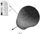
- FIG. 6 shows a three-dimensional gain diagram of the structure shown in FIG. 4 . It can be learned from FIG. 5 that a WiGig bandwidth with a return loss below -10 dB may be 54 GHz to 70 GHz. This represents that this design is a remarkable broadband design that has an extremely low signal loss.
- An embodiment of the present invention further provides an antenna, and the antenna includes a feed 30 and a power allocation network electrically connected to the feed 30.
- the power allocation network includes multiple patch antenna units 10 described in any one of the foregoing embodiments.
- the patch antenna unit 10 is fabricated by using a four-layer substrate 2.
- An antenna patch unit is disposed on a first-layer copper sheet and a second-layer copper sheet.
- a third layer is used as a ground plane, and a coupling slot 32 is disposed on the third layer, is used as a fourth layer to combine an integrated circuit and a pad, and is used for feed-in of a feeder.
- the coupling slot 32 on the third layer may be used to effectively feed high-frequency signals of a full-frequency band of 57-66 GHz into an antenna on the two higher layers for radiation.
- electromagnetic fields are generated at two ends of the feeder; a distributed current is induced by the two layers of radiation patches based on a magnetic field component in the electromagnetic fields and by means of the coupling slot; and an electromagnetic wave is generated based on the distributed current for radiation.
- a parasitic effect is reduced.
- a stacked structure increases an effective area of an antenna. A low parasitic parameter and a large effective area that are achieved provide the antenna with a high bandwidth and a high gain.
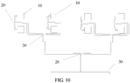
- FIG. 7 and FIG. 10 separately show different tree-like structures.
- FIG. 7 shows a structure in which two patch antenna units 10 are used.
- a feed 30 is connected to a power splitter 20, and each power splitter 20 is connected to a patch antenna unit 10.
- FIG. 8 and FIG. 9 show an emulation result of a return loss of the structure shown in FIG. 7
- FIG. 9 shows a three-dimensional gain diagram of the structure shown in FIG. 7 . It can be learned from data in FIG. 8 that a bandwidth with a return loss below -10 dB may be 54 GHz to 70 GHz.
- FIG. 10 shows a schematic diagram of a structure in which multiple patch antenna units 10 are used.
- lines are branched by using a power splitter 20, to form a tree-like structure.
- a feed 30 is connected to a power splitter 20; an output end of the power splitter 20 is separated into two branches, and each branch is connected to a power splitter 20; an output end of the power splitter 20 is further branched; and so on, until a last branch is connected to an antenna patch unit.
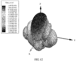
- FIG. 11 and FIG. 12 FIG.
- FIG. 11 shows an emulation result of a return loss of the structure shown in FIG. 10
- FIG. 12 shows a three-dimensional gain diagram of the structure shown in FIG. 10 . It can be learned that a bandwidth with a return loss below-10 dB may be 55 GHz to 70 GHz. This represents that this design is a remarkable broadband design that has an extremely low signal loss.
- an embodiment of the present invention further provides a communications device, and the communications device includes the foregoing antenna.
- a four-layer substrate 2 is used for fabrication.
- An antenna patch unit is disposed on a first-layer copper sheet and a second-layer copper sheet.
- a third layer is used as a ground plane, and a coupling slot 32 is disposed on the third layer, is used as a fourth layer to combine an integrated circuit and a pad, and is used for feed-in of a feeder.
- the coupling slot 32 on the third layer may be used to effectively feed high-frequency signals of a full-frequency band of 57-66 GHz into an antenna on the two higher layers for radiation.
- a parasitic effect is reduced.
- a stacked structure increases an effective area of an antenna. A low parasitic parameter and a large effective area that are achieved provides the antenna with a high bandwidth and a high gain.
Landscapes
- Physics & Mathematics (AREA)
- Electromagnetism (AREA)
- Engineering & Computer Science (AREA)
- Microelectronics & Electronic Packaging (AREA)
- Waveguide Aerials (AREA)
- Variable-Direction Aerials And Aerial Arrays (AREA)
Applications Claiming Priority (3)
| Application Number | Priority Date | Filing Date | Title |
|---|---|---|---|
| CN201610071196.2A CN105552550B (zh) | 2016-01-30 | 2016-01-30 | 一种贴片天线单元及天线 |
| PCT/CN2016/109322 WO2017128872A1 (fr) | 2016-01-30 | 2016-12-09 | Unité d'antenne à plaque et antenne |
| EP16887743.9A EP3401998B1 (fr) | 2016-01-30 | 2016-12-09 | Unité d'antenne à plaque et antenne |
Related Parent Applications (1)
| Application Number | Title | Priority Date | Filing Date |
|---|---|---|---|
| EP16887743.9A Division EP3401998B1 (fr) | 2016-01-30 | 2016-12-09 | Unité d'antenne à plaque et antenne |
Publications (2)
| Publication Number | Publication Date |
|---|---|
| EP3751663A1 true EP3751663A1 (fr) | 2020-12-16 |
| EP3751663B1 EP3751663B1 (fr) | 2023-05-31 |
Family
ID=55831595
Family Applications (2)
| Application Number | Title | Priority Date | Filing Date |
|---|---|---|---|
| EP16887743.9A Active EP3401998B1 (fr) | 2016-01-30 | 2016-12-09 | Unité d'antenne à plaque et antenne |
| EP20172863.1A Active EP3751663B1 (fr) | 2016-01-30 | 2016-12-09 | Unité d'antenne à plaque et antenne |
Family Applications Before (1)
| Application Number | Title | Priority Date | Filing Date |
|---|---|---|---|
| EP16887743.9A Active EP3401998B1 (fr) | 2016-01-30 | 2016-12-09 | Unité d'antenne à plaque et antenne |
Country Status (6)
| Country | Link |
|---|---|
| US (2) | US10727595B2 (fr) |
| EP (2) | EP3401998B1 (fr) |
| KR (1) | KR20180099897A (fr) |
| CN (3) | CN105552550B (fr) |
| TW (1) | TWI650901B (fr) |
| WO (1) | WO2017128872A1 (fr) |
Families Citing this family (61)
| Publication number | Priority date | Publication date | Assignee | Title |
|---|---|---|---|---|
| CN105552550B (zh) | 2016-01-30 | 2019-08-20 | 华为技术有限公司 | 一种贴片天线单元及天线 |
| US10201073B2 (en) * | 2016-05-31 | 2019-02-05 | Telefonaktiebolaget Lm Ericsson (Publ) | Multi-layer printed circuit board and a wireless communication node |
| CN106299627B (zh) * | 2016-10-18 | 2023-06-02 | 京东方科技集团股份有限公司 | 一种液晶天线及通信设备 |
| US10186779B2 (en) * | 2016-11-10 | 2019-01-22 | Advanced Semiconductor Engineering, Inc. | Semiconductor device package and method of manufacturing the same |
| WO2018119944A1 (fr) * | 2016-12-29 | 2018-07-05 | 深圳天珑无线科技有限公司 | Système d'antenne entrées multiples/sorties multiples et terminal mobile |
| US10396432B2 (en) * | 2017-01-23 | 2019-08-27 | Samsung Electro-Mechanics Co., Ltd. | Antenna-integrated radio frequency module |
| JP6855258B2 (ja) * | 2017-01-24 | 2021-04-07 | 原田工業株式会社 | 複合アンテナ装置 |
| US11205847B2 (en) * | 2017-02-01 | 2021-12-21 | Taoglas Group Holdings Limited | 5-6 GHz wideband dual-polarized massive MIMO antenna arrays |
| NO345389B1 (en) | 2017-03-15 | 2021-01-11 | Norbit Its | Patch antenna feed |
| CN107302130A (zh) * | 2017-05-11 | 2017-10-27 | 广东通宇通讯股份有限公司 | 天线阵列、天线模块及其微带天线单元 |
| JP6950084B2 (ja) * | 2017-05-15 | 2021-10-13 | ソニーグループ株式会社 | ミリ波通信用のパッチアンテナ |
| CN108879114A (zh) * | 2017-05-16 | 2018-11-23 | 华为技术有限公司 | 集成天线封装结构和终端 |
| CN108987910A (zh) * | 2017-06-02 | 2018-12-11 | 江苏万邦微电子有限公司 | 一种基于液晶电控扫描波导漏波天线 |
| KR102410799B1 (ko) | 2017-11-28 | 2022-06-21 | 삼성전자주식회사 | 밀리미터 웨이브 신호를 송/수신하기 위한 통신 장치 및 그 통신 장치를 포함하는 전자 장치 |
| US10833414B2 (en) * | 2018-03-02 | 2020-11-10 | Samsung Electro-Mechanics Co., Ltd. | Antenna apparatus and antenna module |
| CN108682949B (zh) * | 2018-06-11 | 2023-11-03 | 深圳迈睿智能科技有限公司 | 同一基板天线 |
| WO2020000250A1 (fr) * | 2018-06-27 | 2020-01-02 | 华为技术有限公司 | Structure de conditionnement d'antenne |
| CN109037908B (zh) * | 2018-07-05 | 2020-11-27 | 瑞声精密制造科技(常州)有限公司 | 移动终端的天线系统及移动终端 |
| US10854986B2 (en) * | 2018-07-18 | 2020-12-01 | Samsung Electro-Mechanics Co., Ltd. | Antenna apparatus |
| CN109216929A (zh) * | 2018-08-03 | 2019-01-15 | 西安电子科技大学 | 基于基片集成波导馈电的宽带缝隙耦合多层微带天线 |
| CN109149068B (zh) * | 2018-08-12 | 2021-04-02 | 瑞声科技(南京)有限公司 | 封装天线系统及移动终端 |
| CN111490333A (zh) * | 2018-11-06 | 2020-08-04 | 华为终端有限公司 | 耦合天线装置及电子设备 |
| CN109449573B (zh) * | 2018-11-14 | 2020-10-02 | 深圳Tcl新技术有限公司 | 微带天线和电视机 |
| KR102039398B1 (ko) | 2018-11-21 | 2019-11-01 | 연세대학교 산학협력단 | 복수의 주파수 대역에서 동작하는 통합 안테나 |
| CN209389213U (zh) * | 2018-12-31 | 2019-09-13 | 瑞声科技(新加坡)有限公司 | 滤波器天线 |
| US11469506B2 (en) * | 2019-01-17 | 2022-10-11 | Kyocera International, Inc. | Antenna apparatus with integrated filter |
| KR102111143B1 (ko) * | 2019-02-08 | 2020-05-14 | 국방과학연구소 | 반도체 온-칩 안테나 |
| US11742588B2 (en) * | 2019-02-13 | 2023-08-29 | Wisense Technologies Ltd. | System and method for feeding a patch antenna array |
| CN111697319B (zh) | 2019-03-12 | 2023-06-23 | 株式会社村田制作所 | 天线装置、天线模块以及通信装置 |
| CN111725607B (zh) * | 2019-03-20 | 2021-09-14 | Oppo广东移动通信有限公司 | 毫米波天线模组和电子设备 |
| KR102031203B1 (ko) * | 2019-03-20 | 2019-10-11 | 동우 화인켐 주식회사 | 안테나 적층체 및 이를 포함하는 화상 표시 장치 |
| CN111755805B (zh) * | 2019-03-28 | 2022-02-18 | Oppo广东移动通信有限公司 | 天线模组和电子设备 |
| CN111834731B (zh) | 2019-04-19 | 2022-03-01 | Oppo广东移动通信有限公司 | 天线模组及电子设备 |
| CN111864362A (zh) * | 2019-04-30 | 2020-10-30 | Oppo广东移动通信有限公司 | 天线模组及电子设备 |
| CN111864341B (zh) * | 2019-04-30 | 2022-05-06 | Oppo广东移动通信有限公司 | 天线组件及电子设备 |
| WO2020237559A1 (fr) | 2019-05-30 | 2020-12-03 | 华为技术有限公司 | Structure de conditionnement, dispositif réseau et dispositif terminal |
| US11177571B2 (en) * | 2019-08-07 | 2021-11-16 | Raytheon Company | Phased array antenna with edge-effect mitigation |
| CN112448136A (zh) * | 2019-08-27 | 2021-03-05 | 华为技术有限公司 | 天线及移动终端 |
| US11004801B2 (en) | 2019-08-28 | 2021-05-11 | Amkor Technology Singapore Holding Pte. Ltd. | Semiconductor devices and methods of manufacturing semiconductor devices |
| US11355451B2 (en) | 2019-08-28 | 2022-06-07 | Amkor Technology Singapore Holding Pte. Ltd. | Semiconductor devices and methods of manufacturing semiconductor devices |
| CN110474158A (zh) * | 2019-08-30 | 2019-11-19 | 维沃移动通信有限公司 | 一种天线单元及终端设备 |
| CN110620293B (zh) * | 2019-09-20 | 2021-06-11 | 上海无线电设备研究所 | 一种基于六臂螺旋阵列结构的稀疏阵天线 |
| CN111224217A (zh) * | 2020-01-08 | 2020-06-02 | Oppo广东移动通信有限公司 | 一种终端及通信方法 |
| JP7283623B2 (ja) * | 2020-02-19 | 2023-05-30 | 株式会社村田製作所 | アンテナモジュールおよびそれを搭載した通信装置 |
| CN113381167B (zh) | 2020-02-25 | 2022-11-01 | 荣耀终端有限公司 | 一种天线连接装置、天线组件和电子设备 |
| CN111430884B (zh) * | 2020-04-13 | 2021-07-20 | 维沃移动通信有限公司 | 一种天线模组及电子设备 |
| CN111613890B (zh) * | 2020-06-11 | 2023-07-14 | 维沃移动通信有限公司 | 天线结构及电子设备 |
| CN113871870B (zh) * | 2020-06-30 | 2023-02-10 | 华为技术有限公司 | 一种天线组件和电子设备 |
| CN111900543A (zh) * | 2020-08-12 | 2020-11-06 | 西安电子科技大学 | 基于耦合馈电的微带天线单元设计方法 |
| CN219513349U (zh) * | 2020-08-19 | 2023-08-11 | 株式会社村田制作所 | 通信装置 |
| CN114843749B (zh) * | 2021-02-01 | 2025-06-17 | 深圳引望智能技术有限公司 | 天线、探测装置、雷达及终端 |
| IT202100003860A1 (it) * | 2021-02-19 | 2022-08-19 | Ask Ind Spa | Antenna ad onde millimetriche per applicazioni 5g e veicolo comprendente tale antenna |
| TWI773417B (zh) * | 2021-07-02 | 2022-08-01 | 特崴光波導股份有限公司 | 耦合式陣列天線及其裝置 |
| CN116111335B (zh) * | 2021-11-10 | 2025-08-26 | 财团法人工业技术研究院 | 透光天线 |
| EP4352822A4 (fr) | 2021-12-02 | 2024-10-23 | Samsung Electronics Co., Ltd. | Antenne intégrée de carte de circuit imprimé pour émettre/recevoir des données |
| CN114400441B (zh) | 2022-03-24 | 2022-09-02 | 荣耀终端有限公司 | 天线、超宽带天线阵列及电子设备 |
| TWI845937B (zh) * | 2022-05-07 | 2024-06-21 | 富智康國際股份有限公司 | 天線饋入耦合模組及電子裝置 |
| FR3137798B1 (fr) * | 2022-07-07 | 2024-07-19 | Thales Sa | Antenne élémentaire améliorée du type plan rayonnant alimenté par fentes et antenne réseau active |
| CN115566008B (zh) * | 2022-09-29 | 2026-04-28 | 中国电子科技集团公司第三十八研究所 | 带状线过渡的毫米波芯片封装结构 |
| US12476375B2 (en) | 2022-10-14 | 2025-11-18 | Samsung Electronics Co., Ltd. | MM-wave resonant termination load embedded in a PCB substrate and antenna array including the same |
| CN116914415A (zh) * | 2023-07-17 | 2023-10-20 | 濠玮电子科技(惠州)有限公司 | 一种网点印刷导电银浆油墨的缝隙耦合贴片天线 |
Citations (1)
| Publication number | Priority date | Publication date | Assignee | Title |
|---|---|---|---|---|
| US6181278B1 (en) * | 1997-03-21 | 2001-01-30 | Sharp Kabushiki Kaisha | Antenna-integral high frequency circuit electromagnetically coupling feeder circuit connected to high frequency circuit to microstrip antenna via slot coupling hole |
Family Cites Families (25)
| Publication number | Priority date | Publication date | Assignee | Title |
|---|---|---|---|---|
| US4847625A (en) * | 1988-02-16 | 1989-07-11 | Ford Aerospace Corporation | Wideband, aperture-coupled microstrip antenna |
| US5043738A (en) * | 1990-03-15 | 1991-08-27 | Hughes Aircraft Company | Plural frequency patch antenna assembly |
| US5241321A (en) * | 1992-05-15 | 1993-08-31 | Space Systems/Loral, Inc. | Dual frequency circularly polarized microwave antenna |
| US5461393A (en) * | 1993-08-20 | 1995-10-24 | Texas Instruments Incorporated | Dual frequency cavity backed slot antenna |
| SE517218C2 (sv) * | 1999-09-03 | 2002-05-07 | Ericsson Telefon Ab L M | En lågprofilantennstruktur samt en anordning innefattande trådlöst kommunikationsmedel, en trådlös mobil terminal, ett datorkort lämpligt för införande i en elektronisk anordning och ett lokalt nätverkssystem innefattande en basstation och ett flertal terminaler vilka är i trådlös kommunikation med basstationen innefattande en sådan lågprofilantennstruktur |
| FR2822301B1 (fr) * | 2001-03-15 | 2004-06-04 | Cit Alcatel | Antenne a bande elargie pour appareils mobiles |
| JP2004527180A (ja) * | 2001-04-30 | 2004-09-02 | ミッション・テレコム・インコーポレーテッド | 広帯域デュアル偏波マイクロストリップアレイアンテナ |
| TWI280687B (en) * | 2002-08-09 | 2007-05-01 | Wistron Neweb Corp | Multi-patch antenna which can transmit radio signals with two frequencies |
| US6856300B2 (en) * | 2002-11-08 | 2005-02-15 | Kvh Industries, Inc. | Feed network and method for an offset stacked patch antenna array |
| US6995711B2 (en) * | 2003-03-31 | 2006-02-07 | Harris Corporation | High efficiency crossed slot microstrip antenna |
| JP4684730B2 (ja) * | 2004-04-30 | 2011-05-18 | シャープ株式会社 | 高周波半導体装置、送信装置および受信装置 |
| CN101064381A (zh) * | 2006-04-24 | 2007-10-31 | 中国科学院空间科学与应用研究中心 | 一种用于无线电掩星探测的双频gps天线 |
| US9172145B2 (en) * | 2006-09-21 | 2015-10-27 | Raytheon Company | Transmit/receive daughter card with integral circulator |
| CN101141023B (zh) * | 2007-09-07 | 2011-12-07 | 中国电子科技集团公司第五十五研究所 | 微机电层叠式毫米波天线 |
| US7692590B2 (en) * | 2008-02-20 | 2010-04-06 | International Business Machines Corporation | Radio frequency (RF) integrated circuit (IC) packages with integrated aperture-coupled patch antenna(s) |
| US7696930B2 (en) * | 2008-04-14 | 2010-04-13 | International Business Machines Corporation | Radio frequency (RF) integrated circuit (IC) packages with integrated aperture-coupled patch antenna(s) in ring and/or offset cavities |
| US8256685B2 (en) * | 2009-06-30 | 2012-09-04 | International Business Machines Corporation | Compact millimeter wave packages with integrated antennas |
| US8482475B2 (en) * | 2009-07-31 | 2013-07-09 | Viasat, Inc. | Method and apparatus for a compact modular phased array element |
| US9142889B2 (en) | 2010-02-02 | 2015-09-22 | Technion Research & Development Foundation Ltd. | Compact tapered slot antenna |
| CN102195143A (zh) | 2011-03-10 | 2011-09-21 | 东南大学 | 带倾角的宽带并馈全向天线阵 |
| CN102299418B (zh) * | 2011-06-15 | 2013-09-18 | 集美大学 | 多层宽频微带天线 |
| KR101255947B1 (ko) * | 2011-10-05 | 2013-04-23 | 삼성전기주식회사 | 대역폭 조절 가능한 유전체 공진기 안테나 |
| CN103066385B (zh) * | 2012-12-22 | 2015-08-05 | 西安电子科技大学 | 用于系统级封装的ltcc双层微带天线 |
| CN104157982A (zh) * | 2014-07-07 | 2014-11-19 | 华东交通大学 | 一种基于ebg结构的双极化mimo天线 |
| CN105552550B (zh) * | 2016-01-30 | 2019-08-20 | 华为技术有限公司 | 一种贴片天线单元及天线 |
-
2016
- 2016-01-30 CN CN201610071196.2A patent/CN105552550B/zh active Active
- 2016-01-30 CN CN201910749630.1A patent/CN110611160B/zh active Active
- 2016-01-30 CN CN201910750419.1A patent/CN110600872B/zh active Active
- 2016-12-09 WO PCT/CN2016/109322 patent/WO2017128872A1/fr not_active Ceased
- 2016-12-09 EP EP16887743.9A patent/EP3401998B1/fr active Active
- 2016-12-09 KR KR1020187024036A patent/KR20180099897A/ko not_active Withdrawn
- 2016-12-09 EP EP20172863.1A patent/EP3751663B1/fr active Active
-
2017
- 2017-01-25 TW TW106102933A patent/TWI650901B/zh active
-
2018
- 2018-07-30 US US16/049,104 patent/US10727595B2/en active Active
-
2020
- 2020-05-12 US US16/872,920 patent/US11189927B2/en active Active
Patent Citations (1)
| Publication number | Priority date | Publication date | Assignee | Title |
|---|---|---|---|---|
| US6181278B1 (en) * | 1997-03-21 | 2001-01-30 | Sharp Kabushiki Kaisha | Antenna-integral high frequency circuit electromagnetically coupling feeder circuit connected to high frequency circuit to microstrip antenna via slot coupling hole |
Non-Patent Citations (3)
| Title |
|---|
| JOHAN GRANHOLM ET AL: "Dual Polarization Stacked Microstrip Patch Antenna Array With Very Low Cross-Polarization", IEEE TRANSACTIONS ON ANTENNAS AND PROPAGATION, IEEE SERVICE CENTER, PISCATAWAY, NJ, US, vol. 49, no. 10, 1 October 2001 (2001-10-01), XP011004126, ISSN: 0018-926X * |
| UEDA HIDEKI ET AL: "Small and low profile stacked patch antenna with wide bandwidth and stable radiation pattern", 2013 IEEE ANTENNAS AND PROPAGATION SOCIETY INTERNATIONAL SYMPOSIUM (APSURSI), IEEE, 6 July 2014 (2014-07-06), pages 1875 - 1876, XP032645552, ISSN: 1522-3965, ISBN: 978-1-4799-3538-3, [retrieved on 20140918], DOI: 10.1109/APS.2014.6905264 * |
| WONBIN HONG ET AL: "Grid Assembly-Free 60-GHz Antenna Module Embedded in FR-4 Transceiver Carrier Board", IEEE TRANSACTIONS ON ANTENNAS AND PROPAGATION, IEEE SERVICE CENTER, PISCATAWAY, NJ, US, vol. 61, no. 4, 1 April 2013 (2013-04-01), pages 1573 - 1580, XP011499222, ISSN: 0018-926X, DOI: 10.1109/TAP.2012.2232635 * |
Also Published As
| Publication number | Publication date |
|---|---|
| US10727595B2 (en) | 2020-07-28 |
| TW201728002A (zh) | 2017-08-01 |
| CN110600872B (zh) | 2023-09-12 |
| CN110600872A (zh) | 2019-12-20 |
| US20180337456A1 (en) | 2018-11-22 |
| WO2017128872A1 (fr) | 2017-08-03 |
| EP3751663B1 (fr) | 2023-05-31 |
| US11189927B2 (en) | 2021-11-30 |
| US20200280132A1 (en) | 2020-09-03 |
| TWI650901B (zh) | 2019-02-11 |
| CN105552550B (zh) | 2019-08-20 |
| KR20180099897A (ko) | 2018-09-05 |
| CN105552550A (zh) | 2016-05-04 |
| CN110611160A (zh) | 2019-12-24 |
| EP3401998B1 (fr) | 2020-05-13 |
| CN110611160B (zh) | 2021-08-03 |
| EP3401998A4 (fr) | 2019-01-16 |
| EP3401998A1 (fr) | 2018-11-14 |
Similar Documents
| Publication | Publication Date | Title |
|---|---|---|
| US11189927B2 (en) | Patch antenna unit and antenna | |
| CN109845034B (zh) | 天线元件、天线模块以及通信装置 | |
| US11223120B2 (en) | Antenna module and antenna device | |
| CN105493348B (zh) | 多波段共口径天线 | |
| CN109149068B (zh) | 封装天线系统及移动终端 | |
| US10103449B2 (en) | Antenna array | |
| US9819098B2 (en) | Antenna-in-package structures with broadside and end-fire radiations | |
| US10263336B1 (en) | Multi-band multi-antenna array | |
| US20180123245A1 (en) | Broadband antenna array for wireless communications | |
| WO2020034715A1 (fr) | Système d'antenne aog et terminal mobile | |
| US20100033393A1 (en) | Techniques for Mounting a Millimeter Wave Antenna and a Radio Frequency Integrated Circuit Onto a PCB | |
| US11322819B2 (en) | Antenna module | |
| US8330552B2 (en) | Sandwich structure for directional coupler | |
| US12095163B2 (en) | Antenna module and communication device equipped with the same | |
| US10461439B2 (en) | Flexible polymer antenna with multiple ground resonators | |
| US12218432B2 (en) | Antenna module and communication apparatus equipped with the same | |
| US12206169B2 (en) | Antenna module | |
| CN111656608A (zh) | 多频段天线、无线通信组件和无线通信装置 | |
| US11929557B2 (en) | Antenna module and communication device equipped with the same | |
| US20120326940A1 (en) | Multi-band antenna and electronic apparatus having the same | |
| US20200411946A1 (en) | Antenna device and on-board equipment | |
| CN105742804A (zh) | 同轴馈电电容加载的三极化槽缝天线 |
Legal Events
| Date | Code | Title | Description |
|---|---|---|---|
| PUAI | Public reference made under article 153(3) epc to a published international application that has entered the european phase |
Free format text: ORIGINAL CODE: 0009012 |
|
| STAA | Information on the status of an ep patent application or granted ep patent |
Free format text: STATUS: THE APPLICATION HAS BEEN PUBLISHED |
|
| AC | Divisional application: reference to earlier application |
Ref document number: 3401998 Country of ref document: EP Kind code of ref document: P |
|
| AK | Designated contracting states |
Kind code of ref document: A1 Designated state(s): AL AT BE BG CH CY CZ DE DK EE ES FI FR GB GR HR HU IE IS IT LI LT LU LV MC MK MT NL NO PL PT RO RS SE SI SK SM TR |
|
| STAA | Information on the status of an ep patent application or granted ep patent |
Free format text: STATUS: REQUEST FOR EXAMINATION WAS MADE |
|
| 17P | Request for examination filed |
Effective date: 20210603 |
|
| RBV | Designated contracting states (corrected) |
Designated state(s): AL AT BE BG CH CY CZ DE DK EE ES FI FR GB GR HR HU IE IS IT LI LT LU LV MC MK MT NL NO PL PT RO RS SE SI SK SM TR |
|
| REG | Reference to a national code |
Ref country code: DE Ref legal event code: R079 Free format text: PREVIOUS MAIN CLASS: H01Q0001380000 Ipc: H01Q0009040000 Ref country code: DE Ref legal event code: R079 Ref document number: 602016079769 Country of ref document: DE Free format text: PREVIOUS MAIN CLASS: H01Q0001380000 Ipc: H01Q0009040000 |
|
| GRAP | Despatch of communication of intention to grant a patent |
Free format text: ORIGINAL CODE: EPIDOSNIGR1 |
|
| STAA | Information on the status of an ep patent application or granted ep patent |
Free format text: STATUS: GRANT OF PATENT IS INTENDED |
|
| RIC1 | Information provided on ipc code assigned before grant |
Ipc: H01Q 21/08 20060101ALI20221219BHEP Ipc: H01Q 21/06 20060101ALI20221219BHEP Ipc: H01Q 21/00 20060101ALI20221219BHEP Ipc: H01Q 1/22 20060101ALI20221219BHEP Ipc: H01Q 9/04 20060101AFI20221219BHEP |
|
| INTG | Intention to grant announced |
Effective date: 20230125 |
|
| GRAS | Grant fee paid |
Free format text: ORIGINAL CODE: EPIDOSNIGR3 |
|
| GRAA | (expected) grant |
Free format text: ORIGINAL CODE: 0009210 |
|
| STAA | Information on the status of an ep patent application or granted ep patent |
Free format text: STATUS: THE PATENT HAS BEEN GRANTED |
|
| AC | Divisional application: reference to earlier application |
Ref document number: 3401998 Country of ref document: EP Kind code of ref document: P |
|
| AK | Designated contracting states |
Kind code of ref document: B1 Designated state(s): AL AT BE BG CH CY CZ DE DK EE ES FI FR GB GR HR HU IE IS IT LI LT LU LV MC MK MT NL NO PL PT RO RS SE SI SK SM TR |
|
| REG | Reference to a national code |
Ref country code: GB Ref legal event code: FG4D Ref country code: CH Ref legal event code: EP |
|
| REG | Reference to a national code |
Ref country code: AT Ref legal event code: REF Ref document number: 1571526 Country of ref document: AT Kind code of ref document: T Effective date: 20230615 Ref country code: DE Ref legal event code: R096 Ref document number: 602016079769 Country of ref document: DE |
|
| REG | Reference to a national code |
Ref country code: IE Ref legal event code: FG4D |
|
| REG | Reference to a national code |
Ref country code: LT Ref legal event code: MG9D |
|
| REG | Reference to a national code |
Ref country code: NL Ref legal event code: MP Effective date: 20230531 |
|
| REG | Reference to a national code |
Ref country code: AT Ref legal event code: MK05 Ref document number: 1571526 Country of ref document: AT Kind code of ref document: T Effective date: 20230531 |
|
| PG25 | Lapsed in a contracting state [announced via postgrant information from national office to epo] |
Ref country code: SE Free format text: LAPSE BECAUSE OF FAILURE TO SUBMIT A TRANSLATION OF THE DESCRIPTION OR TO PAY THE FEE WITHIN THE PRESCRIBED TIME-LIMIT Effective date: 20230531 Ref country code: NO Free format text: LAPSE BECAUSE OF FAILURE TO SUBMIT A TRANSLATION OF THE DESCRIPTION OR TO PAY THE FEE WITHIN THE PRESCRIBED TIME-LIMIT Effective date: 20230831 Ref country code: ES Free format text: LAPSE BECAUSE OF FAILURE TO SUBMIT A TRANSLATION OF THE DESCRIPTION OR TO PAY THE FEE WITHIN THE PRESCRIBED TIME-LIMIT Effective date: 20230531 Ref country code: AT Free format text: LAPSE BECAUSE OF FAILURE TO SUBMIT A TRANSLATION OF THE DESCRIPTION OR TO PAY THE FEE WITHIN THE PRESCRIBED TIME-LIMIT Effective date: 20230531 |
|
| PG25 | Lapsed in a contracting state [announced via postgrant information from national office to epo] |
Ref country code: RS Free format text: LAPSE BECAUSE OF FAILURE TO SUBMIT A TRANSLATION OF THE DESCRIPTION OR TO PAY THE FEE WITHIN THE PRESCRIBED TIME-LIMIT Effective date: 20230531 Ref country code: PL Free format text: LAPSE BECAUSE OF FAILURE TO SUBMIT A TRANSLATION OF THE DESCRIPTION OR TO PAY THE FEE WITHIN THE PRESCRIBED TIME-LIMIT Effective date: 20230531 Ref country code: NL Free format text: LAPSE BECAUSE OF FAILURE TO SUBMIT A TRANSLATION OF THE DESCRIPTION OR TO PAY THE FEE WITHIN THE PRESCRIBED TIME-LIMIT Effective date: 20230531 Ref country code: LV Free format text: LAPSE BECAUSE OF FAILURE TO SUBMIT A TRANSLATION OF THE DESCRIPTION OR TO PAY THE FEE WITHIN THE PRESCRIBED TIME-LIMIT Effective date: 20230531 Ref country code: LT Free format text: LAPSE BECAUSE OF FAILURE TO SUBMIT A TRANSLATION OF THE DESCRIPTION OR TO PAY THE FEE WITHIN THE PRESCRIBED TIME-LIMIT Effective date: 20230531 Ref country code: IS Free format text: LAPSE BECAUSE OF FAILURE TO SUBMIT A TRANSLATION OF THE DESCRIPTION OR TO PAY THE FEE WITHIN THE PRESCRIBED TIME-LIMIT Effective date: 20230930 Ref country code: HR Free format text: LAPSE BECAUSE OF FAILURE TO SUBMIT A TRANSLATION OF THE DESCRIPTION OR TO PAY THE FEE WITHIN THE PRESCRIBED TIME-LIMIT Effective date: 20230531 Ref country code: GR Free format text: LAPSE BECAUSE OF FAILURE TO SUBMIT A TRANSLATION OF THE DESCRIPTION OR TO PAY THE FEE WITHIN THE PRESCRIBED TIME-LIMIT Effective date: 20230901 |
|
| PG25 | Lapsed in a contracting state [announced via postgrant information from national office to epo] |
Ref country code: FI Free format text: LAPSE BECAUSE OF FAILURE TO SUBMIT A TRANSLATION OF THE DESCRIPTION OR TO PAY THE FEE WITHIN THE PRESCRIBED TIME-LIMIT Effective date: 20230531 |
|
| PG25 | Lapsed in a contracting state [announced via postgrant information from national office to epo] |
Ref country code: SK Free format text: LAPSE BECAUSE OF FAILURE TO SUBMIT A TRANSLATION OF THE DESCRIPTION OR TO PAY THE FEE WITHIN THE PRESCRIBED TIME-LIMIT Effective date: 20230531 |
|
| PG25 | Lapsed in a contracting state [announced via postgrant information from national office to epo] |
Ref country code: SM Free format text: LAPSE BECAUSE OF FAILURE TO SUBMIT A TRANSLATION OF THE DESCRIPTION OR TO PAY THE FEE WITHIN THE PRESCRIBED TIME-LIMIT Effective date: 20230531 Ref country code: SK Free format text: LAPSE BECAUSE OF FAILURE TO SUBMIT A TRANSLATION OF THE DESCRIPTION OR TO PAY THE FEE WITHIN THE PRESCRIBED TIME-LIMIT Effective date: 20230531 Ref country code: RO Free format text: LAPSE BECAUSE OF FAILURE TO SUBMIT A TRANSLATION OF THE DESCRIPTION OR TO PAY THE FEE WITHIN THE PRESCRIBED TIME-LIMIT Effective date: 20230531 Ref country code: PT Free format text: LAPSE BECAUSE OF FAILURE TO SUBMIT A TRANSLATION OF THE DESCRIPTION OR TO PAY THE FEE WITHIN THE PRESCRIBED TIME-LIMIT Effective date: 20231002 Ref country code: EE Free format text: LAPSE BECAUSE OF FAILURE TO SUBMIT A TRANSLATION OF THE DESCRIPTION OR TO PAY THE FEE WITHIN THE PRESCRIBED TIME-LIMIT Effective date: 20230531 Ref country code: DK Free format text: LAPSE BECAUSE OF FAILURE TO SUBMIT A TRANSLATION OF THE DESCRIPTION OR TO PAY THE FEE WITHIN THE PRESCRIBED TIME-LIMIT Effective date: 20230531 Ref country code: CZ Free format text: LAPSE BECAUSE OF FAILURE TO SUBMIT A TRANSLATION OF THE DESCRIPTION OR TO PAY THE FEE WITHIN THE PRESCRIBED TIME-LIMIT Effective date: 20230531 |
|
| REG | Reference to a national code |
Ref country code: DE Ref legal event code: R097 Ref document number: 602016079769 Country of ref document: DE |
|
| PLBE | No opposition filed within time limit |
Free format text: ORIGINAL CODE: 0009261 |
|
| STAA | Information on the status of an ep patent application or granted ep patent |
Free format text: STATUS: NO OPPOSITION FILED WITHIN TIME LIMIT |
|
| PG25 | Lapsed in a contracting state [announced via postgrant information from national office to epo] |
Ref country code: SI Free format text: LAPSE BECAUSE OF FAILURE TO SUBMIT A TRANSLATION OF THE DESCRIPTION OR TO PAY THE FEE WITHIN THE PRESCRIBED TIME-LIMIT Effective date: 20230531 |
|
| 26N | No opposition filed |
Effective date: 20240301 |
|
| PG25 | Lapsed in a contracting state [announced via postgrant information from national office to epo] |
Ref country code: SI Free format text: LAPSE BECAUSE OF FAILURE TO SUBMIT A TRANSLATION OF THE DESCRIPTION OR TO PAY THE FEE WITHIN THE PRESCRIBED TIME-LIMIT Effective date: 20230531 Ref country code: IT Free format text: LAPSE BECAUSE OF FAILURE TO SUBMIT A TRANSLATION OF THE DESCRIPTION OR TO PAY THE FEE WITHIN THE PRESCRIBED TIME-LIMIT Effective date: 20230531 |
|
| REG | Reference to a national code |
Ref country code: CH Ref legal event code: PL |
|
| PG25 | Lapsed in a contracting state [announced via postgrant information from national office to epo] |
Ref country code: LU Free format text: LAPSE BECAUSE OF NON-PAYMENT OF DUE FEES Effective date: 20231209 |
|
| PG25 | Lapsed in a contracting state [announced via postgrant information from national office to epo] |
Ref country code: MC Free format text: LAPSE BECAUSE OF FAILURE TO SUBMIT A TRANSLATION OF THE DESCRIPTION OR TO PAY THE FEE WITHIN THE PRESCRIBED TIME-LIMIT Effective date: 20230531 |
|
| REG | Reference to a national code |
Ref country code: BE Ref legal event code: MM Effective date: 20231231 |
|
| PG25 | Lapsed in a contracting state [announced via postgrant information from national office to epo] |
Ref country code: MC Free format text: LAPSE BECAUSE OF FAILURE TO SUBMIT A TRANSLATION OF THE DESCRIPTION OR TO PAY THE FEE WITHIN THE PRESCRIBED TIME-LIMIT Effective date: 20230531 Ref country code: LU Free format text: LAPSE BECAUSE OF NON-PAYMENT OF DUE FEES Effective date: 20231209 |
|
| REG | Reference to a national code |
Ref country code: IE Ref legal event code: MM4A |
|
| PG25 | Lapsed in a contracting state [announced via postgrant information from national office to epo] |
Ref country code: IE Free format text: LAPSE BECAUSE OF NON-PAYMENT OF DUE FEES Effective date: 20231209 |
|
| PG25 | Lapsed in a contracting state [announced via postgrant information from national office to epo] |
Ref country code: BE Free format text: LAPSE BECAUSE OF NON-PAYMENT OF DUE FEES Effective date: 20231231 |
|
| PG25 | Lapsed in a contracting state [announced via postgrant information from national office to epo] |
Ref country code: CH Free format text: LAPSE BECAUSE OF NON-PAYMENT OF DUE FEES Effective date: 20231231 |
|
| PG25 | Lapsed in a contracting state [announced via postgrant information from national office to epo] |
Ref country code: IE Free format text: LAPSE BECAUSE OF NON-PAYMENT OF DUE FEES Effective date: 20231209 Ref country code: CH Free format text: LAPSE BECAUSE OF NON-PAYMENT OF DUE FEES Effective date: 20231231 Ref country code: BE Free format text: LAPSE BECAUSE OF NON-PAYMENT OF DUE FEES Effective date: 20231231 |
|
| PG25 | Lapsed in a contracting state [announced via postgrant information from national office to epo] |
Ref country code: BG Free format text: LAPSE BECAUSE OF FAILURE TO SUBMIT A TRANSLATION OF THE DESCRIPTION OR TO PAY THE FEE WITHIN THE PRESCRIBED TIME-LIMIT Effective date: 20230531 |
|
| PG25 | Lapsed in a contracting state [announced via postgrant information from national office to epo] |
Ref country code: BG Free format text: LAPSE BECAUSE OF FAILURE TO SUBMIT A TRANSLATION OF THE DESCRIPTION OR TO PAY THE FEE WITHIN THE PRESCRIBED TIME-LIMIT Effective date: 20230531 |
|
| PG25 | Lapsed in a contracting state [announced via postgrant information from national office to epo] |
Ref country code: CY Free format text: LAPSE BECAUSE OF FAILURE TO SUBMIT A TRANSLATION OF THE DESCRIPTION OR TO PAY THE FEE WITHIN THE PRESCRIBED TIME-LIMIT; INVALID AB INITIO Effective date: 20161209 |
|
| PG25 | Lapsed in a contracting state [announced via postgrant information from national office to epo] |
Ref country code: HU Free format text: LAPSE BECAUSE OF FAILURE TO SUBMIT A TRANSLATION OF THE DESCRIPTION OR TO PAY THE FEE WITHIN THE PRESCRIBED TIME-LIMIT; INVALID AB INITIO Effective date: 20161209 |
|
| PG25 | Lapsed in a contracting state [announced via postgrant information from national office to epo] |
Ref country code: TR Free format text: LAPSE BECAUSE OF FAILURE TO SUBMIT A TRANSLATION OF THE DESCRIPTION OR TO PAY THE FEE WITHIN THE PRESCRIBED TIME-LIMIT Effective date: 20230531 |
|
| PGFP | Annual fee paid to national office [announced via postgrant information from national office to epo] |
Ref country code: DE Payment date: 20251104 Year of fee payment: 10 |
|
| PGFP | Annual fee paid to national office [announced via postgrant information from national office to epo] |
Ref country code: GB Payment date: 20251030 Year of fee payment: 10 |
|
| PGFP | Annual fee paid to national office [announced via postgrant information from national office to epo] |
Ref country code: FR Payment date: 20251110 Year of fee payment: 10 |