EP3749066A1 - Glass core device, and method for manufacturing same - Google Patents
Glass core device, and method for manufacturing same Download PDFInfo
- Publication number
- EP3749066A1 EP3749066A1 EP19747585.8A EP19747585A EP3749066A1 EP 3749066 A1 EP3749066 A1 EP 3749066A1 EP 19747585 A EP19747585 A EP 19747585A EP 3749066 A1 EP3749066 A1 EP 3749066A1
- Authority
- EP
- European Patent Office
- Prior art keywords
- glass core
- glass
- wiring pattern
- core
- vias
- Prior art date
- Legal status (The legal status is an assumption and is not a legal conclusion. Google has not performed a legal analysis and makes no representation as to the accuracy of the status listed.)
- Granted
Links
Images




Classifications
-
- H—ELECTRICITY
- H10—SEMICONDUCTOR DEVICES; ELECTRIC SOLID-STATE DEVICES NOT OTHERWISE PROVIDED FOR
- H10W—GENERIC PACKAGES, INTERCONNECTIONS, CONNECTORS OR OTHER CONSTRUCTIONAL DETAILS OF DEVICES COVERED BY CLASS H10
- H10W70/00—Package substrates; Interposers; Redistribution layers [RDL]
- H10W70/60—Insulating or insulated package substrates; Interposers; Redistribution layers
- H10W70/62—Insulating or insulated package substrates; Interposers; Redistribution layers characterised by their interconnections
- H10W70/63—Vias, e.g. via plugs
- H10W70/635—Through-vias
-
- H—ELECTRICITY
- H05—ELECTRIC TECHNIQUES NOT OTHERWISE PROVIDED FOR
- H05K—PRINTED CIRCUITS; CASINGS OR CONSTRUCTIONAL DETAILS OF ELECTRIC APPARATUS; MANUFACTURE OF ASSEMBLAGES OF ELECTRICAL COMPONENTS
- H05K3/00—Apparatus or processes for manufacturing printed circuits
- H05K3/0011—Working of insulating substrates or insulating layers
- H05K3/0017—Etching of the substrate by chemical or physical means
-
- H—ELECTRICITY
- H01—ELECTRIC ELEMENTS
- H01F—MAGNETS; INDUCTANCES; TRANSFORMERS; SELECTION OF MATERIALS FOR THEIR MAGNETIC PROPERTIES
- H01F17/00—Fixed inductances of the signal type
- H01F17/0006—Printed inductances
- H01F17/0013—Printed inductances with stacked layers
-
- H—ELECTRICITY
- H01—ELECTRIC ELEMENTS
- H01F—MAGNETS; INDUCTANCES; TRANSFORMERS; SELECTION OF MATERIALS FOR THEIR MAGNETIC PROPERTIES
- H01F41/00—Apparatus or processes specially adapted for manufacturing or assembling magnets, inductances or transformers; Apparatus or processes specially adapted for manufacturing materials characterised by their magnetic properties
- H01F41/02—Apparatus or processes specially adapted for manufacturing or assembling magnets, inductances or transformers; Apparatus or processes specially adapted for manufacturing materials characterised by their magnetic properties for manufacturing cores, coils, or magnets
- H01F41/04—Apparatus or processes specially adapted for manufacturing or assembling magnets, inductances or transformers; Apparatus or processes specially adapted for manufacturing materials characterised by their magnetic properties for manufacturing cores, coils, or magnets for manufacturing coils
- H01F41/041—Printed circuit coils
- H01F41/042—Printed circuit coils by thin film techniques
-
- H—ELECTRICITY
- H05—ELECTRIC TECHNIQUES NOT OTHERWISE PROVIDED FOR
- H05K—PRINTED CIRCUITS; CASINGS OR CONSTRUCTIONAL DETAILS OF ELECTRIC APPARATUS; MANUFACTURE OF ASSEMBLAGES OF ELECTRICAL COMPONENTS
- H05K3/00—Apparatus or processes for manufacturing printed circuits
- H05K3/0011—Working of insulating substrates or insulating layers
- H05K3/0044—Mechanical working of the substrate, e.g. drilling or punching
- H05K3/0052—Depaneling, i.e. dividing a panel into circuit boards; Working of the edges of circuit boards
-
- H—ELECTRICITY
- H05—ELECTRIC TECHNIQUES NOT OTHERWISE PROVIDED FOR
- H05K—PRINTED CIRCUITS; CASINGS OR CONSTRUCTIONAL DETAILS OF ELECTRIC APPARATUS; MANUFACTURE OF ASSEMBLAGES OF ELECTRICAL COMPONENTS
- H05K3/00—Apparatus or processes for manufacturing printed circuits
- H05K3/22—Secondary treatment of printed circuits
- H05K3/28—Applying non-metallic protective coatings
-
- H—ELECTRICITY
- H05—ELECTRIC TECHNIQUES NOT OTHERWISE PROVIDED FOR
- H05K—PRINTED CIRCUITS; CASINGS OR CONSTRUCTIONAL DETAILS OF ELECTRIC APPARATUS; MANUFACTURE OF ASSEMBLAGES OF ELECTRICAL COMPONENTS
- H05K3/00—Apparatus or processes for manufacturing printed circuits
- H05K3/40—Forming printed elements for providing electric connections to or between printed circuits
- H05K3/42—Plated through-holes or plated via connections
- H05K3/425—Plated through-holes or plated via connections characterised by the sequence of steps for plating the through-holes or via connections in relation to the conductive pattern
- H05K3/426—Plated through-holes or plated via connections characterised by the sequence of steps for plating the through-holes or via connections in relation to the conductive pattern initial plating of through-holes in substrates without metal
-
- H—ELECTRICITY
- H10—SEMICONDUCTOR DEVICES; ELECTRIC SOLID-STATE DEVICES NOT OTHERWISE PROVIDED FOR
- H10W—GENERIC PACKAGES, INTERCONNECTIONS, CONNECTORS OR OTHER CONSTRUCTIONAL DETAILS OF DEVICES COVERED BY CLASS H10
- H10W20/00—Interconnections in chips, wafers or substrates
- H10W20/01—Manufacture or treatment
- H10W20/071—Manufacture or treatment of dielectric parts thereof
- H10W20/081—Manufacture or treatment of dielectric parts thereof by forming openings in the dielectric parts
-
- H—ELECTRICITY
- H10—SEMICONDUCTOR DEVICES; ELECTRIC SOLID-STATE DEVICES NOT OTHERWISE PROVIDED FOR
- H10W—GENERIC PACKAGES, INTERCONNECTIONS, CONNECTORS OR OTHER CONSTRUCTIONAL DETAILS OF DEVICES COVERED BY CLASS H10
- H10W70/00—Package substrates; Interposers; Redistribution layers [RDL]
- H10W70/01—Manufacture or treatment
- H10W70/05—Manufacture or treatment of insulating or insulated package substrates, or of interposers, or of redistribution layers
- H10W70/095—Manufacture or treatment of insulating or insulated package substrates, or of interposers, or of redistribution layers of vias therein
-
- H—ELECTRICITY
- H10—SEMICONDUCTOR DEVICES; ELECTRIC SOLID-STATE DEVICES NOT OTHERWISE PROVIDED FOR
- H10W—GENERIC PACKAGES, INTERCONNECTIONS, CONNECTORS OR OTHER CONSTRUCTIONAL DETAILS OF DEVICES COVERED BY CLASS H10
- H10W70/00—Package substrates; Interposers; Redistribution layers [RDL]
- H10W70/60—Insulating or insulated package substrates; Interposers; Redistribution layers
- H10W70/67—Insulating or insulated package substrates; Interposers; Redistribution layers characterised by their insulating layers or insulating parts
- H10W70/69—Insulating materials thereof
- H10W70/692—Ceramics or glasses
-
- H—ELECTRICITY
- H05—ELECTRIC TECHNIQUES NOT OTHERWISE PROVIDED FOR
- H05K—PRINTED CIRCUITS; CASINGS OR CONSTRUCTIONAL DETAILS OF ELECTRIC APPARATUS; MANUFACTURE OF ASSEMBLAGES OF ELECTRICAL COMPONENTS
- H05K1/00—Printed circuits
- H05K1/16—Printed circuits incorporating printed electric components, e.g. printed resistors, capacitors or inductors
- H05K1/162—Printed circuits incorporating printed electric components, e.g. printed resistors, capacitors or inductors incorporating printed capacitors
-
- H—ELECTRICITY
- H05—ELECTRIC TECHNIQUES NOT OTHERWISE PROVIDED FOR
- H05K—PRINTED CIRCUITS; CASINGS OR CONSTRUCTIONAL DETAILS OF ELECTRIC APPARATUS; MANUFACTURE OF ASSEMBLAGES OF ELECTRICAL COMPONENTS
- H05K1/00—Printed circuits
- H05K1/16—Printed circuits incorporating printed electric components, e.g. printed resistors, capacitors or inductors
- H05K1/165—Printed circuits incorporating printed electric components, e.g. printed resistors, capacitors or inductors incorporating printed inductors
-
- H—ELECTRICITY
- H05—ELECTRIC TECHNIQUES NOT OTHERWISE PROVIDED FOR
- H05K—PRINTED CIRCUITS; CASINGS OR CONSTRUCTIONAL DETAILS OF ELECTRIC APPARATUS; MANUFACTURE OF ASSEMBLAGES OF ELECTRICAL COMPONENTS
- H05K2203/00—Indexing scheme relating to apparatus or processes for manufacturing printed circuits covered by H05K3/00
- H05K2203/02—Details related to mechanical or acoustic processing, e.g. drilling, punching, cutting, using ultrasound
- H05K2203/025—Abrading, e.g. grinding or sand blasting
-
- H—ELECTRICITY
- H05—ELECTRIC TECHNIQUES NOT OTHERWISE PROVIDED FOR
- H05K—PRINTED CIRCUITS; CASINGS OR CONSTRUCTIONAL DETAILS OF ELECTRIC APPARATUS; MANUFACTURE OF ASSEMBLAGES OF ELECTRICAL COMPONENTS
- H05K3/00—Apparatus or processes for manufacturing printed circuits
- H05K3/0011—Working of insulating substrates or insulating layers
- H05K3/0017—Etching of the substrate by chemical or physical means
- H05K3/002—Etching of the substrate by chemical or physical means by liquid chemical etching
-
- H—ELECTRICITY
- H05—ELECTRIC TECHNIQUES NOT OTHERWISE PROVIDED FOR
- H05K—PRINTED CIRCUITS; CASINGS OR CONSTRUCTIONAL DETAILS OF ELECTRIC APPARATUS; MANUFACTURE OF ASSEMBLAGES OF ELECTRICAL COMPONENTS
- H05K3/00—Apparatus or processes for manufacturing printed circuits
- H05K3/0011—Working of insulating substrates or insulating layers
- H05K3/0017—Etching of the substrate by chemical or physical means
- H05K3/0026—Etching of the substrate by chemical or physical means by laser ablation
- H05K3/0029—Etching of the substrate by chemical or physical means by laser ablation of inorganic insulating material
-
- H—ELECTRICITY
- H05—ELECTRIC TECHNIQUES NOT OTHERWISE PROVIDED FOR
- H05K—PRINTED CIRCUITS; CASINGS OR CONSTRUCTIONAL DETAILS OF ELECTRIC APPARATUS; MANUFACTURE OF ASSEMBLAGES OF ELECTRICAL COMPONENTS
- H05K3/00—Apparatus or processes for manufacturing printed circuits
- H05K3/007—Manufacture or processing of a substrate for a printed circuit board supported by a temporary or sacrificial carrier
-
- H—ELECTRICITY
- H05—ELECTRIC TECHNIQUES NOT OTHERWISE PROVIDED FOR
- H05K—PRINTED CIRCUITS; CASINGS OR CONSTRUCTIONAL DETAILS OF ELECTRIC APPARATUS; MANUFACTURE OF ASSEMBLAGES OF ELECTRICAL COMPONENTS
- H05K3/00—Apparatus or processes for manufacturing printed circuits
- H05K3/10—Apparatus or processes for manufacturing printed circuits in which conductive material is applied to the insulating support in such a manner as to form the desired conductive pattern
- H05K3/108—Apparatus or processes for manufacturing printed circuits in which conductive material is applied to the insulating support in such a manner as to form the desired conductive pattern by semi-additive methods; masks therefor
-
- H—ELECTRICITY
- H05—ELECTRIC TECHNIQUES NOT OTHERWISE PROVIDED FOR
- H05K—PRINTED CIRCUITS; CASINGS OR CONSTRUCTIONAL DETAILS OF ELECTRIC APPARATUS; MANUFACTURE OF ASSEMBLAGES OF ELECTRICAL COMPONENTS
- H05K3/00—Apparatus or processes for manufacturing printed circuits
- H05K3/46—Manufacturing multilayer circuits
- H05K3/4602—Manufacturing multilayer circuits characterized by a special circuit board as base or central core whereon additional circuit layers are built or additional circuit boards are laminated
- H05K3/4605—Manufacturing multilayer circuits characterized by a special circuit board as base or central core whereon additional circuit layers are built or additional circuit boards are laminated made from inorganic insulating material
-
- H—ELECTRICITY
- H05—ELECTRIC TECHNIQUES NOT OTHERWISE PROVIDED FOR
- H05K—PRINTED CIRCUITS; CASINGS OR CONSTRUCTIONAL DETAILS OF ELECTRIC APPARATUS; MANUFACTURE OF ASSEMBLAGES OF ELECTRICAL COMPONENTS
- H05K3/00—Apparatus or processes for manufacturing printed circuits
- H05K3/46—Manufacturing multilayer circuits
- H05K3/4644—Manufacturing multilayer circuits by building the multilayer layer by layer, i.e. build-up multilayer circuits
- H05K3/4661—Adding a circuit layer by direct wet plating, e.g. electroless plating; insulating materials adapted therefor
Definitions
- the present invention relates to a glass core device and a method of producing the same.
- TSVs through-silicon vias
- TGVs through-glass vias
- Patent Literature 1 JP 2015-513820 T
- Patent Literature 1 discloses a processing method in which wiring patterns are spirally formed in TSVs and on both surfaces of a glass core to form an inductor for an LC bandpass filter that is a passive component.
- a glass core is used as a core of an inductor.
- a processing method in which an inductor is sandwiched between wiring patterns formed on a glass core to form a capacitor.
- TGVs have to be formed in the glass core to form TGVs.
- the method of forming the through holes may be a physical processing method using a drill or a blasting machine, an etching method using a reactive gas or hydrofluoric acid, or a laser irradiation method.
- glass cores are made of an amorphous material which has relatively low elasticity and easily cracks when tensile stress is applied thereto. Therefore, for example, when physically processed by using a drill or a blasting machine, glass cores may be broken starting from microcracks caused by this physical processing.
- glass has a slow decomposition rate
- glass cores when dry-etched with a fluorine-based reactive gas, require a long processing time for forming through holes.
- glass cores when wet-etched with hydrofluoric acid, reaction proceeds isotropically. Therefore, wet etching cannot be used for forming micro-diameter through holes in glass cores.
- processing methods using irradiation of a high-energy laser beam, such as YAG laser or CO 2 laser achieve relatively high processing speed among the processing methods mentioned above, and thus can be used for forming micro-diameter through holes in glass cores, i.e., are suitable for forming TGVs.
- processing speed and processing quality are in a trade-off relationship.
- the glass material may melt and scatter on the surfaces of the glass core due to heating caused by the laser beam irradiation, or otherwise, the glass material may be deposited around the through holes like ridges, forming nodules (asperities) and impairing flatness on the surfaces of the glass core. Impairment of flatness on the surfaces of a glass core may hinder formation of micro-wiring patterns on these surfaces.
- forcible formation of wiring patterns on the asperities may concentrate stress on the wiring patterns and this may cause disconnection.
- the excess electrically conductive metal material on the surface of the glass core may be removed by chemical mechanical polishing (CMP) or grinding with a diamond whetstone.
- CMP chemical mechanical polishing
- the weak amorphous portions on the surface of the glass core may also be polished or ground together, causing microcracks on the surface of the glass core.
- chemical treatment with strong acid or strong alkali may also cause microcracks mentioned above and may cause breakage of the glass substrate starting from these microcracks.
- the present invention has been made to solve these issues and aims to provide a glass core device having higher reliability by protecting the surfaces of a glass core in which TGVs are formed.
- the present invention also aims to provide a method of producing a glass core device having sufficient mechanical strength by flattening and protecting the surfaces of a glass core in which TGVs are formed.
- a glass core device of the present invention includes a flat glass core having a first surface and a second surface facing away from each other, through-glass vias formed in the glass core, and a wiring pattern embedded in the through-glass vias, the first surface and the second surface of the glass core being respectively provided thereon with wiring patterns which are electrically connected via the wiring pattern embedded in the through-glass vias.
- the glass core device is characterized in that the glass core device is provided with a protective resin covering the first surface of the glass core and the second surface of the glass core.
- a method of producing a glass core device of the present invention is characterized in that the method includes steps of: forming through holes in a glass core having a first surface and a second surface facing away from each other; forming through-glass vias by forming a wiring pattern on the first surface of the glass core and in the through holes thereof, and sealing the first surface with an insulating resin; bonding a carrier substrate onto the first surface of the glass core; linearly irradiating the second surface of the glass core with a laser beam to transform the glass core; etching away the transformed portions of the glass core by chemical treatment to form grooves for dicing the glass core; forming a wiring pattern on the second surface of the glass core, filling the grooves with a protective resin, and sealing the second surface with the protective resin; and cutting the protective resin filled in the grooves.
- the present invention can provide a glass core device having higher reliability by protecting the surfaces of a glass core in which TGVs are formed.
- the present invention can provide a method of producing a glass core device having sufficient mechanical strength by flattening and protecting the surfaces of a glass core in which TGVs are formed.
- Figs. 1 to 7 each show a process of producing a glass core device according to a first embodiment.
- TSVs through-glass vias
- Figs. 1 to 7 each show a process of producing a glass core device according to a first embodiment.
- the term through-glass vias (TGVs) refers to a wiring pattern formed through a glass core; however, herein, the term also refers to through holes prior to forming a wiring pattern.
- TGVs 11 are formed in a glass core 10 as shown in Fig. 1 .
- the method of forming TGVs 11 may be laser beam irradiation or chemical treatment using hydrofluoric acid but is not limited thereto.
- a seed layer 12 for supplying electrical power for electroplating is formed on surfaces of the glass core 10 having a thickness of 300 ⁇ m in which TGVs 11 have been formed.
- the seed layer 12 for supplying electrical power can be formed by Ti/Cu sputtering or electroless copper plating.
- the seed layer 12 is formed at least on a first surface 10a and inside TGVs 11. When forming the seed layer 12 by Ti/Cu sputtering in TGVs 11 having a small diameter, it is preferred that sputtering is performed from both sides of the glass core 10 because the seed layer 12 can be formed across the inner surface of each TGV.
- a layer of a photoresist 21 of a desired pattern is formed on the first surface 10a and a second surface 10b of the glass core 10.
- a dry film resist is typically used in many cases.
- a direct drawing type photoresist RD-1225 (product name) manufactured by Hitachi Chemical Company, Ltd. is laminated on both surfaces of the glass core 10.
- a desired pattern is drawn on the first surface 10a, followed by development, to expose the seed layer 12 formed in step 1. Electrical power is then supplied to the exposed seed layer to form an electrolytic copper plating 22 with a thickness of 2 ⁇ m to 10 ⁇ m.
- unwanted dry film resist is separated and the seed layer 12 is etched away to thereby form a desired copper wiring pattern on the first surface 10a of the glass core 10. Then, a coating of a wiring pattern protective insulating resin 33 is formed on the copper wiring pattern. Furthermore, a carrier substrate 31 is bonded to the first surface 10a of the glass core 10 via an adhesive 32 for temporary bonding.
- the copper wiring pattern is formed as a single layer.
- the copper wiring pattern may be formed as a buildup multilayer wiring pattern by forming vias in the wiring pattern protective insulating resin 33 and further forming a copper wiring pattern thereon.
- the present embodiment is described taking an example in which an epoxy substrate is separately prepared as a carrier substrate 31.
- the carrier substrate may be a glass substrate or a metal plate, such as SUS, as long as the substrate is rigid and smooth.
- the glass core 10 is irradiated with a femtosecond laser beam LB in an X-Y matrix so that the irradiated portions are each transformed in a shape of a tapered groove, so that the glass core 10 can be diced to a size required as a glass core device.
- the glass portions (the portions each transformed in a shape of a tapered groove) 41 irradiated with the femtosecond laser beam LB exhibit improved solubility in a glass-dissolving solution such as of hydrofluoric acid.
- the femtosecond laser used herein is preferred to have an output of 0.1 ⁇ J or more, and more preferably 0.4 ⁇ J or more.
- the present embodiment is described taking an example of using a femtosecond laser. However, any laser, e.g., a picosecond laser, may be used as long as it is a pulsed laser.
- the second surface 10b is flatly ground by 100 ⁇ m to 150 ⁇ m.
- a thin glass core device can be formed.
- the glass core 10 is then immersed in a glass-dissolving solution such as of hydrofluoric acid, or a glass-dissolving solution is sprayed onto the second surface 10b, to preferentially dissolve the glass portions 41 that have been transformed by the femtosecond laser processing in step 4, while also dissolving the second surface 10b of the glass core even more by 1 ⁇ m to 5 ⁇ m.
- a second surface 10c as shown in Fig. 5 is formed.
- ends of the copper wiring pattern embedded in TGVs 11 protrude by 1 ⁇ m to 5 ⁇ m.
- microcracked portions produced on the femtosecond laser processed surfaces and the ground second surface 10b are dissolved and removed, as an effective side benefit of the glass-dissolving solution, to thereby form the second surface 10c. Therefore, the glass core 10 is prevented from cracking in the subsequent steps.
- another seed layer 12 for electrical power supply is formed on the second surface 10c of the glass core 10 as in steps 1 and 2.
- a pattern of a dry film resist (not shown) is formed on the second surface 10c of the glass core 10 to connect between the ends of the copper wiring pattern protruded from the second surface 10c.
- electrical power is supplied to the seed layer 12 to form an electrolytic copper plating 61 with a thickness of 2 ⁇ m to 10 ⁇ m and then unwanted dry film resist is separated, followed by etching away the exposed seed layer 12.
- the electrolytic copper plating 61 provides a copper plating structure covering the copper wiring pattern exposed from the second surface 10c of the glass core 10. Since the electrolytic copper plating 61 is deposited from the seed layer 12 and the copper wiring pattern which are not flush with the second surface 10c of the glass core 10, the copper cannot separate from the second surface 10c of the glass core 10. Furthermore, the second surface 10c of the glass core 10 is covered with an outer protective layer (protective resin) 62 such as of a solder resist, for protection. If an external connection terminal or the like is required to be connected, an opening 63 may be formed to expose the copper pattern.
- an outer protective layer (protective resin) 62 such as of a solder resist, for protection. If an external connection terminal or the like is required to be connected, an opening 63 may be formed to expose the copper pattern.
- the outer protective layer 62 such as of a solder resist is diced in an X-Y matrix at the positions (at the centers of the respective grooves resulting from transformation by the laser beam) indicated by the dash-dot lines in Fig. 6 to cut out glass core devices.
- the glass core devices are separated from the carrier substrate 31, to which they have been temporarily bonded in step 3, to complete a glass core device as shown in Fig. 7 .
- the seed layer 12 and the electrolytic copper plating 61 are ensured to remain on side faces 10d of the glass core 10 shown in Fig. 6 .
- the glass core devices herein have been cut out together with the carrier substrate 31 by dicing. However, the glass core devices alone may be cut out by dicing without cutting the carrier substrate 31. In this case, glass core devices remain adhered to the carrier substrate 31 to improve handleability during transportation or storage.
- two intermediate products of the same size are prepared referring to Fig. 2 .
- seed layers 12 are etched away to form desired copper wiring patterns on the respective first surfaces 10a of the two glass cores 10, which are then coated with a wiring pattern protective insulating resin 33.
- an adhesive 32 for temporary bonding is applied, as shown in Fig. 8 , to both surfaces of a carrier substrate 31.
- the first surfaces 10a of the two glass cores 10 are bonded to the carrier substrate 31 so as to face each other.
- the processing after that is the same as in the embodiment described above.
- the first embodiment described above has shown an example of producing a glass core device, in which the number of glass core devices correspond to the number of segments of a carrier substrate 31.
- steps 4 to 7 can be performed on both surfaces of one carrier substrate 31. Therefore, glass core devices that have twice the number of segments of the carrier substrate 31 can be prepared, i.e., production efficiency is improved approximately twofold by simple calculations.
- the intermediate products have been bonded together via a carrier substrate 31.
- two intermediate products may be bonded together via only one adhesive layer for temporary bonding, without using a carrier substrate.
- the present embodiment can provide a glass core device, at low cost, having reliability and sufficient mechanical strength by flattening and protecting the surfaces of a glass core in which TGVs are formed, and a method of producing the glass core device. Also, in the present embodiment, microcracked portions on the surfaces of a glass core due to polishing/grinding, or due to transportation or rack storage with the glass-core-device-producing equipment, or due to chemical treatment with strong acid or strong alkali, are dissolved and removed in a glass-dissolving solution. Then, a protective resin, such as an insulating liquid resin or a dry film material, is applied to the exposed glass core and the wiring pattern to prevent the glass core from being exposed to the outside. Thus, product quality is improved.
- a protective resin such as an insulating liquid resin or a dry film material
- a glass material with a thickness of 800 ⁇ m or more is thinned, so that the glass core will finally have a preferred thickness of 20 ⁇ m or more and 800 ⁇ m or less.
- the glass core with such a thickness can alleviate the stress by gradual annealing, which is applied when forming a copper wiring pattern or an insulating resin layer on the glass core. If the glass core material with the above thickness is used alone, the glass core may crack during the production process. Therefore, it is desired that a carrier substrate is bonded, as in the present embodiment, to the first surface of the glass core via a separable adhesive, and then separated after producing glass core devices.
- the second surface of the glass core is treated with hydrofluoric acid.
- This treatment can remove the microcracked portions caused due to grinding for thinning the glass core, or due to transportation contact or rack storage contact, or due to chemical treatment with strong acid or strong alkali, or the like.
- the glass core can have a surface roughness Ra of 20 nm or less (according to ISO25178-604, and which can be measured by using a NewView 8200 (product name) manufactured by Zygo Corporation), so that the glass core is prevented from being broken starting from the microcracks. It should be noted that the surface roughness Ra of a glass core can be measured when separating the protective resin layer from glass core devices as products.
- the outer peripheral portion of the first surface of the glass core and the side faces of the glass core are covered with a metal film and are further coated with a protective resin. If the glass core is exposed from the glass core device, the glass core may crack due to the thermal shock induced by rapid heating treatment during the process of mounting active and passive components to the glass core device or the process of soldering the device to the motherboard, e.g., a reflow process, or due to mechanical impact caused by the glass core device impacting other objects.
- the side faces of the glass core (inside the grooves where the glass has been transformed by laser beam irradiation and removed by hydrofluoric acid) can be easily covered with a metal film formed by a dry film forming method, such as sputtering or deposition, or by a wet film forming method, such as metal plating.
- a metal film formed by a dry film forming method such as sputtering or deposition
- a wet film forming method such as metal plating.
- a hydrofluoric-acid resistant protective film is laminated on the first surface of the glass core and then the second surface thereof is treated with hydrofluoric acid to reduce the thickness of the glass core.
- the glass core can be cut to a desired glass-core-device size.
- Glass core devices generally have a rectangular parallelopiped shape with a 2 mm- to 50 mm-square bottom. Since the glass core enclosed in a glass core device is processed from the second surface side when reducing the thickness thereof, the glass core may have a truncated square pyramidal shape (i.e., tapered) in which the sides on the first surface are shorter than the sides on the second surface.
- the glass core devices of the present embodiment are collectively produced by using a 300 mm-square glass material and arranging the glass core devices in a matrix.
- the present embodiment uses a glass core in which a wiring pattern is formed in TGVs and a desired multilayer wiring layer is formed on the first surface. Since glass core materials suffer from an issue of easily cracking during the production process as mentioned above, a carrier substrate is bonded to the first surface of the glass core via a separable adhesive.
- the glass core is linearly irradiated with a controlled femtosecond laser beam from the second surface side along division lines conforming to the glass-core-device size to transform portions of the glass core without being melted.
- the transformed linear portions of the glass core are more preferentially etched away than in the portions not irradiated with the laser beam.
- the second surface of the glass core undergoes etching for thickness reduction, the portions transformed by laser beam irradiation are etched away.
- the glass core can be cut to a desired size.
- a hydrofluoric-acid resistant protective film is firstly laminated on the first surface of the glass core and then the second surface thereof undergoes hydrofluoric acid treatment to reduce the thickness of the glass core.
- hydrofluoric acid treatment is preferred to be performed such that the ends of the wiring pattern in TGVs are exposed at a height of 1 ⁇ m to 15 ⁇ m from the second surface of the glass core.
- a metal wiring pattern is formed, connecting between the ends of the TGV-embedded wiring pattern protruded from the second surface, while also forming a metal film in the grooves where the glass core has been transformed by laser beam irradiation and etched away as mentioned above.
- the metal wiring pattern is formed only on the first and second surfaces of the glass core, breakage is likely to occur from the side faces of the truncated square pyramid of the glass core due to tensile stress induced by self-annealing or due to expansion and contraction caused by reflow heat treatment when mounting the device.
- Such disadvantages can be eliminated by the present embodiment.
- the metal adhesion-enhancing layer is preferred to be provided by forming a film of Ti, Ni, Cu or the like for use as a seed layer for electrolytic plating.
- the electrolytic plating bath is preferred to be an electrolytic copper plating bath from the perspective of improving working efficiency for simultaneously forming a wiring pattern on the second surface, with films on the side faces of the truncated square pyramid of the glass core.
- each of the glass core devices cut out with a desired size the second surface and the side faces of the truncated square pyramid of the glass core are coated with a resin, ceramic or the like to provide an outer protective layer.
- the outer protective layer covers and protects a total of five surfaces, including the second surface and the side faces of the truncated square pyramid of the glass core.
- Portions of the embedded outer protective layer are diced along the center of each groove that has been formed in the glass core by transforming a portion of the glass core by femtosecond laser beam irradiation and removing the transformed portion with hydrofluoric acid, to finally cut out glass core devices.
- the cut out glass core devices each have a rectangular parallelopiped shape without exposing the glass core.
- a buildup resin may be laminated (an insulating resin lamination layer may be formed) on the first or second surface of the glass core, followed by forming vias and a wiring layer. These processes may be repeated to provide a multilayer wiring pattern.
- the glass core device may be incorporated with a passive component by forming a capacitor, in which a high dielectric material is embedded, in the device or by forming a resistor in the device.
- the glass core device may be incorporated with an inductor by forming a coiled wiring pattern in the device.
Landscapes
- Engineering & Computer Science (AREA)
- Power Engineering (AREA)
- Manufacturing & Machinery (AREA)
- Microelectronics & Electronic Packaging (AREA)
- Production Of Multi-Layered Print Wiring Board (AREA)
- Chemical & Material Sciences (AREA)
- Ceramic Engineering (AREA)
- Manufacturing Cores, Coils, And Magnets (AREA)
- Coils Or Transformers For Communication (AREA)
- Non-Metallic Protective Coatings For Printed Circuits (AREA)
- Printing Elements For Providing Electric Connections Between Printed Circuits (AREA)
- Structure Of Printed Boards (AREA)
Abstract
Description
- The present invention relates to a glass core device and a method of producing the same.
- Recently, there is an increasing demand for miniaturization, power saving and high performance in electronics represented by smartphones or the like. With this demand, semiconductor packages or electronic devices incorporating passive components, such as capacitors, inductors and resistors, are also desired to be miniaturized or save power even more, while maintaining high performance. To enhance appeal to the consumers of electronics, the cost of electronics is desired to be reduced.
- As measures to enhance miniaturization or low power consumption, a multilayer wiring pattern processing method is under development. In this method, interlayer connection is established using through-silicon vias (termed TSVs hereinafter) that use a silicon material as a core, or through-glass vias (termed TGVs hereinafter) that use a glass material as a core. However, forming TSVs in a silicon material as a core generally involves high cost of materials and high manufacturing cost and therefore reducing the cost is difficult. In this regard, glass cores are expected to solve the issues of cost due to possible mass production using a relatively cheap core material and production from large square panels.
- Patent Literature 1
JP 2015-513820 T - Patent Literature 1 discloses a processing method in which wiring patterns are spirally formed in TSVs and on both surfaces of a glass core to form an inductor for an LC bandpass filter that is a passive component. In this example of conventional art, a glass core is used as a core of an inductor. There is also disclosed a processing method in which an inductor is sandwiched between wiring patterns formed on a glass core to form a capacitor.
- However, many issues have to be solved to actually form TGVs in a glass core. For example, through holes have to be formed in the glass core to form TGVs. The method of forming the through holes may be a physical processing method using a drill or a blasting machine, an etching method using a reactive gas or hydrofluoric acid, or a laser irradiation method.
- However, glass cores are made of an amorphous material which has relatively low elasticity and easily cracks when tensile stress is applied thereto. Therefore, for example, when physically processed by using a drill or a blasting machine, glass cores may be broken starting from microcracks caused by this physical processing.
- Furthermore, since glass has a slow decomposition rate, glass cores, when dry-etched with a fluorine-based reactive gas, require a long processing time for forming through holes. Also, when glass cores are wet-etched with hydrofluoric acid, reaction proceeds isotropically. Therefore, wet etching cannot be used for forming micro-diameter through holes in glass cores. In this regard, processing methods using irradiation of a high-energy laser beam, such as YAG laser or CO2 laser, achieve relatively high processing speed among the processing methods mentioned above, and thus can be used for forming micro-diameter through holes in glass cores, i.e., are suitable for forming TGVs.
- However, processing speed and processing quality are in a trade-off relationship. Specifically, for example, when through holes are formed in a glass core using a high-energy laser to increase processing speed, the glass material may melt and scatter on the surfaces of the glass core due to heating caused by the laser beam irradiation, or otherwise, the glass material may be deposited around the through holes like ridges, forming nodules (asperities) and impairing flatness on the surfaces of the glass core. Impairment of flatness on the surfaces of a glass core may hinder formation of micro-wiring patterns on these surfaces. Furthermore, forcible formation of wiring patterns on the asperities may concentrate stress on the wiring patterns and this may cause disconnection.
- After filling the TGVs with an electrically conductive metal material, the excess electrically conductive metal material on the surface of the glass core may be removed by chemical mechanical polishing (CMP) or grinding with a diamond whetstone. In this case, the weak amorphous portions on the surface of the glass core may also be polished or ground together, causing microcracks on the surface of the glass core. In addition, chemical treatment with strong acid or strong alkali may also cause microcracks mentioned above and may cause breakage of the glass substrate starting from these microcracks.
- The present invention has been made to solve these issues and aims to provide a glass core device having higher reliability by protecting the surfaces of a glass core in which TGVs are formed.
- The present invention also aims to provide a method of producing a glass core device having sufficient mechanical strength by flattening and protecting the surfaces of a glass core in which TGVs are formed.
- A glass core device of the present invention includes a flat glass core having a first surface and a second surface facing away from each other, through-glass vias formed in the glass core, and a wiring pattern embedded in the through-glass vias, the first surface and the second surface of the glass core being respectively provided thereon with wiring patterns which are electrically connected via the wiring pattern embedded in the through-glass vias. The glass core device is characterized in that the glass core device is provided with a protective resin covering the first surface of the glass core and the second surface of the glass core.
- A method of producing a glass core device of the present invention is characterized in that the method includes steps of: forming through holes in a glass core having a first surface and a second surface facing away from each other; forming through-glass vias by forming a wiring pattern on the first surface of the glass core and in the through holes thereof, and sealing the first surface with an insulating resin; bonding a carrier substrate onto the first surface of the glass core; linearly irradiating the second surface of the glass core with a laser beam to transform the glass core; etching away the transformed portions of the glass core by chemical treatment to form grooves for dicing the glass core; forming a wiring pattern on the second surface of the glass core, filling the grooves with a protective resin, and sealing the second surface with the protective resin; and cutting the protective resin filled in the grooves.
- The present invention can provide a glass core device having higher reliability by protecting the surfaces of a glass core in which TGVs are formed.
- The present invention can provide a method of producing a glass core device having sufficient mechanical strength by flattening and protecting the surfaces of a glass core in which TGVs are formed.
-
-
Fig. 1 is a cross-sectional view illustrating a state in which a seed layer has been formed on a glass core in which TGVs are formed. -
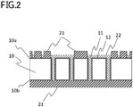
Fig. 2 is a cross-sectional view illustrating a state in which an electrolytic copper plating has been formed in gaps of a dry film resist pattern. -
Fig. 3 is a cross-sectional view illustrating a state in which a wiring pattern protective resin has been formed on a first surface of the glass core, with a support substrate being temporarily bonded thereon. -
Fig. 4 is a cross-sectional view illustrating a state in which portions of the glass core have been irradiated with a CO2 laser beam from a second surface side thereof and transformed. -
Fig. 5 is a cross-sectional view illustrating a state in which glass has been dissolved from the second surface side of the glass core. -
Fig. 6 is a cross-sectional view illustrating a state in which a wiring pattern has been formed on the second surface of the glass core and a wiring pattern protective resin has been further formed thereon. -
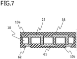
Fig. 7 is a cross-sectional view illustrating a glass core device cut out by dicing the wiring pattern protective resin in a device size and separated from a carrier substrate. -
Fig. 8 is a cross-sectional view illustrating two glass cores which are respectively provided with wiring pattern protective resins on the first surfaces thereof and are temporarily bonded together via a carrier substrate so that the first surfaces face each other. - With reference to the accompanying drawings, some embodiments of the present invention will be described.
Figs. 1 to 7 each show a process of producing a glass core device according to a first embodiment. In the present specification, the term through-glass vias (TGVs) refers to a wiring pattern formed through a glass core; however, herein, the term also refers to through holes prior to forming a wiring pattern. - First,
TGVs 11 are formed in aglass core 10 as shown inFig. 1 . The method of formingTGVs 11 may be laser beam irradiation or chemical treatment using hydrofluoric acid but is not limited thereto. Aseed layer 12 for supplying electrical power for electroplating is formed on surfaces of theglass core 10 having a thickness of 300 µm in which TGVs 11 have been formed. Theseed layer 12 for supplying electrical power can be formed by Ti/Cu sputtering or electroless copper plating. Theseed layer 12 is formed at least on afirst surface 10a and insideTGVs 11. When forming theseed layer 12 by Ti/Cu sputtering inTGVs 11 having a small diameter, it is preferred that sputtering is performed from both sides of theglass core 10 because theseed layer 12 can be formed across the inner surface of each TGV. - Next, as shown in
Fig. 2 , a layer of aphotoresist 21 of a desired pattern is formed on thefirst surface 10a and asecond surface 10b of theglass core 10. As a material for thephotoresist 21, a dry film resist is typically used in many cases. Herein, however, a direct drawing type photoresist RD-1225 (product name) manufactured by Hitachi Chemical Company, Ltd. is laminated on both surfaces of theglass core 10. Subsequently, a desired pattern is drawn on thefirst surface 10a, followed by development, to expose theseed layer 12 formed in step 1. Electrical power is then supplied to the exposed seed layer to form an electrolytic copper plating 22 with a thickness of 2 µm to 10 µm. - As shown in
Fig. 3 , unwanted dry film resist is separated and theseed layer 12 is etched away to thereby form a desired copper wiring pattern on thefirst surface 10a of theglass core 10. Then, a coating of a wiring pattern protective insulatingresin 33 is formed on the copper wiring pattern. Furthermore, acarrier substrate 31 is bonded to thefirst surface 10a of theglass core 10 via an adhesive 32 for temporary bonding. - In the present embodiment, as shown in
Fig. 3 , the copper wiring pattern is formed as a single layer. However, the copper wiring pattern may be formed as a buildup multilayer wiring pattern by forming vias in the wiring pattern protective insulatingresin 33 and further forming a copper wiring pattern thereon. The present embodiment is described taking an example in which an epoxy substrate is separately prepared as acarrier substrate 31. However, the carrier substrate may be a glass substrate or a metal plate, such as SUS, as long as the substrate is rigid and smooth. - As shown in
Fig. 4 , theglass core 10 is irradiated with a femtosecond laser beam LB in an X-Y matrix so that the irradiated portions are each transformed in a shape of a tapered groove, so that theglass core 10 can be diced to a size required as a glass core device. The glass portions (the portions each transformed in a shape of a tapered groove) 41 irradiated with the femtosecond laser beam LB exhibit improved solubility in a glass-dissolving solution such as of hydrofluoric acid. The femtosecond laser used herein is preferred to have an output of 0.1 µJ or more, and more preferably 0.4 µJ or more. The present embodiment is described taking an example of using a femtosecond laser. However, any laser, e.g., a picosecond laser, may be used as long as it is a pulsed laser. - The
second surface 10b is flatly ground by 100 µm to 150 µm. Thus, a thin glass core device can be formed. Theglass core 10 is then immersed in a glass-dissolving solution such as of hydrofluoric acid, or a glass-dissolving solution is sprayed onto thesecond surface 10b, to preferentially dissolve theglass portions 41 that have been transformed by the femtosecond laser processing in step 4, while also dissolving thesecond surface 10b of the glass core even more by 1 µm to 5 µm. As a result, asecond surface 10c as shown inFig. 5 is formed. Thus, ends of the copper wiring pattern embedded inTGVs 11 protrude by 1 µm to 5 µm. In this processing, microcracked portions produced on the femtosecond laser processed surfaces and the groundsecond surface 10b are dissolved and removed, as an effective side benefit of the glass-dissolving solution, to thereby form thesecond surface 10c. Therefore, theglass core 10 is prevented from cracking in the subsequent steps. - Next, as shown in
Fig. 6 , anotherseed layer 12 for electrical power supply is formed on thesecond surface 10c of theglass core 10 as in steps 1 and 2. Thereafter, a pattern of a dry film resist (not shown) is formed on thesecond surface 10c of theglass core 10 to connect between the ends of the copper wiring pattern protruded from thesecond surface 10c. Furthermore, electrical power is supplied to theseed layer 12 to form an electrolytic copper plating 61 with a thickness of 2 µm to 10 µm and then unwanted dry film resist is separated, followed by etching away the exposedseed layer 12. - The electrolytic copper plating 61 provides a copper plating structure covering the copper wiring pattern exposed from the
second surface 10c of theglass core 10. Since the electrolytic copper plating 61 is deposited from theseed layer 12 and the copper wiring pattern which are not flush with thesecond surface 10c of theglass core 10, the copper cannot separate from thesecond surface 10c of theglass core 10. Furthermore, thesecond surface 10c of theglass core 10 is covered with an outer protective layer (protective resin) 62 such as of a solder resist, for protection. If an external connection terminal or the like is required to be connected, anopening 63 may be formed to expose the copper pattern. - Next, the outer
protective layer 62 such as of a solder resist is diced in an X-Y matrix at the positions (at the centers of the respective grooves resulting from transformation by the laser beam) indicated by the dash-dot lines inFig. 6 to cut out glass core devices. Then, the glass core devices are separated from thecarrier substrate 31, to which they have been temporarily bonded in step 3, to complete a glass core device as shown inFig. 7 . In this case, it is preferred that theseed layer 12 and the electrolytic copper plating 61 are ensured to remain on side faces 10d of theglass core 10 shown inFig. 6 . The glass core devices herein have been cut out together with thecarrier substrate 31 by dicing. However, the glass core devices alone may be cut out by dicing without cutting thecarrier substrate 31. In this case, glass core devices remain adhered to thecarrier substrate 31 to improve handleability during transportation or storage. - As in the processing of the first embodiment, two intermediate products of the same size are prepared referring to
Fig. 2 . Then, as shown inFig. 3 , seed layers 12 are etched away to form desired copper wiring patterns on the respectivefirst surfaces 10a of the twoglass cores 10, which are then coated with a wiring pattern protective insulatingresin 33. Next, in the present embodiment, an adhesive 32 for temporary bonding is applied, as shown inFig. 8 , to both surfaces of acarrier substrate 31. Then, thefirst surfaces 10a of the twoglass cores 10 are bonded to thecarrier substrate 31 so as to face each other.
The processing after that is the same as in the embodiment described above. - The first embodiment described above has shown an example of producing a glass core device, in which the number of glass core devices correspond to the number of segments of a
carrier substrate 31. However, in the second embodiment, steps 4 to 7 can be performed on both surfaces of onecarrier substrate 31. Therefore, glass core devices that have twice the number of segments of thecarrier substrate 31 can be prepared, i.e., production efficiency is improved approximately twofold by simple calculations. - In the present embodiment described above, the intermediate products have been bonded together via a
carrier substrate 31. However, two intermediate products may be bonded together via only one adhesive layer for temporary bonding, without using a carrier substrate. - The present embodiment can provide a glass core device, at low cost, having reliability and sufficient mechanical strength by flattening and protecting the surfaces of a glass core in which TGVs are formed, and a method of producing the glass core device. Also, in the present embodiment, microcracked portions on the surfaces of a glass core due to polishing/grinding, or due to transportation or rack storage with the glass-core-device-producing equipment, or due to chemical treatment with strong acid or strong alkali, are dissolved and removed in a glass-dissolving solution. Then, a protective resin, such as an insulating liquid resin or a dry film material, is applied to the exposed glass core and the wiring pattern to prevent the glass core from being exposed to the outside. Thus, product quality is improved.
- Furthermore, in the present embodiment, a glass material with a thickness of 800 µm or more is thinned, so that the glass core will finally have a preferred thickness of 20 µm or more and 800 µm or less. The glass core with such a thickness can alleviate the stress by gradual annealing, which is applied when forming a copper wiring pattern or an insulating resin layer on the glass core. If the glass core material with the above thickness is used alone, the glass core may crack during the production process. Therefore, it is desired that a carrier substrate is bonded, as in the present embodiment, to the first surface of the glass core via a separable adhesive, and then separated after producing glass core devices.
- In the present embodiment, the second surface of the glass core is treated with hydrofluoric acid. This treatment can remove the microcracked portions caused due to grinding for thinning the glass core, or due to transportation contact or rack storage contact, or due to chemical treatment with strong acid or strong alkali, or the like. By undergoing hydrofluoric acid treatment, the glass core can have a surface roughness Ra of 20 nm or less (according to ISO25178-604, and which can be measured by using a NewView 8200 (product name) manufactured by Zygo Corporation), so that the glass core is prevented from being broken starting from the microcracks. It should be noted that the surface roughness Ra of a glass core can be measured when separating the protective resin layer from glass core devices as products.
- Furthermore, in the present embodiment, at least the outer peripheral portion of the first surface of the glass core and the side faces of the glass core are covered with a metal film and are further coated with a protective resin. If the glass core is exposed from the glass core device, the glass core may crack due to the thermal shock induced by rapid heating treatment during the process of mounting active and passive components to the glass core device or the process of soldering the device to the motherboard, e.g., a reflow process, or due to mechanical impact caused by the glass core device impacting other objects. In this regard, in the present embodiment, the side faces of the glass core (inside the grooves where the glass has been transformed by laser beam irradiation and removed by hydrofluoric acid) can be easily covered with a metal film formed by a dry film forming method, such as sputtering or deposition, or by a wet film forming method, such as metal plating. Thus, the glass core is prevented from cracking from the side faces thereof. Furthermore, by coating the side faces of the glass core with a protective resin, corrosion of the metal film can be prevented.
- Furthermore, in the present embodiment, a hydrofluoric-acid resistant protective film is laminated on the first surface of the glass core and then the second surface thereof is treated with hydrofluoric acid to reduce the thickness of the glass core. At the same time, the glass core can be cut to a desired glass-core-device size. Glass core devices generally have a rectangular parallelopiped shape with a 2 mm- to 50 mm-square bottom. Since the glass core enclosed in a glass core device is processed from the second surface side when reducing the thickness thereof, the glass core may have a truncated square pyramidal shape (i.e., tapered) in which the sides on the first surface are shorter than the sides on the second surface. To improve productivity and reduce cost, the glass core devices of the present embodiment are collectively produced by using a 300 mm-square glass material and arranging the glass core devices in a matrix.
- The present embodiment uses a glass core in which a wiring pattern is formed in TGVs and a desired multilayer wiring layer is formed on the first surface. Since glass core materials suffer from an issue of easily cracking during the production process as mentioned above, a carrier substrate is bonded to the first surface of the glass core via a separable adhesive.
- Furthermore, the glass core is linearly irradiated with a controlled femtosecond laser beam from the second surface side along division lines conforming to the glass-core-device size to transform portions of the glass core without being melted. Thus, in hydrofluoric acid treatment, the transformed linear portions of the glass core are more preferentially etched away than in the portions not irradiated with the laser beam. While the second surface of the glass core undergoes etching for thickness reduction, the portions transformed by laser beam irradiation are etched away. Thus, the glass core can be cut to a desired size.
- Furthermore, in the present embodiment, a hydrofluoric-acid resistant protective film is firstly laminated on the first surface of the glass core and then the second surface thereof undergoes hydrofluoric acid treatment to reduce the thickness of the glass core. Through this treatment, the ends of the copper wiring pattern formed in TGVs are protruded from the second surface of the glass core. This protrusion contributes to improving reliability on the second surface of the glass core when establishing connection with a wiring pattern in the later process. Thus, the hydrofluoric acid treatment is preferred to be performed such that the ends of the wiring pattern in TGVs are exposed at a height of 1 µm to 15 µm from the second surface of the glass core.
- In the present embodiment, when forming a wiring pattern on the second surface of the glass core, a metal wiring pattern is formed, connecting between the ends of the TGV-embedded wiring pattern protruded from the second surface, while also forming a metal film in the grooves where the glass core has been transformed by laser beam irradiation and etched away as mentioned above. By forming a metal film at the outer peripheral portion, breakage is prevented from occurring from the side faces of the truncated square pyramid of the glass core. If the metal wiring pattern is formed only on the first and second surfaces of the glass core, breakage is likely to occur from the side faces of the truncated square pyramid of the glass core due to tensile stress induced by self-annealing or due to expansion and contraction caused by reflow heat treatment when mounting the device. However, such disadvantages can be eliminated by the present embodiment.
- By forming a metal adhesion-enhancing layer by sputtering or electroless plating on the outer peripheral portion of the glass core and by covering the layer with an electrolytic plating to increase the thickness, the occurrence of breakage is prevented or minimized. The metal adhesion-enhancing layer is preferred to be provided by forming a film of Ti, Ni, Cu or the like for use as a seed layer for electrolytic plating. The electrolytic plating bath is preferred to be an electrolytic copper plating bath from the perspective of improving working efficiency for simultaneously forming a wiring pattern on the second surface, with films on the side faces of the truncated square pyramid of the glass core.
- In the present embodiment, it is preferred that, in each of the glass core devices cut out with a desired size, the second surface and the side faces of the truncated square pyramid of the glass core are coated with a resin, ceramic or the like to provide an outer protective layer. The outer protective layer covers and protects a total of five surfaces, including the second surface and the side faces of the truncated square pyramid of the glass core. Portions of the embedded outer protective layer are diced along the center of each groove that has been formed in the glass core by transforming a portion of the glass core by femtosecond laser beam irradiation and removing the transformed portion with hydrofluoric acid, to finally cut out glass core devices. The cut out glass core devices each have a rectangular parallelopiped shape without exposing the glass core.
- It should be noted that a buildup resin may be laminated (an insulating resin lamination layer may be formed) on the first or second surface of the glass core, followed by forming vias and a wiring layer. These processes may be repeated to provide a multilayer wiring pattern. Alternatively, the glass core device may be incorporated with a passive component by forming a capacitor, in which a high dielectric material is embedded, in the device or by forming a resistor in the device. Alternatively, the glass core device may be incorporated with an inductor by forming a coiled wiring pattern in the device.
-
- 10:
- Glass core
- 10a:
- First surface
- 10b:
- Second surface
- 11:
- TGV
- 12:
- Seed layer
- 21:
- Photoresist
- 22:
- Electrolytic copper plating
- 31:
- Carrier substrate
- 32:
- Adhesive
- 33:
- Wiring pattern protective insulating resin
- 41:
- Transformed glass portion
- 61:
- Electrolytic copper plating
- 62:
- Outer protective layer
Claims (8)
- A glass core device comprising a flat glass core having a first surface and a second surface facing away from each other, through-glass vias formed in the glass core, and a wiring pattern embedded in the through-glass vias, the first surface and the second surface of the glass core being respectively provided thereon with wiring patterns which are electrically connected via the wiring pattern embedded in the through-glass vias, characterized in that:
the glass core device is provided with a protective resin continuously covering the second surface of the glass core and side faces of the glass core. - The glass core device according to claim 1, characterized in that the glass core has a thickness of 20 µm or more and 800 µm or less.
- The glass core device according to claim 1 or 2, characterized in that the glass core has a surface roughness Ra of 20 nm or less.
- The glass core device according to any one of claims 1 to 3, characterized in that at least an outer peripheral portion of the first surface and the second surface of the glass core and the side faces of the glass core are covered with a metal film and are further coated with the protective resin.
- The glass core device according to any one of claims 1 to 4, characterized in that the glass core has a truncated square pyramidal shape, with sides on the second surface parallel to the first surface being shorter than sides on the first surface.
- The glass core device according to any one of claims 1 to 5, characterized in that portions of the wiring pattern embedded in the through-glass vias protrude from the second surface of the glass core.
- A method of producing a glass core device, characterized in that the method comprises steps of:forming through holes in a glass core having a first surface and a second surface facing away from each other;forming through-glass vias by forming a wiring pattern on the first surface of the glass core and in the through holes thereof, and sealing the first surface with an insulating resin;bonding a carrier substrate onto the first surface of the glass core;linearly irradiating the second surface of the glass core with a laser beam to transform the glass core;etching away the transformed portions of the glass core by chemical treatment to form grooves for dicing the glass core;forming a wiring pattern on the second surface of the glass core, filling the grooves with a protective resin, and sealing the second surface with the protective resin; andcutting the protective resin filled in the grooves.
- The method of producing a glass core device according to claim 7, characterized in that, in the step of etching away the transformed portions of the glass core by chemical treatment to form grooves for dicing the glass core:exposed portions of the second surface of the glass core are also etched to reduce thickness of the glass core and protrude the wiring pattern in the through-glass vias from the second surface; anda wiring pattern is formed on the second surface so as to be connected to the protruded wiring pattern in the through-glass vias.
Applications Claiming Priority (2)
| Application Number | Priority Date | Filing Date | Title |
|---|---|---|---|
| JP2018013620A JP7106875B2 (en) | 2018-01-30 | 2018-01-30 | Glass core device manufacturing method |
| PCT/JP2019/001590 WO2019151003A1 (en) | 2018-01-30 | 2019-01-21 | Glass core device, and method for manufacturing same |
Publications (3)
| Publication Number | Publication Date |
|---|---|
| EP3749066A1 true EP3749066A1 (en) | 2020-12-09 |
| EP3749066A4 EP3749066A4 (en) | 2021-03-17 |
| EP3749066B1 EP3749066B1 (en) | 2026-01-07 |
Family
ID=67478211
Family Applications (1)
| Application Number | Title | Priority Date | Filing Date |
|---|---|---|---|
| EP19747585.8A Active EP3749066B1 (en) | 2018-01-30 | 2019-01-21 | Method of producing a glass core device |
Country Status (5)
| Country | Link |
|---|---|
| US (1) | US11764138B2 (en) |
| EP (1) | EP3749066B1 (en) |
| JP (1) | JP7106875B2 (en) |
| CN (1) | CN111903196B (en) |
| WO (1) | WO2019151003A1 (en) |
Families Citing this family (14)
| Publication number | Priority date | Publication date | Assignee | Title |
|---|---|---|---|---|
| JP2023015410A (en) * | 2019-11-07 | 2023-02-01 | 株式会社エンプラス | Glass plate having through-hole pattern formed therein, manufacturing method therefor, and micro-channel chip |
| JP7439497B2 (en) * | 2019-12-20 | 2024-02-28 | Toppanホールディングス株式会社 | Glass core multilayer wiring board manufacturing method, glass core multilayer wiring board and high frequency module board |
| JP7512594B2 (en) * | 2020-01-10 | 2024-07-09 | Toppanホールディングス株式会社 | Circuit Board |
| JP2022151782A (en) * | 2021-03-23 | 2022-10-07 | 凸版印刷株式会社 | Glass substrate and glass-core multilayer wiring board |
| US20230087838A1 (en) * | 2021-09-20 | 2023-03-23 | Intel Corporation | Protective coating on an edge of a glass core |
| US20230197592A1 (en) * | 2021-12-16 | 2023-06-22 | Intel Corporation | Power delivery techniques for glass substrate with high density signal vias |
| CN114521072B (en) * | 2022-02-11 | 2023-03-10 | 北京华镁钛科技有限公司 | Counter bore thin copper surface process circuit board pressing device and process |
| WO2024004566A1 (en) * | 2022-07-01 | 2024-01-04 | Toppanホールディングス株式会社 | Glass core laminate structure and production method for glass core laminate structure |
| US20240177918A1 (en) * | 2022-11-29 | 2024-05-30 | Intel Corporation | Glass embedded true air core inductors |
| CN116403913A (en) * | 2023-03-27 | 2023-07-07 | 上海美维科技有限公司 | FCBGA packaging core board, packaging substrate and preparation method thereof |
| US20250192059A1 (en) * | 2023-12-06 | 2025-06-12 | Intel Corporation | Embedded bridge with through silicon via bonding architectures |
| WO2025142478A1 (en) | 2023-12-28 | 2025-07-03 | Toppanホールディングス株式会社 | Multilayer wiring board, method for manufacturing multilayer wiring board, and multilayer wiring base board |
| CN117894688B (en) * | 2024-01-15 | 2026-04-17 | 湖北通格微电路科技有限公司 | Packaging substrate fabrication method, packaging substrate |
| JP7670251B1 (en) | 2024-01-31 | 2025-04-30 | 株式会社レゾナック | Method for manufacturing glass substrate with conductive vias |
Family Cites Families (27)
| Publication number | Priority date | Publication date | Assignee | Title |
|---|---|---|---|---|
| TW323432B (en) * | 1995-04-28 | 1997-12-21 | Victor Company Of Japan | |
| US6492600B1 (en) * | 1999-06-28 | 2002-12-10 | International Business Machines Corporation | Laminate having plated microvia interconnects and method for forming the same |
| JP2003257895A (en) * | 2002-02-28 | 2003-09-12 | Mitsubishi Electric Corp | Wafer on which semiconductor chip is mounted and method of manufacturing the same |
| JP2004165312A (en) * | 2002-11-12 | 2004-06-10 | Sanyo Electric Co Ltd | Semiconductor integrated device and method of manufacturing the same |
| EP1990125B1 (en) * | 2006-02-22 | 2011-10-12 | Nippon Sheet Glass Company, Limited | Glass processing method using laser |
| JP2007318058A (en) * | 2006-04-27 | 2007-12-06 | Murata Mfg Co Ltd | Electronic component and manufacturing method thereof |
| US8058960B2 (en) * | 2007-03-27 | 2011-11-15 | Alpha And Omega Semiconductor Incorporated | Chip scale power converter package having an inductor substrate |
| JP5193809B2 (en) * | 2008-11-05 | 2013-05-08 | 新光電気工業株式会社 | Wiring board and manufacturing method thereof |
| JP4978974B1 (en) * | 2011-03-28 | 2012-07-18 | Smk株式会社 | Glass substrate for touch panel and manufacturing method thereof |
| US20130050228A1 (en) * | 2011-08-30 | 2013-02-28 | Qualcomm Mems Technologies, Inc. | Glass as a substrate material and a final package for mems and ic devices |
| US20130207745A1 (en) | 2012-02-13 | 2013-08-15 | Qualcomm Incorporated | 3d rf l-c filters using through glass vias |
| US9082764B2 (en) * | 2012-03-05 | 2015-07-14 | Corning Incorporated | Three-dimensional integrated circuit which incorporates a glass interposer and method for fabricating the same |
| JP6038517B2 (en) * | 2012-07-13 | 2016-12-07 | 新光電気工業株式会社 | Wiring board and manufacturing method thereof |
| US9425761B2 (en) * | 2013-05-31 | 2016-08-23 | Qualcomm Incorporated | High pass filters and low pass filters using through glass via technology |
| KR101548816B1 (en) * | 2013-11-11 | 2015-08-31 | 삼성전기주식회사 | Printed circuit board and method of manufacturing the same |
| JP2015156427A (en) * | 2014-02-20 | 2015-08-27 | アイシン精機株式会社 | Glass processed component, manufacturing method thereof, electronic device and manufacturing method thereof |
| KR101580287B1 (en) * | 2014-05-02 | 2015-12-24 | 삼성전기주식회사 | Printed circuit board, printed circuit board strip and manufacturing method thereof |
| KR102396144B1 (en) * | 2014-08-04 | 2022-05-10 | 엘지이노텍 주식회사 | Method for Manufacturing Glass Interposer |
| CN106795044A (en) * | 2014-10-03 | 2017-05-31 | 日本板硝子株式会社 | Manufacturing method of glass substrate with through-hole electrode and glass substrate |
| KR101629435B1 (en) * | 2014-11-10 | 2016-06-10 | 삼성전기주식회사 | Printed circuit board and manufacturing method thereof |
| JP2016111221A (en) * | 2014-12-08 | 2016-06-20 | 日本特殊陶業株式会社 | Method of manufacturing wiring board and wiring board |
| KR20160080526A (en) * | 2014-12-29 | 2016-07-08 | 삼성전기주식회사 | Printed circuit board and method of manufacturing the same |
| US9859159B2 (en) * | 2015-03-10 | 2018-01-02 | Unimicron Technology Corp. | Interconnection structure and manufacturing method thereof |
| US10090255B2 (en) * | 2016-01-29 | 2018-10-02 | Globalfoundries Inc. | Dicing channels for glass interposers |
| JP6672859B2 (en) * | 2016-02-09 | 2020-03-25 | 凸版印刷株式会社 | Method of manufacturing core substrate for printed circuit board, method of manufacturing printed circuit board, and method of manufacturing semiconductor device |
| US10134657B2 (en) * | 2016-06-29 | 2018-11-20 | Corning Incorporated | Inorganic wafer having through-holes attached to semiconductor wafer |
| US10044390B2 (en) * | 2016-07-21 | 2018-08-07 | Qualcomm Incorporated | Glass substrate including passive-on-glass device and semiconductor die |
-
2018
- 2018-01-30 JP JP2018013620A patent/JP7106875B2/en active Active
-
2019
- 2019-01-21 CN CN201980009996.3A patent/CN111903196B/en active Active
- 2019-01-21 WO PCT/JP2019/001590 patent/WO2019151003A1/en not_active Ceased
- 2019-01-21 EP EP19747585.8A patent/EP3749066B1/en active Active
-
2020
- 2020-07-24 US US16/938,144 patent/US11764138B2/en active Active
Also Published As
| Publication number | Publication date |
|---|---|
| EP3749066B1 (en) | 2026-01-07 |
| US20200357734A1 (en) | 2020-11-12 |
| CN111903196A (en) | 2020-11-06 |
| JP2019134016A (en) | 2019-08-08 |
| WO2019151003A1 (en) | 2019-08-08 |
| CN111903196B (en) | 2024-07-02 |
| US11764138B2 (en) | 2023-09-19 |
| JP7106875B2 (en) | 2022-07-27 |
| EP3749066A4 (en) | 2021-03-17 |
Similar Documents
| Publication | Publication Date | Title |
|---|---|---|
| EP3749066B1 (en) | Method of producing a glass core device | |
| US11406025B2 (en) | Glass wiring board, method for manufacturing the same, and semiconductor device | |
| US11006516B2 (en) | Wiring board, semiconductor device, and method of manufacturing wiring board | |
| CN103314649B (en) | Method and associated apparatus for transferring and electrically bonding high density multilayer thin films to circuitized and flexible organic substrates | |
| EP3138120B1 (en) | Etch back processes of bonding material for the manufacture of through-glass vias | |
| EP1261021A2 (en) | Method of production of circuit board, semiconductor device, and plating system | |
| TW201816900A (en) | Electronic package of glass substrate and forming method thereof | |
| JP4630110B2 (en) | Manufacturing method of electronic parts | |
| KR20040084708A (en) | Method of production of multilayer circuit board with built-in semiconductor chip | |
| TWI442528B (en) | Semiconductor package manufacturing method | |
| US20250125272A1 (en) | Glass core laminate structure and production method for glass core laminate structure | |
| TW202431908A (en) | Wiring board | |
| WO2001080299A1 (en) | Semiconductor device and fabrication method therefor | |
| KR100927778B1 (en) | Semiconductor Package Manufacturing Method | |
| JP2016143725A (en) | Printed wiring board and manufacturing method thereof | |
| KR102799946B1 (en) | Method of manufacturing the printed circuit board embedded with wafer level component | |
| JP5524680B2 (en) | Manufacturing method of capacitor for wiring board | |
| KR20170067180A (en) | Method of fabricating a circuit board | |
| JP7182084B2 (en) | Penetration electrode substrate and manufacturing method thereof | |
| KR20140080112A (en) | Metal core substrate and manufacturing method thereof | |
| CN113871304A (en) | A kind of manufacturing method of coreless substrate | |
| CN119560477A (en) | Glass substrate, method for manufacturing glass substrate, packaging method and electronic device | |
| JP2023009747A (en) | Multilayer wiring board and manufacturing method thereof | |
| JP2001177047A (en) | Manufacturing method of stacked semiconductor device | |
| JP2007227834A (en) | Semiconductor device and manufacturing method thereof |
Legal Events
| Date | Code | Title | Description |
|---|---|---|---|
| STAA | Information on the status of an ep patent application or granted ep patent |
Free format text: STATUS: THE INTERNATIONAL PUBLICATION HAS BEEN MADE |
|
| PUAI | Public reference made under article 153(3) epc to a published international application that has entered the european phase |
Free format text: ORIGINAL CODE: 0009012 |
|
| STAA | Information on the status of an ep patent application or granted ep patent |
Free format text: STATUS: REQUEST FOR EXAMINATION WAS MADE |
|
| 17P | Request for examination filed |
Effective date: 20200702 |
|
| AK | Designated contracting states |
Kind code of ref document: A1 Designated state(s): AL AT BE BG CH CY CZ DE DK EE ES FI FR GB GR HR HU IE IS IT LI LT LU LV MC MK MT NL NO PL PT RO RS SE SI SK SM TR |
|
| AX | Request for extension of the european patent |
Extension state: BA ME |
|
| A4 | Supplementary search report drawn up and despatched |
Effective date: 20210215 |
|
| RIC1 | Information provided on ipc code assigned before grant |
Ipc: H05K 3/42 20060101ALI20210209BHEP Ipc: H05K 3/10 20060101ALN20210209BHEP Ipc: H05K 3/46 20060101ALN20210209BHEP Ipc: H05K 3/00 20060101ALI20210209BHEP Ipc: H05K 3/28 20060101AFI20210209BHEP Ipc: H05K 1/16 20060101ALN20210209BHEP |
|
| DAV | Request for validation of the european patent (deleted) | ||
| DAX | Request for extension of the european patent (deleted) | ||
| RIN1 | Information on inventor provided before grant (corrected) |
Inventor name: AKUTAGAWA, YOSHITO Inventor name: HITSUOKA, YASUYUKI Inventor name: KOGA, OSAMU |
|
| STAA | Information on the status of an ep patent application or granted ep patent |
Free format text: STATUS: EXAMINATION IS IN PROGRESS |
|
| 17Q | First examination report despatched |
Effective date: 20221222 |
|
| REG | Reference to a national code |
Ref country code: DE Ref legal event code: R079 Free format text: PREVIOUS MAIN CLASS: H05K0001020000 Ipc: H05K0003280000 Ref country code: DE Ref legal event code: R079 Ref document number: 602019080116 Country of ref document: DE Free format text: PREVIOUS MAIN CLASS: H05K0001020000 Ipc: H05K0003280000 |
|
| GRAP | Despatch of communication of intention to grant a patent |
Free format text: ORIGINAL CODE: EPIDOSNIGR1 |
|
| STAA | Information on the status of an ep patent application or granted ep patent |
Free format text: STATUS: GRANT OF PATENT IS INTENDED |
|
| RIC1 | Information provided on ipc code assigned before grant |
Ipc: H05K 3/28 20060101AFI20250930BHEP Ipc: H05K 3/42 20060101ALI20250930BHEP Ipc: H05K 3/00 20060101ALI20250930BHEP Ipc: H01F 17/00 20060101ALI20250930BHEP Ipc: H01F 41/04 20060101ALI20250930BHEP Ipc: H05K 1/16 20060101ALN20250930BHEP Ipc: H05K 3/10 20060101ALN20250930BHEP Ipc: H05K 3/46 20060101ALN20250930BHEP |
|
| INTG | Intention to grant announced |
Effective date: 20251015 |
|
| GRAS | Grant fee paid |
Free format text: ORIGINAL CODE: EPIDOSNIGR3 |
|
| GRAA | (expected) grant |
Free format text: ORIGINAL CODE: 0009210 |
|
| STAA | Information on the status of an ep patent application or granted ep patent |
Free format text: STATUS: THE PATENT HAS BEEN GRANTED |
|
| AK | Designated contracting states |
Kind code of ref document: B1 Designated state(s): AL AT BE BG CH CY CZ DE DK EE ES FI FR GB GR HR HU IE IS IT LI LT LU LV MC MK MT NL NO PL PT RO RS SE SI SK SM TR |
|
| REG | Reference to a national code |
Ref country code: CH Ref legal event code: F10 Free format text: ST27 STATUS EVENT CODE: U-0-0-F10-F00 (AS PROVIDED BY THE NATIONAL OFFICE) Effective date: 20260107 Ref country code: GB Ref legal event code: FG4D |
|
| REG | Reference to a national code |
Ref country code: DE Ref legal event code: R096 Ref document number: 602019080116 Country of ref document: DE |
|
| REG | Reference to a national code |
Ref country code: IE Ref legal event code: FG4D |
|
| PGFP | Annual fee paid to national office [announced via postgrant information from national office to epo] |
Ref country code: GB Payment date: 20260216 Year of fee payment: 8 |
|
| PGFP | Annual fee paid to national office [announced via postgrant information from national office to epo] |
Ref country code: DE Payment date: 20260211 Year of fee payment: 8 |
|
| PGFP | Annual fee paid to national office [announced via postgrant information from national office to epo] |
Ref country code: FR Payment date: 20260225 Year of fee payment: 8 |
|
| REG | Reference to a national code |
Ref country code: NL Ref legal event code: MP Effective date: 20260107 |
|
| PG25 | Lapsed in a contracting state [announced via postgrant information from national office to epo] |
Ref country code: NL Free format text: LAPSE BECAUSE OF FAILURE TO SUBMIT A TRANSLATION OF THE DESCRIPTION OR TO PAY THE FEE WITHIN THE PRESCRIBED TIME-LIMIT Effective date: 20260107 |
|
| REG | Reference to a national code |
Ref country code: AT Ref legal event code: MK05 Ref document number: 1876475 Country of ref document: AT Kind code of ref document: T Effective date: 20260107 |
|
| PG25 | Lapsed in a contracting state [announced via postgrant information from national office to epo] |
Ref country code: RS Free format text: LAPSE BECAUSE OF FAILURE TO SUBMIT A TRANSLATION OF THE DESCRIPTION OR TO PAY THE FEE WITHIN THE PRESCRIBED TIME-LIMIT Effective date: 20260407 |
|
| PG25 | Lapsed in a contracting state [announced via postgrant information from national office to epo] |
Ref country code: ES Free format text: LAPSE BECAUSE OF FAILURE TO SUBMIT A TRANSLATION OF THE DESCRIPTION OR TO PAY THE FEE WITHIN THE PRESCRIBED TIME-LIMIT Effective date: 20260107 |
|
| PG25 | Lapsed in a contracting state [announced via postgrant information from national office to epo] |
Ref country code: PL Free format text: LAPSE BECAUSE OF FAILURE TO SUBMIT A TRANSLATION OF THE DESCRIPTION OR TO PAY THE FEE WITHIN THE PRESCRIBED TIME-LIMIT Effective date: 20260107 |
|
| PG25 | Lapsed in a contracting state [announced via postgrant information from national office to epo] |
Ref country code: GR Free format text: LAPSE BECAUSE OF FAILURE TO SUBMIT A TRANSLATION OF THE DESCRIPTION OR TO PAY THE FEE WITHIN THE PRESCRIBED TIME-LIMIT Effective date: 20260408 |
|
| REG | Reference to a national code |
Ref country code: LT Ref legal event code: MG9D |
|
| PG25 | Lapsed in a contracting state [announced via postgrant information from national office to epo] |
Ref country code: LT Free format text: LAPSE BECAUSE OF FAILURE TO SUBMIT A TRANSLATION OF THE DESCRIPTION OR TO PAY THE FEE WITHIN THE PRESCRIBED TIME-LIMIT Effective date: 20260107 |
|
| PG25 | Lapsed in a contracting state [announced via postgrant information from national office to epo] |
Ref country code: NO Free format text: LAPSE BECAUSE OF FAILURE TO SUBMIT A TRANSLATION OF THE DESCRIPTION OR TO PAY THE FEE WITHIN THE PRESCRIBED TIME-LIMIT Effective date: 20260407 |
|
| PG25 | Lapsed in a contracting state [announced via postgrant information from national office to epo] |
Ref country code: FI Free format text: LAPSE BECAUSE OF FAILURE TO SUBMIT A TRANSLATION OF THE DESCRIPTION OR TO PAY THE FEE WITHIN THE PRESCRIBED TIME-LIMIT Effective date: 20260107 Ref country code: SE Free format text: LAPSE BECAUSE OF FAILURE TO SUBMIT A TRANSLATION OF THE DESCRIPTION OR TO PAY THE FEE WITHIN THE PRESCRIBED TIME-LIMIT Effective date: 20260107 Ref country code: AT Free format text: LAPSE BECAUSE OF FAILURE TO SUBMIT A TRANSLATION OF THE DESCRIPTION OR TO PAY THE FEE WITHIN THE PRESCRIBED TIME-LIMIT Effective date: 20260107 |
|
| PG25 | Lapsed in a contracting state [announced via postgrant information from national office to epo] |
Ref country code: HR Free format text: LAPSE BECAUSE OF FAILURE TO SUBMIT A TRANSLATION OF THE DESCRIPTION OR TO PAY THE FEE WITHIN THE PRESCRIBED TIME-LIMIT Effective date: 20260107 |
|
| PG25 | Lapsed in a contracting state [announced via postgrant information from national office to epo] |
Ref country code: IS Free format text: LAPSE BECAUSE OF FAILURE TO SUBMIT A TRANSLATION OF THE DESCRIPTION OR TO PAY THE FEE WITHIN THE PRESCRIBED TIME-LIMIT Effective date: 20260507 Ref country code: PT Free format text: LAPSE BECAUSE OF FAILURE TO SUBMIT A TRANSLATION OF THE DESCRIPTION OR TO PAY THE FEE WITHIN THE PRESCRIBED TIME-LIMIT Effective date: 20260507 |
|
| PG25 | Lapsed in a contracting state [announced via postgrant information from national office to epo] |
Ref country code: LV Free format text: LAPSE BECAUSE OF FAILURE TO SUBMIT A TRANSLATION OF THE DESCRIPTION OR TO PAY THE FEE WITHIN THE PRESCRIBED TIME-LIMIT Effective date: 20260107 |
|
| PG25 | Lapsed in a contracting state [announced via postgrant information from national office to epo] |
Ref country code: BG Free format text: LAPSE BECAUSE OF FAILURE TO SUBMIT A TRANSLATION OF THE DESCRIPTION OR TO PAY THE FEE WITHIN THE PRESCRIBED TIME-LIMIT Effective date: 20260107 |