EP3748673A2 - Elektronische vorrichtung mit einer eine erste anschlussfläche mit einer zweiten anschlussfläche verbindenden und in einer vertiefung in der ersten anschlussfläche sinkenden leitenden partikel - Google Patents
Elektronische vorrichtung mit einer eine erste anschlussfläche mit einer zweiten anschlussfläche verbindenden und in einer vertiefung in der ersten anschlussfläche sinkenden leitenden partikel Download PDFInfo
- Publication number
- EP3748673A2 EP3748673A2 EP20169739.8A EP20169739A EP3748673A2 EP 3748673 A2 EP3748673 A2 EP 3748673A2 EP 20169739 A EP20169739 A EP 20169739A EP 3748673 A2 EP3748673 A2 EP 3748673A2
- Authority
- EP
- European Patent Office
- Prior art keywords
- pad
- conductive
- recess
- electronic device
- disposed
- Prior art date
- Legal status (The legal status is an assumption and is not a legal conclusion. Google has not performed a legal analysis and makes no representation as to the accuracy of the status listed.)
- Withdrawn
Links
Images





Classifications
-
- H—ELECTRICITY
- H10—SEMICONDUCTOR DEVICES; ELECTRIC SOLID-STATE DEVICES NOT OTHERWISE PROVIDED FOR
- H10W—GENERIC PACKAGES, INTERCONNECTIONS, CONNECTORS OR OTHER CONSTRUCTIONAL DETAILS OF DEVICES COVERED BY CLASS H10
- H10W74/00—Encapsulations, e.g. protective coatings
- H10W74/10—Encapsulations, e.g. protective coatings characterised by their shape or disposition
- H10W74/111—Encapsulations, e.g. protective coatings characterised by their shape or disposition the semiconductor body being completely enclosed
- H10W74/127—Encapsulations, e.g. protective coatings characterised by their shape or disposition the semiconductor body being completely enclosed characterised by arrangements for sealing or adhesion
-
- H—ELECTRICITY
- H10—SEMICONDUCTOR DEVICES; ELECTRIC SOLID-STATE DEVICES NOT OTHERWISE PROVIDED FOR
- H10W—GENERIC PACKAGES, INTERCONNECTIONS, CONNECTORS OR OTHER CONSTRUCTIONAL DETAILS OF DEVICES COVERED BY CLASS H10
- H10W72/00—Interconnections or connectors in packages
- H10W72/071—Connecting or disconnecting
- H10W72/073—Connecting or disconnecting of die-attach connectors
-
- H—ELECTRICITY
- H10—SEMICONDUCTOR DEVICES; ELECTRIC SOLID-STATE DEVICES NOT OTHERWISE PROVIDED FOR
- H10W—GENERIC PACKAGES, INTERCONNECTIONS, CONNECTORS OR OTHER CONSTRUCTIONAL DETAILS OF DEVICES COVERED BY CLASS H10
- H10W90/00—Package configurations
- H10W90/701—Package configurations characterised by the relative positions of pads or connectors relative to package parts
-
- H—ELECTRICITY
- H10—SEMICONDUCTOR DEVICES; ELECTRIC SOLID-STATE DEVICES NOT OTHERWISE PROVIDED FOR
- H10W—GENERIC PACKAGES, INTERCONNECTIONS, CONNECTORS OR OTHER CONSTRUCTIONAL DETAILS OF DEVICES COVERED BY CLASS H10
- H10W70/00—Package substrates; Interposers; Redistribution layers [RDL]
- H10W70/60—Insulating or insulated package substrates; Interposers; Redistribution layers
- H10W70/62—Insulating or insulated package substrates; Interposers; Redistribution layers characterised by their interconnections
- H10W70/65—Shapes or dispositions of interconnections
-
- H—ELECTRICITY
- H10—SEMICONDUCTOR DEVICES; ELECTRIC SOLID-STATE DEVICES NOT OTHERWISE PROVIDED FOR
- H10W—GENERIC PACKAGES, INTERCONNECTIONS, CONNECTORS OR OTHER CONSTRUCTIONAL DETAILS OF DEVICES COVERED BY CLASS H10
- H10W72/00—Interconnections or connectors in packages
- H10W72/071—Connecting or disconnecting
- H10W72/072—Connecting or disconnecting of bump connectors
-
- H—ELECTRICITY
- H10—SEMICONDUCTOR DEVICES; ELECTRIC SOLID-STATE DEVICES NOT OTHERWISE PROVIDED FOR
- H10W—GENERIC PACKAGES, INTERCONNECTIONS, CONNECTORS OR OTHER CONSTRUCTIONAL DETAILS OF DEVICES COVERED BY CLASS H10
- H10W72/00—Interconnections or connectors in packages
- H10W72/20—Bump connectors, e.g. solder bumps or copper pillars; Dummy bumps; Thermal bumps
-
- H—ELECTRICITY
- H10—SEMICONDUCTOR DEVICES; ELECTRIC SOLID-STATE DEVICES NOT OTHERWISE PROVIDED FOR
- H10W—GENERIC PACKAGES, INTERCONNECTIONS, CONNECTORS OR OTHER CONSTRUCTIONAL DETAILS OF DEVICES COVERED BY CLASS H10
- H10W72/00—Interconnections or connectors in packages
- H10W72/30—Die-attach connectors
-
- H—ELECTRICITY
- H10—SEMICONDUCTOR DEVICES; ELECTRIC SOLID-STATE DEVICES NOT OTHERWISE PROVIDED FOR
- H10W—GENERIC PACKAGES, INTERCONNECTIONS, CONNECTORS OR OTHER CONSTRUCTIONAL DETAILS OF DEVICES COVERED BY CLASS H10
- H10W72/00—Interconnections or connectors in packages
- H10W72/071—Connecting or disconnecting
- H10W72/073—Connecting or disconnecting of die-attach connectors
- H10W72/07331—Connecting techniques
- H10W72/07332—Compression bonding, e.g. thermocompression bonding
-
- H—ELECTRICITY
- H10—SEMICONDUCTOR DEVICES; ELECTRIC SOLID-STATE DEVICES NOT OTHERWISE PROVIDED FOR
- H10W—GENERIC PACKAGES, INTERCONNECTIONS, CONNECTORS OR OTHER CONSTRUCTIONAL DETAILS OF DEVICES COVERED BY CLASS H10
- H10W72/00—Interconnections or connectors in packages
- H10W72/071—Connecting or disconnecting
- H10W72/073—Connecting or disconnecting of die-attach connectors
- H10W72/07351—Connecting or disconnecting of die-attach connectors characterised by changes in properties of the die-attach connectors during connecting
- H10W72/07352—Connecting or disconnecting of die-attach connectors characterised by changes in properties of the die-attach connectors during connecting changes in structures or sizes
-
- H—ELECTRICITY
- H10—SEMICONDUCTOR DEVICES; ELECTRIC SOLID-STATE DEVICES NOT OTHERWISE PROVIDED FOR
- H10W—GENERIC PACKAGES, INTERCONNECTIONS, CONNECTORS OR OTHER CONSTRUCTIONAL DETAILS OF DEVICES COVERED BY CLASS H10
- H10W72/00—Interconnections or connectors in packages
- H10W72/071—Connecting or disconnecting
- H10W72/073—Connecting or disconnecting of die-attach connectors
- H10W72/07351—Connecting or disconnecting of die-attach connectors characterised by changes in properties of the die-attach connectors during connecting
- H10W72/07353—Connecting or disconnecting of die-attach connectors characterised by changes in properties of the die-attach connectors during connecting changes in shapes
-
- H—ELECTRICITY
- H10—SEMICONDUCTOR DEVICES; ELECTRIC SOLID-STATE DEVICES NOT OTHERWISE PROVIDED FOR
- H10W—GENERIC PACKAGES, INTERCONNECTIONS, CONNECTORS OR OTHER CONSTRUCTIONAL DETAILS OF DEVICES COVERED BY CLASS H10
- H10W72/00—Interconnections or connectors in packages
- H10W72/071—Connecting or disconnecting
- H10W72/074—Connecting or disconnecting of anisotropic conductive adhesives
-
- H—ELECTRICITY
- H10—SEMICONDUCTOR DEVICES; ELECTRIC SOLID-STATE DEVICES NOT OTHERWISE PROVIDED FOR
- H10W—GENERIC PACKAGES, INTERCONNECTIONS, CONNECTORS OR OTHER CONSTRUCTIONAL DETAILS OF DEVICES COVERED BY CLASS H10
- H10W72/00—Interconnections or connectors in packages
- H10W72/30—Die-attach connectors
- H10W72/321—Structures or relative sizes of die-attach connectors
-
- H—ELECTRICITY
- H10—SEMICONDUCTOR DEVICES; ELECTRIC SOLID-STATE DEVICES NOT OTHERWISE PROVIDED FOR
- H10W—GENERIC PACKAGES, INTERCONNECTIONS, CONNECTORS OR OTHER CONSTRUCTIONAL DETAILS OF DEVICES COVERED BY CLASS H10
- H10W72/00—Interconnections or connectors in packages
- H10W72/30—Die-attach connectors
- H10W72/321—Structures or relative sizes of die-attach connectors
- H10W72/325—Die-attach connectors having a filler embedded in a matrix
-
- H—ELECTRICITY
- H10—SEMICONDUCTOR DEVICES; ELECTRIC SOLID-STATE DEVICES NOT OTHERWISE PROVIDED FOR
- H10W—GENERIC PACKAGES, INTERCONNECTIONS, CONNECTORS OR OTHER CONSTRUCTIONAL DETAILS OF DEVICES COVERED BY CLASS H10
- H10W72/00—Interconnections or connectors in packages
- H10W72/30—Die-attach connectors
- H10W72/331—Shapes of die-attach connectors
-
- H—ELECTRICITY
- H10—SEMICONDUCTOR DEVICES; ELECTRIC SOLID-STATE DEVICES NOT OTHERWISE PROVIDED FOR
- H10W—GENERIC PACKAGES, INTERCONNECTIONS, CONNECTORS OR OTHER CONSTRUCTIONAL DETAILS OF DEVICES COVERED BY CLASS H10
- H10W72/00—Interconnections or connectors in packages
- H10W72/30—Die-attach connectors
- H10W72/351—Materials of die-attach connectors
-
- H—ELECTRICITY
- H10—SEMICONDUCTOR DEVICES; ELECTRIC SOLID-STATE DEVICES NOT OTHERWISE PROVIDED FOR
- H10W—GENERIC PACKAGES, INTERCONNECTIONS, CONNECTORS OR OTHER CONSTRUCTIONAL DETAILS OF DEVICES COVERED BY CLASS H10
- H10W72/00—Interconnections or connectors in packages
- H10W72/30—Die-attach connectors
- H10W72/351—Materials of die-attach connectors
- H10W72/352—Materials of die-attach connectors comprising metals or metalloids, e.g. solders
-
- H—ELECTRICITY
- H10—SEMICONDUCTOR DEVICES; ELECTRIC SOLID-STATE DEVICES NOT OTHERWISE PROVIDED FOR
- H10W—GENERIC PACKAGES, INTERCONNECTIONS, CONNECTORS OR OTHER CONSTRUCTIONAL DETAILS OF DEVICES COVERED BY CLASS H10
- H10W72/00—Interconnections or connectors in packages
- H10W72/30—Die-attach connectors
- H10W72/351—Materials of die-attach connectors
- H10W72/353—Materials of die-attach connectors not comprising solid metals or solid metalloids, e.g. ceramics
- H10W72/354—Materials of die-attach connectors not comprising solid metals or solid metalloids, e.g. ceramics comprising polymers
-
- H—ELECTRICITY
- H10—SEMICONDUCTOR DEVICES; ELECTRIC SOLID-STATE DEVICES NOT OTHERWISE PROVIDED FOR
- H10W—GENERIC PACKAGES, INTERCONNECTIONS, CONNECTORS OR OTHER CONSTRUCTIONAL DETAILS OF DEVICES COVERED BY CLASS H10
- H10W72/00—Interconnections or connectors in packages
- H10W72/90—Bond pads, in general
- H10W72/921—Structures or relative sizes of bond pads
- H10W72/923—Bond pads having multiple stacked layers
-
- H—ELECTRICITY
- H10—SEMICONDUCTOR DEVICES; ELECTRIC SOLID-STATE DEVICES NOT OTHERWISE PROVIDED FOR
- H10W—GENERIC PACKAGES, INTERCONNECTIONS, CONNECTORS OR OTHER CONSTRUCTIONAL DETAILS OF DEVICES COVERED BY CLASS H10
- H10W72/00—Interconnections or connectors in packages
- H10W72/90—Bond pads, in general
- H10W72/931—Shapes of bond pads
-
- H—ELECTRICITY
- H10—SEMICONDUCTOR DEVICES; ELECTRIC SOLID-STATE DEVICES NOT OTHERWISE PROVIDED FOR
- H10W—GENERIC PACKAGES, INTERCONNECTIONS, CONNECTORS OR OTHER CONSTRUCTIONAL DETAILS OF DEVICES COVERED BY CLASS H10
- H10W72/00—Interconnections or connectors in packages
- H10W72/90—Bond pads, in general
- H10W72/951—Materials of bond pads
- H10W72/952—Materials of bond pads comprising metals or metalloids, e.g. PbSn, Ag or Cu
-
- H—ELECTRICITY
- H10—SEMICONDUCTOR DEVICES; ELECTRIC SOLID-STATE DEVICES NOT OTHERWISE PROVIDED FOR
- H10W—GENERIC PACKAGES, INTERCONNECTIONS, CONNECTORS OR OTHER CONSTRUCTIONAL DETAILS OF DEVICES COVERED BY CLASS H10
- H10W72/00—Interconnections or connectors in packages
- H10W72/90—Bond pads, in general
- H10W72/951—Materials of bond pads
- H10W72/953—Materials of bond pads not comprising solid metals or solid metalloids, e.g. polymers, ceramics or liquids
-
- H—ELECTRICITY
- H10—SEMICONDUCTOR DEVICES; ELECTRIC SOLID-STATE DEVICES NOT OTHERWISE PROVIDED FOR
- H10W—GENERIC PACKAGES, INTERCONNECTIONS, CONNECTORS OR OTHER CONSTRUCTIONAL DETAILS OF DEVICES COVERED BY CLASS H10
- H10W90/00—Package configurations
- H10W90/701—Package configurations characterised by the relative positions of pads or connectors relative to package parts
- H10W90/731—Package configurations characterised by the relative positions of pads or connectors relative to package parts of die-attach connectors
- H10W90/734—Package configurations characterised by the relative positions of pads or connectors relative to package parts of die-attach connectors between a chip and a stacked insulating package substrate, interposer or RDL
-
- H—ELECTRICITY
- H10—SEMICONDUCTOR DEVICES; ELECTRIC SOLID-STATE DEVICES NOT OTHERWISE PROVIDED FOR
- H10W—GENERIC PACKAGES, INTERCONNECTIONS, CONNECTORS OR OTHER CONSTRUCTIONAL DETAILS OF DEVICES COVERED BY CLASS H10
- H10W90/00—Package configurations
- H10W90/701—Package configurations characterised by the relative positions of pads or connectors relative to package parts
- H10W90/731—Package configurations characterised by the relative positions of pads or connectors relative to package parts of die-attach connectors
- H10W90/735—Package configurations characterised by the relative positions of pads or connectors relative to package parts of die-attach connectors between a chip and a laterally-adjacent insulating package substrate, interposer or RDL
Definitions
- the present disclosure is related to an electronic device, and more particularly, to an electronic device including conductive pads for electrical connecting.
- the present disclosure aims at providing an electronic device with a specific structure that can provide better reliability of the electrical connection between conductive pads.
- the claimed electronic device includes a substrate, a first pad disposed on the substrate, a second pad disposed opposite to the first pad, and a conductive particle disposed between the first pad and the second pad.
- the first pad has a recess, and a part of the conductive particle sinks in the recess.
- another conductive particle is disposed on the substrate of the electronic device, without overlapping with the first pad.
- the recess of the first pad has a width.
- a ratio of the width of the recess to a width of the another conductive particle is in a range from 0.25 to 1.
- the corresponding component such as layer or area
- it may be directly on another component or directly extend to another component, or other component may exist between them.
- the component is referred to “directly on another component (or the variant thereof)” or “directly extend to another component”, any component does not exist between them.
- first, second, third, etc. may be used to describe diverse constituent elements, such constituent elements are not limited by the terms. The terms are used only to discriminate a constituent element from other constituent elements in the specification. The claims may not use the same terms, but instead may use the terms first, second, third, etc. with respect to the order in which an element is claimed. Accordingly, in the following description, a first constituent element may be a second constituent element in a claim.
- FIG. 1 is a schematic top view of an electronic device according to a first embodiment of the present disclosure
- FIG. 2 is a partial schematic sectional view of the electronic device along line A-A' shown in FIG. 1
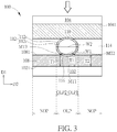
- FIG. 3 is a schematic enlargement diagram of a part of the electronic device shown in FIG 2 .
- the present disclosure introduces an electronic device 100 that includes electric elements and electrical connections between the electric elements.
- the electronic device 100 includes at least a substrate 102, and the electric elements are disposed on the substrate 102.
- the electronic device 100 may comprise liquid crystals (LC), light-emitting diodes (e.g.
- the electronic device 100 may be a display device, a flexible electronic device, a tiled electronic device, a sensing device, an antenna device, a touch electronic device, any other suitable electronic device or a combination thereof, but it is not limited.
- the substrate 102 may include a display region R1 and a peripheral region R2 disposed adjacent to the display region R1.
- the peripheral region R2 may surround the display region R1.
- At least one integrated circuit (IC) chip 104 may be disposed on the substrate 102 and in the peripheral region R2.
- a plurality of wires 122 may be disposed on the substrate 102 and extend in the display region R1 and the peripheral region R2.
- the IC chip 104 is electrically connected to the wires 122 or other electric elements (not shown) on the substrate 102.
- the electronic device 100 further comprises at least one first pad 108 disposed on the substrate 102 and at least one second pad 110 disposed opposite to the first pad 108. In FIG. 2 , two first pads 108 and two second pads 110 are shown for illustration.
- the first pads 108 are disposed on the surface 1021 of the substrate 102, wherein one or multiple layers or elements (not shown) may be disposed between or electrically connected with the first pads 108 and the substrate 102.
- one of the first pads 108 may be electrically connected to one of the wires 122 shown in FIG. 1 .
- the second pads 110 are disposed on the surface 1041 of the IC chip 104.
- one or multiple layers or elements may be disposed between the second pads 110 and the IC chip 104.
- the electronic device 100 further includes at least one conductive particle 112 disposed between the first pads 108 and the second pads 110. As shown in FIG.
- the conductive particle 112 is directly in contact with the first pad 108 and the second pad 110 such that the first pad 108 can be electrically connected to the second pad 110 through the conductive particle 112, and therefore the IC chip 104 can be electrically connected to the electric elements, such as the wire 122, through the second pad 110, the conductive particle 112 and the first pad 108.
- the second pad 110 may be a connecting pad or a bump of the IC chip 104, but not limited thereto.
- the first pad 108 has a recess 116 on its top surface 1081, and a part of the conductive particle 112 sinks in the recess 116, which means a part of the conductive particle 112 is in the recess 116, and the other part of the conductive particle 112 is positioned out of the recess 116.
- the surface of the recess 116 may be directly in contact with a surface of the lower part of the conductive particle 112, thus a contact area between the conductive particle 112 and the first pad 108 can be increased. The effect of the electrical connection between the conductive particle 112 and the first pad 108 can be improved.
- the conductive particle 112 can be fixed on the first pad 108 more firmly.
- the thickness of the first pad 108 may not be uniform, wherein the thickness of the first pad 108 indicates the total thickness from the bottom layer to the top layer of the first pad 108 in a direction D1, if the first pad 108 has multi layers. Alternatively, the total thickness indicates the distance between the bottom surface and the top surface 1081 of the first pad 108 in the direction D1.
- the direction D1 is a normal direction of the substrate 102.
- the first pad 108 has a first portion OLP that overlaps with the conductive particle 112 in the direction D1 and has a second portion NOP which does not overlap with the conductive particle 112.
- a maximum thickness T1 of the first portion OLP of the first pad 108 overlapping with the conductive particle 112 may be relatively greater than a minimum thickness T2 of the second portion NOP of the first pad 108 not overlapping with the conductive particle 112.
- the thickness T1 and the thickness T2 may be measured along the direction D1 in any cross-sectional image, so as to compare the relatively maximum or minimum value in that cross-sectional image.
- the measured thickness T1 and thickness T2 may have different values respectively, the thickness T1 is still greater than the thickness T2.
- the IC chip 101 with the second pads 110 is bonded and pressed to the substrate 102 as shown by the hollow arrow in FIG.
- the first portion OLP of the first pad 108 may be pressed to form the recess 116.
- a part of the first pad 108 may be squeezed toward the edge of the recess 116, and therefore the edge of the recess 116 may have a greater thickness, which is the thickness T1 mentioned above.
- the top surface 1081 of the first pad 108 may be relatively planar or relatively smooth before the bonding process, and the recess 116 is formed after the bonding process, but not limited thereto.
- the top surface 1081 of the first pad 108 may be relatively rough, may have recess-like structure or may have recess before the bonding process, which may help to fix the conductive particle 112 during the bonding process, but not limited thereto.
- the conductive particle 112 may include a core 112c and a shell 112s surrounding the core 112c.
- the core 112c may include resin material or other suitable material.
- the shell 112s may include conductive material, such as metal, but not limited thereto.
- the conductive particle 112 may have a round profile before the second pad 110 is bonded to the first pad 108. In the bonding process, when the second pad 110 is pressed toward the first pad 108, the conductive particle 112 positioned between the first pad 108 and the second pad 110 is also pressed to have a relatively flatter profile, such as having oval-shaped profile, and therefore the contact area between the conductive particle 112 and the first pad 108 and/or the contact area between the conductive particle 112 and the second pad 110 can be increased. After the bonding process, part of the shell 112s may be broken or have void(s) or hole(s), which may not affect the conductivity of the conductive particle 112 and the electrical connection between the first pad 108 and the second pad 110.
- FIG. 3 shows a cross-sectional schematic view of the electronic device 100, and a maximum width of the recess 116 in the direction D2 is defined as a first width W1, wherein the direction D2 is perpendicular to the direction D1.
- the first width W1 can be obtained by the following steps: defining a lowest point MT1 of the recess 116 in the first portion OLP of the first pad 108, part of the first portion OLP at one side (e.g. right side in FIG. 3 ) of the lowest point MT1 is defined as a third portion OLP1, and another part of the first portion OLP at the other side (e.g. left side in FIG.
- the lowest point MT1 is defined as a fourth portion OLP2; defining a second point MT2 in the third portion OLP1 having the thickness T1, wherein the thickness T1 is a maximum thickness of the third portion OLP1 in the direction D1; defining a third point MT3 in the fourth portion OLP2 having a thickness T3, wherein the thickness T3 is a maximum thickness of the fourth portion OLP2 in the direction D1; and measuring a distance along the direction D2 between a projection of the second point MT2 and a projection of the third point MT3 on the substrate 102 to obtain the first width W1.
- the first width W1 may be in a range from 1.5 micrometers ( ⁇ m) to 3.5 ⁇ m (1.5 ⁇ m ⁇ W1 ⁇ 3.5 ⁇ m).
- the first width W1 may be 1.7 ⁇ m, 2 ⁇ m, 2.3 ⁇ m, 2.5 ⁇ m, 2.7 ⁇ m, 3 ⁇ m or 3.2 ⁇ m, but not limited thereto.
- a maximum width of the conductive particle 112 is defined as a second width W2.
- the second width W2 can be obtained by measuring the core 112c together with the shell 112s along the direction D2.
- the second width W2 may be in a range from 2 ⁇ m to 6 ⁇ m (2 ⁇ m ⁇ W2 ⁇ 6 ⁇ m).
- the width W2 may be 2.5 ⁇ m, 3 ⁇ m, 3.5 ⁇ m, 4 ⁇ m, 4.5 ⁇ m, 5 ⁇ m or 5.5 ⁇ m, but not limited thereto.
- the first width W1 is less than or equal to the second width W2.
- the first width W1 and the second width W2 may be measured along the direction D2 in any cross-sectional image, so as to compare the relatively maximum or minimum value in that cross-sectional image.
- the electronic device 100 may have different values of the first width W1 and the second width W2 in different cross-sectional images, but the first width W1 and the second width W2 still have the same relative relationship: W1 ⁇ W2.
- a ratio of the first width W1 to the second width W2 may be in a range from 0.25 to 1 (0.25 ⁇ W1/W2 ⁇ 1).
- the ratio may be 0.3, 0.4, 0.5, 0.6, 0.7, 0.8 or 0.9, but not limited thereto.
- the above-mentioned relationships may express that the size (or projection area on the substrate 102) of the recess 116 is less than or equal to the size (or projection area on the substrate 102) of the conductive particle 112, and part of the conductive particle 112 is not contained or sink in the recess 116. This design may bring a better electrical connection effect between the first pad 108 and the second pad 110.
- the recess 116 is greater than the conductive particle 112 and most of or all of the conductive particle 112 may be sink in the recess 116.
- the contact area between the conductive particle 112 and the second pad 110 may be decreased, and the electrical connection effect between the first pad 108 and the second pad 110 may be affected.
- the recess 116 is too large, the conductive particle 112 may easily slip or roll in the recess 116, thus the difficulty of fixing the conductive particle 112 may be increased.
- the electronic device 100 may further include an adhesive layer 114 disposed between the substrate 102 and the IC chip 104, and a plurality of conductive particles 112' are disposed in the adhesive layer 114 between the substrate 102 and the IC chip 104.
- the adhesive layer 114 may also be disposed between the first pads 108 and the second pads 110, and a plurality of conductive particles 112 are disposed in the adhesive layer 114 between the first pads 108 and the second pads 110.
- an anisotropic conductive film (ACF) 115 may be provided for bonding the IC chip 104 onto the substrate 102.
- the anisotropic conductive film 115 may include the adhesive layer 114, the conductive particles 112' and the conductive particles 112.
- the conductive particles 112' may have relatively round shapes.
- the conductive particle 112 located between the first pads 108 and the second pads 110 may be pressed to have a relatively oval profile, and the conductive particle 112 may sink in the recess 116.
- the electronic device of the present disclosure is not limited to the above mentioned embodiment. Further embodiments or variant embodiments of the present disclosure are described below. It should be noted that the technical features in different embodiments described can be replaced, recombined, or mixed with one another to constitute another embodiment without departing from the spirit of the present disclosure. For making it easier to compare the difference between the embodiments and variant embodiments, the following description will detail the dissimilarities among different variant embodiments or embodiments and the identical features will not be redundantly described.
- FIG. 4 is a schematic diagram of a first pad of an electronic device according to a second embodiment of the present disclosure.
- FIG. 4 shows the profile of the first pad 108 when the anisotropic conductive film 115 and the second pad 110 have not been disposed on the first pad 108.
- the first pad 108 may be in a multilayer structure in some embodiments.
- the first pad 108 may include a first conductive set CS1 which includes multiple conductive layers, such as multiple metal layers.
- the first conductive set CS1 may include a first conductive layer 108a, a second conductive layer 108b, and a third conductive layer 108c stacked in sequence on the substrate 102 to from a stacking structure.
- a material of the first conductive layer 108a, the second conductive layer 108b, and the third conductive layer 108c may include the same or different materials.
- the first conductive set CS1 may include a stacking structure having a molybdenum (Mo) layer, an aluminum (Al) layer and a Mo layer (represented as Mo/Al/Mo stacking structure), a titanium (Ti)/Al/Ti stacking structure, a Mo/Al/Ti stacking structure, a Ti/Al/Mo stacking structure, other stacking structure with suitable materials or a combination thereof, but it is not limited thereto.
- the first conductive layer 108a is a Mo layer
- the second conductive layer 108b is an Al layer
- the third conductive layer 108c is a Mo layer.
- the second conductive layer 108b including the material of Al can have a good conductivity
- the first conductive layer 108a and the third conductive layer 108c including the material of Mo can provide better adhesion for the first pad 108 or other layers.
- the other stacking structure mentioned above may have similar structures and functions, which will not be described repeatedly.
- the first pad 108 may include at least one metal layer and a conductive protection layer CPL disposed on the at least one metal layer.
- the at least one metal layer may be a Mo layer or a Ti layer that replaces the stacking structure of the first conductive set CS1 mentioned-above or shown in FIG. 4 ; alternatively, the at least one metal layer may indicates one of the first conductive layer 108a, the second conductive layer 108b, and the third conductive layer 108c in the first conductive set CS1, but not limited thereto.
- the conductive protection layer CPL may include the conductive material with corrosion resistivity or rigidity better than metal.
- the conductive protection layer CPL may be an oxygen-containing conductive layer or an oxide layer, such as an indium tin oxide (ITO) layer, but not limited thereto.
- the electronic device 100 may further include an insulating layer 118 disposed between the first pad 108 and the substrate 102, and the first pad 108 may be directly in contact with the insulating layer 118 (e.g. the top surface of the insulating layer 118).
- the insulating layer 118 may provide buffer function during the bonding process.
- FIG. 5 is a schematic diagram of a first pad of an electronic device according to a third embodiment of the present disclosure.
- FIG. 5 shows the profile of the first pad 108 when the anisotropic conductive film 115 and the second pad 110 have not been disposed on the first pad 108.
- the first pad 108 may have an uneven top surface 1081.
- the top surface 1081 of the first pad 108 may have a certain roughness or micro-patterns before bonding. This design may help fixing the conductive particles disposed thereon.
- the top surface 1081 may also be the top surface of the third conductive layer 108c, but not limited thereto.
- the insulating layer 118 disposed between the first pad 108 and the substrate 102 may be in a multilayer structure and have a plurality of sub-insulating layers 118a, 118b, and 118c for example.
- at least one of the sub-insulating layers 118a, 118b, and 118c may have a different thickness from another one of the sub-insulating layers 118a, 118b, and 118c.
- one of the sub-insulating layers 118a, 118b, and 118c may have inconstant thickness.
- a portion of the sub-insulating layer 118b may have a thickness t1 and another portion of the sub-insulating layer 118b may have a thickness t2, the thickness t2 may be less than the thickness t1.
- the thickness t1 may correspond to the first pad 108, but not limited thereto.
- the thicker portion of the sub-insulating layer 118b may provide a buffer function during the bonding process.
- the process pressure, the process temperature, the material of the conductive particle, the thickness and property of material of the first pad, the thicknesses of the composition structure, materials of the composition layers of the first pad, and/or the roughness of the first pad can be selected and adjusted based on practical requirement by referring to all the embodiments and variant embodiments introduced in this specification.
- the materials and thicknesses of the different conductive layers of the multilayer structure of the first pad may be adjusted to obtain an expected property of the recess of the first pad.
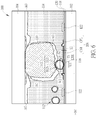
- FIG. 6 is a partial schematic outline of a scanning electron microscope (SEM) diagram of an electronic device according to a first exemplary embodiment of the present disclosure.
- one conductive particle 112 is disposed between the first pad 108 and the second pad 110.
- the first pad 108 has a first conductive set CS1 and a conductive protection layer CPL disposed on the first conductive set CS1.
- the first conductive set CS1 may include a Ti/Al/Ti stacking structure, and the conductive protection layer CPL may be an ITO layer.
- the recess 116 of the first pad 108 is formed by the conductive protection layer CPL and part of the first conductive set CS1.
- the maximum thickness T1 of the first pad 108 overlapping with the conductive particle 112 is greater than the minimum thickness T2 of the first pad 108 not overlapping with the conductive particle 112.
- the first width W1 of the recess 116 in the direction D2 is less than or equal to the second width W2 of the conductive particle 112 in the direction D2.
- the insulating layer 120 has an opening 1201 exposing the first conductive set CS1, which means at least part of a top surface of the first conductive set CS1 is exposed in the opening 1201.
- the conductive protection layer CPL covers the first conductive set CS1 in the opening 1201 and extends over the opening 1201 to cover a portion of the insulating layer 120. Accordingly, the conductive protection layer CPL is directly in contact with the first conductive set CS1 through the opening 1201, and electrically connected to the first conductive set CS1.
- the electronic device 100 may include at least one wire 122 disposed on the substrate 102 and covered by the insulating layer 120.
- FIG. 7 is a partial schematic outline of a SEM diagram of an electronic device according to a second exemplary embodiment of the present disclosure. An enlargement schematic outline of the SEM diagram is shown.
- the shell 112s of the conductive particle 112 may have irregular and uneven surface, and the second width W2 is defined by the maximum width of the outer edge of the shell 112s in the direction D2.
- the thickness T1, the thickness T3, and the first width W1 can be measured in any SEM diagram and calculated using the similar definition as mentioned in FIG. 3 , and will not be described repeatedly.
- the air gap AG may be formed by peeling resulting from cutting process of SEM sample.
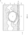
- FIG. 8 is a partial schematic outline of a SEM diagram of an electronic device according to a third exemplary embodiment of the present disclosure.
- the shell 112s of the conductive particle 112 may have one or more opening 1121, it can still provide conductivity to the first pad 108 and the second pad 110.
- the second width W2 can be obtained from the outer edge/surface of the shell 112s in the direction D2.
- FIG. 9 is a partial schematic outline of a SEM diagram of an electronic device according to a fourth exemplary embodiment of the present disclosure.
- the shell 112s has an opening 1121 and a part of the shell 112s may peel from the core 112c.
- the second width W2 may be measured from an outer edge of the core 112c to another outer edge of the core 112c or the shell 112s in the direction D2 to obtain the maximum width.
- FIG. 10 is a partial schematic outline of a SEM diagram of an electronic device according to a fifth exemplary embodiment of the present disclosure.
- the shell 112s of the conductive particle 112 may have a relatively smoother surface.
- the second width W2 of the conductive particle 112 may be measured from the outmost surface of the conductive particle 112 in the direction D2, even though the shell 112s has a protrusion P.
- An insulating layer 118 is shown between the substrate 102 and the first pad 108.
- the insulating layer 118 may be a single-layer structure or a multi-layer structure, but it is not limited thereto.
- FIG. 11 is a partial schematic outline of an optical microscope (OM) diagram of an electronic device according to a sixth exemplary embodiment of the present disclosure
- FIG. 12 is a partial schematic outline of a SEM diagram of the electronic device according to the sixth exemplary embodiment of the present disclosure, wherein FIG. 11 shows the profile of the first pad 108 when the conductive particles 112 and the second pad 110 are not disposed on the first pad 108.
- FIG. 12 two conductive particles 112 are disposed between the first pad 108 and the second pad 110.
- the first pad 108 includes a first conductive set CS1, a second conductive set CS2 disposed on the first conductive set CS1, and a conductive protection layer CPL disposed on the second conductive set CS2.
- the first conductive set CS1 and the second conductive set CS2 may independently include a Mo layer, a Ti layer, a Mo/Al/Mo structure, a Ti/Al/Ti structure, a Mo/Al/Ti structure, or a Ti/Al/Mo structure, but not limited thereto.
- both the first conductive set CS1 and the second conductive set CS2 have a Mo/Al/Mo structure.
- the conductive protection layer CPL may include an ITO layer.
- the electronic device 100 includes an insulating layer 120 covers a portion of the first conductive set CS1.
- the insulating layer 120 has an opening OP1 that exposes a portion of the first conductive set CS1.
- At least a portion of the second conductive set CS2 is disposed in the opening OP1 and directly in contact with the first conductive set CS1 through the opening OP1.
- the first conductive set CS1 is electrically connected with the second conductive set CS2 through the opening OP1.
- the electronic device 100 may further include an insulating layer 124 covers the insulating layer 120 and a portion of the second conductive set CS2.
- the insulating layer 124 has an opening OP2 that exposes a portion of the second conductive set CS2.
- the conductive protection layer CPL covers a portion of the insulating layer 124 and is directly in contact with the second conductive set CS2 through the opening OP2.
- the wires 122 disposed adjacent to the first pad 108 may have similar structures with the first conductive set CS1.
- the wires 122 may have a Mo/Al/Mo structure respectively, but not limited thereto.
- the insulating layer 120 covers the wires 122 in this exemplary embodiment.
- FIG. 13 is a partial schematic outline of a SEM diagram of an electronic device according to a seventh exemplary embodiment of the present disclosure.
- the first conductive set CS1 may include one single conductive layer, such as a Mo layer.
- the second conductive set CS2 may have a multilayer structure, such as a Mo/Al/Mo structure.
- the conductive protection layer CPL covers the second conductive set CS2 and a portion of the insulating layer 124.
- the conductive protection layer CPL may include an ITO layer, but not limited thereto.
- An insulating layer 118 is disposed between the first pad 108 and the substrate 102.
- the insulating layer 118 may serve as a buffer layer and may include silicon nitride (SiNx) or silicon oxide (SiOx) material, but not limited thereto.
- FIG. 14 is a partial schematic outline of a 3D OM diagram of an electronic device according to an eighth exemplary embodiment of the present disclosure
- FIG. 15 is a schematic profile chart obtained from the 3D OM (or OM) diagram in FIG. 14 along the line OML, wherein the FIG. 14 shows three first pads 108A, 108B, 108C and three wires 122 alternately positioned on the substrate 102.
- a plurality of recesses 116 may be shown on the surface of the first pads 108A, 108B, and/or 108C.
- recess "A”, recess "B”, recess “C”, recess “D”, recess “E”, and recess “F” are selected to calculate the vertical profiles along the line OML, so as to obtain FIG. 15 .
- the maximum thickness T1 and the secondary maximum thickness T3 can be determined according to a selected base line BAL.
- the selected base line BAL may be any horizontal line below all the measured recesses as shown in FIG. 15 .
- the first width W1 can be measured in the direction D2 between the point of the recess "B” with the maximum thickness T1 and the point of the recess “B” with the secondary maximum thickness T3, the maximum thickness T1 and the secondary maximum thickness T3 are at opposite sides of the lowest point of the recess "B".
- the depth Dp of the recess "B” can be further determined from the bottom (the point of the recess "B” with the minimum thickness determined according to the selected base line BAL) to the top (the point of the recess "B” with the maximum thickness T1) in the direction D1.
- the first width W1 and the depth Dp can be measured in different samples as the following table.
- the first width W1 of the recess may be in a range from 1.5 ⁇ m to 3.5 ⁇ m (1.5 ⁇ m ⁇ W1 ⁇ 3.5 ⁇ m), and the depth Dp of the recess may be in a range from 0.1 ⁇ m to 2.2 ⁇ m (0.1 ⁇ m ⁇ Dp ⁇ 2.2 ⁇ m), but not limited thereto.
- the first width W1 may be 1.7 ⁇ m, 2 ⁇ m, 2.3 ⁇ m, 2.5 ⁇ m, 2.7 ⁇ m, 3 ⁇ m or 3.2 ⁇ m, but not limited thereto.
- the depth Dp may be 0.3 ⁇ m, 0.5 ⁇ m, 0.7 ⁇ m, 0.9 ⁇ m, 1.1 ⁇ m, 1.3 ⁇ m, 1.5 ⁇ m, 1.7 ⁇ m or 1.9 ⁇ m, but not limited thereto.
- a third width W3 of different samples can be measured by an optical microscope (OM) before the second pad and the IC chip are removed. More specifically, the third width W3 is an average of a maximum width of any three conductive particles 112' (not the conductive particles 112) measured in any OM image.
- the third width W3 of the conductive particles 112' may be in a range from 2 ⁇ m to 6 ⁇ m (2 ⁇ m ⁇ W3 ⁇ 6 ⁇ m), but not limited thereto. In some embodiments, the third width W3 of the conductive particles 112' may be 2.5 ⁇ m, 3 ⁇ m, 3.5 ⁇ m, 4 ⁇ m, 4.5 ⁇ m, 5 ⁇ m or 5.5 ⁇ m, but not limited thereto.
- a ratio of the first width W1 to the third width W3 may be in a range from 0.25 to 1 (0.25 ⁇ W1/W3 ⁇ 1). For example, the ratio may be 0.3, 0.4, 0.5, 0.6, 0.7, 0.8 or 0.9, but not limited thereto.
- a ratio of the depth Dp to the third width W3 may be in a range from 0.01 to 0.4 (0.01 ⁇ D/W3 ⁇ 0.4).
- the ratio may be 0.05, 0.1, 0.15, 0.2, 0.25, 0.3 or 0.35, but not limited thereto.
- the third width W3 is different from the first width W1.
- the electronic device 100 of the present disclosure may include a substrate 102, a first pad (e.g. 108A) disposed on the substrate 102, and a conductive particle (e.g. the conductive particle 112' shown in FIG. 2 ) disposed on the substrate 102.
- the first pad 108A has a recess 116 with a first width W1 and the conductive particle (not shown) has a third width W3.
- the first width W1 may be in a range from 1.5 micrometers ( ⁇ m) to 3.5 ⁇ m (1.5 ⁇ m ⁇ W1 ⁇ 3.5 ⁇ m).
- the first width W1 may be 1.7 ⁇ m, 2 ⁇ m, 2.3 ⁇ m, 2.5 ⁇ m, 2.7 ⁇ m, 3 ⁇ m or 3.2 ⁇ m, but not limited thereto.
- the third width W3 may be in a range from 2 ⁇ m to 6 ⁇ m (2 ⁇ m ⁇ W2 ⁇ 6 ⁇ m).
- the third width W3 may be 2.5 ⁇ m, 3 ⁇ m, 3.5 ⁇ m, 4 ⁇ m, 4.5 ⁇ m, 5 ⁇ m or 5.5 ⁇ m, but not limited thereto.
- the first width W1 is less than or equal to the third width W3 (W1 ⁇ W3).
- the ratio of the first width W1 to the third width W3 is in a range from 0.25 to 1 (0.25 ⁇ W1/W3 ⁇ 1).
- the ratio may be 0.3, 0.4, 0.5, 0.6, 0.7, 0.8 or 0.9, but not limited thereto.
- the roughness Ra and the roughness Rms of the first pads 108A, 108B, 108C can be measured by 3D OM. As shown in Fig. 14 , a constant area represent by the frame ARL can be selected for measuring the first pads 108A, 108B, 108C to obtain the roughness Ra and/or Rms. In some embodiments, the roughness may be in a range from 0.01 ⁇ m to 0.3 ⁇ m (0.01 ⁇ m ⁇ roughness ⁇ 0.3 ⁇ m), but not limited thereto.
- the roughness Ra may be in a range from 0.01 ⁇ m to 0.2 ⁇ m (0.01 ⁇ m ⁇ Ra ⁇ 0.2 ⁇ m), and the roughness Rms may be in a range from 0.02 ⁇ m to 0.3 ⁇ m (0.02 ⁇ m ⁇ Rms ⁇ 0.3 ⁇ m), but not limited thereto.
- the roughness Ra may be 0.05 ⁇ m, 0.07 ⁇ m, 0.1 ⁇ m, 0.13 ⁇ m, 0.15 ⁇ m or 0.17 ⁇ m, but not limited thereto.
- the roughness Rms may be 0.05 ⁇ m, 0.07 ⁇ m, 0.1 ⁇ m, 0.13 ⁇ m, 0.15 ⁇ m, 0.17 ⁇ m, 0.2 ⁇ m, 0.23 ⁇ m, 0.25 ⁇ m or 0.27 ⁇ m, but not limited thereto.
- the roughness Ra may be in a range from 0.020 ⁇ m to 0.043 ⁇ m (0.020 ⁇ m ⁇ Ra ⁇ 0.043 ⁇ m), and the roughness Rms may be in a range from 0.033 ⁇ m to 0.079 ⁇ m (0.033 ⁇ m ⁇ Rms ⁇ 0.079 ⁇ m), but not limited thereto.
- the roughness Rm and Rms may be measured by atomic force microscope (AFM), 3D OM or any other suitable instruments.
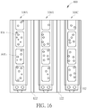
- FIG. 16 is a partial schematic outline of a 3D OM (or OM) diagram of an electronic device according to a ninth exemplary embodiment of the present disclosure.
- This exemplary embodiment shows another kind of first pads 108A, 108B, 108C with different outline.
- the roughness Rm and Rms can be obtained, wherein the area represented by the frame ARL is determined to measure the roughness.
- the roughness Ra may be in a range from 0.05 ⁇ m to 0.15 ⁇ m (0.05 ⁇ m ⁇ Ra ⁇ 0.15 ⁇ m), and the roughness Rms may be in a range from 0.1 ⁇ m to 0.2 ⁇ m (0.1 ⁇ m ⁇ Rms ⁇ 0.2 ⁇ m), but not limited thereto.
- the roughness Ra may be 0.06 ⁇ m, 0.07 ⁇ m, 0.08 ⁇ m, 0.09 ⁇ m, 0.1 ⁇ m, 0.11 ⁇ m, 0.12 ⁇ m, 0.13 ⁇ m or 0.14 ⁇ m, but not limited thereto.
- the roughness Rms may be 0.11 ⁇ m, 0.12 ⁇ m, 0.13 ⁇ m, 0.14 ⁇ m, 0.15 ⁇ m, 0.16 ⁇ m, 0.17 ⁇ m, 0.18 ⁇ m or 0.19 ⁇ m, but not limited thereto.
- a conductive particle may be used for electrically connecting a first pad and a second pad in an electronic device.
- the first pad may have a recess corresponding to the conductive particle.
- the conductive particle may sink in the recess, the contact area between the first pad and the conductive particle may be increased, and the electrical connection between the first pad and the conductive particle may be improved.
- the recess may help fixing the conductive particle more firmly for bonding or electrical connection between the first pad and the second pad.
- Different structures and/or compositions of the conductive layers of the first pad may be provided based on different requirements. For example, oxygen-containing conductive material or oxide conductive material may be adopted to form the top surface of the first pad.
Landscapes
- Internal Circuitry In Semiconductor Integrated Circuit Devices (AREA)
- Wire Bonding (AREA)
Applications Claiming Priority (1)
| Application Number | Priority Date | Filing Date | Title |
|---|---|---|---|
| US16/412,375 US11217557B2 (en) | 2019-05-14 | 2019-05-14 | Electronic device having conductive particle between pads |
Publications (2)
| Publication Number | Publication Date |
|---|---|
| EP3748673A2 true EP3748673A2 (de) | 2020-12-09 |
| EP3748673A3 EP3748673A3 (de) | 2021-04-07 |
Family
ID=70292793
Family Applications (1)
| Application Number | Title | Priority Date | Filing Date |
|---|---|---|---|
| EP20169739.8A Withdrawn EP3748673A3 (de) | 2019-05-14 | 2020-04-16 | Elektronische vorrichtung mit einer eine erste anschlussfläche mit einer zweiten anschlussfläche verbindenden und in einer vertiefung in der ersten anschlussfläche sinkenden leitenden partikel |
Country Status (4)
| Country | Link |
|---|---|
| US (3) | US11217557B2 (de) |
| EP (1) | EP3748673A3 (de) |
| CN (2) | CN116779583A (de) |
| PH (1) | PH12020050123A1 (de) |
Families Citing this family (1)
| Publication number | Priority date | Publication date | Assignee | Title |
|---|---|---|---|---|
| CN116960129A (zh) * | 2022-04-13 | 2023-10-27 | 群创光电股份有限公司 | 电子装置 |
Family Cites Families (22)
| Publication number | Priority date | Publication date | Assignee | Title |
|---|---|---|---|---|
| JP3284262B2 (ja) | 1996-09-05 | 2002-05-20 | セイコーエプソン株式会社 | 液晶表示装置及びそれを用いた電子機器 |
| KR100737896B1 (ko) | 2001-02-07 | 2007-07-10 | 삼성전자주식회사 | 어레이 기판과, 액정표시장치 및 그 제조방법 |
| US7038327B2 (en) * | 2003-11-11 | 2006-05-02 | Au Optronics Corp. | Anisotropic conductive film bonding pad |
| JP2006309028A (ja) * | 2005-04-28 | 2006-11-09 | Sanyo Epson Imaging Devices Corp | 表示装置および表示装置の製造方法 |
| JP2008192984A (ja) * | 2007-02-07 | 2008-08-21 | Elpida Memory Inc | 半導体装置及びその製造方法 |
| JP2008203484A (ja) | 2007-02-20 | 2008-09-04 | Epson Imaging Devices Corp | 電気光学装置、フレキシブル回路基板の実装構造体及び電子機器 |
| CN105778815B (zh) * | 2007-10-31 | 2018-03-20 | 日立化成株式会社 | 电路部件的连接结构和电路部件的连接方法 |
| US8796691B2 (en) | 2008-09-18 | 2014-08-05 | Innolux Corporation | System for displaying images and fabricating method thereof |
| TWI395279B (zh) * | 2009-12-30 | 2013-05-01 | 財團法人工業技術研究院 | 微凸塊結構 |
| JP5303489B2 (ja) * | 2010-02-16 | 2013-10-02 | ルネサスエレクトロニクス株式会社 | 半導体装置の製造方法 |
| TWI446314B (zh) * | 2010-08-19 | 2014-07-21 | 友達光電股份有限公司 | 畫素陣列基板、導電結構以及顯示面板 |
| US8729699B2 (en) * | 2011-10-18 | 2014-05-20 | Taiwan Semiconductor Manufacturing Company, Ltd. | Connector structures of integrated circuits |
| US8922006B2 (en) * | 2012-03-29 | 2014-12-30 | Taiwan Semiconductor Manufacturing Company, Ltd. | Elongated bumps in integrated circuit devices |
| US9437551B2 (en) * | 2014-02-13 | 2016-09-06 | Taiwan Semiconductor Manufacturing Company, Ltd. | Concentric bump design for the alignment in die stacking |
| JP2015179831A (ja) * | 2014-02-27 | 2015-10-08 | デクセリアルズ株式会社 | 接続体、接続体の製造方法及び検査方法 |
| US9507222B2 (en) * | 2014-03-14 | 2016-11-29 | Innolux Corporation | Display device |
| TWI546850B (zh) | 2014-11-14 | 2016-08-21 | 群創光電股份有限公司 | 顯示面板之製備方法 |
| US10069041B2 (en) | 2016-08-05 | 2018-09-04 | Innolux Corporation | Display apparatus and manufacturing method thereof |
| US10191345B2 (en) | 2016-11-01 | 2019-01-29 | Innolux Corporation | Display device |
| JP6967371B2 (ja) | 2017-05-26 | 2021-11-17 | 株式会社ジャパンディスプレイ | アクティブマトリクス基板 |
| CN109686719B (zh) | 2017-10-18 | 2021-09-21 | 群创光电股份有限公司 | 电子装置及包含其的显示设备 |
| KR102519126B1 (ko) * | 2018-03-30 | 2023-04-06 | 삼성디스플레이 주식회사 | 표시 장치 |
-
2019
- 2019-05-14 US US16/412,375 patent/US11217557B2/en active Active
-
2020
- 2020-04-16 EP EP20169739.8A patent/EP3748673A3/de not_active Withdrawn
- 2020-04-17 CN CN202310751266.9A patent/CN116779583A/zh active Pending
- 2020-04-17 CN CN202010304553.1A patent/CN111952278B/zh active Active
- 2020-05-04 PH PH12020050123A patent/PH12020050123A1/en unknown
-
2021
- 2021-11-23 US US17/534,414 patent/US12062637B2/en active Active
-
2024
- 2024-07-08 US US18/765,370 patent/US20240363582A1/en active Pending
Also Published As
| Publication number | Publication date |
|---|---|
| US20200365551A1 (en) | 2020-11-19 |
| PH12020050123A1 (en) | 2021-11-22 |
| US20240363582A1 (en) | 2024-10-31 |
| US20220084982A1 (en) | 2022-03-17 |
| CN111952278B (zh) | 2023-07-14 |
| US12062637B2 (en) | 2024-08-13 |
| CN116779583A (zh) | 2023-09-19 |
| CN111952278A (zh) | 2020-11-17 |
| EP3748673A3 (de) | 2021-04-07 |
| US11217557B2 (en) | 2022-01-04 |
Similar Documents
| Publication | Publication Date | Title |
|---|---|---|
| TW484194B (en) | Semiconductor device and method of manufacturing the same | |
| KR101051908B1 (ko) | 금속 베이스 회로 기판과 그 제조 방법 | |
| TWI761171B (zh) | 面板裝置及面板裝置的製造方法 | |
| GB2303523A (en) | Solderless tag device with integral capacitance between IC and antenna terminals | |
| CN113543468B (zh) | 电子装置 | |
| US10672697B2 (en) | Wiring board and electronic package | |
| US20240363582A1 (en) | Electronic device | |
| WO2019007412A1 (zh) | 一种影像传感芯片的封装结构及其封装方法 | |
| TWI356481B (en) | Bump structure | |
| CN113506810A (zh) | 面板装置及面板装置的制造方法 | |
| JP2006134912A (ja) | 半導体モジュールおよびその製造方法、ならびにフィルムインターポーザ | |
| CN112071819B (zh) | 电子装置 | |
| TWI758090B (zh) | 電子裝置及其製造方法 | |
| TWI277190B (en) | Package structure for electronic device | |
| CN112201640A (zh) | 电子装置 | |
| WO2023088438A1 (zh) | 屏幕模组、电子设备和屏幕模组的制造方法 | |
| TW202416486A (zh) | 電子裝置及其製造方法 | |
| CN117913055A (zh) | 电子装置及其制造方法 | |
| US7119423B2 (en) | Semiconductor device and method of manufacturing the same, electronic module, and electronic instrument | |
| CN101409265B (zh) | 用于一半导体封装结构的基板、半导体封装结构及其制造方法 | |
| US12456670B2 (en) | Electronic device | |
| TWI801172B (zh) | 電子裝置 | |
| US20250294677A1 (en) | Resin multilayer substrate and electronic device | |
| WO2024070439A1 (ja) | 電子素子、および電子素子の搬送体 | |
| EP3812832A1 (de) | Elektronische vorrichtung |
Legal Events
| Date | Code | Title | Description |
|---|---|---|---|
| PUAI | Public reference made under article 153(3) epc to a published international application that has entered the european phase |
Free format text: ORIGINAL CODE: 0009012 |
|
| STAA | Information on the status of an ep patent application or granted ep patent |
Free format text: STATUS: THE APPLICATION HAS BEEN PUBLISHED |
|
| AK | Designated contracting states |
Kind code of ref document: A2 Designated state(s): AL AT BE BG CH CY CZ DE DK EE ES FI FR GB GR HR HU IE IS IT LI LT LU LV MC MK MT NL NO PL PT RO RS SE SI SK SM TR |
|
| AX | Request for extension of the european patent |
Extension state: BA ME |
|
| PUAL | Search report despatched |
Free format text: ORIGINAL CODE: 0009013 |
|
| AK | Designated contracting states |
Kind code of ref document: A3 Designated state(s): AL AT BE BG CH CY CZ DE DK EE ES FI FR GB GR HR HU IE IS IT LI LT LU LV MC MK MT NL NO PL PT RO RS SE SI SK SM TR |
|
| AX | Request for extension of the european patent |
Extension state: BA ME |
|
| RIC1 | Information provided on ipc code assigned before grant |
Ipc: H01L 23/488 20060101AFI20210302BHEP Ipc: H01L 21/60 20060101ALI20210302BHEP |
|
| STAA | Information on the status of an ep patent application or granted ep patent |
Free format text: STATUS: THE APPLICATION IS DEEMED TO BE WITHDRAWN |
|
| 18D | Application deemed to be withdrawn |
Effective date: 20211008 |