EP3742481A2 - Semiconductor die with an aluminium pad coated by a sintered silver structure for a clip and with an uncoated aluminium pad for a bond wire and corresponding manufacturing method - Google Patents
Semiconductor die with an aluminium pad coated by a sintered silver structure for a clip and with an uncoated aluminium pad for a bond wire and corresponding manufacturing method Download PDFInfo
- Publication number
- EP3742481A2 EP3742481A2 EP20174492.7A EP20174492A EP3742481A2 EP 3742481 A2 EP3742481 A2 EP 3742481A2 EP 20174492 A EP20174492 A EP 20174492A EP 3742481 A2 EP3742481 A2 EP 3742481A2
- Authority
- EP
- European Patent Office
- Prior art keywords
- aluminum
- silver
- pad
- aluminum pad
- sintered
- Prior art date
- Legal status (The legal status is an assumption and is not a legal conclusion. Google has not performed a legal analysis and makes no representation as to the accuracy of the status listed.)
- Pending
Links
Images




Classifications
-
- H—ELECTRICITY
- H10—SEMICONDUCTOR DEVICES; ELECTRIC SOLID-STATE DEVICES NOT OTHERWISE PROVIDED FOR
- H10W—GENERIC PACKAGES, INTERCONNECTIONS, CONNECTORS OR OTHER CONSTRUCTIONAL DETAILS OF DEVICES COVERED BY CLASS H10
- H10W40/00—Arrangements for thermal protection or thermal control
- H10W40/20—Arrangements for cooling
- H10W40/25—Arrangements for cooling characterised by their materials
- H10W40/255—Arrangements for cooling characterised by their materials having a laminate or multilayered structure, e.g. direct bond copper [DBC] ceramic substrates
-
- H—ELECTRICITY
- H10—SEMICONDUCTOR DEVICES; ELECTRIC SOLID-STATE DEVICES NOT OTHERWISE PROVIDED FOR
- H10W—GENERIC PACKAGES, INTERCONNECTIONS, CONNECTORS OR OTHER CONSTRUCTIONAL DETAILS OF DEVICES COVERED BY CLASS H10
- H10W70/00—Package substrates; Interposers; Redistribution layers [RDL]
- H10W70/40—Leadframes
- H10W70/411—Chip-supporting parts, e.g. die pads
- H10W70/417—Bonding materials between chips and die pads
-
- H—ELECTRICITY
- H10—SEMICONDUCTOR DEVICES; ELECTRIC SOLID-STATE DEVICES NOT OTHERWISE PROVIDED FOR
- H10W—GENERIC PACKAGES, INTERCONNECTIONS, CONNECTORS OR OTHER CONSTRUCTIONAL DETAILS OF DEVICES COVERED BY CLASS H10
- H10W70/00—Package substrates; Interposers; Redistribution layers [RDL]
- H10W70/40—Leadframes
- H10W70/464—Additional interconnections in combination with leadframes
- H10W70/466—Tape carriers or flat leads
-
- H—ELECTRICITY
- H10—SEMICONDUCTOR DEVICES; ELECTRIC SOLID-STATE DEVICES NOT OTHERWISE PROVIDED FOR
- H10W—GENERIC PACKAGES, INTERCONNECTIONS, CONNECTORS OR OTHER CONSTRUCTIONAL DETAILS OF DEVICES COVERED BY CLASS H10
- H10W70/00—Package substrates; Interposers; Redistribution layers [RDL]
- H10W70/40—Leadframes
- H10W70/481—Leadframes for devices being provided for in groups H10D8/00 - H10D48/00
-
- H—ELECTRICITY
- H10—SEMICONDUCTOR DEVICES; ELECTRIC SOLID-STATE DEVICES NOT OTHERWISE PROVIDED FOR
- H10W—GENERIC PACKAGES, INTERCONNECTIONS, CONNECTORS OR OTHER CONSTRUCTIONAL DETAILS OF DEVICES COVERED BY CLASS H10
- H10W20/00—Interconnections in chips, wafers or substrates
- H10W20/40—Interconnections external to wafers or substrates, e.g. back-end-of-line [BEOL] metallisations or vias connecting to gate electrodes
-
- H—ELECTRICITY
- H10—SEMICONDUCTOR DEVICES; ELECTRIC SOLID-STATE DEVICES NOT OTHERWISE PROVIDED FOR
- H10W—GENERIC PACKAGES, INTERCONNECTIONS, CONNECTORS OR OTHER CONSTRUCTIONAL DETAILS OF DEVICES COVERED BY CLASS H10
- H10W72/00—Interconnections or connectors in packages
-
- H—ELECTRICITY
- H10—SEMICONDUCTOR DEVICES; ELECTRIC SOLID-STATE DEVICES NOT OTHERWISE PROVIDED FOR
- H10W—GENERIC PACKAGES, INTERCONNECTIONS, CONNECTORS OR OTHER CONSTRUCTIONAL DETAILS OF DEVICES COVERED BY CLASS H10
- H10W72/00—Interconnections or connectors in packages
- H10W72/01—Manufacture or treatment
- H10W72/019—Manufacture or treatment of bond pads
- H10W72/01921—Manufacture or treatment of bond pads using local deposition
- H10W72/01923—Manufacture or treatment of bond pads using local deposition in liquid form, e.g. by dispensing droplets or by screen printing
-
- H—ELECTRICITY
- H10—SEMICONDUCTOR DEVICES; ELECTRIC SOLID-STATE DEVICES NOT OTHERWISE PROVIDED FOR
- H10W—GENERIC PACKAGES, INTERCONNECTIONS, CONNECTORS OR OTHER CONSTRUCTIONAL DETAILS OF DEVICES COVERED BY CLASS H10
- H10W72/00—Interconnections or connectors in packages
- H10W72/01—Manufacture or treatment
- H10W72/019—Manufacture or treatment of bond pads
- H10W72/01931—Manufacture or treatment of bond pads using blanket deposition
- H10W72/01938—Manufacture or treatment of bond pads using blanket deposition in gaseous form, e.g. by CVD or PVD
-
- H—ELECTRICITY
- H10—SEMICONDUCTOR DEVICES; ELECTRIC SOLID-STATE DEVICES NOT OTHERWISE PROVIDED FOR
- H10W—GENERIC PACKAGES, INTERCONNECTIONS, CONNECTORS OR OTHER CONSTRUCTIONAL DETAILS OF DEVICES COVERED BY CLASS H10
- H10W72/00—Interconnections or connectors in packages
- H10W72/01—Manufacture or treatment
- H10W72/019—Manufacture or treatment of bond pads
- H10W72/01961—Chemical or physical modification, e.g. by sintering or anodisation
-
- H—ELECTRICITY
- H10—SEMICONDUCTOR DEVICES; ELECTRIC SOLID-STATE DEVICES NOT OTHERWISE PROVIDED FOR
- H10W—GENERIC PACKAGES, INTERCONNECTIONS, CONNECTORS OR OTHER CONSTRUCTIONAL DETAILS OF DEVICES COVERED BY CLASS H10
- H10W72/00—Interconnections or connectors in packages
- H10W72/01—Manufacture or treatment
- H10W72/019—Manufacture or treatment of bond pads
- H10W72/01971—Cleaning, e.g. oxide removal
-
- H—ELECTRICITY
- H10—SEMICONDUCTOR DEVICES; ELECTRIC SOLID-STATE DEVICES NOT OTHERWISE PROVIDED FOR
- H10W—GENERIC PACKAGES, INTERCONNECTIONS, CONNECTORS OR OTHER CONSTRUCTIONAL DETAILS OF DEVICES COVERED BY CLASS H10
- H10W72/00—Interconnections or connectors in packages
- H10W72/01—Manufacture or treatment
- H10W72/0198—Manufacture or treatment batch processes
-
- H—ELECTRICITY
- H10—SEMICONDUCTOR DEVICES; ELECTRIC SOLID-STATE DEVICES NOT OTHERWISE PROVIDED FOR
- H10W—GENERIC PACKAGES, INTERCONNECTIONS, CONNECTORS OR OTHER CONSTRUCTIONAL DETAILS OF DEVICES COVERED BY CLASS H10
- H10W72/00—Interconnections or connectors in packages
- H10W72/071—Connecting or disconnecting
- H10W72/073—Connecting or disconnecting of die-attach connectors
-
- H—ELECTRICITY
- H10—SEMICONDUCTOR DEVICES; ELECTRIC SOLID-STATE DEVICES NOT OTHERWISE PROVIDED FOR
- H10W—GENERIC PACKAGES, INTERCONNECTIONS, CONNECTORS OR OTHER CONSTRUCTIONAL DETAILS OF DEVICES COVERED BY CLASS H10
- H10W72/00—Interconnections or connectors in packages
- H10W72/071—Connecting or disconnecting
- H10W72/075—Connecting or disconnecting of bond wires
-
- H—ELECTRICITY
- H10—SEMICONDUCTOR DEVICES; ELECTRIC SOLID-STATE DEVICES NOT OTHERWISE PROVIDED FOR
- H10W—GENERIC PACKAGES, INTERCONNECTIONS, CONNECTORS OR OTHER CONSTRUCTIONAL DETAILS OF DEVICES COVERED BY CLASS H10
- H10W72/00—Interconnections or connectors in packages
- H10W72/071—Connecting or disconnecting
- H10W72/075—Connecting or disconnecting of bond wires
- H10W72/07521—Aligning
-
- H—ELECTRICITY
- H10—SEMICONDUCTOR DEVICES; ELECTRIC SOLID-STATE DEVICES NOT OTHERWISE PROVIDED FOR
- H10W—GENERIC PACKAGES, INTERCONNECTIONS, CONNECTORS OR OTHER CONSTRUCTIONAL DETAILS OF DEVICES COVERED BY CLASS H10
- H10W72/00—Interconnections or connectors in packages
- H10W72/071—Connecting or disconnecting
- H10W72/075—Connecting or disconnecting of bond wires
- H10W72/07531—Techniques
- H10W72/07532—Compression bonding, e.g. thermocompression bonding
- H10W72/07533—Ultrasonic bonding, e.g. thermosonic bonding
-
- H—ELECTRICITY
- H10—SEMICONDUCTOR DEVICES; ELECTRIC SOLID-STATE DEVICES NOT OTHERWISE PROVIDED FOR
- H10W—GENERIC PACKAGES, INTERCONNECTIONS, CONNECTORS OR OTHER CONSTRUCTIONAL DETAILS OF DEVICES COVERED BY CLASS H10
- H10W72/00—Interconnections or connectors in packages
- H10W72/071—Connecting or disconnecting
- H10W72/075—Connecting or disconnecting of bond wires
- H10W72/07551—Connecting or disconnecting of bond wires characterised by changes in properties of the bond wires during the connecting
- H10W72/07552—Connecting or disconnecting of bond wires characterised by changes in properties of the bond wires during the connecting changes in structures or sizes
-
- H—ELECTRICITY
- H10—SEMICONDUCTOR DEVICES; ELECTRIC SOLID-STATE DEVICES NOT OTHERWISE PROVIDED FOR
- H10W—GENERIC PACKAGES, INTERCONNECTIONS, CONNECTORS OR OTHER CONSTRUCTIONAL DETAILS OF DEVICES COVERED BY CLASS H10
- H10W72/00—Interconnections or connectors in packages
- H10W72/071—Connecting or disconnecting
- H10W72/076—Connecting or disconnecting of strap connectors
-
- H—ELECTRICITY
- H10—SEMICONDUCTOR DEVICES; ELECTRIC SOLID-STATE DEVICES NOT OTHERWISE PROVIDED FOR
- H10W—GENERIC PACKAGES, INTERCONNECTIONS, CONNECTORS OR OTHER CONSTRUCTIONAL DETAILS OF DEVICES COVERED BY CLASS H10
- H10W72/00—Interconnections or connectors in packages
- H10W72/071—Connecting or disconnecting
- H10W72/076—Connecting or disconnecting of strap connectors
- H10W72/07631—Techniques
-
- H—ELECTRICITY
- H10—SEMICONDUCTOR DEVICES; ELECTRIC SOLID-STATE DEVICES NOT OTHERWISE PROVIDED FOR
- H10W—GENERIC PACKAGES, INTERCONNECTIONS, CONNECTORS OR OTHER CONSTRUCTIONAL DETAILS OF DEVICES COVERED BY CLASS H10
- H10W72/00—Interconnections or connectors in packages
- H10W72/071—Connecting or disconnecting
- H10W72/076—Connecting or disconnecting of strap connectors
- H10W72/07631—Techniques
- H10W72/07632—Compression bonding, e.g. thermocompression bonding
- H10W72/07633—Ultrasonic bonding, e.g. thermosonic bonding
-
- H—ELECTRICITY
- H10—SEMICONDUCTOR DEVICES; ELECTRIC SOLID-STATE DEVICES NOT OTHERWISE PROVIDED FOR
- H10W—GENERIC PACKAGES, INTERCONNECTIONS, CONNECTORS OR OTHER CONSTRUCTIONAL DETAILS OF DEVICES COVERED BY CLASS H10
- H10W72/00—Interconnections or connectors in packages
- H10W72/071—Connecting or disconnecting
- H10W72/076—Connecting or disconnecting of strap connectors
- H10W72/07631—Techniques
- H10W72/07636—Soldering or alloying
-
- H—ELECTRICITY
- H10—SEMICONDUCTOR DEVICES; ELECTRIC SOLID-STATE DEVICES NOT OTHERWISE PROVIDED FOR
- H10W—GENERIC PACKAGES, INTERCONNECTIONS, CONNECTORS OR OTHER CONSTRUCTIONAL DETAILS OF DEVICES COVERED BY CLASS H10
- H10W72/00—Interconnections or connectors in packages
- H10W72/071—Connecting or disconnecting
- H10W72/076—Connecting or disconnecting of strap connectors
- H10W72/07651—Connecting or disconnecting of strap connectors characterised by changes in properties of the strap connectors during connecting
- H10W72/07653—Connecting or disconnecting of strap connectors characterised by changes in properties of the strap connectors during connecting changes in shapes
-
- H—ELECTRICITY
- H10—SEMICONDUCTOR DEVICES; ELECTRIC SOLID-STATE DEVICES NOT OTHERWISE PROVIDED FOR
- H10W—GENERIC PACKAGES, INTERCONNECTIONS, CONNECTORS OR OTHER CONSTRUCTIONAL DETAILS OF DEVICES COVERED BY CLASS H10
- H10W72/00—Interconnections or connectors in packages
- H10W72/50—Bond wires
- H10W72/521—Structures or relative sizes of bond wires
- H10W72/527—Multiple bond wires having different sizes
-
- H—ELECTRICITY
- H10—SEMICONDUCTOR DEVICES; ELECTRIC SOLID-STATE DEVICES NOT OTHERWISE PROVIDED FOR
- H10W—GENERIC PACKAGES, INTERCONNECTIONS, CONNECTORS OR OTHER CONSTRUCTIONAL DETAILS OF DEVICES COVERED BY CLASS H10
- H10W72/00—Interconnections or connectors in packages
- H10W72/50—Bond wires
- H10W72/531—Shapes of wire connectors
- H10W72/533—Cross-sectional shape
- H10W72/534—Cross-sectional shape being rectangular
-
- H—ELECTRICITY
- H10—SEMICONDUCTOR DEVICES; ELECTRIC SOLID-STATE DEVICES NOT OTHERWISE PROVIDED FOR
- H10W—GENERIC PACKAGES, INTERCONNECTIONS, CONNECTORS OR OTHER CONSTRUCTIONAL DETAILS OF DEVICES COVERED BY CLASS H10
- H10W72/00—Interconnections or connectors in packages
- H10W72/50—Bond wires
- H10W72/531—Shapes of wire connectors
- H10W72/536—Shapes of wire connectors the connected ends being ball-shaped
-
- H—ELECTRICITY
- H10—SEMICONDUCTOR DEVICES; ELECTRIC SOLID-STATE DEVICES NOT OTHERWISE PROVIDED FOR
- H10W—GENERIC PACKAGES, INTERCONNECTIONS, CONNECTORS OR OTHER CONSTRUCTIONAL DETAILS OF DEVICES COVERED BY CLASS H10
- H10W72/00—Interconnections or connectors in packages
- H10W72/50—Bond wires
- H10W72/531—Shapes of wire connectors
- H10W72/5363—Shapes of wire connectors the connected ends being wedge-shaped
-
- H—ELECTRICITY
- H10—SEMICONDUCTOR DEVICES; ELECTRIC SOLID-STATE DEVICES NOT OTHERWISE PROVIDED FOR
- H10W—GENERIC PACKAGES, INTERCONNECTIONS, CONNECTORS OR OTHER CONSTRUCTIONAL DETAILS OF DEVICES COVERED BY CLASS H10
- H10W72/00—Interconnections or connectors in packages
- H10W72/50—Bond wires
- H10W72/541—Dispositions of bond wires
- H10W72/547—Dispositions of multiple bond wires
- H10W72/5473—Dispositions of multiple bond wires multiple bond wires connected to a common bond pad
-
- H—ELECTRICITY
- H10—SEMICONDUCTOR DEVICES; ELECTRIC SOLID-STATE DEVICES NOT OTHERWISE PROVIDED FOR
- H10W—GENERIC PACKAGES, INTERCONNECTIONS, CONNECTORS OR OTHER CONSTRUCTIONAL DETAILS OF DEVICES COVERED BY CLASS H10
- H10W72/00—Interconnections or connectors in packages
- H10W72/50—Bond wires
- H10W72/551—Materials of bond wires
-
- H—ELECTRICITY
- H10—SEMICONDUCTOR DEVICES; ELECTRIC SOLID-STATE DEVICES NOT OTHERWISE PROVIDED FOR
- H10W—GENERIC PACKAGES, INTERCONNECTIONS, CONNECTORS OR OTHER CONSTRUCTIONAL DETAILS OF DEVICES COVERED BY CLASS H10
- H10W72/00—Interconnections or connectors in packages
- H10W72/50—Bond wires
- H10W72/59—Bond pads specially adapted therefor
-
- H—ELECTRICITY
- H10—SEMICONDUCTOR DEVICES; ELECTRIC SOLID-STATE DEVICES NOT OTHERWISE PROVIDED FOR
- H10W—GENERIC PACKAGES, INTERCONNECTIONS, CONNECTORS OR OTHER CONSTRUCTIONAL DETAILS OF DEVICES COVERED BY CLASS H10
- H10W72/00—Interconnections or connectors in packages
- H10W72/60—Strap connectors, e.g. thick copper clips for grounding of power devices
- H10W72/631—Shapes of strap connectors
-
- H—ELECTRICITY
- H10—SEMICONDUCTOR DEVICES; ELECTRIC SOLID-STATE DEVICES NOT OTHERWISE PROVIDED FOR
- H10W—GENERIC PACKAGES, INTERCONNECTIONS, CONNECTORS OR OTHER CONSTRUCTIONAL DETAILS OF DEVICES COVERED BY CLASS H10
- H10W72/00—Interconnections or connectors in packages
- H10W72/60—Strap connectors, e.g. thick copper clips for grounding of power devices
- H10W72/641—Dispositions of strap connectors
- H10W72/646—Dispositions of strap connectors the connected ends being on auxiliary connecting means on bond pads, e.g. on a bump connector
-
- H—ELECTRICITY
- H10—SEMICONDUCTOR DEVICES; ELECTRIC SOLID-STATE DEVICES NOT OTHERWISE PROVIDED FOR
- H10W—GENERIC PACKAGES, INTERCONNECTIONS, CONNECTORS OR OTHER CONSTRUCTIONAL DETAILS OF DEVICES COVERED BY CLASS H10
- H10W72/00—Interconnections or connectors in packages
- H10W72/60—Strap connectors, e.g. thick copper clips for grounding of power devices
- H10W72/691—Bond pads specially adapted therefor
-
- H—ELECTRICITY
- H10—SEMICONDUCTOR DEVICES; ELECTRIC SOLID-STATE DEVICES NOT OTHERWISE PROVIDED FOR
- H10W—GENERIC PACKAGES, INTERCONNECTIONS, CONNECTORS OR OTHER CONSTRUCTIONAL DETAILS OF DEVICES COVERED BY CLASS H10
- H10W72/00—Interconnections or connectors in packages
- H10W72/851—Dispositions of multiple connectors or interconnections
- H10W72/853—On the same surface
- H10W72/871—Bond wires and strap connectors
-
- H—ELECTRICITY
- H10—SEMICONDUCTOR DEVICES; ELECTRIC SOLID-STATE DEVICES NOT OTHERWISE PROVIDED FOR
- H10W—GENERIC PACKAGES, INTERCONNECTIONS, CONNECTORS OR OTHER CONSTRUCTIONAL DETAILS OF DEVICES COVERED BY CLASS H10
- H10W72/00—Interconnections or connectors in packages
- H10W72/851—Dispositions of multiple connectors or interconnections
- H10W72/874—On different surfaces
-
- H—ELECTRICITY
- H10—SEMICONDUCTOR DEVICES; ELECTRIC SOLID-STATE DEVICES NOT OTHERWISE PROVIDED FOR
- H10W—GENERIC PACKAGES, INTERCONNECTIONS, CONNECTORS OR OTHER CONSTRUCTIONAL DETAILS OF DEVICES COVERED BY CLASS H10
- H10W72/00—Interconnections or connectors in packages
- H10W72/851—Dispositions of multiple connectors or interconnections
- H10W72/874—On different surfaces
- H10W72/884—Die-attach connectors and bond wires
-
- H—ELECTRICITY
- H10—SEMICONDUCTOR DEVICES; ELECTRIC SOLID-STATE DEVICES NOT OTHERWISE PROVIDED FOR
- H10W—GENERIC PACKAGES, INTERCONNECTIONS, CONNECTORS OR OTHER CONSTRUCTIONAL DETAILS OF DEVICES COVERED BY CLASS H10
- H10W72/00—Interconnections or connectors in packages
- H10W72/851—Dispositions of multiple connectors or interconnections
- H10W72/874—On different surfaces
- H10W72/886—Die-attach connectors and strap connectors
-
- H—ELECTRICITY
- H10—SEMICONDUCTOR DEVICES; ELECTRIC SOLID-STATE DEVICES NOT OTHERWISE PROVIDED FOR
- H10W—GENERIC PACKAGES, INTERCONNECTIONS, CONNECTORS OR OTHER CONSTRUCTIONAL DETAILS OF DEVICES COVERED BY CLASS H10
- H10W72/00—Interconnections or connectors in packages
- H10W72/90—Bond pads, in general
- H10W72/921—Structures or relative sizes of bond pads
-
- H—ELECTRICITY
- H10—SEMICONDUCTOR DEVICES; ELECTRIC SOLID-STATE DEVICES NOT OTHERWISE PROVIDED FOR
- H10W—GENERIC PACKAGES, INTERCONNECTIONS, CONNECTORS OR OTHER CONSTRUCTIONAL DETAILS OF DEVICES COVERED BY CLASS H10
- H10W72/00—Interconnections or connectors in packages
- H10W72/90—Bond pads, in general
- H10W72/921—Structures or relative sizes of bond pads
- H10W72/923—Bond pads having multiple stacked layers
-
- H—ELECTRICITY
- H10—SEMICONDUCTOR DEVICES; ELECTRIC SOLID-STATE DEVICES NOT OTHERWISE PROVIDED FOR
- H10W—GENERIC PACKAGES, INTERCONNECTIONS, CONNECTORS OR OTHER CONSTRUCTIONAL DETAILS OF DEVICES COVERED BY CLASS H10
- H10W72/00—Interconnections or connectors in packages
- H10W72/90—Bond pads, in general
- H10W72/921—Structures or relative sizes of bond pads
- H10W72/925—Bond pads having a filler embedded in a matrix
-
- H—ELECTRICITY
- H10—SEMICONDUCTOR DEVICES; ELECTRIC SOLID-STATE DEVICES NOT OTHERWISE PROVIDED FOR
- H10W—GENERIC PACKAGES, INTERCONNECTIONS, CONNECTORS OR OTHER CONSTRUCTIONAL DETAILS OF DEVICES COVERED BY CLASS H10
- H10W72/00—Interconnections or connectors in packages
- H10W72/90—Bond pads, in general
- H10W72/921—Structures or relative sizes of bond pads
- H10W72/926—Multiple bond pads having different sizes
-
- H—ELECTRICITY
- H10—SEMICONDUCTOR DEVICES; ELECTRIC SOLID-STATE DEVICES NOT OTHERWISE PROVIDED FOR
- H10W—GENERIC PACKAGES, INTERCONNECTIONS, CONNECTORS OR OTHER CONSTRUCTIONAL DETAILS OF DEVICES COVERED BY CLASS H10
- H10W72/00—Interconnections or connectors in packages
- H10W72/90—Bond pads, in general
- H10W72/931—Shapes of bond pads
- H10W72/932—Plan-view shape, i.e. in top view
-
- H—ELECTRICITY
- H10—SEMICONDUCTOR DEVICES; ELECTRIC SOLID-STATE DEVICES NOT OTHERWISE PROVIDED FOR
- H10W—GENERIC PACKAGES, INTERCONNECTIONS, CONNECTORS OR OTHER CONSTRUCTIONAL DETAILS OF DEVICES COVERED BY CLASS H10
- H10W72/00—Interconnections or connectors in packages
- H10W72/90—Bond pads, in general
- H10W72/941—Dispositions of bond pads
- H10W72/944—Dispositions of multiple bond pads
-
- H—ELECTRICITY
- H10—SEMICONDUCTOR DEVICES; ELECTRIC SOLID-STATE DEVICES NOT OTHERWISE PROVIDED FOR
- H10W—GENERIC PACKAGES, INTERCONNECTIONS, CONNECTORS OR OTHER CONSTRUCTIONAL DETAILS OF DEVICES COVERED BY CLASS H10
- H10W72/00—Interconnections or connectors in packages
- H10W72/90—Bond pads, in general
- H10W72/951—Materials of bond pads
- H10W72/952—Materials of bond pads comprising metals or metalloids, e.g. PbSn, Ag or Cu
-
- H—ELECTRICITY
- H10—SEMICONDUCTOR DEVICES; ELECTRIC SOLID-STATE DEVICES NOT OTHERWISE PROVIDED FOR
- H10W—GENERIC PACKAGES, INTERCONNECTIONS, CONNECTORS OR OTHER CONSTRUCTIONAL DETAILS OF DEVICES COVERED BY CLASS H10
- H10W72/00—Interconnections or connectors in packages
- H10W72/90—Bond pads, in general
- H10W72/951—Materials of bond pads
- H10W72/953—Materials of bond pads not comprising solid metals or solid metalloids, e.g. polymers, ceramics or liquids
-
- H—ELECTRICITY
- H10—SEMICONDUCTOR DEVICES; ELECTRIC SOLID-STATE DEVICES NOT OTHERWISE PROVIDED FOR
- H10W—GENERIC PACKAGES, INTERCONNECTIONS, CONNECTORS OR OTHER CONSTRUCTIONAL DETAILS OF DEVICES COVERED BY CLASS H10
- H10W72/00—Interconnections or connectors in packages
- H10W72/90—Bond pads, in general
- H10W72/951—Materials of bond pads
- H10W72/957—Multiple bond pads having different materials
-
- H—ELECTRICITY
- H10—SEMICONDUCTOR DEVICES; ELECTRIC SOLID-STATE DEVICES NOT OTHERWISE PROVIDED FOR
- H10W—GENERIC PACKAGES, INTERCONNECTIONS, CONNECTORS OR OTHER CONSTRUCTIONAL DETAILS OF DEVICES COVERED BY CLASS H10
- H10W74/00—Encapsulations, e.g. protective coatings
-
- H—ELECTRICITY
- H10—SEMICONDUCTOR DEVICES; ELECTRIC SOLID-STATE DEVICES NOT OTHERWISE PROVIDED FOR
- H10W—GENERIC PACKAGES, INTERCONNECTIONS, CONNECTORS OR OTHER CONSTRUCTIONAL DETAILS OF DEVICES COVERED BY CLASS H10
- H10W80/00—Direct bonding of chips, wafers or substrates
- H10W80/301—Bonding techniques, e.g. hybrid bonding
- H10W80/312—Bonding techniques, e.g. hybrid bonding characterised by the direct bonding of electrically conductive pads
-
- H—ELECTRICITY
- H10—SEMICONDUCTOR DEVICES; ELECTRIC SOLID-STATE DEVICES NOT OTHERWISE PROVIDED FOR
- H10W—GENERIC PACKAGES, INTERCONNECTIONS, CONNECTORS OR OTHER CONSTRUCTIONAL DETAILS OF DEVICES COVERED BY CLASS H10
- H10W90/00—Package configurations
- H10W90/701—Package configurations characterised by the relative positions of pads or connectors relative to package parts
- H10W90/751—Package configurations characterised by the relative positions of pads or connectors relative to package parts of bond wires
- H10W90/756—Package configurations characterised by the relative positions of pads or connectors relative to package parts of bond wires between a chip and a stacked lead frame, conducting package substrate or heat sink
-
- H—ELECTRICITY
- H10—SEMICONDUCTOR DEVICES; ELECTRIC SOLID-STATE DEVICES NOT OTHERWISE PROVIDED FOR
- H10W—GENERIC PACKAGES, INTERCONNECTIONS, CONNECTORS OR OTHER CONSTRUCTIONAL DETAILS OF DEVICES COVERED BY CLASS H10
- H10W90/00—Package configurations
- H10W90/701—Package configurations characterised by the relative positions of pads or connectors relative to package parts
- H10W90/761—Package configurations characterised by the relative positions of pads or connectors relative to package parts of strap connectors
- H10W90/764—Package configurations characterised by the relative positions of pads or connectors relative to package parts of strap connectors between a chip and a stacked insulating package substrate, interposer or RDL
-
- H—ELECTRICITY
- H10—SEMICONDUCTOR DEVICES; ELECTRIC SOLID-STATE DEVICES NOT OTHERWISE PROVIDED FOR
- H10W—GENERIC PACKAGES, INTERCONNECTIONS, CONNECTORS OR OTHER CONSTRUCTIONAL DETAILS OF DEVICES COVERED BY CLASS H10
- H10W90/00—Package configurations
- H10W90/701—Package configurations characterised by the relative positions of pads or connectors relative to package parts
- H10W90/761—Package configurations characterised by the relative positions of pads or connectors relative to package parts of strap connectors
- H10W90/766—Package configurations characterised by the relative positions of pads or connectors relative to package parts of strap connectors between a chip and a stacked lead frame, conducting package substrate or heat sink
-
- H—ELECTRICITY
- H10—SEMICONDUCTOR DEVICES; ELECTRIC SOLID-STATE DEVICES NOT OTHERWISE PROVIDED FOR
- H10W—GENERIC PACKAGES, INTERCONNECTIONS, CONNECTORS OR OTHER CONSTRUCTIONAL DETAILS OF DEVICES COVERED BY CLASS H10
- H10W90/00—Package configurations
- H10W90/701—Package configurations characterised by the relative positions of pads or connectors relative to package parts
- H10W90/791—Package configurations characterised by the relative positions of pads or connectors relative to package parts of direct-bonded pads
- H10W90/794—Package configurations characterised by the relative positions of pads or connectors relative to package parts of direct-bonded pads between a chip and a stacked insulating package substrate, interposer or RDL
-
- H—ELECTRICITY
- H10—SEMICONDUCTOR DEVICES; ELECTRIC SOLID-STATE DEVICES NOT OTHERWISE PROVIDED FOR
- H10W—GENERIC PACKAGES, INTERCONNECTIONS, CONNECTORS OR OTHER CONSTRUCTIONAL DETAILS OF DEVICES COVERED BY CLASS H10
- H10W99/00—Subject matter not provided for in other groups of this subclass
Definitions
- the described embodiments relate to power field effect transistor devices.
- Figure 1 is a simplified cross-sectional diagram of an old power bipolar transistor structure 1 that was used in the early days of bipolar transistors.
- the backside of the die is covered with a solderable metal.
- the backside surface of a wafer of devices is covered with a layer 2 of aluminum or titanium.
- a layer 3 of nickel is then formed over the aluminum or titanium to act as a barrier.
- a layer 4 of silver or gold is then formed by an evaporative deposition process onto the layer of nickel. Thereafter the wafer is diced so that each die has the layers of backside metal as illustrated in Figure 1 .
- the silver or gold layer 4 is then bonded to a substrate 5 of a package using an amount of soft solder 6.
- the backside metal structure forms the collector electrode of the bipolar device.
- An emitter electrode 7 and a base electrode 8 are disposed on the topside of the die.
- Each electrode involves an aluminum layer 9, which is covered by a titanium layer 10, which in turn is covered by a barrier layer of nickel 11, which in turn is covered by a silver layer 12. These layers are patterned and etched to form the emitter and base electrodes.
- Figure 2 illustrates the topside emitter electrode 7 and the topside base electrode 8.
- a first post 15 and associated clip 16 provide an electrical contact and connection from the emitter electrode 7 to a conductor in the package.
- a second post 17 and associated clip 18 provide an electrical contact and connection from the base electrode 8 to another conductor in the package.
- the clips are attached to the silver on the top of die using amounts of soft solder 18.
- bond wires and wire bonding was used to make electrical connections between the gate and source pads on the die and associated conductors in the package. Clips were typically not used because the geometries of the pads on the die were too tight, and a clip may have shorted the pads together and caused other problems and failures. Currents were typically less than 50 amperes through a pad and were not as great as in the part power devices that were packaged in the manner illustrated in Figure 1 . A prior conventional thyristor, for example, may have been required to conduct 500 amperes through an electrode. Accordingly, due to the lower current requirements of the early field effect transistors, bond wires were adequate. Over the years since the advent of power field effect transistors, however, currents have steadily increased. To accommodate the increased currents, more and more bond wires have been provided to handle more and more current.
- Figure 3 is a very simplified illustration intended to show that a great many bond wires 19 may be provided between the source electrode pad 20 of a power field effect transistor device 21 and its package. Fewer bond wires 22 may be provided for the lower current gate electrode pad 23, but there still may be multiple bond wires provided for this connection. It is now often common to have twenty or thirty bond wires attached to the source electrode pad in some high current power field effect transistor devices. Having this many bond wires on a single pad may introduce crowding problems and other assembly problems. The use of bond wires is nonetheless desirable due to the flexibility of how the connections can be made.
- a packaged power field effect transistor device includes a power field effect transistor die, a DBA (Direct Bonded Aluminum) substrate, a clip, a wire bond, and a plurality of leads.
- the die, the clip, the wire bond, and ends of the leads are overmolded with an amount of encapsulant.
- a top plate of the DBA within the package is patterned to form a plurality of metal plate islands.
- a sintered silver feature is disposed on one of the metal plate islands of the DBA.
- a silvered backside of the die is backside bonded in a silver-to-silver solderless die attach process to the sintered silver structure of the DBA.
- the upper surface of the die includes a first aluminum pad (a source pad) and a second aluminum pad (a gate pad).
- a sintered silver structure is disposed on the first aluminum pad, but there is no sintered silver structure disposed on the second aluminum pad.
- a first end of the high current clip is attached to another metal island of the DBA. The other metal island in turn is coupled to a first lead of package.
- a second end of the clip is attached to the sintered silver structure on the first aluminum pad (the source pad) using an amount of soft softer.
- the second aluminum pad (the gate pad) is connected via a wire bond to a second lead of the package. The wire bond is attached to the second aluminum pad in conventional fashion using an ultrasonic wire bond welding process.
- a wafer includes a plurality of regions that after wafer sectioning will become individual power field effect transistor dies.
- a source aluminum pad and a gate aluminum pad are disposed on the upper surface of each of these regions.
- individual amounts of silver nanoparticle paste are selectively deposed only onto the source pads such that no silver nanoparticle paste is deposited onto the gate pads.
- the entire wafer is microjetted in this way.
- the term "silver nanoparticle” is used in a general way here, and may describe sinterable pastes having larger particles of silver as long as the silver particles can be satisfactorily sintered together at low enough temperatures that the underlying field effect transistor is not damaged.
- each aluminum source pad is covered by its own separate sintered silver structure, but there are no sintered silver structures over the gate pads.
- the wafer is then diced to form the power field effect transistor dies that are then incorporated into the power field effect transistor device packages.
- first object when referred to as being disposed “over” or “on” a second object, it is to be understood that the first object can be directly on the second object, or an intervening object may be present between the first and second objects.
- terms such as “front”, “back”, “top” and “bottom” are used herein to describe relative orientations between different parts of the structure being described, and it is to be understood that the overall structure being described can actually be oriented in any way in three-dimensional space.
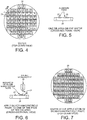
- Figure 4 is a top-down diagram of a silicon wafer 25 of power field effect transistor devices.
- the square of wafer area that will form each power field effect transistor die has both a smaller square gate electrode pad and a larger rectangular source electrode pad. These pads are located on the upper surface of the wafer.
- square die area 26 has a smaller gate electrode pad 27 and a larger source electrode pad 28.
- the entire backside of the wafer (not shown) is covered with backside metallization. After sectioning of the wafer into individual power field effect transistor devices, this backside metal will form the collector electrodes of the devices.
- Figure 5 is a cross-sectional side view of a part of the wafer 25 of Figure 4 taken along sectional line A-A in Figure 4 .
- the leftmost two vertical dashed lines indicate where the left edge of die 26 will be after wafer sectioning.
- the rightmost two vertical dashed lines indicate where the right edge of die 26 will be.
- the pads 27 and 28 at this point in the semiconductor fabrication process are aluminum pads. There is no other metal layer formed on or over the top of these aluminum pads. Due to the aluminum being in the presence of oxygen in the air, the aluminum material of each pad is covered by a thin native aluminum oxide layer.
- Figure 6 is a cross-sectional side view of a subsequent step in the semiconductor fabrication process.
- An amount 29 of silver nanoparticle paste is deposited onto the larger source electrode pad 28 using a micronozzle 30.
- Each larger source electrode pad of the wafer receives a corresponding similar amount of silver nanoparticle paste.
- No silver nanoparticle paste is deposited elsewhere on the wafer.
- the ink-jet micronozzle is scanned back and forth across the wafer and the micronozzle is controlled to emit microdots 24 of the silver nanoparticle paste onto only selected parts of the wafer, the source electrode pads.
- Figure 7 is a top-down diagram of wafer 25 after the deposition of the amounts of silver nanoparticle paste.
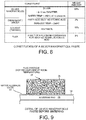
- Figure 8 is a table that sets forth the constituents of the silver nanoparticle paste. The listed weight percentages and temperatures are approximate. The constituents set forth in the table are only for one suitable silver nanoparticle paste that can be used. Other silver nanoparticle pastes can be used and are commercially available from numerous manufacturers.
- suitable silver nanoparticle pastes, and on the silver nanoparticle paste of Figure 8 in particular, and on how to deposit and sinter the paste see: U.S. Patent Application Serial No. 13/490,459 , entitled "Solderless Die Attach To A Direct Bonded Aluminum Substrate, filed June 7, 2012, by Nathan.
- Figure 9 is a cross-sectional side view diagram of amount 29 of the silver nanoparticle paste of Figure 6 after it has been microjetted onto pad 28 and before sintering.
- the hollow circle symbols in Figure 9 represent particles of silver.
- Each silver nanoparticle is coated with the dispersant/binder.
- the dispersant/binder and the thinner of the paste serve to keep the silver particles evenly dispersed in the paste volume.
- the diagram is not to scale but rather is schematically shown to better illustrate the sintering process.
- Layer 30 is a thin layer of native aluminum oxide.
- the dark dots, of which dark dot 31 is one, are particles of flux in the present example where the silver nanoparticle paste of Figure 8 is employed.
- Figure 10 is a cross-sectional side view that illustrates the amount 29 of paste midway through the sintering process.
- the thinner evaporates. This results in a somewhat more dense packing of the nanoparticles as illustrated.
- the temperature is increased further to approximately 200°C.
- the type of dispersant/binder is selected so that the dispersant/binder coating separates from the silver particles and burns out at this 200°C elevated temperature, but before actual sintering takes place at a higher sintering temperature of 250°C.
- the dispersant and the binder involve organic molecules involving carbon chains of twelve or more carbon atoms, whereas the thinner is an organic molecule that has carbon chains of approximately three carbon atoms.
- these and/or other constituents of the paste may decompose to form reactive compounds and acids. These reactive compounds and acids assist in penetrating, cleaning and/or removing oxides from the surface upon which the paste is disposed.
- the temperature is increased to the higher sintering temperature of 250°C.
- the sintering 250°C temperature causes the silver nanoparticles to densify and to sinter together.
- the sintering temperature depends on the size of the nanoparticles and the compaction pressure applied during sintering. In the present example, no compaction pressure is applied.
- Figure 11 is a cross-sectional side view of a resulting sintered silver structure 31.
- the sintered silver structure 31 is also mechanically bonded to the pad.
- the precise manner of mechanical bonding is not fully understood, but it is believed that some of the small silver nanoparticles in their presintered state fit down into small cracks and imperfections in aluminum 28. These embedded particles are then sintered in place so that they are bonded to one another and to other nanoparticles of the larger sintered feature above. Due to these sintered extensions that are anchored into the cracks in aluminum 28, the resulting monolithic sintered structure 31 grasps and is bonded to aluminum pad 28. After the sintering process, the wafer is sectioned into individual power field effect device dice.
- Figure 12 is a perspective view of one of the power field effect transistor dies 26.
- Sintered silver structure 31 is disposed on the source electrode pad 28. There is no sintered silver feature disposed on or over gate electrode pad 27. At this point in the process, gate electrode pad 27 is aluminum, and is covered by a thin layer of native aluminum oxide.
- Figure 13 shows how the die 26 is then incorporated into a packaged power field effect transistor device 32.
- the injection molded encapsulant of the packaged device 32 is not shown in the illustration of Figure 13 .
- a DBA (Direct Bonded Aluminum) substrate structure 33 is manufactured by pressing aluminum plates onto the front and back of a thin ceramic panel under adequate pressure and temperature.
- the ceramic panel may, for example, be 5.6 inches wide by 7.7 inches long, and may be 0.63 mm thick.
- Each of the aluminum plates may be 0.30 mm thick.
- the aluminum plates are patterned and etched to form individual aluminum islands. Separate amounts of silver nanoparticle paste are formed by microjetting microdots of paste onto the panel in selected places in order to form silver die attach structures that will later receive the dice.
- the DBA panel assembly is then sintered so that the volumes of silver nanoparticle paste are sintered to form individual silver die attach structures.
- the DBA panel assembly is then cut into sections to form individual DBAs.
- One such DBA 33 is illustrated in Figure 13 .
- the top aluminum plate has been patterned and etched to form two aluminum islands 34 and 35.
- Reference numeral 31 identifies one of the silver die attach structures.
- a row of such DBAs is attached to a leadframe.
- the ends of the leads of the leadframe may, for example, be ultrasonically bonded to the DBAs.
- the silvered backsides of dies are direct silver-to-silver die attached to corresponding ones of the silver die attach structures of the DBAs. In this way, one die is attached to each DBA without the use of any soft solder.
- a high current clip is provided to electrically connect the sintered silver structure on the source electrode pad to an appropriate one of the leads of the leadframe.
- Reference numeral 37 identifies one such clip in the illustration of Figure 13 .
- the connection from this lip 37 to lead 38 is made via one of the aluminum islands 34.
- a first end of clip 37 is ultrasonically attached to aluminum island 34.
- a second end of clip 37 is soft soldered to sintered silver structure 31 on the source electrode pad 28.
- Each of the dies of the leadframe assembly is provided for clips in this fashion.
- the gate electrode pads of the dies have no silver structures on them. Each of these aluminum pads is provided with a wire bond, thereby attaching the non-silvered gate pad to an appropriate one of the leads.
- a first end of wire bond 39 is ultrasonically wire bonded to aluminum gate pad 27.
- a second end of wire bond 39 is ultrasonically wire bonded to an end of lead 40.
- the backside of the die is connected via silver-to-silver die attach to aluminum island 35 and to lead 41.
- an amount of resin encapsulant 42 (see Figure 14 ) is injection molded over each die of the leadframe assembly in conventional fashion.
- the leadframe assembly is then lead formed and lead trimmed, thereby forming individual packaged power field effect transistor devices.
- Figure 14 is a cross-sectional side view of packaged power field effect transistor device 32.
- Reference numeral 42 identifies the injection molded plastic of the package.
- Reference numeral 43 identifies soft solder that attaches the clip 37 to sintered silver structure 31.
- Figure 15 is a simplified perspective view of a packaged power field effect transistor device 46 (encapsulant not shown) similar to the packaged power field effect transistor device 32 of Figure 13 , except that the packaged power field effect transistor device of Figure 15 employs a different style of clip structure.
- the clip structure of Figure 15 involves a post 44 and a clip 45.
- the silver nanoparticle paste includes flux particles that assist in penetrating the native aluminum oxide on the source electrode pad.
- the silver nanoparticle paste used has no such particles.
- the native aluminum oxide on the pad Prior to deposition of each amount of silver nanoparticle paste on a pad, the native aluminum oxide on the pad is removed by blasting the pad with a stream of abrasive particles.
- the micro-jet head is fitted with two micro-nozzles and a vacuum nozzle for this purpose.
- the micro-jet head is precisely controlled to move in the X, Y and Z dimensions as is known in the micro-jetting arts.
- the micro-nozzle blasts the stream of abrasive particles with a suitable high velocity at the selected localized area of the aluminum source electrode pad.
- the vacuum nozzle is positioned to remove the spent abrasive particles and other debris after the particles have hit the aluminum surface. In this way a high velocity stream of abrasive particles mechanically blasts away the native aluminum oxide on the source electrode pads. Native aluminum oxide does not immediately regrow on the cleaned area due to the entire leadframe assembly being disposed in the oxygen-free environment.
- an amount of silver nanoparticle paste is deposited onto the cleaned aluminum surfaces of the source pads. This deposition also occurs in the oxygen-free environment such that the leadframe assembly is not subjected to oxygen between the time of native oxide removal until after the time of deposition of the silver nanoparticle paste.
- All of the pads to be provided with silver nanoparticle paste may be cleaned in a first pass and then all the cleaned pads provided with amounts of silver nanoparticle paste in a second pass, or alternatively each pad to be provided with silver nanoparticle paste may be individually cleaned and then provided with paste, one by one.
- the entire leadframe assembly is then heated to sinter the amounts of nanoparticle paste on the source pads. The remainder of the fabrication process is the same as described above with respect to the power field effect transistor device 32 of Figure 13 .
- Figure 16 is a flowchart of a method of forming a packaged power field effect transistor device.
- a plurality of separate amounts of silver nanoparticle paste are formed (step 101) on the top-side of a wafer such that there is an amount of silver nanoparticle paste on a first aluminum pad (for example, a source pad) and such that there is no silver nanoparticle paste on a second aluminum pad (for example, a gate pad).
- the first and second aluminum pads are pads for a single discrete field effect transistor.
- the amount of silver nanoparticle paste is then sintered (step 102), along with many other such amounts of silver nanoparticle paste on the wafer, so that the amount of silver nanoparticle paste becomes a sintered silver structure disposed on the first aluminum pad.
- the wafer is diced (step 103) thereby forming power field effect transistor dies.
- the first aluminum pad and the second aluminum pad are pads of one of the dies.
- the first aluminum pad is covered, at least partly, by the sintered silver structure.
- a clip is attached (step 104) to the sintered silver structure.
- the clip forms a part of an electrical connection between the first pad (the silvered source pad) and a first lead of a package.
- a bond wire is attached (step 105) by conventional ultrasonic wire bonding to the second pad.
- the bond wire forms a part of an electrical connection between the bond pad (the non-silvered pad) and a second lead of the package.
- the assembly is then overmolded with plastic encapsulant and is lead formed and lead trimmed, thereby forming the package power field effect transistor device.
Landscapes
- Die Bonding (AREA)
- Wire Bonding (AREA)
Abstract
Description
- The described embodiments relate to power field effect transistor devices.
-
Figure 1 (Prior Art) is a simplified cross-sectional diagram of an old power bipolar transistor structure 1 that was used in the early days of bipolar transistors. The backside of the die is covered with a solderable metal. In the illustrated example, the backside surface of a wafer of devices is covered with alayer 2 of aluminum or titanium. Alayer 3 of nickel is then formed over the aluminum or titanium to act as a barrier. Alayer 4 of silver or gold is then formed by an evaporative deposition process onto the layer of nickel. Thereafter the wafer is diced so that each die has the layers of backside metal as illustrated inFigure 1 . The silver orgold layer 4 is then bonded to asubstrate 5 of a package using an amount ofsoft solder 6. The backside metal structure forms the collector electrode of the bipolar device. An emitter electrode 7 and a base electrode 8 are disposed on the topside of the die. Each electrode involves analuminum layer 9, which is covered by atitanium layer 10, which in turn is covered by a barrier layer ofnickel 11, which in turn is covered by asilver layer 12. These layers are patterned and etched to form the emitter and base electrodes. -
Figure 2 (Prior Art) illustrates the topside emitter electrode 7 and the topside base electrode 8. Afirst post 15 and associatedclip 16 provide an electrical contact and connection from the emitter electrode 7 to a conductor in the package. Asecond post 17 and associatedclip 18 provide an electrical contact and connection from the base electrode 8 to another conductor in the package. The clips are attached to the silver on the top of die using amounts ofsoft solder 18. - With the advent of power field effect transistors, bond wires and wire bonding was used to make electrical connections between the gate and source pads on the die and associated conductors in the package. Clips were typically not used because the geometries of the pads on the die were too tight, and a clip may have shorted the pads together and caused other problems and failures. Currents were typically less than 50 amperes through a pad and were not as great as in the part power devices that were packaged in the manner illustrated in
Figure 1 . A prior conventional thyristor, for example, may have been required to conduct 500 amperes through an electrode. Accordingly, due to the lower current requirements of the early field effect transistors, bond wires were adequate. Over the years since the advent of power field effect transistors, however, currents have steadily increased. To accommodate the increased currents, more and more bond wires have been provided to handle more and more current. -
Figure 3 (Prior Art) is a very simplified illustration intended to show that a greatmany bond wires 19 may be provided between thesource electrode pad 20 of a power fieldeffect transistor device 21 and its package.Fewer bond wires 22 may be provided for the lower currentgate electrode pad 23, but there still may be multiple bond wires provided for this connection. It is now often common to have twenty or thirty bond wires attached to the source electrode pad in some high current power field effect transistor devices. Having this many bond wires on a single pad may introduce crowding problems and other assembly problems. The use of bond wires is nonetheless desirable due to the flexibility of how the connections can be made. - The invention is defined by the features of the independent claims. The dependent claims are directed to preferred embodiments of the invention. A packaged power field effect transistor device includes a power field effect transistor die, a DBA (Direct Bonded Aluminum) substrate, a clip, a wire bond, and a plurality of leads. The die, the clip, the wire bond, and ends of the leads are overmolded with an amount of encapsulant. A top plate of the DBA within the package is patterned to form a plurality of metal plate islands. A sintered silver feature is disposed on one of the metal plate islands of the DBA. A silvered backside of the die is backside bonded in a silver-to-silver solderless die attach process to the sintered silver structure of the DBA.
- The upper surface of the die includes a first aluminum pad (a source pad) and a second aluminum pad (a gate pad). A sintered silver structure is disposed on the first aluminum pad, but there is no sintered silver structure disposed on the second aluminum pad. A first end of the high current clip is attached to another metal island of the DBA. The other metal island in turn is coupled to a first lead of package. A second end of the clip is attached to the sintered silver structure on the first aluminum pad (the source pad) using an amount of soft softer. The second aluminum pad (the gate pad) is connected via a wire bond to a second lead of the package. The wire bond is attached to the second aluminum pad in conventional fashion using an ultrasonic wire bond welding process.
- During manufacturing of the die, a wafer includes a plurality of regions that after wafer sectioning will become individual power field effect transistor dies. A source aluminum pad and a gate aluminum pad are disposed on the upper surface of each of these regions. In a microjetting process, individual amounts of silver nanoparticle paste are selectively deposed only onto the source pads such that no silver nanoparticle paste is deposited onto the gate pads. The entire wafer is microjetted in this way. The term "silver nanoparticle" is used in a general way here, and may describe sinterable pastes having larger particles of silver as long as the silver particles can be satisfactorily sintered together at low enough temperatures that the underlying field effect transistor is not damaged.
- The wafer and the amounts of silver nanoparticle paste are then heated, thereby sintering the amounts of silver nanoparticle paste into individual sintered silver structures. As a result, each aluminum source pad is covered by its own separate sintered silver structure, but there are no sintered silver structures over the gate pads. The wafer is then diced to form the power field effect transistor dies that are then incorporated into the power field effect transistor device packages.
- Further details and embodiments and techniques are described in the detailed description below. This summary does not purport to define the invention. The invention is defined by the claims.
- The accompanying drawings, where like numerals indicate like components, illustrate embodiments of the invention.
-
Figure 1 (Prior Art) is a cross-sectional side view of a bipolar transistor structure used in the early days of power bipolar devices. -
Figure 2 (Prior Art) is a top-down perspective view of the old bipolar transistor structure ofFigure 1 . -
Figure 3 (Prior Art) is a diagram that illustrates how a high current pad of a contemporary field effect transistor device may be required to have many wire bonds to carry the necessary current to/from the high current pad. -
Figure 4 is a top-down diagram of a wafer at one point in the manufacturing of a power field effect transistor die in accordance with one novel aspect. -
Figure 5 is a simplified cross-sectional side view of a part of the wafer ofFigure 4 . -
Figure 6 is a view of the part of the wafer ofFigure 5 during the microjetting of an amount of silver nanoparticle paste onto a source pad. -
Figure 7 is a top-down diagram of the wafer ofFigure 4 after all the source pads of the wafer have been covered with individual amounts of silver nanoparticle paste. -
Figure 8 is a table that sets forth the constituents of the silver nanoparticle paste applied inFigure 6 . -
Figure 9 is a cross-sectional side view of an amount of silver nanoparticle paste disposed on a source pad before sintering. -
Figure 10 is a cross-sectional side view of the silver nanoparticle paste ofFigure 9 part way through the sintering process. -
Figure 11 is a cross-sectional side view of the silver nanoparticle paste ofFigure 9 after sintering has been completed. -
Figure 12 is a simplified perspective view of a power field effect transistor die, where a sintered silver structure is disposed on the source pad of the die, but where no sintered silver structure is disposed on the gate pad of the die. -
Figure 13 is a simplified perspective view of a packaged power field effect transistor device that includes the die ofFigure 12 . -
Figure 14 is a cross-sectional side view of the packaged power field effect transistor device ofFigure 13 . -
Figure 15 is a simplified perspective view of a packaged power field effect transistor device that employs another style of clip in accordance with another novel aspect. -
Figure 16 is a flowchart of a method in accordance with one novel aspect. - Reference will now be made in detail to some embodiments of the invention, examples of which are illustrated in the accompanying drawings. In the description and claims below, when a first object is referred to as being disposed "over" or "on" a second object, it is to be understood that the first object can be directly on the second object, or an intervening object may be present between the first and second objects. Similarly, terms such as "front", "back", "top" and "bottom" are used herein to describe relative orientations between different parts of the structure being described, and it is to be understood that the overall structure being described can actually be oriented in any way in three-dimensional space.
-
Figure 4 is a top-down diagram of asilicon wafer 25 of power field effect transistor devices. At the point in the fabrication process of the devices, all diffusion steps and the lower level metallization and interconnect steps have been performed. The square of wafer area that will form each power field effect transistor die has both a smaller square gate electrode pad and a larger rectangular source electrode pad. These pads are located on the upper surface of the wafer. For example,square die area 26 has a smallergate electrode pad 27 and a largersource electrode pad 28. The entire backside of the wafer (not shown) is covered with backside metallization. After sectioning of the wafer into individual power field effect transistor devices, this backside metal will form the collector electrodes of the devices. -
Figure 5 is a cross-sectional side view of a part of thewafer 25 ofFigure 4 taken along sectional line A-A inFigure 4 . The leftmost two vertical dashed lines indicate where the left edge ofdie 26 will be after wafer sectioning. The rightmost two vertical dashed lines indicate where the right edge ofdie 26 will be. Thepads -
Figure 6 is a cross-sectional side view of a subsequent step in the semiconductor fabrication process. Anamount 29 of silver nanoparticle paste is deposited onto the largersource electrode pad 28 using amicronozzle 30. Each larger source electrode pad of the wafer receives a corresponding similar amount of silver nanoparticle paste. No silver nanoparticle paste is deposited elsewhere on the wafer. There is no silver nanoparticle paste deposited onto any of the gate electrode pads. The ink-jet micronozzle is scanned back and forth across the wafer and the micronozzle is controlled to emitmicrodots 24 of the silver nanoparticle paste onto only selected parts of the wafer, the source electrode pads. -
Figure 7 is a top-down diagram ofwafer 25 after the deposition of the amounts of silver nanoparticle paste. -
Figure 8 is a table that sets forth the constituents of the silver nanoparticle paste. The listed weight percentages and temperatures are approximate. The constituents set forth in the table are only for one suitable silver nanoparticle paste that can be used. Other silver nanoparticle pastes can be used and are commercially available from numerous manufacturers. For additional information on suitable silver nanoparticle pastes, and on the silver nanoparticle paste ofFigure 8 in particular, and on how to deposit and sinter the paste, see:U.S. Patent Application Serial No. 13/490,459 -
Figure 9 is a cross-sectional side view diagram ofamount 29 of the silver nanoparticle paste ofFigure 6 after it has been microjetted ontopad 28 and before sintering. The hollow circle symbols inFigure 9 represent particles of silver. Each silver nanoparticle is coated with the dispersant/binder. The dispersant/binder and the thinner of the paste serve to keep the silver particles evenly dispersed in the paste volume. The diagram is not to scale but rather is schematically shown to better illustrate the sintering process.Layer 30 is a thin layer of native aluminum oxide. The dark dots, of whichdark dot 31 is one, are particles of flux in the present example where the silver nanoparticle paste ofFigure 8 is employed. -
Figure 10 is a cross-sectional side view that illustrates theamount 29 of paste midway through the sintering process. As the temperature increases to about 150°C, the thinner evaporates. This results in a somewhat more dense packing of the nanoparticles as illustrated. Once the thinner has evaporated, the temperature is increased further to approximately 200°C. The type of dispersant/binder is selected so that the dispersant/binder coating separates from the silver particles and burns out at this 200°C elevated temperature, but before actual sintering takes place at a higher sintering temperature of 250°C. Generally the dispersant and the binder involve organic molecules involving carbon chains of twelve or more carbon atoms, whereas the thinner is an organic molecule that has carbon chains of approximately three carbon atoms. Before burning off, these and/or other constituents of the paste may decompose to form reactive compounds and acids. These reactive compounds and acids assist in penetrating, cleaning and/or removing oxides from the surface upon which the paste is disposed. - After burn out of the organic compounds, the temperature is increased to the higher sintering temperature of 250°C. The sintering 250°C temperature causes the silver nanoparticles to densify and to sinter together. The sintering temperature depends on the size of the nanoparticles and the compaction pressure applied during sintering. In the present example, no compaction pressure is applied.
-
Figure 11 is a cross-sectional side view of a resulting sinteredsilver structure 31. There is good electrical contact between the resulting sinteredsilver structure 31 and the unoxidized aluminum of theunderlying aluminum pad 28. This electrical connection exists throughnative oxide layer 30. Thesintered silver structure 31 is also mechanically bonded to the pad. The precise manner of mechanical bonding is not fully understood, but it is believed that some of the small silver nanoparticles in their presintered state fit down into small cracks and imperfections inaluminum 28. These embedded particles are then sintered in place so that they are bonded to one another and to other nanoparticles of the larger sintered feature above. Due to these sintered extensions that are anchored into the cracks inaluminum 28, the resultingmonolithic sintered structure 31 grasps and is bonded toaluminum pad 28. After the sintering process, the wafer is sectioned into individual power field effect device dice. -
Figure 12 is a perspective view of one of the power field effect transistor dies 26.Sintered silver structure 31 is disposed on thesource electrode pad 28. There is no sintered silver feature disposed on or overgate electrode pad 27. At this point in the process,gate electrode pad 27 is aluminum, and is covered by a thin layer of native aluminum oxide. -
Figure 13 shows how thedie 26 is then incorporated into a packaged power fieldeffect transistor device 32. The injection molded encapsulant of the packageddevice 32 is not shown in the illustration ofFigure 13 . - A DBA (Direct Bonded Aluminum)
substrate structure 33 is manufactured by pressing aluminum plates onto the front and back of a thin ceramic panel under adequate pressure and temperature. The ceramic panel may, for example, be 5.6 inches wide by 7.7 inches long, and may be 0.63 mm thick. Each of the aluminum plates may be 0.30 mm thick. After attachment of the aluminum plates to the ceramic substrate panel, the aluminum plates are patterned and etched to form individual aluminum islands. Separate amounts of silver nanoparticle paste are formed by microjetting microdots of paste onto the panel in selected places in order to form silver die attach structures that will later receive the dice. The DBA panel assembly is then sintered so that the volumes of silver nanoparticle paste are sintered to form individual silver die attach structures. The DBA panel assembly is then cut into sections to form individual DBAs. Onesuch DBA 33 is illustrated inFigure 13 . The top aluminum plate has been patterned and etched to form twoaluminum islands Reference numeral 31 identifies one of the silver die attach structures. - Next, a row of such DBAs is attached to a leadframe. The ends of the leads of the leadframe may, for example, be ultrasonically bonded to the DBAs. After ultrasonic bonding of the DBAs to the leadframe, the silvered backsides of dies are direct silver-to-silver die attached to corresponding ones of the silver die attach structures of the DBAs. In this way, one die is attached to each DBA without the use of any soft solder.
- Next, for each die, a high current clip is provided to electrically connect the sintered silver structure on the source electrode pad to an appropriate one of the leads of the leadframe.
Reference numeral 37 identifies one such clip in the illustration ofFigure 13 . The connection from thislip 37 to lead 38 is made via one of thealuminum islands 34. In the illustration ofFigure 13 , a first end ofclip 37 is ultrasonically attached toaluminum island 34. A second end ofclip 37 is soft soldered tosintered silver structure 31 on thesource electrode pad 28. Each of the dies of the leadframe assembly is provided for clips in this fashion. - The gate electrode pads of the dies have no silver structures on them. Each of these aluminum pads is provided with a wire bond, thereby attaching the non-silvered gate pad to an appropriate one of the leads. In the illustration of
Figure 13 , a first end ofwire bond 39 is ultrasonically wire bonded toaluminum gate pad 27. A second end ofwire bond 39 is ultrasonically wire bonded to an end oflead 40. As explained above, the backside of the die is connected via silver-to-silver die attach toaluminum island 35 and to lead 41. - After clip attachment and wire bonding, an amount of resin encapsulant 42 (see
Figure 14 ) is injection molded over each die of the leadframe assembly in conventional fashion. The leadframe assembly is then lead formed and lead trimmed, thereby forming individual packaged power field effect transistor devices. -
Figure 14 is a cross-sectional side view of packaged power fieldeffect transistor device 32.Reference numeral 42 identifies the injection molded plastic of the package.Reference numeral 43 identifies soft solder that attaches theclip 37 to sinteredsilver structure 31. -
Figure 15 is a simplified perspective view of a packaged power field effect transistor device 46 (encapsulant not shown) similar to the packaged power fieldeffect transistor device 32 ofFigure 13 , except that the packaged power field effect transistor device ofFigure 15 employs a different style of clip structure. The clip structure ofFigure 15 involves apost 44 and aclip 45. - In the fabrication process described above, the silver nanoparticle paste includes flux particles that assist in penetrating the native aluminum oxide on the source electrode pad. In another example, the silver nanoparticle paste used has no such particles. Prior to deposition of each amount of silver nanoparticle paste on a pad, the native aluminum oxide on the pad is removed by blasting the pad with a stream of abrasive particles. The micro-jet head is fitted with two micro-nozzles and a vacuum nozzle for this purpose. The micro-jet head is precisely controlled to move in the X, Y and Z dimensions as is known in the micro-jetting arts. The micro-nozzle blasts the stream of abrasive particles with a suitable high velocity at the selected localized area of the aluminum source electrode pad. The vacuum nozzle is positioned to remove the spent abrasive particles and other debris after the particles have hit the aluminum surface. In this way a high velocity stream of abrasive particles mechanically blasts away the native aluminum oxide on the source electrode pads. Native aluminum oxide does not immediately regrow on the cleaned area due to the entire leadframe assembly being disposed in the oxygen-free environment. Next, an amount of silver nanoparticle paste is deposited onto the cleaned aluminum surfaces of the source pads. This deposition also occurs in the oxygen-free environment such that the leadframe assembly is not subjected to oxygen between the time of native oxide removal until after the time of deposition of the silver nanoparticle paste. All of the pads to be provided with silver nanoparticle paste may be cleaned in a first pass and then all the cleaned pads provided with amounts of silver nanoparticle paste in a second pass, or alternatively each pad to be provided with silver nanoparticle paste may be individually cleaned and then provided with paste, one by one. After the source pads have been microjetted with silver nanoparticle paste, the entire leadframe assembly is then heated to sinter the amounts of nanoparticle paste on the source pads. The remainder of the fabrication process is the same as described above with respect to the power field
effect transistor device 32 ofFigure 13 . -
Figure 16 is a flowchart of a method of forming a packaged power field effect transistor device. A plurality of separate amounts of silver nanoparticle paste are formed (step 101) on the top-side of a wafer such that there is an amount of silver nanoparticle paste on a first aluminum pad (for example, a source pad) and such that there is no silver nanoparticle paste on a second aluminum pad (for example, a gate pad). The first and second aluminum pads are pads for a single discrete field effect transistor. The amount of silver nanoparticle paste is then sintered (step 102), along with many other such amounts of silver nanoparticle paste on the wafer, so that the amount of silver nanoparticle paste becomes a sintered silver structure disposed on the first aluminum pad. Next, the wafer is diced (step 103) thereby forming power field effect transistor dies. The first aluminum pad and the second aluminum pad are pads of one of the dies. The first aluminum pad is covered, at least partly, by the sintered silver structure. There is no sintered silver structure disposed on the second aluminum pad. Subsequently, in the chip assembly process, a clip is attached (step 104) to the sintered silver structure. The clip forms a part of an electrical connection between the first pad (the silvered source pad) and a first lead of a package. A bond wire is attached (step 105) by conventional ultrasonic wire bonding to the second pad. The bond wire forms a part of an electrical connection between the bond pad (the non-silvered pad) and a second lead of the package. The assembly is then overmolded with plastic encapsulant and is lead formed and lead trimmed, thereby forming the package power field effect transistor device. - Although certain specific embodiments are described above for instructional purposes, the teachings of this patent document have general applicability and are not limited to the specific embodiments described above. Accordingly, various modifications, adaptations, and combinations of various features of the described embodiments can be practiced without departing from the scope of the invention as set forth in the claims.
-
- 1. A method of manufacturing a semiconductor die, comprising the steps of:
- (a) forming a plurality of separate amounts of silver nanoparticle paste on a top-side of a wafer such that there is an amount of silver nanoparticle paste on a first aluminum pad and such that there is no silver nanoparticle paste on a second aluminum pad; and
- (b) sintering the amount of silver nanoparticle paste so that the amount of silver nanoparticle paste becomes a sintered silver structure disposed on the first aluminum pad and so that the second aluminum pad is not covered by any sintered silverlayer.
- 2. The method of clause 1, further comprising the step of:
(c) dicing the wafer into a plurality of dice, wherein one of the dice is a die that includes the first aluminum pad that is covered with the sintered silver structure and the second aluminum pad that is not covered by any sintered silver structure. - 3. The method of
claim 2, further comprising the steps of:- (d) attaching a clip to the sintered silver structure on the first pad; and
- (e) attaching a bond wire to the second pad.
- 4. The method of
clause 2, further comprising the step of:
(d) using solder to attach a clip to the sintered silver structure of the first pad. - 5. The method of
clause 2, further comprising the step of:
(d) attaching a back-side of the die to a Direct Bonded Aluminum (DBA) substrate with a solderless silver-to-silver bond. - 6. The method of any one of clauses 1 to 5, wherein there is no non-aluminum metal layer disposed between the first aluminum pad and the amount of silver nanoparticle paste during the forming of step (a), and wherein there is no non-aluminum metal layer disposed on the second aluminum pad during the forming of step (a).
- 7. The method of any one of
clauses 2 to 6, wherein said one of the dice is a power field effect transistor device. - 8. The method of any one of clauses 1 to 7, wherein step (a) includes microjetting the plurality of separate amounts of silver nanoparticle paste onto source electrode pads on the top-side of the wafer.
- 9. The method of any one of clauses 1 to 7, wherein step (a) includes the steps of:
- (a1) directing a stream of abrasive particles at the first aluminum pad thereby removing a layer of native aluminum oxide from the first aluminum pad; and
- (a2) after the removal of the layer of native aluminum oxide of step (a1) then microjetting the amount of silver nanoparticle paste onto the first aluminum pad.
- 10. The method of any one of clauses 1 to 9, wherein the silver nanoparticle paste includes flux particles.
- 11. An assembly comprising:
- a semiconductor die having a first aluminum pad and a second aluminum pad, wherein a sintered silver structure is disposed on the first aluminum pad but wherein there is no sintered silver structure disposed on the second aluminum pad;
- a clip that is attached to the sintered silver structure; and
- a bond wire that is bonded to the second aluminum pad.
- 12. The assembly of
clause 11, further comprising:- a Direct Bonded Aluminum (DBA) substrate that comprises a ceramic substrate member and a plate of aluminum that is direct bonded to the ceramic substrate member; and
- a sintered silver structure that is disposed on the plate of aluminum, wherein
- the semiconductor die has a layer of silver disposed on a backside of the semiconductor die, and
- the layer of silver on the backside of the semiconductor die is direct silver-to-silver bonded to the sintered silver structure on the plate of aluminum.
- 13. The assembly of
clause 12, wherein- the DBA substrate further comprises a second plate of aluminum,
- a first end of the clip is bonded to the second plate of aluminum of the DBA substrate, and
- a second end of the clip is bonded to the sintered silver structure on the first aluminum pad.
- 14. The assembly of
clause 12 or 13, wherein- the semiconductor die is a power field effect transistor device,
- the first aluminum pad is a source pad, and
- the second aluminum pad is a gate pad.
- 15. The assembly of any one of
clauses 11 to 14, wherein the clip is attached with soft solder to the sintered silver structure on the first aluminum pad.
Claims (14)
- A semiconductor die having a first aluminum pad and a second aluminum pad, wherein a sintered silver structure is disposed on the first aluminum pad but wherein there is no sintered silver structure disposed on the second aluminum pad.
- The semiconductor die of claim 1, wherein there is no non-aluminum metal layer disposed between the first aluminum pad and the sintered silver structure.
- The semiconductor die of claim 1 or 2, wherein the semiconductor die is a power field effect transistor device die, wherein the first aluminum pad is a source electrode pad, and wherein the second aluminum pad is a gate electrode pad.
- An assembly comprising:the semiconductor die of any one of claims 1 to 3;a clip that is attached to the sintered silver structure; anda bond wire that is bonded to the second aluminum pad.
- The assembly of claim 4, wherein the clip is attached with soft solder to the sintered silver structure on the first aluminum pad.
- The assembly of claim 4 or 5, further comprising:a direct bonded aluminum (DBA) substrate that comprises a ceramic substrate member and a plate of aluminum that is direct bonded to the ceramic substrate member; anda sintered silver structure that is disposed on the plate of aluminum,wherein the semiconductor die has a layer of silver disposed on a backside of the semiconductor die, andwherein the layer of silver on the backside of the semiconductor die is direct silver-to-silver bonded to the sintered silver structure on the plate of aluminum.
- The assembly of claim 6, wherein the layer of silver is direct silver-to-silver bonded to the sintered silver structure on the plate of aluminum without using any solder.
- The assembly of claim 6 or 7, wherein the DBA further comprises a second plate of aluminum, wherein a first end of the clip is bonded to the second plate of aluminum of the DBA, and wherein a second end of the clip is bonded to the sintered silver structure on the first aluminum pad.
- A method of manufacturing a semiconductor die, comprising the steps of:forming a plurality of separate amounts of silver nanoparticle paste on a top-side of a wafer such that there is an amount of silver nanoparticle paste on a first aluminum pad and such that there is no silver nanoparticle paste on a second aluminum pad;sintering the amount of silver nanoparticle paste so that the amount of silver nanoparticle paste becomes a sintered silver structure disposed on the first aluminum pad and so that the second aluminum pad is not covered by any sintered silver layer; anddicing the wafer into a plurality of dice, wherein one of the dice is the semiconductor die that includes the first aluminum pad that is covered with the sintered silver structure and the second aluminum pad that is not covered by any sintered silver structure.
- The method of claim 9, wherein there is no non-aluminum metal layer disposed between the first aluminum pad and the amount of silver nanoparticle paste during the step of forming, and wherein there is no non-aluminum metal layer disposed on the second aluminum pad during the step of forming.
- The method of claim 9 or 10, wherein the semiconductor die is a power field effect transistor device die.
- The method of any one of claims 9 to 11, wherein the step of forming includes microjetting the plurality of separate amounts of silver nanoparticle paste onto source electrode pads on the top-side of the wafer.
- The method of any one of claims 9 to 12, wherein the step of forming includes the steps of:directing a stream of abrasive particles at the first aluminum pad thereby removing a layer of native aluminum oxide from the first aluminum pad; andafter removal of the layer of native aluminum oxide, microjetting the amount of silver nanoparticle paste onto the first aluminum pad.
- The method of any one of claims 9 to 13, wherein the silver nanoparticle paste includes flux particles.
Applications Claiming Priority (2)
| Application Number | Priority Date | Filing Date | Title |
|---|---|---|---|
| US13/563,703 US8586480B1 (en) | 2012-07-31 | 2012-07-31 | Power MOSFET having selectively silvered pads for clip and bond wire attach |
| EP13177989.4A EP2693474B1 (en) | 2012-07-31 | 2013-07-25 | Method of manufacturing a semiconductor die assembly with a clip bonded to an aluminium pad coated by a sintered silver structure and with a wire bonded to an uncoated aluminium pad |
Related Parent Applications (2)
| Application Number | Title | Priority Date | Filing Date |
|---|---|---|---|
| EP13177989.4A Division EP2693474B1 (en) | 2012-07-31 | 2013-07-25 | Method of manufacturing a semiconductor die assembly with a clip bonded to an aluminium pad coated by a sintered silver structure and with a wire bonded to an uncoated aluminium pad |
| EP13177989.4A Division-Into EP2693474B1 (en) | 2012-07-31 | 2013-07-25 | Method of manufacturing a semiconductor die assembly with a clip bonded to an aluminium pad coated by a sintered silver structure and with a wire bonded to an uncoated aluminium pad |
Publications (2)
| Publication Number | Publication Date |
|---|---|
| EP3742481A2 true EP3742481A2 (en) | 2020-11-25 |
| EP3742481A3 EP3742481A3 (en) | 2021-01-13 |
Family
ID=48948221
Family Applications (2)
| Application Number | Title | Priority Date | Filing Date |
|---|---|---|---|
| EP20174492.7A Pending EP3742481A3 (en) | 2012-07-31 | 2013-07-25 | Semiconductor die with an aluminium pad coated by a sintered silver structure for a clip and with an uncoated aluminium pad for a bond wire and corresponding manufacturing method |
| EP13177989.4A Active EP2693474B1 (en) | 2012-07-31 | 2013-07-25 | Method of manufacturing a semiconductor die assembly with a clip bonded to an aluminium pad coated by a sintered silver structure and with a wire bonded to an uncoated aluminium pad |
Family Applications After (1)
| Application Number | Title | Priority Date | Filing Date |
|---|---|---|---|
| EP13177989.4A Active EP2693474B1 (en) | 2012-07-31 | 2013-07-25 | Method of manufacturing a semiconductor die assembly with a clip bonded to an aluminium pad coated by a sintered silver structure and with a wire bonded to an uncoated aluminium pad |
Country Status (2)
| Country | Link |
|---|---|
| US (2) | US8586480B1 (en) |
| EP (2) | EP3742481A3 (en) |
Families Citing this family (18)
| Publication number | Priority date | Publication date | Assignee | Title |
|---|---|---|---|---|
| US20130175704A1 (en) * | 2012-01-05 | 2013-07-11 | Ixys Corporation | Discrete power transistor package having solderless dbc to leadframe attach |
| WO2014076856A1 (en) * | 2012-11-19 | 2014-05-22 | 富士電機株式会社 | Semiconductor device |
| US8987911B2 (en) * | 2012-12-31 | 2015-03-24 | Ixys Corporation | Silver-to-silver bonded IC package having two ceramic substrates exposed on the outside of the package |
| US9431394B2 (en) * | 2013-08-29 | 2016-08-30 | Infineon Technologies Ag | Power semiconductor package with gate and field electrode leads |
| JP6238121B2 (en) * | 2013-10-01 | 2017-11-29 | ローム株式会社 | Semiconductor device |
| KR102245825B1 (en) | 2014-09-04 | 2021-04-30 | 삼성전자주식회사 | Semiconductor pakage |
| US10847691B2 (en) * | 2014-12-11 | 2020-11-24 | Luminus, Inc. | LED flip chip structures with extended contact pads formed by sintering silver |
| KR101644913B1 (en) * | 2015-01-08 | 2016-08-04 | (주) 루트세미콘 | Semiconductor package by using ultrasonic welding and methods of fabricating the same |
| KR101643332B1 (en) * | 2015-03-20 | 2016-07-27 | 제엠제코(주) | Clip -bonded semiconductor chip package using ultrasonic welding and the manufacturing method thereof |
| US9640466B1 (en) * | 2016-02-24 | 2017-05-02 | Nxp Usa, Inc. | Packaged semiconductor device with a lead frame and method for forming |
| DE102016107287A1 (en) * | 2016-04-20 | 2017-11-09 | Semikron Elektronik Gmbh & Co. Kg | Power semiconductor device and method for operating a power semiconductor device |
| US10872846B2 (en) | 2017-06-22 | 2020-12-22 | Renesas Electronics America Inc. | Solid top terminal for discrete power devices |
| CN109788643B (en) * | 2017-11-10 | 2024-07-30 | 泰连公司 | Aluminum-based weldable contacts |
| US11031364B2 (en) * | 2018-03-07 | 2021-06-08 | Texas Instruments Incorporated | Nanoparticle backside die adhesion layer |
| US12159846B2 (en) * | 2019-07-01 | 2024-12-03 | Texas Instruments Incorporated | Process flow for fabrication of cap metal over top metal with sinter before protective dielectric etch |
| CN110773908A (en) * | 2019-10-28 | 2020-02-11 | 深圳第三代半导体研究院 | Preparation method and sintering method of low-temperature sintered indium-doped nano-silver sintering paste |
| US12539541B2 (en) * | 2020-10-05 | 2026-02-03 | Stmicroelectronics S.R.L. | Silver nanoparticles synthesis method for low temperature and pressure sintering |
| EP4739080A1 (en) * | 2024-10-31 | 2026-05-06 | Nexperia B.V. | A method of manufacturing a plurality of semiconductor devices as well as a corresponding semiconductor device |
Family Cites Families (25)
| Publication number | Priority date | Publication date | Assignee | Title |
|---|---|---|---|---|
| US3254276A (en) * | 1961-11-29 | 1966-05-31 | Philco Corp | Solid-state translating device with barrier-layers formed by thin metal and semiconductor material |
| GB1297046A (en) * | 1969-08-25 | 1972-11-22 | ||
| JP3557143B2 (en) * | 2000-01-19 | 2004-08-25 | 三洋電機株式会社 | Switching element bare chip mounting structure |
| JP2002110750A (en) * | 2000-09-29 | 2002-04-12 | Mitsubishi Electric Corp | Electronic component manufacturing method and connection structure |
| US6670216B2 (en) * | 2001-10-31 | 2003-12-30 | Ixys Corporation | Method for manufacturing a power semiconductor device and direct bonded substrate thereof |
| US7378342B2 (en) * | 2004-08-27 | 2008-05-27 | Micron Technology, Inc. | Methods for forming vias varying lateral dimensions |
| JP2006190728A (en) * | 2005-01-04 | 2006-07-20 | Mitsubishi Electric Corp | Power semiconductor device |
| JP2006202938A (en) * | 2005-01-20 | 2006-08-03 | Kojiro Kobayashi | Semiconductor device and manufacturing method thereof |
| WO2007122925A1 (en) * | 2006-04-24 | 2007-11-01 | Murata Manufacturing Co., Ltd. | Electronic component, electronic component device using same, and method for manufacturing same |
| WO2008044537A1 (en) * | 2006-10-05 | 2008-04-17 | Nec Corporation | Semiconductor package and method for producing semiconductor package |
| DE102007022338B4 (en) * | 2007-07-26 | 2013-12-05 | Semikron Elektronik Gmbh & Co. Kg | Manufacturing method for a power semiconductor device with metal contact layer |
| JP5331321B2 (en) * | 2007-08-31 | 2013-10-30 | ゴールドチャームリミテッド | Manufacturing method of display device |
| US8642394B2 (en) * | 2008-01-28 | 2014-02-04 | Infineon Technologies Ag | Method of manufacturing electronic device on leadframe |
| US9017808B2 (en) * | 2008-03-17 | 2015-04-28 | The Research Foundation For The State University Of New York | Composite thermal interface material system and method using nano-scale components |
| US20110114914A1 (en) * | 2008-07-25 | 2011-05-19 | Hideaki Numata | Field effect transistor and circuit device |
| US8410590B2 (en) * | 2008-09-30 | 2013-04-02 | Infineon Technologies Ag | Device including a power semiconductor chip electrically coupled to a leadframe via a metallic layer |
| JP5156658B2 (en) * | 2009-01-30 | 2013-03-06 | 株式会社日立製作所 | Electronic components for LSI |
| JP5304508B2 (en) * | 2009-05-15 | 2013-10-02 | 三菱マテリアル株式会社 | Conductive composition |
| JP2011014556A (en) * | 2009-06-30 | 2011-01-20 | Hitachi Ltd | Semiconductor device and method of manufacturing the same |
| DE102009029577B3 (en) * | 2009-09-18 | 2011-04-28 | Infineon Technologies Ag | Process for producing a high-temperature-resistant power semiconductor module |
| JP2011086743A (en) * | 2009-10-15 | 2011-04-28 | Mitsubishi Electric Corp | Power semiconductor device and method for manufacturing the power semiconductor device |
| JP5185956B2 (en) * | 2010-01-06 | 2013-04-17 | 三菱電機株式会社 | Power semiconductor device |
| EP2442367B1 (en) * | 2010-10-14 | 2014-07-16 | Rohm and Haas Electronic Materials LLC | Improved method for forming metal contacts |
| US8643165B2 (en) * | 2011-02-23 | 2014-02-04 | Texas Instruments Incorporated | Semiconductor device having agglomerate terminals |
| US8716864B2 (en) * | 2012-06-07 | 2014-05-06 | Ixys Corporation | Solderless die attach to a direct bonded aluminum substrate |
-
2012
- 2012-07-31 US US13/563,703 patent/US8586480B1/en active Active
-
2013
- 2013-07-25 EP EP20174492.7A patent/EP3742481A3/en active Pending
- 2013-07-25 EP EP13177989.4A patent/EP2693474B1/en active Active
- 2013-10-23 US US14/061,610 patent/US8653667B1/en active Active
Also Published As
| Publication number | Publication date |
|---|---|
| EP3742481A3 (en) | 2021-01-13 |
| EP2693474A2 (en) | 2014-02-05 |
| US8653667B1 (en) | 2014-02-18 |
| US20140042624A1 (en) | 2014-02-13 |
| US8586480B1 (en) | 2013-11-19 |
| EP2693474A3 (en) | 2014-10-08 |
| EP2693474B1 (en) | 2020-11-25 |
Similar Documents
| Publication | Publication Date | Title |
|---|---|---|
| EP2693474B1 (en) | Method of manufacturing a semiconductor die assembly with a clip bonded to an aluminium pad coated by a sintered silver structure and with a wire bonded to an uncoated aluminium pad | |
| US9111782B2 (en) | Solderless die attach to a direct bonded aluminum substrate | |
| US11387162B2 (en) | Discrete power transistor package having solderless DBC to leadframe attach | |
| US8252632B2 (en) | Semiconductor device and manufacturing method of the same | |
| CN103875067B (en) | Method for forming connections between metal moldings and power semiconductors for bonding to thick wiring or strips | |
| US9082879B2 (en) | Silver-to-silver bonded IC package having two ceramic substrates exposed on the outside of the package | |
| JP3796016B2 (en) | Semiconductor device | |
| KR20050044518A (en) | Compound semiconductor light emitting device and its manufacturing method | |
| JPH11186301A (en) | Method for manufacturing semiconductor device | |
| TWI339425B (en) | Thin gaas die with copper back-metal structure | |
| JP4408475B2 (en) | Semiconductor devices that do not use bonding wires | |
| JP3928488B2 (en) | Semiconductor device and manufacturing method thereof | |
| CN101192551B (en) | Gold/Silicon Eutectic Die Bonding Method | |
| CN114078716B (en) | Semiconductor devices and their manufacturing methods | |
| WO2020127442A2 (en) | Semiconductor module having a semiconductor and a housing partially enclosing the semiconductor | |
| JP2007150342A (en) | Semiconductor device and manufacturing method thereof | |
| CN204696104U (en) | A kind of system-level MEMS complex carries chip package | |
| JP3203228B2 (en) | Semiconductor device and manufacturing method thereof | |
| JPH09293905A (en) | Semiconductor device and manufacturing method thereof | |
| JP4979661B2 (en) | Manufacturing method of semiconductor device | |
| JP3098194B2 (en) | Method for manufacturing silicon semiconductor diode chip in which fully open PN junction is passivated with glass | |
| CN106252318B (en) | Plant ball process and structure | |
| JPH09116090A (en) | Power semiconductor module | |
| EP4739080A1 (en) | A method of manufacturing a plurality of semiconductor devices as well as a corresponding semiconductor device |
Legal Events
| Date | Code | Title | Description |
|---|---|---|---|
| PUAI | Public reference made under article 153(3) epc to a published international application that has entered the european phase |
Free format text: ORIGINAL CODE: 0009012 |
|
| STAA | Information on the status of an ep patent application or granted ep patent |
Free format text: STATUS: THE APPLICATION HAS BEEN PUBLISHED |
|
| AC | Divisional application: reference to earlier application |
Ref document number: 2693474 Country of ref document: EP Kind code of ref document: P |
|
| AK | Designated contracting states |
Kind code of ref document: A2 Designated state(s): AL AT BE BG CH CY CZ DE DK EE ES FI FR GB GR HR HU IE IS IT LI LT LU LV MC MK MT NL NO PL PT RO RS SE SI SK SM TR |
|
| PUAL | Search report despatched |
Free format text: ORIGINAL CODE: 0009013 |
|
| AK | Designated contracting states |
Kind code of ref document: A3 Designated state(s): AL AT BE BG CH CY CZ DE DK EE ES FI FR GB GR HR HU IE IS IT LI LT LU LV MC MK MT NL NO PL PT RO RS SE SI SK SM TR |
|
| RIC1 | Information provided on ipc code assigned before grant |
Ipc: H01L 23/488 20060101ALI20201207BHEP Ipc: H01L 23/373 20060101ALN20201207BHEP Ipc: H01L 23/495 20060101ALN20201207BHEP Ipc: H01L 23/485 20060101AFI20201207BHEP Ipc: H01L 21/60 20060101ALI20201207BHEP Ipc: H01L 23/49 20060101ALI20201207BHEP |
|
| STAA | Information on the status of an ep patent application or granted ep patent |
Free format text: STATUS: REQUEST FOR EXAMINATION WAS MADE |
|
| 17P | Request for examination filed |
Effective date: 20210709 |
|
| RBV | Designated contracting states (corrected) |
Designated state(s): AL AT BE BG CH CY CZ DE DK EE ES FI FR GB GR HR HU IE IS IT LI LT LU LV MC MK MT NL NO PL PT RO RS SE SI SK SM TR |