EP3734673B1 - Lichtquellensystem und beleuchtungsvorrichtung - Google Patents
Lichtquellensystem und beleuchtungsvorrichtung Download PDFInfo
- Publication number
- EP3734673B1 EP3734673B1 EP18895195.8A EP18895195A EP3734673B1 EP 3734673 B1 EP3734673 B1 EP 3734673B1 EP 18895195 A EP18895195 A EP 18895195A EP 3734673 B1 EP3734673 B1 EP 3734673B1
- Authority
- EP
- European Patent Office
- Prior art keywords
- light
- source system
- light source
- lasers
- wavelength conversion
- Prior art date
- Legal status (The legal status is an assumption and is not a legal conclusion. Google has not performed a legal analysis and makes no representation as to the accuracy of the status listed.)
- Active
Links
Images



Classifications
-
- F—MECHANICAL ENGINEERING; LIGHTING; HEATING; WEAPONS; BLASTING
- F21—LIGHTING
- F21V—FUNCTIONAL FEATURES OR DETAILS OF LIGHTING DEVICES OR SYSTEMS THEREOF; STRUCTURAL COMBINATIONS OF LIGHTING DEVICES WITH OTHER ARTICLES, NOT OTHERWISE PROVIDED FOR
- F21V29/00—Protecting lighting devices from thermal damage; Cooling or heating arrangements specially adapted for lighting devices or systems
- F21V29/10—Arrangement of heat-generating components to reduce thermal damage, e.g. by distancing heat-generating components from other components to be protected
-
- H—ELECTRICITY
- H01—ELECTRIC ELEMENTS
- H01S—DEVICES USING THE PROCESS OF LIGHT AMPLIFICATION BY STIMULATED EMISSION OF RADIATION [LASER] TO AMPLIFY OR GENERATE LIGHT; DEVICES USING STIMULATED EMISSION OF ELECTROMAGNETIC RADIATION IN WAVE RANGES OTHER THAN OPTICAL
- H01S5/00—Semiconductor lasers
- H01S5/005—Optical components external to the laser cavity, specially adapted therefor, e.g. for homogenisation or merging of the beams or for manipulating laser pulses, e.g. pulse shaping
- H01S5/0087—Optical components external to the laser cavity, specially adapted therefor, e.g. for homogenisation or merging of the beams or for manipulating laser pulses, e.g. pulse shaping for illuminating phosphorescent or fluorescent materials, e.g. using optical arrangements specifically adapted for guiding or shaping laser beams illuminating these materials
-
- F—MECHANICAL ENGINEERING; LIGHTING; HEATING; WEAPONS; BLASTING
- F21—LIGHTING
- F21V—FUNCTIONAL FEATURES OR DETAILS OF LIGHTING DEVICES OR SYSTEMS THEREOF; STRUCTURAL COMBINATIONS OF LIGHTING DEVICES WITH OTHER ARTICLES, NOT OTHERWISE PROVIDED FOR
- F21V7/00—Reflectors for light sources
- F21V7/04—Optical design
- F21V7/05—Optical design plane
-
- F—MECHANICAL ENGINEERING; LIGHTING; HEATING; WEAPONS; BLASTING
- F21—LIGHTING
- F21V—FUNCTIONAL FEATURES OR DETAILS OF LIGHTING DEVICES OR SYSTEMS THEREOF; STRUCTURAL COMBINATIONS OF LIGHTING DEVICES WITH OTHER ARTICLES, NOT OTHERWISE PROVIDED FOR
- F21V9/00—Elements for modifying spectral properties, polarisation or intensity of the light emitted, e.g. filters
- F21V9/30—Elements containing photoluminescent material distinct from or spaced from the light source
-
- G—PHYSICS
- G02—OPTICS
- G02B—OPTICAL ELEMENTS, SYSTEMS OR APPARATUS
- G02B27/00—Optical systems or apparatus not provided for by any of the groups G02B1/00 - G02B26/00, G02B30/00
- G02B27/10—Beam splitting or combining systems
- G02B27/12—Beam splitting or combining systems operating by refraction only
- G02B27/126—The splitting element being a prism or prismatic array, including systems based on total internal reflection
-
- G—PHYSICS
- G02—OPTICS
- G02B—OPTICAL ELEMENTS, SYSTEMS OR APPARATUS
- G02B27/00—Optical systems or apparatus not provided for by any of the groups G02B1/00 - G02B26/00, G02B30/00
- G02B27/28—Optical systems or apparatus not provided for by any of the groups G02B1/00 - G02B26/00, G02B30/00 for polarising
- G02B27/283—Optical systems or apparatus not provided for by any of the groups G02B1/00 - G02B26/00, G02B30/00 for polarising used for beam splitting or combining
-
- H—ELECTRICITY
- H01—ELECTRIC ELEMENTS
- H01S—DEVICES USING THE PROCESS OF LIGHT AMPLIFICATION BY STIMULATED EMISSION OF RADIATION [LASER] TO AMPLIFY OR GENERATE LIGHT; DEVICES USING STIMULATED EMISSION OF ELECTROMAGNETIC RADIATION IN WAVE RANGES OTHER THAN OPTICAL
- H01S5/00—Semiconductor lasers
- H01S5/02—Structural details or components not essential to laser action
- H01S5/024—Arrangements for thermal management
- H01S5/02476—Heat spreaders, i.e. improving heat flow between laser chip and heat dissipating elements
-
- H—ELECTRICITY
- H01—ELECTRIC ELEMENTS
- H01S—DEVICES USING THE PROCESS OF LIGHT AMPLIFICATION BY STIMULATED EMISSION OF RADIATION [LASER] TO AMPLIFY OR GENERATE LIGHT; DEVICES USING STIMULATED EMISSION OF ELECTROMAGNETIC RADIATION IN WAVE RANGES OTHER THAN OPTICAL
- H01S5/00—Semiconductor lasers
- H01S5/40—Arrangement of two or more semiconductor lasers, not provided for in groups H01S5/02 - H01S5/30
- H01S5/4025—Array arrangements, e.g. constituted by discrete laser diodes or laser bar
- H01S5/4031—Edge-emitting structures
- H01S5/4056—Edge-emitting structures emitting light in more than one direction
-
- H—ELECTRICITY
- H10—SEMICONDUCTOR DEVICES; ELECTRIC SOLID-STATE DEVICES NOT OTHERWISE PROVIDED FOR
- H10H—INORGANIC LIGHT-EMITTING SEMICONDUCTOR DEVICES HAVING POTENTIAL BARRIERS
- H10H20/00—Individual inorganic light-emitting semiconductor devices having potential barriers, e.g. light-emitting diodes [LED]
- H10H20/80—Constructional details
-
- F—MECHANICAL ENGINEERING; LIGHTING; HEATING; WEAPONS; BLASTING
- F21—LIGHTING
- F21Y—INDEXING SCHEME ASSOCIATED WITH SUBCLASSES F21K, F21L, F21S and F21V, RELATING TO THE FORM OR THE KIND OF THE LIGHT SOURCES OR OF THE COLOUR OF THE LIGHT EMITTED
- F21Y2107/00—Light sources with three-dimensionally disposed light-generating elements
- F21Y2107/10—Light sources with three-dimensionally disposed light-generating elements on concave supports or substrates, e.g. on the inner side of bowl-shaped supports
-
- F—MECHANICAL ENGINEERING; LIGHTING; HEATING; WEAPONS; BLASTING
- F21—LIGHTING
- F21Y—INDEXING SCHEME ASSOCIATED WITH SUBCLASSES F21K, F21L, F21S and F21V, RELATING TO THE FORM OR THE KIND OF THE LIGHT SOURCES OR OF THE COLOUR OF THE LIGHT EMITTED
- F21Y2115/00—Light-generating elements of semiconductor light sources
- F21Y2115/30—Semiconductor lasers
-
- H—ELECTRICITY
- H01—ELECTRIC ELEMENTS
- H01S—DEVICES USING THE PROCESS OF LIGHT AMPLIFICATION BY STIMULATED EMISSION OF RADIATION [LASER] TO AMPLIFY OR GENERATE LIGHT; DEVICES USING STIMULATED EMISSION OF ELECTROMAGNETIC RADIATION IN WAVE RANGES OTHER THAN OPTICAL
- H01S5/00—Semiconductor lasers
- H01S5/02—Structural details or components not essential to laser action
- H01S5/022—Mountings; Housings
- H01S5/0225—Out-coupling of light
- H01S5/02255—Out-coupling of light using beam deflecting elements
-
- H—ELECTRICITY
- H01—ELECTRIC ELEMENTS
- H01S—DEVICES USING THE PROCESS OF LIGHT AMPLIFICATION BY STIMULATED EMISSION OF RADIATION [LASER] TO AMPLIFY OR GENERATE LIGHT; DEVICES USING STIMULATED EMISSION OF ELECTROMAGNETIC RADIATION IN WAVE RANGES OTHER THAN OPTICAL
- H01S5/00—Semiconductor lasers
- H01S5/02—Structural details or components not essential to laser action
- H01S5/022—Mountings; Housings
- H01S5/0225—Out-coupling of light
- H01S5/02257—Out-coupling of light using windows, e.g. specially adapted for back-reflecting light to a detector inside the housing
Definitions
- the present disclosure relates to the technical field of light sources, and in particular, to a light source system and a lighting device.
- a solid-state light source used in the lighting field uses a blue laser and phosphors to output white light.
- the blue laser can operate at high drive power densities and produce relatively high luminous flux.
- a light source using the blue laser can have brightness which is dozens of times higher than that of an LED.
- the blue laser has inherent advantages as light sources.
- the solid-state light sources with the blue laser still have certain technical problems, such as heat dissipation problems of a blue laser chip and a wavelength conversion layer.
- US 2013/314937 Al , US 2012/320583 Al and WO 2017/077757 Al are all directed to lighting devices including a laser light source.
- the present disclosure provides a light source system and a lighting device which can solve the heat dissipation problems of an internal laser and a wavelength conversion layer.
- Alight source system includes:
- a lighting device includes the above light source system.
- the substrate in the light source system is made of material with a high thermal conductivity
- the laser is received in the substrate
- heat of the wavelength conversion layer is transferred to the substrate through the reflective layer, thereby solving the heat dissipation problems of the laser and the wavelength conversion layer in the light source system.
- the laser and the wavelength conversion layer are located in the same notch, the light source system and the lighting device each have a small volume and each have a simple and compact structure.
- Light source system 100 200, 300 Substrate 110, 210 Notch 111, 211 Sidewall 111a, 211a Bottom wall 111b, 211b Light guiding element 120, 320 Laser 130, 230, 330 Beam deflecting device 140 Wavelength conversion layer 150, 250, 350 Reflective layer 160, 360
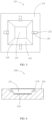
- FIG. 1 is a three-dimensional schematic diagram of a light source system 100 provided by a first embodiment of the present disclosure
- FIG. 2 is a cross-sectional view of the light source system 100 shown in FIG. 1 taken along a line II-II
- FIG. 3 is a top view of the light source system shown 100 shown in FIG. 2 .
- the light source system 100 provided by the embodiment of the present disclosure includes a substrate 110, a light guiding element 120, a laser 130, a beam deflecting device 140, a wavelength conversion layer 150, and a reflective layer 160.
- the light source system 100 in this embodiment includes at least one laser 130 configured to emit excitation light.
- the substrate 110 is made of material with a high thermal conductivity, and the material with a high thermal conductivity can be aluminum nitride, silicon nitride, silicon carbide, boron nitride, or metal such as copper or aluminum.
- the substrate 110 is provided with a notch 111, and the laser 130 is received in a sidewall of the notch 111, thereby solving a heat dissipation problem of the laser 130.
- the laser 130 and the wavelength conversion layer 150 are located in a same notch 111, and the light source system 100 and a lighting device to which the light source system 100 is applied have a small volume and a simple and compact structure.
- the beam deflecting device 140 and the laser 130 are provided in one-to-one correspondence, and the beam deflecting device 140 is configured to guide the excitation light emitted by a laser 130 corresponding the beam deflecting device 140 to be irradiated to the wavelength conversion layer 150.
- the beam deflecting device 140 can be a prism, an aspheric lens, a free arc-shaped surface, a reflective mirror, and so on.
- the reflective layer 160 can be a diffuse reflective layer or a metal reflective layer, covers a wall of the notch 111 and is configured to reflect light, to improve a light emission efficiency of the light source system 100.
- the wavelength conversion layer 150 is provided on a part of a surface of the reflective layer 160 and is configured to perform wavelength conversion on the excitation light to obtain excited light.
- the wavelength conversion layer 150 transfers heat to the substrate 110 via the reflective layer 160 and dissipates the heat through the substrate 110, thereby solving the heat dissipation problem of the wavelength conversion layer 150.
- the light guiding element 120 covers an opening of the notch 111 and is configured to reflect the excitation light and transmit the excited light, and the excited light is emitted from the light guiding element 120 to obtain light source light to be emitted by the light source system 100.
- the substrate 110 of the light source system 100 is made of material with a high thermal conductivity, and the laser 130 is received in the wall of the substrate 110.
- the heat generated by the wavelength conversion layer 150 is transferred to the substrate 110 via the reflective layer 160, thereby solving the heat dissipation problems of the laser 130 and the wavelength conversion layer 150 of the light source system.
- the light source system 100 adopts the laser 130, and the laser 130 and the wavelength conversion layer 150 are received in the notch 111 of the same substrate 110, so that the light source system 100 not only has high light emission brightness, but also has a small volume.
- the light source system 100 can also be applied to a lighting equipment, and the lighting device provided by the embodiment of the present disclosure can be applied in the fields of automobile lamp devices, stage lights, and laser headlights.
- the light source system 100 includes four identical lasers 130.
- the laser 130 can be a blue laser configured to emit blue excitation light. It can be understood that the laser 130 is not limited to the blue laser, and the laser 130 can also be an ultraviolet laser, a red laser, a green laser, or the like. It can be understood that the light source system 100 can include one or two blue lasers or a blue laser array, and the specific number of the lasers 130 of the light source system 100can be selected according to actual needs.
- the notch 111 has a shape of a frustum, and the wall of the notch 111 includes four sidewalls 111a and one bottom wall 111b.
- the laser 130 is exposed at a surface of the substrate 110, and any two lasers 130 are received in different sidewalls 111a of the notch 111.
- Each beam deflecting device 140 is disposed between the laser 130 corresponding to the beam deflecting device 140 and the light guiding element 120.
- the light source system 100 includes less than four lasers 130, for example, three lasers 130.
- Each of any three sidewalls 111a of the notch 111 can be provided with a laser 130.
- two of the three lasers 130 are disposed on one sidewall 111a and the remaining one laser 130 is disposed on another sidewall 111a.
- the three lasers 130 are all disposed on any one sidewall 111a if heat dissipation conditions allow. Due to a reflective effect of the reflective layer 160 and filtering characteristics of the light guiding element 120, the excitation light can excite the wavelength conversion layer 150 to generate the excited light, and the excited light is emitted from the light source system 100 to obtain the light source light.
- the wavelength conversion layer 150 is provided with yellow phosphors and configured to generate yellow excited light.
- the yellow excited light is emitted from the light guiding element 120 to obtain yellow light source light.
- the wavelength conversion layer 150 is provided on the reflective layer 160 at the bottom wall 111b.
- the yellow excited light emitted by the wavelength conversion layer 150 and unconverted blue excitation light are directly incident to the light guiding element 120.
- the unconverted part of the excitation light can excite the wavelength conversion layer 150 multiple times until it is converted into excited light and emitted through the light guiding element 120.
- the wavelength conversion layer 150 can be disposed on the reflective layer 160 at any position of the sidewall 111a, or any positions provided on multiple walls or a partial region of any wall of the notch 111.
- the wavelength conversion layer 150 can be configured to generate excited light of other colors under the excitation of the excitation light, such as red and green excited light. That is, the wavelength conversion layer 150 is provided with a red fluorescent material and a green fluorescent material in sections, so that optical power of the generated red excited light and that of the green excited light can reach a preset ratio. It can be understood that, in other embodiments, the wavelength conversion layer 150 can also be provided with yellow and green fluorescent materials, or yellow and red fluorescent materials, or yellow, red, and green fluorescent materials, and it is not limited to this.
- the wavelength conversion layer 150 has a rough surface, to improve the light emission efficiency of the wavelength conversion layer 150 and reduce reflection loss when the excitation light glides at a large angle.
- the reflective layer 160 is disposed on the wall, that is, the reflective layer 160 covers four sidewalls 111a and one bottom wall 111b, so as to reflect the light therein from various directions in the light source system 100, thereby increasing the number of the light reflection and improving a conversion efficiency of the excitation light.
- the light in the notch 111 can only be emitted from the light guiding element 120, which ensures the light emission efficiency of the light source system 100.
- the light guiding element 120 is configured to reflect the excitation light and transmit the excited light, and the light guiding element 120 can be a beam-splitting filter plated with a blue-reflective and yellow-transmissive film. It can be understood that in an embodiment, the light guiding element 120 is a prism provided with an optical film, and the prism facilitates multiple reflections of the excitation light in the light source system 100. In other embodiments, the light guiding element 120 can be coated according to the colors of the excitation light and the excited light.
- the notch 111 can have a shape with which its opening and the bottom wall 111b have different areas.
- an area of the bottom wall 111b is smaller than the area of the opening, such as a circular frustum shape, a circular cone shape, a pyramid shape, or other irregular shapes such as a shape having a U-shaped or V-shaped cross-section, in order to ensure that the unconverted part of the excitation light emitted from the wavelength conversion layer 150 is incident to the light guiding element 120, then the excitation light is reflected, and it is reflected by the reflective layer 160 to the wavelength conversion layer 150 and converted into excited light, which is then emitted from the light guiding element 120, so that it is also ensured that the excitation light that is not irradiated to the wavelength conversion layer 150 is guided to the wavelength conversion layer 150 through the reflective layer 160 and the light guiding element 120 to be converted into excited light, which is finally emitted from the light guiding element 120.
- the wavelength conversion layer 150 is disposed on the bottom wall of the U-shaped notch.
- FIG. 4 is a cross-sectional view of a light source system 200 provided by a second embodiment of the present disclosure
- FIG. 5 is a top view of the light source system 200 shown in FIG. 4
- FIG. 6 is a schematic diagram of spots on a wavelength conversion layer 250 shown in FIG. 4 .
- the cross-sectional view of the light source system 200 provided in the embodiment as shown in FIG. 4 is obtained in the same manner as the light source system 100.
- a difference between the light source system 200 and the light source system 100 mainly lies in: the laser 230 in the light source system 200 is received in the sidewall 211a of the notch 211 of the substrate 210 at a preset angle, in such a manner that the excitation light emitted by the laser 230 propagates along a straight line to be irradiated to the wavelength conversion layer 250, and the beam deflecting device is omitted.
- specific solutions applicable to the first embodiment can also be correspondingly applied to the second embodiment and will not be repeated herein to save space and avoid duplication.
- the laser 230 is at a certain angle with respect to the bottom wall 211b in a perpendicular direction, in such a manner that the excitation light emitted by the laser 230 propagates along a straight line to be irradiated to the wavelength conversion layer 250, thereby omitting the beam deflecting device; as shown in FIG. 4 and FIG. 5 , the laser 230 is at a certain angle with respect to the bottom wall 211b in a perpendicular direction, in such a manner that the excitation light emitted by the laser 230 propagates along a straight line to be irradiated to the wavelength conversion layer 250, thereby omitting the beam deflecting device; as shown in FIG.
- the laser 230 is at a certain angle with respect to the sidewall 211a in a horizontal direction, in such a manner that spots formed on the wavelength conversion layer 250 by any two lasers 130 partially overlap and partially do not overlap, and then spots emitted by the lasers 230 can be more uniformly irradiated on the wavelength conversion layer 250, which can avoid a problem that a conversion efficiency of the wavelength conversion layer 250 is reduced due to excessive local heat of the wavelength conversion layer 250.
- the laser spots irradiated on the wavelength conversion layer 250 are as shown in FIG. 6 .
- the light source system 200 provided in the second embodiment can solve the heat dissipation problems of the laser 230 and the wavelength conversion layer 250, and the light source system 200 and a lighting device to which the light source system 200 is applied have a small volume and a simple and compact structure. In addition, the number of optical devices used in the light source system 200 is reduced, an internal space of the light source system 200 is saved, and the cost is lower.
- FIG. 7 is a cross-sectional view of a light source system 100 provided by a third embodiment of the present disclosure as shown in FIG. 1 .
- the cross-sectional view of the light source system 300 provided in the embodiment as shown in FIG. 7 is obtained in the same manner as the light source system 100.
- a difference between the light source system 300 and the light source system 100 mainly lies in: the laser 330 of the light source system 300 emits excitation light in a first polarization state, the wavelength conversion layer 350 changes a polarization state of the excitation light, the light guiding element 320 is a polarizing prism plated with an optical film, the polarizing prism is configured to reflect light of the first polarization state and transmit light of another polarization state, that is, the polarization state of the excitation light of the first polarization state is changed by the wavelength conversion layer 350, and the excitation light of the first polarization state is finally emitted from the light guiding element 320 in forms of other polarization states, excited light of other polarization states is also emitted from the light guiding element 320, and blue excitation light and yellow excited light that are emitted from the light guiding element 320 are combined to obtain white light source light.
- the first embodiment can also be correspondingly applied to the second embodiment and will not be
- the light source system 300 provided in the third embodiment can solve the heat dissipation problems of the laser 330 and the wavelength conversion layer 350 of the light source system 300, and the light source system 300 and a lighting device to which the light source system 300 is applied have a small volume and a simple and compact structure.
Landscapes
- Physics & Mathematics (AREA)
- General Physics & Mathematics (AREA)
- Optics & Photonics (AREA)
- Engineering & Computer Science (AREA)
- General Engineering & Computer Science (AREA)
- Spectroscopy & Molecular Physics (AREA)
- Condensed Matter Physics & Semiconductors (AREA)
- Electromagnetism (AREA)
- Semiconductor Lasers (AREA)
- Non-Portable Lighting Devices Or Systems Thereof (AREA)
Claims (10)
- Lichtquellensystem (100, 200, 300), umfassend:mindestens zwei Laser (130, 230, 330), die konfiguriert sind, um Anregungslicht zu emittieren;ein Substrat (110, 210) aus einem Material mit hoher Wärmeleitfähigkeit, wobei das Substrat (110, 210) mit einer Kerbe (111, 211) versehen ist, eine Wand (111a, 211a, 111b, 211b) der Kerbe (111, 211) eine Bodenwand (111b, 211b) und Seitenwände (111a, 211a) umfasst und die mindestens zwei Laser (130, 230, 330) in verschiedenen Seitenwänden (111a, 211a) aufgenommen sind;eine reflektierende Schicht (160, 360), die die Wand (111a, 211a, 111b, 211b) der Kerbe (111, 211) bedeckt und konfiguriert ist, um das Anregungslicht zu reflektieren;eine Wellenlängenumwandlungsschicht (150, 250, 350), die auf einer Fläche der reflektierenden Schicht (160, 360), die die Bodenwand (111b, 211b) bedeckt, vorgesehen ist und konfiguriert ist, um eine Wellenlängenumwandlung des Anregungslichts durchzuführen, um angeregtes Licht zu erhalten; undein Lichtführungselement (120, 320), das eine Öffnung der Kerbe (111, 211) bedeckt und konfiguriert ist, um das Anregungslicht zu reflektieren und das angeregte Licht zu übertragen, um Licht zu erhalten, das durch das Lichtquellensystem (100, 200, 300) zu emittieren ist.
- Lichtquellensystem (100, 200, 300) nach Anspruch 1, wobei das Lichtführungselement (120, 320) einen Strahlteilungsfilter umfasst.
- Lichtquellensystem (100, 200, 300) nach Anspruch 1, wobei die Bodenwand (111b, 211b) eine sich von der Öffnung unterscheidende Fläche aufweist.
- Lichtquellensystem (100, 200, 300) nach Anspruch 1, ferner umfassend:
mindestens zwei Strahlbeugungsvorrichtungen (140) in Eins-zu-eins-Entsprechung mit den mindestens zwei Lasern (130, 230, 330), wobei jede der mindestens zwei Strahlbeugungsvorrichtungen (140) konfiguriert ist, um Anregungslicht, das von einem entsprechenden der mindestens zwei Laser (130, 230, 330) emittiert wird, so zu führen, dass es die Wellenlängenumwandlungsschicht (150, 250, 350) bestrahlt. - Lichtquellensystem (100, 200, 300) nach Anspruch 4, wobei die Kerbe (111, 211) eine Form eines Kegelstumpfes aufweist, die mindestens zwei Laser (130, 230, 330) von einer Fläche des Substrats (110, 210) freiliegen, die zwei Laser (130, 230, 330) in verschiedenen Seitenwänden der Kerbe (111, 211) aufgenommen sind und jede der mindestens zwei Strahlbeugungsvorrichtungen (140) zwischen dem entsprechenden der mindestens zwei Laser (130, 230, 330) und dem Lichtführungselement (120, 320) angeordnet ist.
- Lichtquellensystem (100, 200, 300) nach Anspruch 1, wobei die mindestens zwei Laser (130, 230, 330) eine Vielzahl von Lasern umfassen und jeder der Vielzahl von Lasern in einer der Seitenwände (111a, 211a) der Kerbe (111, 211) in einem vorgegebenen Winkel derart aufgenommen ist, dass sich das von dem Laser emittierte Anregungslicht in einer geraden Linie ausbreitet, um die Wellenlängenumwandlungsschicht (150, 250, 350) zu bestrahlen.
- Lichtquellensystem (100, 200, 300) nach Anspruch 5, wobei sich Stellen, die auf der Wellenlängenumwandlungsschicht (150, 250, 350) durch verschiedene Laser der mindestens zwei Laser (130, 230, 330) ausgebildet sind, teilweise überlappen.
- Lichtquellensystem (100, 200, 300) nach Anspruch 1, wobei das Lichtführungselement (120, 320) ein Prisma ist.
- Lichtquellensystem (100, 200, 300) nach Anspruch 8, wobei die mindestens zwei Laser (130, 230, 330) Anregungslicht in einem ersten Polarisationszustand emittieren, die Wellenlängenumwandlungsschicht (150, 250, 350) so konfiguriert ist, dass sie den Polarisationszustand des Anregungslichts ändert, und das Lichtführungselement (120, 320) so konfiguriert ist, dass es Licht des ersten Polarisationszustands reflektiert und Licht eines anderen Polarisationszustands überträgt.
- Beleuchtungsvorrichtung, umfassend das Lichtquellensystem (100, 200, 300) nach einem der Ansprüche 1-9.
Applications Claiming Priority (2)
| Application Number | Priority Date | Filing Date | Title |
|---|---|---|---|
| CN201711466234 | 2017-12-28 | ||
| PCT/CN2018/088524 WO2019128079A1 (zh) | 2017-12-28 | 2018-05-25 | 光源系统及照明装置 |
Publications (3)
| Publication Number | Publication Date |
|---|---|
| EP3734673A1 EP3734673A1 (de) | 2020-11-04 |
| EP3734673A4 EP3734673A4 (de) | 2021-11-24 |
| EP3734673B1 true EP3734673B1 (de) | 2025-04-16 |
Family
ID=67065001
Family Applications (1)
| Application Number | Title | Priority Date | Filing Date |
|---|---|---|---|
| EP18895195.8A Active EP3734673B1 (de) | 2017-12-28 | 2018-05-25 | Lichtquellensystem und beleuchtungsvorrichtung |
Country Status (3)
| Country | Link |
|---|---|
| US (1) | US11098886B2 (de) |
| EP (1) | EP3734673B1 (de) |
| WO (1) | WO2019128079A1 (de) |
Families Citing this family (5)
| Publication number | Priority date | Publication date | Assignee | Title |
|---|---|---|---|---|
| CN112240493A (zh) * | 2019-07-16 | 2021-01-19 | 深圳市绎立锐光科技开发有限公司 | 光源系统及照明装置 |
| CN113534587B (zh) * | 2020-04-21 | 2022-08-12 | 青岛海信激光显示股份有限公司 | 激光器和投影设备 |
| EP4409196B1 (de) | 2021-10-01 | 2025-04-23 | Signify Holding B.V. | Abstimmbares laserquellen-weisslichtmodul |
| DE102022100799A1 (de) * | 2022-01-14 | 2023-07-20 | HELLA GmbH & Co. KGaA | Beleuchtungsvorrichtung für ein Kraftfahrzeug |
| EP4544218A1 (de) | 2022-06-23 | 2025-04-30 | Signify Holding B.V. | Lichtwellenleiter-spinnenmodul für laserquelle |
Family Cites Families (8)
| Publication number | Priority date | Publication date | Assignee | Title |
|---|---|---|---|---|
| CN100492685C (zh) * | 2003-12-05 | 2009-05-27 | 三菱电机株式会社 | 发光装置及利用该发光装置的照明器具 |
| AU2010279305A1 (en) * | 2009-08-07 | 2012-03-01 | Perry Felix | Method and apparatus for surface and subsurface sanitizing of food products in a cooking appliance using ultraviolet light |
| WO2011107896A1 (en) * | 2010-03-01 | 2011-09-09 | Koninklijke Philips Electronics N.V. | Lighting apparatus |
| JP5968682B2 (ja) * | 2012-05-24 | 2016-08-10 | シャープ株式会社 | 投光装置および車両用前照灯 |
| JP2014175096A (ja) | 2013-03-06 | 2014-09-22 | Toshiba Lighting & Technology Corp | 照明装置 |
| KR102114607B1 (ko) * | 2013-04-01 | 2020-05-25 | 엘지전자 주식회사 | 레이저 광원장치 |
| WO2017077757A1 (ja) * | 2015-11-06 | 2017-05-11 | シャープ株式会社 | 発光装置 |
| US10771155B2 (en) * | 2017-09-28 | 2020-09-08 | Soraa Laser Diode, Inc. | Intelligent visible light with a gallium and nitrogen containing laser source |
-
2018
- 2018-05-25 EP EP18895195.8A patent/EP3734673B1/de active Active
- 2018-05-25 WO PCT/CN2018/088524 patent/WO2019128079A1/zh not_active Ceased
- 2018-05-25 US US16/958,342 patent/US11098886B2/en active Active
Also Published As
| Publication number | Publication date |
|---|---|
| US20200400299A1 (en) | 2020-12-24 |
| US11098886B2 (en) | 2021-08-24 |
| EP3734673A1 (de) | 2020-11-04 |
| EP3734673A4 (de) | 2021-11-24 |
| WO2019128079A1 (zh) | 2019-07-04 |
Similar Documents
| Publication | Publication Date | Title |
|---|---|---|
| JP5380498B2 (ja) | 光源装置、照明装置、車両用前照灯および車両 | |
| US11098886B2 (en) | Light source system and lighting device | |
| KR101166664B1 (ko) | 고성능 발광 다이오드 램프 시스템 | |
| EP3229072B1 (de) | Beleuchtungssystem und projektionsvorrichtung | |
| CN100521266C (zh) | Led灯系统 | |
| JP2013546142A (ja) | 導光路およびフォトルミネッセンス材料を備える固体ランプ | |
| US9599300B2 (en) | Light emitting device and lighting device | |
| US20220333757A1 (en) | Hybrid led/laser light source for smart headlight applications | |
| JP2013519185A (ja) | 蛍光体、励起光源、光学システム、およびヒートシンクを備えた照明器具 | |
| JP6271216B2 (ja) | 発光ユニットおよび照明装置 | |
| US10347801B2 (en) | Light emitting device | |
| JPWO2014073136A1 (ja) | 光源および画像投写装置 | |
| CN1781053A (zh) | 光源 | |
| JP6067629B2 (ja) | 発光装置、照明装置および車両用前照灯 | |
| JP2012243701A (ja) | 光源装置および照明装置 | |
| JP2018041723A (ja) | 発光モジュールおよび車両用前照灯 | |
| CN101641801B (zh) | 用于产生混合光的装置和方法 | |
| JP2011181713A (ja) | Led光源装置及び積層型led光源装置 | |
| CN105258076A (zh) | 波长转换装置、发光装置和灯具 | |
| JP2014017052A (ja) | 光源装置およびそれを備えた投光装置 | |
| JP6072447B2 (ja) | 照明装置及び車両用前照灯 | |
| CN109424943B (zh) | 波长转换装置和激光荧光转换型光源 | |
| JP2017228390A (ja) | 照明装置 | |
| CN222774729U (zh) | 一种光源装置及照明系统与投影系统 | |
| JP2007258466A (ja) | 照明装置及び発光装置 |
Legal Events
| Date | Code | Title | Description |
|---|---|---|---|
| STAA | Information on the status of an ep patent application or granted ep patent |
Free format text: STATUS: THE INTERNATIONAL PUBLICATION HAS BEEN MADE |
|
| PUAI | Public reference made under article 153(3) epc to a published international application that has entered the european phase |
Free format text: ORIGINAL CODE: 0009012 |
|
| STAA | Information on the status of an ep patent application or granted ep patent |
Free format text: STATUS: REQUEST FOR EXAMINATION WAS MADE |
|
| 17P | Request for examination filed |
Effective date: 20200728 |
|
| AK | Designated contracting states |
Kind code of ref document: A1 Designated state(s): AL AT BE BG CH CY CZ DE DK EE ES FI FR GB GR HR HU IE IS IT LI LT LU LV MC MK MT NL NO PL PT RO RS SE SI SK SM TR |
|
| AX | Request for extension of the european patent |
Extension state: BA ME |
|
| DAV | Request for validation of the european patent (deleted) | ||
| DAX | Request for extension of the european patent (deleted) | ||
| REG | Reference to a national code |
Ipc: H01S0005000000 Ref country code: DE Ref legal event code: R079 Ref document number: 602018081218 Country of ref document: DE Free format text: PREVIOUS MAIN CLASS: H01L0033000000 Ipc: H01S0005000000 |
|
| A4 | Supplementary search report drawn up and despatched |
Effective date: 20211021 |
|
| RIC1 | Information provided on ipc code assigned before grant |
Ipc: F21V 9/30 20180101ALI20211015BHEP Ipc: F21S 41/20 20180101ALI20211015BHEP Ipc: F21S 41/176 20180101ALI20211015BHEP Ipc: F21S 41/16 20180101ALI20211015BHEP Ipc: H01S 5/00 20060101AFI20211015BHEP |
|
| GRAP | Despatch of communication of intention to grant a patent |
Free format text: ORIGINAL CODE: EPIDOSNIGR1 |
|
| STAA | Information on the status of an ep patent application or granted ep patent |
Free format text: STATUS: GRANT OF PATENT IS INTENDED |
|
| INTG | Intention to grant announced |
Effective date: 20241118 |
|
| GRAS | Grant fee paid |
Free format text: ORIGINAL CODE: EPIDOSNIGR3 |
|
| GRAA | (expected) grant |
Free format text: ORIGINAL CODE: 0009210 |
|
| STAA | Information on the status of an ep patent application or granted ep patent |
Free format text: STATUS: THE PATENT HAS BEEN GRANTED |
|
| AK | Designated contracting states |
Kind code of ref document: B1 Designated state(s): AL AT BE BG CH CY CZ DE DK EE ES FI FR GB GR HR HU IE IS IT LI LT LU LV MC MK MT NL NO PL PT RO RS SE SI SK SM TR |
|
| REG | Reference to a national code |
Ref country code: GB Ref legal event code: FG4D |
|
| REG | Reference to a national code |
Ref country code: CH Ref legal event code: EP Ref country code: DE Ref legal event code: R096 Ref document number: 602018081218 Country of ref document: DE |
|
| REG | Reference to a national code |
Ref country code: IE Ref legal event code: FG4D |
|
| PGFP | Annual fee paid to national office [announced via postgrant information from national office to epo] |
Ref country code: DE Payment date: 20250513 Year of fee payment: 8 |
|
| PGFP | Annual fee paid to national office [announced via postgrant information from national office to epo] |
Ref country code: GB Payment date: 20250521 Year of fee payment: 8 |
|
| PGFP | Annual fee paid to national office [announced via postgrant information from national office to epo] |
Ref country code: FR Payment date: 20250530 Year of fee payment: 8 |
|
| REG | Reference to a national code |
Ref country code: NL Ref legal event code: MP Effective date: 20250416 |
|
| PG25 | Lapsed in a contracting state [announced via postgrant information from national office to epo] |
Ref country code: NL Free format text: LAPSE BECAUSE OF FAILURE TO SUBMIT A TRANSLATION OF THE DESCRIPTION OR TO PAY THE FEE WITHIN THE PRESCRIBED TIME-LIMIT Effective date: 20250416 |
|
| REG | Reference to a national code |
Ref country code: AT Ref legal event code: MK05 Ref document number: 1786466 Country of ref document: AT Kind code of ref document: T Effective date: 20250416 |
|
| PG25 | Lapsed in a contracting state [announced via postgrant information from national office to epo] |
Ref country code: FI Free format text: LAPSE BECAUSE OF FAILURE TO SUBMIT A TRANSLATION OF THE DESCRIPTION OR TO PAY THE FEE WITHIN THE PRESCRIBED TIME-LIMIT Effective date: 20250416 Ref country code: PT Free format text: LAPSE BECAUSE OF FAILURE TO SUBMIT A TRANSLATION OF THE DESCRIPTION OR TO PAY THE FEE WITHIN THE PRESCRIBED TIME-LIMIT Effective date: 20250818 Ref country code: ES Free format text: LAPSE BECAUSE OF FAILURE TO SUBMIT A TRANSLATION OF THE DESCRIPTION OR TO PAY THE FEE WITHIN THE PRESCRIBED TIME-LIMIT Effective date: 20250416 |
|
| REG | Reference to a national code |
Ref country code: LT Ref legal event code: MG9D |
|
| PG25 | Lapsed in a contracting state [announced via postgrant information from national office to epo] |
Ref country code: GR Free format text: LAPSE BECAUSE OF FAILURE TO SUBMIT A TRANSLATION OF THE DESCRIPTION OR TO PAY THE FEE WITHIN THE PRESCRIBED TIME-LIMIT Effective date: 20250717 Ref country code: NO Free format text: LAPSE BECAUSE OF FAILURE TO SUBMIT A TRANSLATION OF THE DESCRIPTION OR TO PAY THE FEE WITHIN THE PRESCRIBED TIME-LIMIT Effective date: 20250716 |
|
| PG25 | Lapsed in a contracting state [announced via postgrant information from national office to epo] |
Ref country code: PL Free format text: LAPSE BECAUSE OF FAILURE TO SUBMIT A TRANSLATION OF THE DESCRIPTION OR TO PAY THE FEE WITHIN THE PRESCRIBED TIME-LIMIT Effective date: 20250416 |
|
| PG25 | Lapsed in a contracting state [announced via postgrant information from national office to epo] |
Ref country code: BG Free format text: LAPSE BECAUSE OF FAILURE TO SUBMIT A TRANSLATION OF THE DESCRIPTION OR TO PAY THE FEE WITHIN THE PRESCRIBED TIME-LIMIT Effective date: 20250416 |
|
| PG25 | Lapsed in a contracting state [announced via postgrant information from national office to epo] |
Ref country code: HR Free format text: LAPSE BECAUSE OF FAILURE TO SUBMIT A TRANSLATION OF THE DESCRIPTION OR TO PAY THE FEE WITHIN THE PRESCRIBED TIME-LIMIT Effective date: 20250416 |
|
| PG25 | Lapsed in a contracting state [announced via postgrant information from national office to epo] |
Ref country code: AT Free format text: LAPSE BECAUSE OF FAILURE TO SUBMIT A TRANSLATION OF THE DESCRIPTION OR TO PAY THE FEE WITHIN THE PRESCRIBED TIME-LIMIT Effective date: 20250416 |
|
| PG25 | Lapsed in a contracting state [announced via postgrant information from national office to epo] |
Ref country code: RS Free format text: LAPSE BECAUSE OF FAILURE TO SUBMIT A TRANSLATION OF THE DESCRIPTION OR TO PAY THE FEE WITHIN THE PRESCRIBED TIME-LIMIT Effective date: 20250716 |
|
| PG25 | Lapsed in a contracting state [announced via postgrant information from national office to epo] |
Ref country code: IS Free format text: LAPSE BECAUSE OF FAILURE TO SUBMIT A TRANSLATION OF THE DESCRIPTION OR TO PAY THE FEE WITHIN THE PRESCRIBED TIME-LIMIT Effective date: 20250816 |
|
| PG25 | Lapsed in a contracting state [announced via postgrant information from national office to epo] |
Ref country code: LV Free format text: LAPSE BECAUSE OF FAILURE TO SUBMIT A TRANSLATION OF THE DESCRIPTION OR TO PAY THE FEE WITHIN THE PRESCRIBED TIME-LIMIT Effective date: 20250416 |
|
| REG | Reference to a national code |
Ref country code: CH Ref legal event code: H13 Free format text: ST27 STATUS EVENT CODE: U-0-0-H10-H13 (AS PROVIDED BY THE NATIONAL OFFICE) Effective date: 20251223 |
|
| PG25 | Lapsed in a contracting state [announced via postgrant information from national office to epo] |
Ref country code: SM Free format text: LAPSE BECAUSE OF FAILURE TO SUBMIT A TRANSLATION OF THE DESCRIPTION OR TO PAY THE FEE WITHIN THE PRESCRIBED TIME-LIMIT Effective date: 20250416 Ref country code: DK Free format text: LAPSE BECAUSE OF FAILURE TO SUBMIT A TRANSLATION OF THE DESCRIPTION OR TO PAY THE FEE WITHIN THE PRESCRIBED TIME-LIMIT Effective date: 20250416 |
|
| PG25 | Lapsed in a contracting state [announced via postgrant information from national office to epo] |
Ref country code: LU Free format text: LAPSE BECAUSE OF NON-PAYMENT OF DUE FEES Effective date: 20250525 |
|
| PG25 | Lapsed in a contracting state [announced via postgrant information from national office to epo] |
Ref country code: CH Free format text: LAPSE BECAUSE OF NON-PAYMENT OF DUE FEES Effective date: 20250531 |
|
| REG | Reference to a national code |
Ref country code: DE Ref legal event code: R097 Ref document number: 602018081218 Country of ref document: DE |
|
| PG25 | Lapsed in a contracting state [announced via postgrant information from national office to epo] |
Ref country code: CZ Free format text: LAPSE BECAUSE OF FAILURE TO SUBMIT A TRANSLATION OF THE DESCRIPTION OR TO PAY THE FEE WITHIN THE PRESCRIBED TIME-LIMIT Effective date: 20250416 |
|
| PG25 | Lapsed in a contracting state [announced via postgrant information from national office to epo] |
Ref country code: EE Free format text: LAPSE BECAUSE OF FAILURE TO SUBMIT A TRANSLATION OF THE DESCRIPTION OR TO PAY THE FEE WITHIN THE PRESCRIBED TIME-LIMIT Effective date: 20250416 |
|
| PG25 | Lapsed in a contracting state [announced via postgrant information from national office to epo] |
Ref country code: RO Free format text: LAPSE BECAUSE OF FAILURE TO SUBMIT A TRANSLATION OF THE DESCRIPTION OR TO PAY THE FEE WITHIN THE PRESCRIBED TIME-LIMIT Effective date: 20250416 Ref country code: SK Free format text: LAPSE BECAUSE OF FAILURE TO SUBMIT A TRANSLATION OF THE DESCRIPTION OR TO PAY THE FEE WITHIN THE PRESCRIBED TIME-LIMIT Effective date: 20250416 |
|
| PG25 | Lapsed in a contracting state [announced via postgrant information from national office to epo] |
Ref country code: IT Free format text: LAPSE BECAUSE OF FAILURE TO SUBMIT A TRANSLATION OF THE DESCRIPTION OR TO PAY THE FEE WITHIN THE PRESCRIBED TIME-LIMIT Effective date: 20250416 |
|
| REG | Reference to a national code |
Ref country code: BE Ref legal event code: MM Effective date: 20250531 |
|
| PG25 | Lapsed in a contracting state [announced via postgrant information from national office to epo] |
Ref country code: MC Free format text: LAPSE BECAUSE OF FAILURE TO SUBMIT A TRANSLATION OF THE DESCRIPTION OR TO PAY THE FEE WITHIN THE PRESCRIBED TIME-LIMIT Effective date: 20250416 |
|
| PLBE | No opposition filed within time limit |
Free format text: ORIGINAL CODE: 0009261 |
|
| STAA | Information on the status of an ep patent application or granted ep patent |
Free format text: STATUS: NO OPPOSITION FILED WITHIN TIME LIMIT |
|
| REG | Reference to a national code |
Ref country code: CH Ref legal event code: L10 Free format text: ST27 STATUS EVENT CODE: U-0-0-L10-L00 (AS PROVIDED BY THE NATIONAL OFFICE) Effective date: 20260225 |
|
| 26N | No opposition filed |
Effective date: 20260119 |
|
| PG25 | Lapsed in a contracting state [announced via postgrant information from national office to epo] |
Ref country code: IE Free format text: LAPSE BECAUSE OF NON-PAYMENT OF DUE FEES Effective date: 20250525 |
|
| PG25 | Lapsed in a contracting state [announced via postgrant information from national office to epo] |
Ref country code: BE Free format text: LAPSE BECAUSE OF NON-PAYMENT OF DUE FEES Effective date: 20250531 |