EP3734657B1 - Halbleitergehäuse - Google Patents
Halbleitergehäuse Download PDFInfo
- Publication number
- EP3734657B1 EP3734657B1 EP20167443.9A EP20167443A EP3734657B1 EP 3734657 B1 EP3734657 B1 EP 3734657B1 EP 20167443 A EP20167443 A EP 20167443A EP 3734657 B1 EP3734657 B1 EP 3734657B1
- Authority
- EP
- European Patent Office
- Prior art keywords
- semiconductor chip
- disposed
- connection member
- layer
- connection
- Prior art date
- Legal status (The legal status is an assumption and is not a legal conclusion. Google has not performed a legal analysis and makes no representation as to the accuracy of the status listed.)
- Active
Links
Images






Classifications
-
- H—ELECTRICITY
- H10—SEMICONDUCTOR DEVICES; ELECTRIC SOLID-STATE DEVICES NOT OTHERWISE PROVIDED FOR
- H10W—GENERIC PACKAGES, INTERCONNECTIONS, CONNECTORS OR OTHER CONSTRUCTIONAL DETAILS OF DEVICES COVERED BY CLASS H10
- H10W70/00—Package substrates; Interposers; Redistribution layers [RDL]
- H10W70/60—Insulating or insulated package substrates; Interposers; Redistribution layers
- H10W70/611—Insulating or insulated package substrates; Interposers; Redistribution layers for connecting multiple chips together
- H10W70/614—Insulating or insulated package substrates; Interposers; Redistribution layers for connecting multiple chips together the multiple chips being integrally enclosed
-
- H—ELECTRICITY
- H10—SEMICONDUCTOR DEVICES; ELECTRIC SOLID-STATE DEVICES NOT OTHERWISE PROVIDED FOR
- H10W—GENERIC PACKAGES, INTERCONNECTIONS, CONNECTORS OR OTHER CONSTRUCTIONAL DETAILS OF DEVICES COVERED BY CLASS H10
- H10W20/00—Interconnections in chips, wafers or substrates
- H10W20/20—Interconnections within wafers or substrates, e.g. through-silicon vias [TSV]
-
- H—ELECTRICITY
- H10—SEMICONDUCTOR DEVICES; ELECTRIC SOLID-STATE DEVICES NOT OTHERWISE PROVIDED FOR
- H10W—GENERIC PACKAGES, INTERCONNECTIONS, CONNECTORS OR OTHER CONSTRUCTIONAL DETAILS OF DEVICES COVERED BY CLASS H10
- H10W70/00—Package substrates; Interposers; Redistribution layers [RDL]
- H10W70/01—Manufacture or treatment
- H10W70/05—Manufacture or treatment of insulating or insulated package substrates, or of interposers, or of redistribution layers
- H10W70/08—Manufacture or treatment of insulating or insulated package substrates, or of interposers, or of redistribution layers by depositing layers on the chip or wafer, e.g. "chip-first" RDLs
- H10W70/09—Manufacture or treatment of insulating or insulated package substrates, or of interposers, or of redistribution layers by depositing layers on the chip or wafer, e.g. "chip-first" RDLs extending onto an encapsulation that laterally surrounds the chip or wafer, e.g. fan-out wafer level package [FOWLP] RDLs
-
- H—ELECTRICITY
- H10—SEMICONDUCTOR DEVICES; ELECTRIC SOLID-STATE DEVICES NOT OTHERWISE PROVIDED FOR
- H10W—GENERIC PACKAGES, INTERCONNECTIONS, CONNECTORS OR OTHER CONSTRUCTIONAL DETAILS OF DEVICES COVERED BY CLASS H10
- H10W72/00—Interconnections or connectors in packages
-
- H—ELECTRICITY
- H10—SEMICONDUCTOR DEVICES; ELECTRIC SOLID-STATE DEVICES NOT OTHERWISE PROVIDED FOR
- H10W—GENERIC PACKAGES, INTERCONNECTIONS, CONNECTORS OR OTHER CONSTRUCTIONAL DETAILS OF DEVICES COVERED BY CLASS H10
- H10W72/00—Interconnections or connectors in packages
- H10W72/20—Bump connectors, e.g. solder bumps or copper pillars; Dummy bumps; Thermal bumps
-
- H—ELECTRICITY
- H10—SEMICONDUCTOR DEVICES; ELECTRIC SOLID-STATE DEVICES NOT OTHERWISE PROVIDED FOR
- H10W—GENERIC PACKAGES, INTERCONNECTIONS, CONNECTORS OR OTHER CONSTRUCTIONAL DETAILS OF DEVICES COVERED BY CLASS H10
- H10W72/00—Interconnections or connectors in packages
- H10W72/90—Bond pads, in general
-
- H—ELECTRICITY
- H10—SEMICONDUCTOR DEVICES; ELECTRIC SOLID-STATE DEVICES NOT OTHERWISE PROVIDED FOR
- H10W—GENERIC PACKAGES, INTERCONNECTIONS, CONNECTORS OR OTHER CONSTRUCTIONAL DETAILS OF DEVICES COVERED BY CLASS H10
- H10W74/00—Encapsulations, e.g. protective coatings
- H10W74/10—Encapsulations, e.g. protective coatings characterised by their shape or disposition
- H10W74/111—Encapsulations, e.g. protective coatings characterised by their shape or disposition the semiconductor body being completely enclosed
- H10W74/114—Encapsulations, e.g. protective coatings characterised by their shape or disposition the semiconductor body being completely enclosed by a substrate and the encapsulations
-
- H—ELECTRICITY
- H10—SEMICONDUCTOR DEVICES; ELECTRIC SOLID-STATE DEVICES NOT OTHERWISE PROVIDED FOR
- H10W—GENERIC PACKAGES, INTERCONNECTIONS, CONNECTORS OR OTHER CONSTRUCTIONAL DETAILS OF DEVICES COVERED BY CLASS H10
- H10W74/00—Encapsulations, e.g. protective coatings
- H10W74/10—Encapsulations, e.g. protective coatings characterised by their shape or disposition
- H10W74/111—Encapsulations, e.g. protective coatings characterised by their shape or disposition the semiconductor body being completely enclosed
- H10W74/114—Encapsulations, e.g. protective coatings characterised by their shape or disposition the semiconductor body being completely enclosed by a substrate and the encapsulations
- H10W74/117—Encapsulations, e.g. protective coatings characterised by their shape or disposition the semiconductor body being completely enclosed by a substrate and the encapsulations the substrate having spherical bumps for external connection
-
- H—ELECTRICITY
- H10—SEMICONDUCTOR DEVICES; ELECTRIC SOLID-STATE DEVICES NOT OTHERWISE PROVIDED FOR
- H10W—GENERIC PACKAGES, INTERCONNECTIONS, CONNECTORS OR OTHER CONSTRUCTIONAL DETAILS OF DEVICES COVERED BY CLASS H10
- H10W90/00—Package configurations
-
- H—ELECTRICITY
- H10—SEMICONDUCTOR DEVICES; ELECTRIC SOLID-STATE DEVICES NOT OTHERWISE PROVIDED FOR
- H10W—GENERIC PACKAGES, INTERCONNECTIONS, CONNECTORS OR OTHER CONSTRUCTIONAL DETAILS OF DEVICES COVERED BY CLASS H10
- H10W70/00—Package substrates; Interposers; Redistribution layers [RDL]
- H10W70/60—Insulating or insulated package substrates; Interposers; Redistribution layers
-
- H—ELECTRICITY
- H10—SEMICONDUCTOR DEVICES; ELECTRIC SOLID-STATE DEVICES NOT OTHERWISE PROVIDED FOR
- H10W—GENERIC PACKAGES, INTERCONNECTIONS, CONNECTORS OR OTHER CONSTRUCTIONAL DETAILS OF DEVICES COVERED BY CLASS H10
- H10W70/00—Package substrates; Interposers; Redistribution layers [RDL]
- H10W70/60—Insulating or insulated package substrates; Interposers; Redistribution layers
- H10W70/62—Insulating or insulated package substrates; Interposers; Redistribution layers characterised by their interconnections
- H10W70/65—Shapes or dispositions of interconnections
- H10W70/652—Cross-sectional shapes
-
- H—ELECTRICITY
- H10—SEMICONDUCTOR DEVICES; ELECTRIC SOLID-STATE DEVICES NOT OTHERWISE PROVIDED FOR
- H10W—GENERIC PACKAGES, INTERCONNECTIONS, CONNECTORS OR OTHER CONSTRUCTIONAL DETAILS OF DEVICES COVERED BY CLASS H10
- H10W70/00—Package substrates; Interposers; Redistribution layers [RDL]
- H10W70/60—Insulating or insulated package substrates; Interposers; Redistribution layers
- H10W70/62—Insulating or insulated package substrates; Interposers; Redistribution layers characterised by their interconnections
- H10W70/65—Shapes or dispositions of interconnections
- H10W70/654—Top-view layouts
- H10W70/655—Fan-out layouts
-
- H—ELECTRICITY
- H10—SEMICONDUCTOR DEVICES; ELECTRIC SOLID-STATE DEVICES NOT OTHERWISE PROVIDED FOR
- H10W—GENERIC PACKAGES, INTERCONNECTIONS, CONNECTORS OR OTHER CONSTRUCTIONAL DETAILS OF DEVICES COVERED BY CLASS H10
- H10W72/00—Interconnections or connectors in packages
- H10W72/20—Bump connectors, e.g. solder bumps or copper pillars; Dummy bumps; Thermal bumps
- H10W72/221—Structures or relative sizes
-
- H—ELECTRICITY
- H10—SEMICONDUCTOR DEVICES; ELECTRIC SOLID-STATE DEVICES NOT OTHERWISE PROVIDED FOR
- H10W—GENERIC PACKAGES, INTERCONNECTIONS, CONNECTORS OR OTHER CONSTRUCTIONAL DETAILS OF DEVICES COVERED BY CLASS H10
- H10W72/00—Interconnections or connectors in packages
- H10W72/20—Bump connectors, e.g. solder bumps or copper pillars; Dummy bumps; Thermal bumps
- H10W72/29—Bond pads specially adapted therefor
-
- H—ELECTRICITY
- H10—SEMICONDUCTOR DEVICES; ELECTRIC SOLID-STATE DEVICES NOT OTHERWISE PROVIDED FOR
- H10W—GENERIC PACKAGES, INTERCONNECTIONS, CONNECTORS OR OTHER CONSTRUCTIONAL DETAILS OF DEVICES COVERED BY CLASS H10
- H10W74/00—Encapsulations, e.g. protective coatings
- H10W74/10—Encapsulations, e.g. protective coatings characterised by their shape or disposition
- H10W74/15—Encapsulations, e.g. protective coatings characterised by their shape or disposition on active surfaces of flip-chip devices, e.g. underfills
-
- H—ELECTRICITY
- H10—SEMICONDUCTOR DEVICES; ELECTRIC SOLID-STATE DEVICES NOT OTHERWISE PROVIDED FOR
- H10W—GENERIC PACKAGES, INTERCONNECTIONS, CONNECTORS OR OTHER CONSTRUCTIONAL DETAILS OF DEVICES COVERED BY CLASS H10
- H10W90/00—Package configurations
- H10W90/20—Configurations of stacked chips
- H10W90/24—Configurations of stacked chips at least one of the stacked chips being laterally offset from a neighbouring stacked chip, e.g. chip stacks having a staircase shape
-
- H—ELECTRICITY
- H10—SEMICONDUCTOR DEVICES; ELECTRIC SOLID-STATE DEVICES NOT OTHERWISE PROVIDED FOR
- H10W—GENERIC PACKAGES, INTERCONNECTIONS, CONNECTORS OR OTHER CONSTRUCTIONAL DETAILS OF DEVICES COVERED BY CLASS H10
- H10W90/00—Package configurations
- H10W90/701—Package configurations characterised by the relative positions of pads or connectors relative to package parts
-
- H—ELECTRICITY
- H10—SEMICONDUCTOR DEVICES; ELECTRIC SOLID-STATE DEVICES NOT OTHERWISE PROVIDED FOR
- H10W—GENERIC PACKAGES, INTERCONNECTIONS, CONNECTORS OR OTHER CONSTRUCTIONAL DETAILS OF DEVICES COVERED BY CLASS H10
- H10W90/00—Package configurations
- H10W90/701—Package configurations characterised by the relative positions of pads or connectors relative to package parts
- H10W90/721—Package configurations characterised by the relative positions of pads or connectors relative to package parts of bump connectors
- H10W90/724—Package configurations characterised by the relative positions of pads or connectors relative to package parts of bump connectors between a chip and a stacked insulating package substrate, interposer or RDL
-
- H—ELECTRICITY
- H10—SEMICONDUCTOR DEVICES; ELECTRIC SOLID-STATE DEVICES NOT OTHERWISE PROVIDED FOR
- H10W—GENERIC PACKAGES, INTERCONNECTIONS, CONNECTORS OR OTHER CONSTRUCTIONAL DETAILS OF DEVICES COVERED BY CLASS H10
- H10W90/00—Package configurations
- H10W90/701—Package configurations characterised by the relative positions of pads or connectors relative to package parts
- H10W90/731—Package configurations characterised by the relative positions of pads or connectors relative to package parts of die-attach connectors
- H10W90/732—Package configurations characterised by the relative positions of pads or connectors relative to package parts of die-attach connectors between stacked chips
-
- H—ELECTRICITY
- H10—SEMICONDUCTOR DEVICES; ELECTRIC SOLID-STATE DEVICES NOT OTHERWISE PROVIDED FOR
- H10W—GENERIC PACKAGES, INTERCONNECTIONS, CONNECTORS OR OTHER CONSTRUCTIONAL DETAILS OF DEVICES COVERED BY CLASS H10
- H10W90/00—Package configurations
- H10W90/701—Package configurations characterised by the relative positions of pads or connectors relative to package parts
- H10W90/731—Package configurations characterised by the relative positions of pads or connectors relative to package parts of die-attach connectors
- H10W90/734—Package configurations characterised by the relative positions of pads or connectors relative to package parts of die-attach connectors between a chip and a stacked insulating package substrate, interposer or RDL
-
- H—ELECTRICITY
- H10—SEMICONDUCTOR DEVICES; ELECTRIC SOLID-STATE DEVICES NOT OTHERWISE PROVIDED FOR
- H10W—GENERIC PACKAGES, INTERCONNECTIONS, CONNECTORS OR OTHER CONSTRUCTIONAL DETAILS OF DEVICES COVERED BY CLASS H10
- H10W90/00—Package configurations
- H10W90/701—Package configurations characterised by the relative positions of pads or connectors relative to package parts
- H10W90/751—Package configurations characterised by the relative positions of pads or connectors relative to package parts of bond wires
- H10W90/754—Package configurations characterised by the relative positions of pads or connectors relative to package parts of bond wires between a chip and a stacked insulating package substrate, interposer or RDL
Definitions
- Example embodiments of the present disclosure relate to a semiconductor package.
- EP2916351 describes integrated circuit package assemblies in which dies are embedded in embedding substrates to provide larger pitch interconnects to facilitate coupling to substrates or circuit boards through flip chip techniques.
- the embedding substrates may contain conductive pathways for coupling die contacts to larger pitch contacts located on the embedding substrate.
- US2014/070422 describes a semiconductor device using discrete connection blocks having through vias and/or integrated passive devices formed therein are provided for PoP applications.
- the semiconductor device includes a die and a connection block encased in a molding compound. Interconnection layers are formed on surfaces of the die, the connection block and the molding compound. One or more dies and/or packages may be attached to the interconnection layers.
- US2016/365324 describes a method of manufacturing a wafer level package.
- the method includes forming a repassivation layer that encapsulates a plurality of semiconductor chips isolated from a wafer, forming a through encapsulation via (TEV) in the repassivation layer, forming a redistribution layer electrically connected to the TEV, and forming a bump ball on the redistribution layer.
- TEV through encapsulation via
- US2016/338202 describes an electronic component package including a frame having a through-hole, an electronic component disposed in the through-hole of the frame, and a redistribution part disposed at one side of the frame and the electronic component.
- KR101922885 discloses a fan-out semiconductor package includes first and second structures.
- the first structure includes a first semiconductor chip, a first encapsulant, and a connection member.
- the second structure includes a second semiconductor chip, a second encapsulant, and conductive bumps.
- the first and second structures are disposed so that active surfaces of the first and second semiconductor chips face each other.
- the conductive bumps are electrically connected to a redistribution layer, and connection pads of the first and second semiconductor chips are connected to each other through the redistribution layer in a signal manner.
- the present invention provides a semiconductor package according to the appended claims.
- Example embodiments of the present disclosure provide a semiconductor package having improved package performance and having an appropriate package size.
- An example embodiment is to provide a semiconductor chip, an application processor chip, for example, which is divided into a plurality of semiconductor chips and the plurality of semiconductor chips is stacked in a vertical direction. Further, by disposing a through-via penetrating a semiconductor chip separately disposed on a lower side and/or an electronic component embedded in the semiconductor chip disposed on the lower side and connected to the through-via in the semiconductor chip disposed on the lower side, power transfer properties, and the like, may improve.
- a semiconductor package including a package structure including a base connection member including a redistribution layer, a first semiconductor chip including a plurality of first connection pads connected to the redistribution layer, an encapsulant disposed on the base connection member and covering at least a portion of the first semiconductor chip, and a backside connection member disposed on the encapsulant and including a backside wiring layer electrically connected to the redistribution layer, a through-via (120V) connecting the redistribution layer to the backside wiring layer by penetrating through the first semiconductor chip, and an electronic component (120C) disposed inside of the first semiconductor chip and electrically connected to the through-via, and a second semiconductor chip disposed on the base connection member or the backside connection member, the second semiconductor chip including a plurality of second connection pads connected to the redistribution layer or the backside wiring layer.
- the second semiconductor chip includes a logic circuit
- the first semiconductor chip includes a logic input terminal and a logic output terminal that are respectively connected to
- the package structure may further comprise an interconnect member disposed between the base connection member and the backside connection member and electronically connecting the redistribution layer and the backside wiring layer.
- the plurality of second connection pads may comprise at least a first group of second connection pads and a second group of second connection pads, and second connection pads included in the first group are connected to the logic circuit.
- the plurality of first connection pads may comprise an input pad connected to the logic input terminal and an output pad connected to the logic output terminal.
- the logic circuit comprises a central processing unit, a graphics processing unit, a neural processing unit, a digital signal processor unit, or an image signal processing unit.
- the second semiconductor chip may overlap the first semiconductor chip in a direction in which the second semiconductor chip is disposed on the first semiconductor chip. At least a portion of the plurality of second connection pads may be electrically connected to one of the backside wiring layer and the redistribution layer through the through-via.
- the semiconductor package may comprise: a third package structure comprising a third connection member disposed on an upper side of the second semiconductor chip, a third semiconductor chip disposed on the third connection member, a molding material disposed on the third connection member and covering at least a portion of the third semiconductor chip, and a third electrical connector metal connecting the third connection member to one of the base connection member and the backside connection member.
- the third semiconductor chip may comprise a memory.
- the second semiconductor chip may further include a memory input terminal and a memory output terminal for the memory.
- the plurality of second connection pads may comprise at least a first group of the second connection pads and a second group of the second connection pads.
- the second connection pads included in the first group may be connected to the logic circuit, and second connection pads included the second group may be connected to the memory input terminal and the memory output terminal.
- the plurality of first connection pads may comprise an input pad and an output pad respectively connected to the logic input terminal and the logic output terminal.
- the semiconductor package may further comprise: a plurality of connection bumps disposed between the package structure and the second semiconductor chip and connecting the plurality of second connection pads to at least one of the redistribution layer and the backside wiring layer.
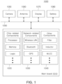
- FIG. 1 is a block diagram illustrating a block diagram illustrating an example of an electronic device system.
- an electronic device 1000 may include a mainboard 1010 therein.
- the mainboard 1010 may include chip related components 1020, network related components 1030, other components 1040, and the like, physically or electrically connected thereto. These components may be connected to others to be described below to form various signal lines 1090.
- the chip related components 1020 may include a memory chip such as a volatile memory (for example, a dynamic random access memory (DRAM)), a non-volatile memory (for example, a read only memory (ROM)), a flash memory, or the like; an application processor chip such as a central processor (for example, a central processing unit (CPU)), a graphics processor (for example, a graphics processing unit (GPU)), a digital signal processor, a cryptographic processor, a microprocessor, a microcontroller, or the like; and a logic chip such as an analog-to-digital (ADC) converter, an application-specific integrated circuit (ASIC), or the like.
- the chip related components 1020 are not limited thereto, but may also include other types of chip related components.
- the chip related components 1020 may be combined with each other.
- the network related components 1030 may include protocols such as wireless fidelity (Wi-Fi) (Institute of Electrical And Electronics Engineers (IEEE) 802.11 family, or the like), worldwide interoperability for microwave access (WiMAX) (IEEE 802.16 family, or the like), IEEE 802.20, long term evolution (LTE), evolution data only (Ev-DO), high speed packet access + (HSPA+), high speed downlink packet access + (HSDPA+), high speed uplink packet access + (HSUPA+), enhanced data GSM environment (EDGE), global system for mobile communications (GSM), global positioning system (GPS), general packet radio service (GPRS), code division multiple access (CDMA), time division multiple access (TDMA), digital enhanced cordless telecommunications (DECT), Bluetooth, 3G, 4G, and 5G protocols, and any other wireless and wired protocols, designated after the abovementioned protocols.
- Wi-Fi Institutee of Electrical And Electronics Engineers (IEEE) 802.11 family, or the like
- WiMAX worldwide interoper
- the other components 1040 may include a high frequency inductor, a ferrite inductor, a power inductor, ferrite beads, a low temperature co-fired ceramic (LTCC), an electromagnetic interference (EMI) filter, a multilayer ceramic capacitor (MLCC), or the like.
- LTCC low temperature co-fired ceramic
- EMI electromagnetic interference
- MLCC multilayer ceramic capacitor
- other components 1040 are not limited thereto, but may also include passive components used for various other purposes, or the like.
- other components 1040 may be combined with each other, together with the chip related components 1020 or the network related components 1030 described above.
- the electronic device 1000 may include other components that may or may not be physically or electrically connected to the mainboard 1010. These other components may include, for example, a camera module 1050, an antenna 1060, a display device 1070, a battery 1080, an audio codec, a video codec, a power amplifier, a compass, an accelerometer, a gyroscope, a speaker, a mass storage unit (for example, a hard disk drive), a compact disk (CD) drive, a digital versatile disk (DVD) drive, or the like.
- these other components are not limited thereto, but may also include other components used for various purposes depending on a type of electronic device 1000, or the like.
- the electronic device 1000 may be a smartphone, a personal digital assistant (PDA), a digital video camera, a digital still camera, a network system, a computer, a monitor, a tablet personal computer (PC), a laptop PC, a netbook PC, a television, a video game machine, a smartwatch, an automotive component, or the like.
- PDA personal digital assistant
- PC tablet personal computer
- netbook PC netbook PC
- television a video game machine
- smartwatch an automotive component, or the like.
- the electronic device 1000 is not limited thereto, but may be any other electronic device processing data.
- FIG. 2 is a perspective diagram illustrating an example of an electronic device.
- a semiconductor package may be used for various purposes in the various electronic devices 1000 as described above.
- a motherboard 1110 may be accommodated in a body 1101 of a smartphone 1100, and various electronic components 1120 may be physically or electrically connected to the motherboard 1110.
- other components that may or may not be physically or electrically connected to the motherboard 1110 such as a camera module 1130, may be accommodated in the body 1101.
- Some of the electronic components 1120 may be the chip related components, for example, a semiconductor package 1121, but are not limited thereto.
- the electronic device is not necessarily limited to the smartphone 1100, but may be other electronic devices as described above.
- the semiconductor chip may not serve as a finished semiconductor product itself, and may be damaged due to external physical or chemical impacts. Therefore, the semiconductor chip itself may not be used, but may be packaged and used in an electronic device, or the like, in a packaged state.
- a semiconductor packaging process is necessary because there is a difference in width between a semiconductor chip and a mainboard of an electronic device in terms of electrical connection.
- a size of a connection pad and a gap between connection pads may be smaller, whereas in a mainboard used in an electronic device, a size of a component mounting pad and a gap between component mounting pads may be greater than a scale of a semiconductor chip.
- a packaging technique which may alleviate a difference in width between circuits may be required.
- a semiconductor package manufactured by such a packaging technique may be classified as a fan-in semiconductor package and a fan-out semiconductor package depending on a structure and usage.
- FIGS. 3A and 3B are cross-sectional diagrams illustrating states before and after packaging a fan-in semiconductor package according to an example embodiment.
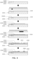
- FIG. 4 is a cross-sectional diagram illustrating a packaging process of a fan-in semiconductor package according to an example embodiment.
- a semiconductor chip 2220 may be, for example, an integrated circuit (IC) in a bare state, including a body 2221 including silicon (Si), germanium (Ge), gallium arsenide (GaAs), or the like, connection pads 2222 formed on one surface of the body 2221 and including a conductive material such as aluminum (Al), or the like, and a passivation layer 2223 such as an oxide layer, a nitride layer, or the like, formed on one surface of the body 2221 and covering at least portions of the connection pads 2222.
- the connection pads 2222 may be significantly small, it may be difficult to mount the integrated circuit (IC) on an intermediate level printed circuit board (PCB) as well as on the mainboard of the electronic device, or the like.
- a connection member 2240 may be formed depending on a size of the semiconductor chip 2220 on the semiconductor chip 2220 in order to redistribute the connection pads 2222.
- the connection member 2240 may be formed by forming an insulating layer 2241 on the semiconductor chip 2220 using an insulating material such as a photoimagable dielectric (PID) resin, forming via holes 2243h opening and exposing the connection pads 2222, and then forming wiring patterns 2242 and vias 2243. Then, a passivation layer 2250 protecting the connection member 2240 may be formed, an opening 2251 may be formed, and an underbump metal layer 2260, or the like, may be formed. That is, a fan-in semiconductor package 2200 including, for example, the semiconductor chip 2220, the connection member 2240, the passivation layer 2250, and the underbump metal layer 2260 may be manufactured through a series of processes.
- PID photoimagable dielectric
- the fan-in semiconductor package may have a package form in which all of the connection pads, for example, input/output (I/O) terminals, of the semiconductor chip are disposed inside the semiconductor chip, and may have excellent electrical characteristics and be produced at a low cost. Therefore, many elements mounted in smartphones have been manufactured in a fan-in semiconductor package form. In detail, many elements mounted in smartphones have been developed to implement a rapid signal transfer and to have a compact size.
- I/O input/output
- the fan-in semiconductor package since all I/O terminals need to be disposed inside the semiconductor chip in the fan-in semiconductor package, the fan-in semiconductor package has significant spatial limitations. Therefore, it is difficult to apply this structure to a semiconductor chip having a large number of I/O terminals or a semiconductor chip having a compact size. In addition, due to the disadvantage described above, the fan-in semiconductor package may not be directly mounted and used on the mainboard of the electronic device.
- the size of the I/O terminals of the semiconductor chip and the interval between the I/O terminals of the semiconductor chip may not be enough to directly mount the fan-in semiconductor package on the mainboard of the electronic device.
- FIG. 5 is a cross-sectional diagram illustrating an example in which a fan-in semiconductor package is mounted on a printed circuit board and mounted on a mainboard of an electronic device according to an example embodiment.
- FIG. 6 is a cross-sectional diagram illustrating an example in which a fan-in semiconductor package is mounted on a printed circuit board and mounted on a mainboard of an electronic device according to an example embodiment.
- connection pads 2222, that is, I/O terminals, of a semiconductor chip 2220 may be redistributed through a ball grid array (BGA) substrate 2301, and the fan-in semiconductor package 2200 may be ultimately mounted on a mainboard 2500 of an electronic device in a state in which it is mounted on the BGA substrate 2301.
- BGA ball grid array
- solder balls 2270, and the like may be fixed by an underfill resin 2280, or the like, and an outer side of the semiconductor chip 2220 may be covered with a molding material 2290, or the like.
- a fan-in semiconductor package 2200 may be embedded in a separate BGA substrate 2302, connection pads 2222, that is, I/O terminals, of the semiconductor chip 2220 may be redistributed by the BGA substrate 2302 in a state in which the fan-in semiconductor package 2200 is embedded in the BGA substrate 2302, and the fan-in semiconductor package 2200 may be ultimately mounted on a mainboard 2500 of an electronic device.
- the fan-in semiconductor package may be mounted on the separate BGA substrate and be then mounted on the mainboard of the electronic device through a packaging process or may be mounted and used on the mainboard of the electronic device in a state in which it is embedded in the BGA substrate.
- FIG. 7 is a cross-sectional diagram illustrating a fan-out semiconductor package according to an example embodiment.
- an outer side surfaces of a semiconductor chip 2120 may be at least partially covered by an encapsulant 2130, and connection pads 2122 of the semiconductor chip 2120 may be redistributed outwardly of the semiconductor chip 2120 by a connection member 2140.
- a passivation layer 2150 may further be formed on the connection member 2140, and an underbump metal layer 2160 may further be formed in openings of the passivation layer 2150.
- Solder balls 2170 may further be formed on the underbump metal layer 2160.
- the semiconductor chip 2120 may be an integrated circuit (IC) including a body 2121, the connection pads 2122, a passivation layer, and the like.
- the connection member 2140 may include an insulating layer 2141, redistribution layers 2142 formed on the insulating layer 2141, and vias 2143 electrically connecting the connection pads 2122 and the redistribution layers 2142 to each other.
- the fan-out semiconductor package may have a form in which I/O terminals of the semiconductor chip are redistributed and disposed outwardly of the semiconductor chip through the connection member formed on the semiconductor chip.
- the fan-in semiconductor package all I/O terminals of the semiconductor chip need to be disposed inside the semiconductor chip. Therefore, when a size of the semiconductor chip is decreased, a size and a pitch of balls need to be decreased, such that a standardized ball layout may not be used in the fan-in semiconductor package.
- the fan-out semiconductor package has the form in which the I/O terminals of the semiconductor chip are redistributed and disposed outwardly of the semiconductor chip through the connection member formed on the semiconductor chip as described above.
- a standardized ball layout may be used in the fan-out semiconductor package as is, such that the fan-out semiconductor package may be mounted on the mainboard of the electronic device without using a separate BGA substrate, as described below.
- FIG. 8 is a cross-sectional diagram illustrating an example in which a fan-out semiconductor package is mounted on a mainboard of an electronic device according to an example embodiment.
- a fan-out semiconductor package 2100 may be mounted on a mainboard 2500 of an electronic device through solder balls 2170, or the like. That is, as described above, the fan-out semiconductor package 2100 includes the connection member 2140 formed on the semiconductor chip 2120 and configured to redistribute the connection pads 2122 to a fan-out region that is outside of a size of the semiconductor chip 2120, such that the standardized ball layout may be used in the fan-out semiconductor package 2100 as is. As a result, the fan-out semiconductor package 2100 may be mounted on the mainboard 2500 of the electronic device without using a separate BGA substrate, or the like.
- the fan-out semiconductor package may be mounted on the mainboard of the electronic device without using the separate BGA substrate, the fan-out semiconductor package may be implemented at a thickness lower than that of the fan-in semiconductor package using the BGA substrate. Therefore, the fan-out semiconductor package may have a reduced size and a reduce thickness.
- the fan-out electronic component package has improved thermal properties and electrical properties such that it may be used in a mobile product. Therefore, the fan-out electronic component package may be implemented in a form more compact than that of a general package-on-package (POP) type using a printed circuit board (PCB), and may prevent or reduce a problem caused by a warpage phenomenon.
- POP general package-on-package
- the fan-out semiconductor package refers to a packaging technique for mounting the semiconductor chip on the mainboard of the electronic device, or the like, as described above, and protecting the semiconductor chip from external impacts.
- a concept of a packaging technique is different from that of a printed circuit board (PCB) such as a BGA substrate, or the like, which may have a scale, a purpose, and the like, different from those of the packaging technique and may include a fan-in semiconductor package embedded therein.
- PCB printed circuit board
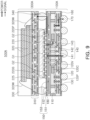
- FIG. 9 is a cross-sectional diagram illustrating an example of a semiconductor package according to an example embodiment.
- a semiconductor package 500A may include a first package structure 100A including a first semiconductor chip 120, and a second semiconductor chip 220 disposed on the first package structure 100A.
- the second semiconductor chip 220 may be mounted on a surface of the first package structure 100A using a connection bump 220B, and the like.
- the semiconductor package 500A in the example embodiment may further include a third package structure 300A disposed on the first package structure 100A with the second semiconductor chip 220 interposed therebetween.
- the third package structure 300A may be mounted on the first package structure 100A in a form of a package-on-package (POP) using a third electrical connector metal 340, and the like.
- An electrical connection path of power and a signal is as in the diagram, for example.
- the first package structure 100A may include a first semiconductor chip 120 having a plurality of first connection pads 120P, a first encapsulant 130 covering at least a portion of the first semiconductor chip 120, a first connection member 140 disposed on a lower side of each of the first encapsulant 130 and the first semiconductor chip 120 and including one or more first redistribution layers 142, and a backside connection member 150 disposed on an upper side of the first encapsulant 130 and including one or more backside wiring layer 152.
- the first package structure 100A may further include a first interconnect member 110 disposed between the first connection member 140 and the backside connection member 150 and electrically connecting the first redistribution layer 142 to the backside wiring layer 152.
- a first passivation layer 160 and a first electrical connector metal 170 may be disposed on a lower side of the first connection member 140.
- a cover layer 180 may be disposed on an upper side of the backside connection member 150.
- the first semiconductor chip 120 includes a through-via 120V penetrating the first semiconductor chip 120.
- the through-via 120V is electrically connected to the first redistribution layer 142 of the first connection member 140 and to the backside wiring layer 152 of the backside connection member 150.
- the second semiconductor chip 220 may overlap the first semiconductor chip 120 on a plane in a vertical direction in which the first semiconductor chip 120 and the second semiconductor chip 220 are stacked. At least a portion of a plurality of second connection pads 220P of the second semiconductor chip 220 may pass through the backside wiring layer 152, the through-via 120V, and the first redistribution layer 142 almost vertically and may be electrically connected to the first electrical connector metal 170. Accordingly, a path for the transfer of power, and the like, may be significantly reduced.
- the first semiconductor chip 120 includes an electronic component 120C disposed in the first semiconductor chip 120 and electrically connected to the through-via 120V.
- the electronic component 120C may be implemented as a metal-insulator-metal (MIM) type capacitor, for example. Accordingly, power properties may improve effectively.
- the electronic component 120C may be implemented as a certain memory unit, an SRAM, for example. Accordingly, an SRAM may not be provided or a size of an SRAM may be reduced in the second semiconductor chip 220 such that a size of the second semiconductor chip 220 may be reduced.
- the electronic component 120C may include both of the above-described capacitor and the memory unit.
- the first semiconductor chip 120 and the second semiconductor chip 220 may operate together as a semiconductor chip to implement a specific function.
- the first semiconductor chip 120 and the second semiconductor chip 220 may implement a function of at least one application process.
- the first semiconductor chip 120 and the second semiconductor chip 220 may be configured by dividing a certain semiconductor chip, such as an application processor chip, into a plurality of semiconductor chips such as first semiconductor chip 120 and the second semiconductor chip 220. By the division, a size of the second semiconductor chip 220 including a core unit may be reduced, and performance may be optimized.
- a defect in one of the processes of manufacturing the first semiconductor chip 120 and the second semiconductor chip 220 may not affect the other such that yield may improve and costs may be reduced.
- the first semiconductor chip 120 may include an input and output unit of an application processor.
- the plurality of second connection pads 220P may include a plurality of pads for input and output operations of an application processor.
- a central semiconductor chip may include a core unit such as a central processing unit (CPU), a graphics processing unit (GPU), a neural processing unit (NPU), a digital signal processor unit (DSPU), an image signal processing unit (ISPU), and the like.
- the plurality of second connection pads 220P may include a plurality of first groups G1 for such core units.
- the second semiconductor chip 220 may further include an input and output (I/O) unit for electrical connection with a memory.
- the plurality of second connection pads 220P may include a plurality of second groups G2 for input and output operations in relation to a memory.
- the memory may be implemented by a DRAM, and may be configured as a third semiconductor chip 320 of a third package structure 300A.
- the first package structure 100A may include the first connection member 140 having the first redistribution layer 142, the first semiconductor chip 120 having the plurality of first connection pads 120P connected to the first redistribution layer 142, the first encapsulant 130 disposed on the first connection member 140 and covering at least a portion of the first semiconductor chip 120, the backside connection member 150 disposed on the first encapsulant 130 and having a backside wiring layer 152 electrically connected to the first redistribution layer 142, and the interconnect member 110 disposed between the first connection member 140 and the backside connection member 150 and electrically connecting the first redistribution layer 142 to the backside wiring layer 152.
- the first passivation layer 160 and the first electrical connector metal 170 may be disposed on a lower side of the first connection member 140.
- the cover layer 180 may be disposed on an upper side of the backside connection member 150.
- the interconnect member 110 may be disposed between the first connection member 140 and the backside connection member 150, may penetrate the first encapsulant 130, and may electrically connect the first redistribution layer 142 to the backside wiring layer 152.
- the interconnect member 110 may include a metal material such as copper (Cu), aluminum (Al), silver (Ag), tin (Sn), gold (Au), nickel (Ni), lead (Pb), titanium (Ti) or alloys thereof.
- the interconnect member 110 may have a post shape penetrating the first encapsulant 130.
- the interconnect member 110 may be formed by encapsulating a post including a conductive material with the first semiconductor chip 120 using the first encapsulant 130.
- An upper surface of the interconnect member 110 may be coplanar with an upper surface of the first encapsulant 130 and an upper surface of the first semiconductor chip 120.
- an upper surface of the interconnect member 110 may be covered by the first encapsulant 130, and in this case, the interconnect member 110 may be connected to the backside wiring layer 152 by a backside via 153 penetrating the first encapsulant 130.
- the first semiconductor chip 120 may be implemented as an integrated circuit (IC) in which several hundreds to several millions of elements are integrated in a single chip.
- the integrated circuit included in the first semiconductor chip 120 may be implemented as, for example, an application processor chip, a partial unit of which is separated and omitted as described above.
- the first semiconductor chip 120 may be configured as an integrated circuit in a bare state which does not include a bump or a wiring layer. However, embodiments are not limited thereto, and the first semiconductor chip 120 may be configured as a packaged type integrated circuit.
- the integrated circuit may be formed based on an active wafer.
- the first connection pad 120P is configured to electrically connect the first semiconductor chip 120 to the other element, and as a material of the first connection pad 120P, a metal material such as copper (Cu), aluminum (Al), or the like, may be used.
- a passivation film for opening the first semiconductor chip 120 may be disposed on the body.
- the passivation film may be implemented by an oxide film or a nitride film, or may be implemented by a double layer including an oxide film and a nitride film.
- An insulating layer, and the like, may be disposed on other positions.
- the first encapsulant 130 may cover at least a portion of the first semiconductor chip 120 and the first interconnect member 110.
- the first encapsulant 130 may include an insulating material, and as an insulating material, a non-photosensitive insulating material, a non-photosensitive insulating material including an inorganic filler and an insulating resin, such as a thermosetting resin such as an epoxy resin, a thermoplastic resin such as polyimide, a resin formed by the above-described resin including a reinforcement such as an inorganic filler, that is, an Ajinomoto Built-up Film (ABF), an epoxy molded compound (EMC), or the like, may be used.
- ABS Ajinomoto Built-up Film
- EMC epoxy molded compound
- a material in which an insulating resin such as a thermosetting resin or a thermoplastic resin is impregnated in a core material such as an inorganic filler and/or a glass fiber may be used. Accordingly, the issues of voids and undulation may be prevented or reduced, and warpage control may be more easily performed.
- a photoimageable encapsulant (PIE) may be used.
- the first connection member 140 may redistribute the first connection pad 120P and/or the second connection pad 220P.
- Each of a plurality of the first connection pad 120P and/or the second connection pad 220P having various functions may be redistributed through the first connection member 140, and the plurality of the first connection pad 120P and/or the second connection pad 220P may be physically and/or electronically connected to an external entity through the first electrical connector metal 170 in accordance with respective functions of the connection pads.
- the first connection member 140 may include a first insulating layer 141, the first redistribution layer 142 disposed on a lower surface of the first insulating layer 141, and a first connection via 143 penetrating the first insulating layer 141 and connected to the first redistribution layer 142.
- the number of each of the first insulating layer 141, the first redistribution layer 142, and the first connection via 143 may be greater or less than the examples illustrated in the diagram. In other words, the number of the layers may be varied in example embodiments.
- an insulating material may be used, and as an insulating material, a photosensitive insulating material (PID) may be used.
- PID photosensitive insulating material
- a fine pitch may be introduced through a photo-via such that it may be possible to implement a fine circuit and a high-density design, and the plurality of first connection pad 120P and/or the second connection pad 220P may be redistributed in a more effective manner.
- a boundary between the first insulating layers 141 may be distinct or indistinct.
- the first redistribution layer 142 may redistribute the plurality of first connection pad 120P and/or the second connection pad 220P and may electrically connect the plurality of first connection pad 120P and/or the second connection pad 220P to the first electrical connector metal 170.
- a metal material such as copper (Cu), aluminum (Al), silver (Ag), tin (Sn), gold (Au), nickel (Ni), lead (Pb), titanium (Ti), or alloys thereof may be used.
- the first redistribution layer 142 may perform various functions.
- the first redistribution layer 142 may include a ground (GND) pattern, a power (PWR) pattern, a signal (S) pattern, and the like.
- the ground (GND) pattern and the power (PWR) pattern may be the same pattern.
- the first redistribution layer 142 may also include various types of via pads, electrical connector metal pads, and the like.
- the first redistribution layer 142 may be formed by a plating process, and may include a seed layer and a conductor layer.
- the first connection via 143 may electrically connect the first redistribution layers 142 disposed on different levels to each other.
- the first connection via 143 may also electrically connect the first connection pad 120P of the first semiconductor chip 120 and the first interconnect member 110 to the first redistribution layers 142.
- the first connection via 143 may be physically in contact with the first connection pad 120P when the first semiconductor chip 120 is a bare die.
- a metal material such as copper (Cu), aluminum (Al), silver (Ag), tin (Sn), gold (Au), nickel (Ni), lead (Pb), titanium (Ti), or alloys thereof may be used.
- the first connection via 143 may include a via for a signal, a via for power, a via for ground, and the like, and a via for power and a via for ground may be the same via.
- the first connection via 143 may also be a filled type via filled with a metal material, or may be a conformal type via in which a metal material is formed along a wall of a via hole.
- the first connection via 143 may have a tapered shape, tapered in a direction opposite to a tapered direction of first wiring vias 113a and 113b.
- the first connection via 143 may also be formed by a plating process, and may include a seed layer and a conductor layer.
- the backside connection member 150 may redistribute the second connection pads 220P. Each of the second connection pads 220P having various functions may be redistributed through the backside connection member 150.
- the backside connection member 150 may include a backside insulating layer 151, a backside wiring layer 152 disposed on an upper surface of the backside insulating layer 151, a backside via 153 penetrating the backside insulating layer 151 and connected to the backside wiring layer 152.
- the number of each of the backside insulating layer 151, the backside wiring layer 152, and the backside via 153 may vary according to example embodiments.
- the backside insulating layer 151 may include a thermosetting resin.
- the backside insulating layer 151 may be an ABF.
- the backside insulating layer 151 may include a PID similar to the first insulating layer 141.
- a boundary between a plurality of the backside insulating layers 151 may be distinct or indistinct.
- the backside wiring layer 152 may be disposed on the first encapsulant 130 and may provide a backside circuit to the first package structure 100A along with the backside via 153.
- the backside wiring layer 152 may include a metal material such as copper (Cu), aluminum (Al), silver (Ag), tin (Sn), gold (Au), nickel (Ni), lead (Pb), titanium (Ti), or alloys thereof.
- the backside wiring layer 152 may perform various functions according to example embodiments.
- the backside wiring layer 152 may include a ground (GND) pattern, a power (PWR) pattern, a signal (S) pattern, and the like.
- the signal (S) pattern may include various types of signals such as a data signal other than the ground (GND) pattern, the power (PWR) pattern, and the like.
- the ground (GND) pattern and the power (PWR) pattern may be the same pattern.
- the backside wiring layer 152 may be formed by a plating process, and may include a seed layer and a conductor layer.
- the backside via 153 may penetrate the first encapsulant 130 and/or the backside insulating layer 151.
- the backside via 153 may electrically connect the backside wiring layer 152 to a 1-3 wiring layer 112c.
- the backside via 153 may also electrically connect the backside wiring layers 152 disposed on different levels to each other.
- the backside via 153 may include a metal material such as copper (Cu), aluminum (Al), silver (Ag), tin (Sn), gold (Au), nickel (Ni), lead (Pb), titanium (Ti), or alloys thereof.
- the backside via 153 may be a filled type via filled with a metal material, or may be a conformal type via in which a metal material is formed along a wall of a via hole.
- the backside via 153 may have a tapered shape, tapered in the same direction as a tapered direction of the first wiring vias 113a and 113b.
- the backside via 153 may include a via for a signal, a via for power, a via for ground, and the like, and a via for power and a via for ground may be the same via.
- the backside via 153 may be formed by a plating process, and may include a seed layer and a conductor layer.
- the first passivation layer 160 may be an additional element which may protect the first connection member 140 from external physical and chemical damages, and other damages.
- the first passivation layer 160 may include a thermosetting resin.
- the first passivation layer 160 may be an ABF, but example embodiments are not limited thereto.
- the first passivation layer 160 may have an opening exposing at least a portion of a lowermost first redistribution layer 142. Several tens to several millions of the openings may be provided on the first passivation layer 160, or the number of the openings may be higher or lower than the aforementioned example. Each of the openings may include a plurality of holes.
- a surface mount component such as a capacitor may be disposed on a lower surface of the first passivation layer 160 such that the first passivation layer 160 may be electrically connected to the first redistribution layer 142, and the first passivation layer 160 may also be electrically connected to the first semiconductor chip 120.
- the first electrical connector metal 170 may also be an additional element, and may physically and/or electronically connect the semiconductor package 500A with an external entity.
- the semiconductor package 500A according to the example embodiment may be mounted on a mainboard of an electronic device through the first electrical connector metal 170.
- the first electrical connector metal 170 may be disposed on each of the openings of the first passivation layer 160.
- the first electrical connector metal 170 may be formed of a low melting point metal, such as tin (Sn) or an alloy including tin (Sn), for example.
- the first electrical connector metal 170 may be formed of solder, or the like, but example embodiments are not limited thereto.
- the first electrical connector metal 170 may be implemented as a land, a ball, a pin, or the like.
- the first electrical connector metal 170 may include multiple layers or a single layer.
- the first electrical connector metal 170 may include a copper pillar and solder, and when the first electrical connector metal 170 includes a single layer, the first electrical connector metal 170 may include tin-silver solder or copper, but example embodiments are not limited thereto.
- the number of the first electrical connector metal 170, a gap between the first electrical connector metals 170, and a dispositional form of the first electrical connector metal 170 are not limited to any particular example, and may be varied according to the example embodiments.
- the number of the first electrical connector metal 170 may be several tens to several millions in accordance with the number of the plurality of first connection pad 120P and/or the second connection pad 220P, and may be higher or lower than the above-mentioned example.
- At least one of the first electrical connector metals 170 may be disposed in a fan-out region.
- a fan-out region may refer to a region beyond a region in which the first semiconductor chip 120 and the second semiconductor chip 220 are disposed.
- a fan-out package may have improved reliability as compared to a fan-in package, may implement a plurality of I/O terminals, and may easily perform 3D interconnection. Also, a fan-out package may have a reduced thickness as compared to a BGA package, a land grid array (LGA) package, and the like, and may be cost-competitive.
- LGA land grid array
- the first electrical connector metal 170 may be connected to a lowermost first redistribution layer 142 through an underbump metal if desired, and in this case, connection reliability of the first electrical connector metal 170 may improve. Accordingly, board-level reliability of the first package structure 100A may be improved.
- the underbump metal may be formed by a well-known metallization method using a metal, but an example embodiment thereof is not limited thereto.
- the cover layer 180 may be an additional element for protecting the backside connection member 150 from external physical and chemical damages, and others.
- the cover layer 180 may include thermosetting resin.
- the cover layer 180 may be an ABF, but an example embodiment thereof is not limited thereto.
- the cover layer 180 may have an opening for opening at least a portion of an uppermost backside wiring layer 152. Several tens to several millions of the openings may be provided, or the number of the openings may be higher or lower than the above-mentioned example. Each of the openings may include a plurality of holes.
- the second semiconductor chip 220 may be disposed on the first package structure 100A (the first connection member 140 or the backside connection member 150).
- the second semiconductor chip 220 may be mounted on a surface of the backside connection member 150 of the first package structure 100A using a connection bump 220B, or the like.
- the second semiconductor chip 220 may be fixed on the first package structure 100A through an underfill resin 225.
- the second semiconductor chip 220 may be configured as an integrated circuit IC in which several hundreds to several millions of elements are integrated in a single chip.
- An integrated circuit included in the second semiconductor chip 220 may be configured as an application processor, a partial unit of which is separated and omitted as described above.
- the second semiconductor chip 220 may be configured as an integrated circuit in a bare state in which a bump or a wiring layer is not formed. However, an example embodiment thereof is not limited thereto, and the second semiconductor chip 220 may be configured as a packaged type integrated circuit if desired.
- the integrated circuit may be formed based on an active wafer.
- the body of the second semiconductor chip 220 silicon (Si), germanium (Ge), gallium arsenide (GaAs), or the like, may be used as a base material of the body of the second semiconductor chip 220.
- the body may include various circuits.
- the second connection pad 220P may electrically connect the second semiconductor chip 220 to the other element, and a metal material such as copper (Cu), aluminum (Al), or the like, may be used as a material for the second connection pad 220P.
- a passivation film for protecting the second semiconductor chip 220 may be formed on the body.
- the passivation film may be an oxide film, a nitride file, or the like, or may be a dual layer including an oxide film and a nitride file.
- An insulating film, or the like may also be disposed in other desired positions.
- connection bump 220B the second semiconductor chip 220 may be mounted on the first package structure 100A, on a surface of the cover layer 180, for example.
- the connection bump 220B may be connected to each of the uppermost backside wiring layers 152 exposed through the openings of the cover layer 180.
- the connection bump 220B may be formed of a low melting point metal, tin (Sn) or an alloy including tin (Sn), for example.
- the connection bump 220B may be a solder bump formed of a solder paste, but an example embodiment thereof is not limited thereto.
- the underfill resin 225 may fasten the second semiconductor chip 220 by filling a region between the second semiconductor chip 220 and a cover layer 180.
- the underfill resin 225 may cover at least a portion of each of the connection bumps 220B.
- the underfill resin 225 may cover at least a portion of a side surface of the second semiconductor chip 220.
- the underfill resin 225 may include epoxy, but a material of the underfill resin 225 is not limited thereto.
- the third package structures 300A may be disposed on the first package structure 100A with the second semiconductor chip 220 interposed therebetween.
- the third package structure 300A may be mounted on the first package structure 100A in a form of POP using the third electrical connector metal 340, and the like.
- the third package structure 300A may include a printed circuit board 310 (or may be referred to as "third connection member"), a plurality of third semiconductor chips 320 stacked and disposed on an upper side of the printed circuit board 310 and electrically connected to the printed circuit board 310 through a wiring bonding 320W, a molding material 330 disposed on an upper side of the printed circuit board 310 and covering the third semiconductor chip 320, and the third electrical connector metal 340 disposed on a lower side of the printed circuit board 310 and connecting the first and third package structures 100A and 300A to each other.
- Each of the plurality of third semiconductor chips 320 may be implemented as a memory chip, a DRAM, for example.
- the third package structure 300A may be configured as a DRAM package.
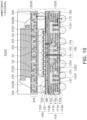
- FIG. 10 is a cross-sectional diagram illustrating another example of a semiconductor package according to an example embodiment.
- an interconnect member 110 may be configured as a first frame 110 having a first through portion 110H in which a first semiconductor chip 120 is disposed.
- a first package structure 100B may include the first frame 110 having the first through portion 110H and including one or more first wiring layers 112a, 112b, and 112c, a first semiconductor chip 120 disposed within the first through portion 110H and having a plurality of first connection pads 120P, a first encapsulant 130 covering at least a portion of each of the first frame 110 and the first semiconductor chip 120 and filling at least a portion of the first through portion 110H, a first connection member 140 disposed on a lower side of each of the first frame 110 and the first semiconductor chip 120 and including one or more first redistribution layers 142, and a backside connection member 150 disposed on an upper side of the first encapsulant 130 and including one or more backside wiring layers 152.
- the first frame 110 may improve stiffness of the first package structure 100A depending on a specific material of insulating layers 111a and 11 1b, and may secure uniformity of a thickness of the first encapsulant 130.
- the first frame 110 may have the first through portion 110H penetrating the insulating layers 111a and 111b.
- the first semiconductor chip 120 may be disposed within the first through portion 110H, and if desired, a passive component may also be disposed in the first through portion 110H.
- a wall of the first through portion 110H may surround the first semiconductor chip 120, but an example embodiment thereof is not limited thereto.
- the first frame 110 may include the first wiring layers 112a, 112b, and 112c and first wiring vias 113a and 113b in addition to the insulating layers 111a and 111b, and may work as an electrical connection member providing upper and lower electrical connection paths. If desired, an electrical connection member which may provide a different form of upper and lower electrical connection paths, such as a metal post, may be included in the first frame 110.
- the first frame 110 may include a 1-1st insulating layer 111a, a 1-1st wiring layer 112a in contact with the first connection member 140 and buried in the 1-1st insulating layer 111a, a 1-2nd wiring layer 112b disposed in a region opposite to the region of the 1-1st insulating layer 111a in which the 1-1st wiring layer 112a is buried, a 1-2nd insulating layer 111b disposed in a region opposite to the region of the 1-1 st insulating layer 111a in which the 1-1st wiring layer 112a is buried, and covering at least a portion of the 1-2nd wiring layer 112b, and a 1-3rd wiring layer 112c disposed in a region opposite to the region of the 1-2nd insulating layer 11 1b in which the 1-2nd wiring layer 112b is buried.
- the 1-1st and 1-2nd wiring layers 112a and 112b and the 1-2nd and 1-3rd wiring layers 112b and 112c may be connected to each other through the 1-1st and 1-2nd wiring vias 113a and 113b penetrating the 1-1st and 1-2nd insulating layers 111a and 11 1b, respectively.
- the 1-1st to 1-3rd wiring layers 112a, 112b, and 112c may be electrically connected to a plurality of the first and/or second connection pads 120P and 220P.
- a material of the insulating layers 111a and 111b is not limited to any particular material.
- an insulating material may be used, and as an insulating material, a thermosetting resin such as an epoxy resin, a thermoplastic resin such as polyimide, a resin in which the thermosetting resin or the thermoplastic resin is mixed with an inorganic filler, an ABF, for example, may be used.
- a material in which the above-mentioned resin is impregnated together with an inorganic filler in a core material such as a glass fiber (or a glass cloth or a glass fabric), such as prepreg, may be used.
- the first wiring layers 112a, 112b, and 112c may provide upper/lower electrical connection paths of the package along with the first wiring vias 113a and 113b, and may redistribute the first connection pad 120P and/or the second connection pad 220P.
- a metal material such as copper (Cu), aluminum (Al), silver (Ag), tin (Sn), gold (Au), nickel (Ni), lead (Pb), titanium (Ti), or alloys thereof may be used.
- the first wiring layers 112a, 112b, and 112c may perform various functions in accordance with a design of a respective layer.
- the first wiring layers 112a, 112b, and 112c may include a ground (GND) pattern, a power (PWR) pattern, a signal (S) pattern, and the like.
- the signal (S) pattern may include various types of signals such as a data signal other than the ground (GND) pattern, the power (PWR) pattern, and the like.
- the ground (GND) pattern and the power (PWR) pattern may be the same pattern.
- the first wiring layers 112a, 112b, and 112c may include various types of via pads.
- the first wiring layers 112a, 112b, and 112c may be formed by a plating process, and may include a seed layer and a conductor layer.
- a thickness of each of the first wiring layers 112a, 112b, and 112c may be greater than a thickness of each of the first redistribution layers 142.
- the first frame 110 may have a thickness greater than a thickness of the first semiconductor chip 120, and prepreg, or the like, may be used as a material of the insulating layers 11 1a and 111b to maintain stiffness. Accordingly, a thickness of each of the first wiring layers 112a, 112b, and 112c may be relatively increased.
- a fine circuit and a high-density design may be required for the first connection member 140, and a photosensitive insulating material PID, or the like, may be used as a material of the first insulating layer 141. Accordingly, a thickness of the first redistribution layer 142 may be relatively decreased.
- the 1-1 st wiring layer 112a may be recessed into the 1-1 st insulating layer 111a.
- a stepped portion is formed between a lower surface in contact with the first connection member 140 of the 1-1 st insulating layer 111a and a lower surface in contact with the first connection member 140 of the 1-1st wiring layer 112a as the 1-1st wiring layer 112a is recessed into the 1-1st insulating layer 111a
- a forming material may be bled when the first semiconductor chip 120 and the interconnect member 110 are capsulated using the first encapsulant 130 such that contamination of a lower surface of the 1-1st wiring layer 112a may be prevented.
- the first wiring vias 113a and 113b may electrically connect the first wiring layers 112a, 112b, and 112c disposed on different levels to one another, and may accordingly form an electrical path in the first frame 110.
- a metal material such as copper (Cu), aluminum (Al), silver (Ag), tin (Sn), gold (Au), nickel (Ni), lead (Pb), titanium (Ti), or alloys thereof may be used.
- the first wiring vias 113a and 113b may include a via for a signal, a via for power, a via for ground, and the like, and a via for power and a via for ground may be the same via.
- the first wiring vias 113a and 113b may be a filled type via filled with a metal material, or may be a conformal type via in which a metal material is formed along a wall of a via hole. Each of the first wiring vias 113a and 113b may have a tapered shape.
- the first wiring vias 113a and 113b may also be formed by a plating process, and may include a seed layer and a conductor layer.
- a partial pad of the 1-1 st wiring layer 112a may work as a stopper.
- the 1-1st wiring via 113a may have a tapered shape in which a width of an upper surface of the 1-1st wiring via 113a may be greater than a width of a lower surface.
- the 1-1st wiring via 113a may be integrated with a pad pattern of the 1-2nd wiring layer 112b.
- a partial pad of the 1-2nd wiring layer 112b may work as a stopper.
- the 1-2nd wiring via 113b may have a tapered shape in which a width of an upper surface of the 1-2nd wiring via 113b may be greater than a width of a lower surface.
- the 1-2nd wiring via 113b may be integrated with a pad pattern of the 1-3rd wiring layer 112c.
- a metal layer may be disposed on an internal wall of the first through portion 110H of the first frame 110 for the purpose of shielding electromagnetic waves or heat dissipation.
- the metal layer may surround the first semiconductor chip 120.
- the first encapsulant 130 may cover at least a portion of the first semiconductor chip 120 and the first frame 110, and may fill at least a portion of the first through portion 110H.
- the first encapsulant 130 may include an insulating material, and as an insulating material, a non-photosensitive insulating material, a non-photosensitive insulating material including an inorganic filler and an insulating resin, such as a thermosetting resin such as an epoxy resin, a thermoplastic resin such as polyimide, a resin formed by the above-described resin including a reinforcement such as an inorganic filler, that is, an ABF, an EMC, or the like, may be used.
- a material in which an insulating resin such as a thermosetting resin or a thermoplastic resin is impregnated in a core material such as an inorganic filler and/or a glass fiber may be used. Accordingly, the issues of void and undulation may be resolved, and warpage control may be easily performed.
- a photoimageable encapsulant (PIE) may be used.
- the 1-3rd wiring layer 112c of the first frame 110 may be covered by the first encapsulant 130, and the backside via 153 may penetrate the first encapsulant 130 and may connect the 1-3rd wiring layer 112c to the backside wiring layer 152.
- an example embodiment thereof is not limited thereto, and an upper surface of the 1-3rd wiring layer 112c may be directly in contact with the backside insulating layer 151, and the backside via 153 may penetrate the backside insulating layer 151 directly in contact with the upper surface of the 1-3rd wiring layer 112c and may connect the 1-3rd wiring layer 112c to the backside wiring layer 152.
- FIG. 11 is a cross-sectional diagram illustrating another example of a semiconductor package according to an example embodiment.
- a first package structure 100C may be disposed upside down, differently from the aforementioned first package structure 100A, to dispose a first semiconductor chip 120 to be faced-up.
- a second semiconductor chip 220 may be mounted on a surface of a first connection member 140 of a first package structure 100C using a connection bump 220B, and the like.
- the second semiconductor chip 220 may be fastened to the first package structure 100C through an underfill resin 225. In this case, an electrical connection path between the first and second semiconductor chips 120 and 220 may be shortened.
- the second semiconductor chip 220 may be disposed on a first passivation layer 160, and a third package structures 300C may be disposed on the first passivation layer 160 with the second semiconductor chip 220 interposed therebetween.
- An electrical connection path of power and a signal may be as in the diagram, for example.
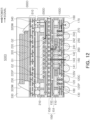
- FIG. 12 is a cross-sectional diagram illustrating another example of a semiconductor package according to an example embodiment.
- a second package structure 200D may be disposed between first and third package structures 100D and 300D.
- the first and second package structures 100D and 200D may be connected to each other in a form of POP through a second electrical connector metal 270.
- the second and third package structures 200D and 300D may be connected to each other in a form of POP through a third electrical connector metal 340.
- the second package structure 200D may include a second connection member 240 disposed on a first connection member 140 or a backside connection member 150 and having a second redistribution layer 242 connected to a first redistribution layer 142 or a backside wiring layer 152, a second semiconductor chip 220 having a plurality of second connection pads 220P connected to the second redistribution layer 242, and a second encapsulant 230 disposed on the second connection member 240 and covering the second semiconductor chip 220.
- the second package structure 200D may further include a second interconnect member 210 disposed on the second connection member 240 and electrically connected to the second redistribution layer 242.
- the second interconnect member 210 may electrically connect the second redistribution layer 242 to a third electrical connector metal 340.
- the second connection member 240 may be mounted on the backside connection member 150 through a second electrical connector metal 270.
- the second encapsulant 230 may cover at least a portion of the second semiconductor chip 220 and the second interconnect member 210.
- the second encapsulant 230 may include an insulating material, as an insulating material, a non-photosensitive insulating material, a non-photosensitive insulating material including an inorganic filler and an insulating resin, such as a thermosetting resin such as an epoxy resin, a thermoplastic resin such as polyimide, a resin formed by the above-described resin including a reinforcement such as an inorganic filler, that is, an ABF, an EMC, or the like, may be used.
- a material in which an insulating resin such as a thermosetting resin or a thermoplastic resin is impregnated in a core material such as an inorganic filler and/or a glass fiber may be used. Accordingly, the issues of void and undulation may be resolved, and warpage control may be easily performed.
- a photoimageable encapsulant (PIE) may be used.
- the second connection member 240 may redistribute the plurality of second connection pads 220P.
- Each of the plurality of second connection pads 220P having various functions may be redistributed through the second connection member 240, and may be physically and/or electronically connected to an external entity through the second electrical connector metal 270 in accordance with a function thereof.
- the second connection member 240 may include a second insulating layer 241, a second redistribution layer 242 disposed on a lower surface of the second insulating layer 241, and a second connection via 243 penetrating the second insulating layer 241 and connected to the second redistribution layer 242.
- the number of each of the second insulating layer 241, the second redistribution layer 242, and the second connection via 243 may be greater or lower than the examples illustrated in the diagram. In other words, in example embodiments, the number of the layers may be varied.
- an insulating material may be used, and as an insulating material, a photosensitive insulating material (PID) may be used.
- PID photosensitive insulating material
- a fine pitch may be introduced through a photo-via such that it may be possible to implement a fine circuit and a high-density design, and the plurality of second connection pads 220P may be redistributed in an effective manner.
- a boundary between the second insulating layer 241 may be distinct or indistinct.
- the second redistribution layer 242 may redistribute the plurality of second connection pads 220P and may electrically connect the plurality of second connection pads 220P to the second electrical connector metal 270.
- a metal material such as copper (Cu), aluminum (Al), silver (Ag), tin (Sn), gold (Au), nickel (Ni), lead (Pb), titanium (Ti), or alloys thereof may be used as a material for the second redistribution layer 242.
- the second redistribution layer 242 may perform various functions in example embodiments.
- the second redistribution layer 242 may include a ground (GND) pattern, a power (PWR) pattern, a signal (S) pattern, and the like.
- the ground (GND) pattern and the power (PWR) pattern may be the same pattern.
- the second redistribution layer 242 may include various types of via pads, electrical connector metal pads, and the like.
- the second redistribution layer 242 may be formed by a plating process, and may include a seed layer and a conductor layer.
- the second connection via 243 may electrically connect the second redistribution layers 242 disposed on different levels to one another.
- the second connection via 243 may also electrically connect the second connection pad 220P of the second semiconductor chip 220 and the second interconnect member 210 to the second redistribution layer 242.
- the second connection via 243 may be physically in contact with the second connection pad 220P when the second semiconductor chip 220 is a bare die.
- a metal material such as copper (Cu), aluminum (Al), silver (Ag), tin (Sn), gold (Au), nickel (Ni), lead (Pb), titanium (Ti), or alloys thereof may be used.
- the second connection via 243 may include a via for a signal, a via for power, a via for ground, and the like, and a via for power and a via for ground may be the same via.
- the second connection via 243 may also be a filled type via filled with a metal material, or may be a conformal type via in which a metal material is formed along a wall of a via hole.
- the second connection via 243 may have a tapered shape, tapered in a direction opposite to a tapered direction of second wiring vias 213a and 213b.
- the second connection via 243 may also be formed by a plating process, and may include a seed layer and a conductor layer.
- a second passivation layer 260 may be an additional element for protecting the second connection member 240 from external physical and chemical damages, and others.
- the second passivation layer 260 may include a thermosetting resin.
- the second passivation layer 260 may be an ABF, but an example embodiment thereof is not limited thereto.
- the second passivation layer 260 may have an opening for opening at least a portion of a lowermost second redistribution layer 242. Several tens to several millions of the openings may be provided, or the number of the openings may be higher or lower than the above-mentioned example. Each of the openings may include a plurality of holes.
- a surface mount component such as a capacitor may be disposed on a lower surface of a second passivation layer 250 and may be electrically connected to the second redistribution layer 242, and may be electrically connected to the second semiconductor chip 220 accordingly.
- the second electrical connector metal 270 may physically and/or electronically connect the first and second package structures 100D and 200D to each other.
- the second electrical connector metal 270 may be disposed in each of the openings of the second passivation layer 250.
- the second electrical connector metal 270 may be formed of a low melting point metal, such as tin (Sn) or an alloy including tin (Sn), for example.
- the second electrical connector metal 270 may be formed of solder, or the like, but an example embodiment thereof is not limited thereto.
- the second electrical connector metal 270 may be implemented as a land, a ball, a pin, or the like.
- the second electrical connector metal 270 may include multiple layers or a single layer.
- the first electrical connector metal 170 may include a copper pillar and solder
- the second electrical connector metal 270 may include tin-silver solder or copper, but an example embodiment thereof is not limited thereto.
- the number of the second electrical connector metal 270, a gap between the second electrical connector metals 270, and a dispositional form of the second electrical connector metal 270 are not limited to any particular example, and may be varied in example embodiments.
- the number of the second electrical connector metal 270 may be several tens to several millions in accordance with the number of the plurality of second connection pads 220P, and may be higher or lower than the above-mentioned example.
- At least one of the second electrical connector metals 270 may be disposed in a fan-out region.
- a fan-out region may refer to a region beyond a region in which the second semiconductor chip 220 is disposed.
- a fan-out package may have improved reliability as compared to a fan-in package, may implement a plurality of I/O terminals, and may easily perform 3D interconnection.
- a fan-out package may have a reduced thickness as compared to a ball grid array (BGA) package, a land grid array (LGA) package, and the like, and may be cost-competitive.
- BGA ball grid array
- LGA land grid array
- the second electrical connector metal 270 may be connected to a lowermost second redistribution layer 242 through an underbump metal, and in this case, connection reliability of the second electrical connector metal 270 may improve. Accordingly, board-level reliability of the second package structure 200D may improve.
- the underbump metal may be formed by a metallization method using a metal, but an example embodiments are not limited thereto.
- FIG. 13 is a cross-sectional diagram illustrating another example of a semiconductor package according to an example embodiment.
- a second interconnect member 210 may be configured as a second frame 210 having a second through portion 210H in which the second semiconductor chip 220 is disposed.
- the semiconductor package 500E may include the second frame 210 having a second through portion 210H and including one or more second wiring layers 212a, 212b, and 212c, a second semiconductor chip 220 disposed in the second through portion 210H and having a plurality of second connection pads 220P, a second encapsulant 230 covering at least a portion of each of the second frame 210 and the second semiconductor chip 220 and filling at least a portion of the second through portion 210H, and a second connection member 240 disposed on a lower side of each of the second frame 210 and the second semiconductor chip 220 and including one or more second redistribution layer 242.
- a second passivation layer 260 and a second electrical connector metal 270 may also be disposed on a lower side of the second connection member 240.
- the second frame 210 may compensate for a height of a third electrical connector metal 340, a pitch of the third electrical connector metal 340 between the second package structure 200E and the third package structure 300E may be reduced.
- the number of inputs and outputs (I/O) of the third package structure 300C, the number of inputs and outputs (I/O) of a memory may increase.
- an electrical connection path of power and a signal may be provided as illustrated in FIG. 13 .
- the second package structure 200E may include a second frame 210 having a second through portion 210H and including one or more layers of second wiring layers 212a, 212b, and 212c, the second semiconductor chip 220 disposed in the second through portion 210H and having a plurality of second connection pads 220P, the second encapsulant 230 covering at least a portion of each of the second frame 210 and the second semiconductor chip 220 and filling at least a portion of the second through portion 210H, and the second connection member 240 disposed on a lower side of each of the second frame 210 and the second semiconductor chip 220 and including one or more layers of the second redistribution layer 242.
- the second passivation layer 260 and the second electrical connector metal 270 may be disposed on a lower side of the second connection member 240.
- the second frame 210 may improve stiffness of the second package structure 200E depending on a specific material of second insulating layers 211a and 21 1b, and may secure uniformity of a thickness of the second encapsulant 230.
- the second frame 210 may have the second through portion 210H penetrating the second insulating layers 211a and 211b.
- the second semiconductor chip 220 may be disposed in the second through portion 210H, and a passive component may also be disposed in the second through portion 210H.
- a wall of the second through portion 210H may surround the second semiconductor chip 220, but example embodiments are not limited thereto.
- the second frame 210 may include the second wiring layers 212a, 212b, and 212c and second wiring vias 213a and 213b in addition to the second insulating layers 211a and 211b, and may work as an electrical connection member providing upper and lower electrical connection paths.
- an electrical connection member which may provide a different form of upper and lower electrical connection paths, such as a metal post, may be included in the second frame 210.
- the second frame 210 may include a 2-1st insulating layer 211a, a 2-1st wiring layer 212a in contact with the second connection member 240 and buried in the 2-1st insulating layer 211a, a 2-2nd wiring layer 212b disposed on a region opposite to the region of the 2-1st insulating layer 211a in which the 2-1st wiring layer 212a is buried, a 2-2nd insulating layer 211b disposed in a region opposite to the region of the 2-1st insulating layer 211a in which the 2-1st wiring layer 212a is buried, and covering at least a portion of the 2-2nd wiring layer 212b, and a 2-3rd wiring layer 212c disposed in a region opposite to the region of the 2-2nd insulating layer 211b in which the 2-2nd wiring layer 212b is buried.
- the 2-1st and 2-2nd wiring layers 212a and 212b and the 2-2nd and 2-3rd wiring layers 212b and 212c may be electrically connected to each other through the 2-1st and 2-2nd wiring vias 213a and 213b penetrating the 2-1st and 2-2nd insulating layers 211a and 211b, respectively.
- the 2-1st to 2-3rd wiring layers 212a, 212b, and 212c may be electrically connected to a plurality of the second connection pads 220P.
- a material of the second insulating layers 211a and 211b is not limited to any particular material.
- an insulating material may be used, and as an insulating material, a thermosetting resin such as an epoxy resin, a thermoplastic resin such as polyimide, a resin in which the thermosetting resin or the thermoplastic resin is mixed with an inorganic filler, an Ajinomoto Built-up Film (ABF), for example, may be used.
- a material in which the above-mentioned resin is impregnated together with an inorganic filler in a core material such as a glass fiber (or a glass cloth or a glass fabric), such as prepreg, may be used.
- the second wiring layers 212a, 212b, and 212c may provide upper/lower electrical connection paths of the package along with the second wiring vias 213a and 213b, and may redistribute the plurality of second connection pads 220P.
- a metal material such as copper (Cu), aluminum (Al), silver (Ag), tin (Sn), gold (Au), nickel (Ni), lead (Pb), titanium (Ti), or alloys thereof may be used.
- the second wiring layers 212a, 212b, and 212c may perform various functions in accordance with a design of a respective layer.
- the second wiring layers 212a, 212b, and 212c may include a ground (GND) pattern, a power (PWR) pattern, a signal (S) pattern, and the like.
- the signal (S) pattern may include various types of signals such as a data signal other than the ground (GND) pattern, the power (PWR) pattern, and the like.
- the ground (GND) pattern and the power (PWR) pattern may be the same pattern.
- the second wiring layers 212a, 212b, and 212c may include various types of via pads.
- the second wiring layers 212a, 212b, and 212c may be formed by a well-known plating process, and may include a seed layer and a conductor layer.
- a thickness of each of the second wiring layers 212a, 212b, and 212c may be greater than a thickness of each of the second redistribution layers 242.
- the second frame 210 may have a thickness greater than a thickness of the second semiconductor chip 220, and prepreg, or the like, may be used as a material of the second insulating layers 211a and 211b to maintain stiffness. Accordingly, a thickness of each of the second wiring layers 212a, 212b, and 212c may be relatively increased.
- a fine circuit and a high-density design may be required for the second connection member 240, and a photosensitive insulating material PID, or the like, may be used as a material of the second insulating layer 241. Accordingly, a thickness of the second redistribution layer 242 may be relatively decreased.
- the 2-1st wiring layer 212a may be recessed into the 2-1st insulating layer 211a.
- a stepped portion is formed between a lower surface in contact with the second connection member 240 of the 2-1 st insulating layer 211a and a lower surface in contact with the second connection member 240 of the 2-1st wiring layer 212a as the 2-1st wiring layer 212a is recessed into the 2-1st insulating layer 211a
- a forming material may be bled when the second semiconductor chip 220 and the second frame 210 are capsulated using the second encapsulant 230 such that contamination of a lower surface of the 2-1st wiring layer 212a may be prevented.
- the second wiring vias 213a and 213b may electrically connect the second wiring layers 212a, 212b, and 212c disposed on different levels to one another, and may accordingly form an electrical path in the second frame 210.
- a metal material such as copper (Cu), aluminum (Al), silver (Ag), tin (Sn), gold (Au), nickel (Ni), lead (Pb), titanium (Ti), or alloys thereof may be used.
- the second wiring vias 213a and 213b may include a via for a signal, a via for power, a via for ground, and the like, and a via for power and a via for ground may be the same via.
- the second wiring vias 213a and 213b may be a filled type via filled with a metal material, or may be a conformal type via in which a metal material is formed along a wall of a via hole. Each of the second wiring vias 213a and 213b may have a tapered shape.
- the second wiring vias 213a and 213b may also be formed by a plating process, and may include a seed layer and a conductor layer.
- the 2-1st wiring via 213a may have a tapered shape in which a width of an upper surface of the 2-1st wiring via 213a may be greater than a width of a lower surface of the 2-1st wiring via 213a.
- the 2-1st wiring via 213a may be integrated with a pad pattern of the 2-2nd wiring layer 212b.
- a partial pad of the 2-2nd wiring layer 212b may work as a stopper.
- the 2-2nd wiring via 213b may have a tapered shape in which a width of an upper surface of 2-2nd wiring via 213b may be greater than a width of a lower surface of 2-2nd wiring via 213b.
- the 2-2nd wiring via 213b may be integrated with a pad pattern of the 2-3 wiring layer 212c.
- a metal layer may be disposed on an internal wall of the second through portion 210H of the second frame 210 to shield electromagnetic waves or heat dissipation.
- the metal layer may surround the second semiconductor chip 220.
- the second encapsulant 230 may cover at least a portion of the second semiconductor chip 220 and the second frame 210, and may fill at least a portion of the second through portion 210H.
- the second encapsulant 230 may include an insulating material, and as an insulating material, a non-photosensitive insulating material, a non-photosensitive insulating material including an inorganic filler and an insulating resin, such as a thermosetting resin such as an epoxy resin, a thermoplastic resin such as polyimide, a resin formed by the above-described resin including a reinforcement such as an inorganic filler, that is, an ABF, an EMC, or the like, may be used.
- a material in which an insulating resin such as a thermosetting resin or a thermoplastic resin is impregnated in a core material such as an inorganic filler and/or a glass fiber may be used. Accordingly, the issues of void and undulation may be prevented or reduced, and warpage control may be more easily performed.
- a photoimageable encapsulant (PIE) may be used.
- FIG. 14 is a cross-sectional diagram illustrating another example of a semiconductor package according to an example embodiment.
- a first package structure 100F may be disposed upside down, different from the aforementioned first package structure 100A, to dispose a first semiconductor chip 120 to be faced-up.
- a second semiconductor chip 220 may be mounted on a surface of a first connection member 140 of a first package structure 100F using a connection bump 220B, and the like.
- the second semiconductor chip 220 may be fastened to the first package structure 100F through an underfill resin.
- a second package structure 200F may be disposed between first package structure 100F and the third package structure 300F.
- the first package structure 100F and the second package structure 200F may be connected to each other in a form of POP through the second electrical connector metal.
- Second package structure 200F and the third package structure 300F may be connected to each other in a form of POP through an third electrical connector metal 340.
- an electrical connection path of power and a signal may be as provided as illustrated in FIG. 14 .
- the second package structure 200F may include a second frame 210 having a second through portion 210H and including one or more second wiring layers 212a, 212b, and 212c, the second semiconductor chip 220 disposed in the second through portion 210H and having a plurality of second connection pads 220P, the second encapsulant 230 covering at least a portion of each of the second frame 210 and the second semiconductor chip 220 and filling at least a portion of the second through portion 210H, and the second connection member 240 disposed on a lower side of each of the second frame 210 and the second semiconductor chip 220 and including one or more second redistribution layers.
- the second passivation layer and the second electrical connector metal may be disposed on a lower side of the second connection member 240.
- a semiconductor package having improved package performance and having an appropriate package size may be provided.
- a lower side, a lower portion, a lower surface, and the like may refer to a downward direction with reference to a cross-sectional surface in the diagram, and an upper side, an upper portion, an upper surface, and the like, may refer to an opposite direction.
- the directions, however, may be defined for ease of descriptions, and a scope of the claims is not limited thereto, and the terminology may be varied.
- one example embodiment may not refer to the same example embodiment, and may be provided to emphasize different unique features.
- the aforementioned example embodiments do not exclude combination or addition of one or more features of another example embodiment.
- matters described in one example embodiment are not described in another example embodiment, the matters may be understood as being related to another example embodiment unless otherwise indicated.
Landscapes
- Production Of Multi-Layered Print Wiring Board (AREA)
- Engineering & Computer Science (AREA)
- Microelectronics & Electronic Packaging (AREA)
- Semiconductor Integrated Circuits (AREA)
Claims (7)
- Halbleitergehäuse (500A), Folgendes umfassend:eine Gehäusestruktur (100A) umfassend ein Basisverbindungselement (140), das eine Umverteilungsschicht (142), einen ersten Halbleiterchip (120), der eine Vielzahl von ersten Anschlussflächen (120P) umfasst, die mit der Umverteilungsschicht verbunden sind, ein Verkapselungsstoff (130), der auf dem Basisverbindungselement angeordnet ist und mindestens einen Abschnitt des ersten Halbleiterchips bedeckt, ein Rückseiten-Verbindungselement (150), das auf dem Verkapselungsstoff angeordnet ist und eine Rückseiten-Verdrahtungsschicht (152) umfasst, die elektrisch mit der Umverteilungsschicht verbunden ist, eine Durchkontaktierung (120V), die die Umverteilungsschicht mit der Rückseiten-Verdrahtungsschicht verbindet, indem sie den ersten Halbleiterchip durchdringt, und eine elektronische Komponente (120C) umfasst, die innerhalb des ersten Halbleiterchips angeordnet und elektrisch mit der Durchkontaktierung verbunden ist;einen zweiten Halbleiterchip (220), der auf dem Basisverbindungselement oder dem Rückseiten-Verbindungselement angeordnet ist, wobei der zweite Halbleiterchip eine Vielzahl von zweiten Anschlussflächen (220P) umfasst, die mit der Umverteilungsschicht oder der Rückseiten-Verdrahtungsschicht verbunden sind; undeine Vielzahl von Verbindungshöckern (225), die zwischen der Gehäusestruktur und dem zweiten Halbleiterchip angeordnet sind und die Vielzahl von zweiten Anschlussflächen direkt mit mindestens einer der Umverteilungsschicht und der Rückseiten-Verdrahtungsschicht verbinden,wobei der zweite Halbleiterchip eine Logikschaltung umfasst, wobei die Logikschaltung eine zentrale Verarbeitungseinheit, eine Grafikverarbeitungseinheit, eine neuronale Verarbeitungseinheit, eine digitale Signalverarbeitungseinheit oder eine Bildsignalverarbeitungseinheit umfasst, und der erste Halbleiterchip einen Logikeingangsanschluss und einen Logikausgangsanschluss umfasst, die jeweils mit der Logikschaltung über mindestens eine der Umverteilungsschicht und der Rückseiten-Verdrahtungsschicht verbunden sind.
- Halbleitergehäuse nach Anspruch 1, wobei die Gehäusestruktur ferner ein Zwischenverbindungselement (110) umfasst, das zwischen dem Basisverbindungselement und dem Rückseiten-Verbindungselement angeordnet ist und die Umverteilungsschicht und die Rückseiten-Verdrahtungsschicht elektronisch verbindet.
- Halbleitergehäuse nach Anspruch 1 oder 2, wobei die Vielzahl von zweiten Anschlussflächen mindestens eine erste Gruppe von zweiten Anschlussflächen und eine zweite Gruppe von zweiten Anschlussflächen umfasst, und zweite Anschlussflächen, die in der ersten Gruppe eingeschlossen sind, mit der Logikschaltung verbunden sind, und
wobei die Vielzahl von ersten Anschlussflächen eine mit dem Logikeingangsanschluss verbundene Eingangsfläche und eine mit dem Logikausgangsanschluss verbundene Ausgangsfläche umfassen. - Halbleitergehäuse nach einem der vorhergehenden Ansprüche, wobei der zweite Halbleiterchip den ersten Halbleiterchip in einer Richtung überlappt, in der der zweite Halbleiterchip auf dem ersten Halbleiterchip angeordnet ist, und
wobei mindestens ein Teil der Vielzahl von zweiten Anschlussflächen mit einer der Rückseiten-Verdrahtungsschicht und der Umverteilungsschicht über die Durchkontaktierung elektrisch verbunden sind. - Halbleitergehäuse nach Anspruch 1, ferner Folgendes umfassend:
eine weitere Gehäusestruktur (300A) umfassend ein drittes Verbindungselement, das auf einer Oberseite des zweiten Halbleiterchips angeordnet ist, einen dritten Halbleiterchip (320), der auf dem dritten Verbindungselement angeordnet ist, ein Formmaterial (330), das auf dem dritten Verbindungselement angeordnet ist und mindestens einen Abschnitt des dritten Halbleiterchips bedeckt, und ein drittes elektrisches Verbindungsmetall, welches das dritte Verbindungselement mit einem von dem Basisverbindungselement und dem Rückseiten-Verbindungselement verbindet. - Halbleitergehäuse nach Anspruch 5, wobei der dritte Halbleiterchip einen Speicher umfasst,wobei der zweite Halbleiterchip ferner einen Speichereingangsanschluss und einen Speicherausgangsanschluss für den Speicher einschließt,wobei die Vielzahl von zweiten Anschlussflächen mindestens eine erste Gruppe der zweiten Anschlussflächen und eine zweite Gruppe der zweiten Anschlussflächen umfassen, wobei in der ersten Gruppe eingeschlossene zweite Anschlussflächen mit der Logikschaltung verbunden ist, und in der zweiten Gruppe eingeschlossene zweite Anschlussflächen mit dem Speichereingangsanschluss und dem Speicherausgangsanschluss verbunden ist, undwobei die Vielzahl von ersten Anschlussflächen eine Eingangsfläche und eine Ausgangsfläche umfasst, die jeweils mit dem Logikeingangsanschluss und dem Logikausgangsanschluss verbunden sind.
- Halbleitergehäuse nach Anspruch 1, ferner Folgendes umfassend:ein Zwischenverbindungselement (120C), das zwischen dem ersten Verbindungselement und dem Rückseiten-Verbindungselement angeordnet ist und die erste Umverteilungsschicht mit der Rückseiten-Verdrahtungsschicht elektrisch verbindet;eine weitere Gehäusestruktur (300A), umfassend ein drittes Verbindungselement (310), das auf der ersten Gehäusestruktur und dem zweiten Halbleiterchip angeordnet ist, einen dritten Halbleiterchip (320), der auf dem dritten Verbindungselement angeordnet ist, und ein Formmaterial (330), das auf dem dritten Verbindungselement angeordnet ist und mindestens einen Abschnitt des dritten Halbleiterchips bedeckt,wobei der dritte Halbleiterchip einen Speicher umfasst,wobei der zweite Halbleiterchip einen Speichereingangsanschluss und einen Speicherausgangsanschluss für den Speicher umfasst, undwobei der Speichereingangsanschluss und der Speicherausgangsanschluss mit dem Speicher durch mindestens eine der ersten Umverteilungsschicht und der Rückseiten-Verdrahtungsschicht verbunden sind.
Applications Claiming Priority (2)
| Application Number | Priority Date | Filing Date | Title |
|---|---|---|---|
| KR20190045742 | 2019-04-18 | ||
| KR1020190137226A KR102596760B1 (ko) | 2019-04-18 | 2019-10-31 | 반도체 패키지 |
Publications (2)
| Publication Number | Publication Date |
|---|---|
| EP3734657A1 EP3734657A1 (de) | 2020-11-04 |
| EP3734657B1 true EP3734657B1 (de) | 2024-05-22 |
Family
ID=70154226
Family Applications (1)
| Application Number | Title | Priority Date | Filing Date |
|---|---|---|---|
| EP20167443.9A Active EP3734657B1 (de) | 2019-04-18 | 2020-03-31 | Halbleitergehäuse |
Country Status (3)
| Country | Link |
|---|---|
| US (1) | US11205631B2 (de) |
| EP (1) | EP3734657B1 (de) |
| CN (1) | CN111834354B (de) |
Families Citing this family (1)
| Publication number | Priority date | Publication date | Assignee | Title |
|---|---|---|---|---|
| KR102589685B1 (ko) * | 2019-02-26 | 2023-10-16 | 삼성전자주식회사 | 반도체 패키지 |
Citations (1)
| Publication number | Priority date | Publication date | Assignee | Title |
|---|---|---|---|---|
| KR101922885B1 (ko) * | 2017-12-22 | 2018-11-28 | 삼성전기 주식회사 | 팬-아웃 반도체 패키지 |
Family Cites Families (17)
| Publication number | Priority date | Publication date | Assignee | Title |
|---|---|---|---|---|
| JP4509972B2 (ja) | 2005-09-01 | 2010-07-21 | 日本特殊陶業株式会社 | 配線基板、埋め込み用セラミックチップ |
| US8058102B2 (en) * | 2009-11-10 | 2011-11-15 | Advanced Chip Engineering Technology Inc. | Package structure and manufacturing method thereof |
| US9165887B2 (en) * | 2012-09-10 | 2015-10-20 | Taiwan Semiconductor Manufacturing Company, Ltd. | Semiconductor device with discrete blocks |
| JP2015018979A (ja) * | 2013-07-12 | 2015-01-29 | イビデン株式会社 | プリント配線板 |
| US10128205B2 (en) | 2014-03-06 | 2018-11-13 | Intel Corporation | Embedded die flip-chip package assembly |
| US9679842B2 (en) * | 2014-10-01 | 2017-06-13 | Mediatek Inc. | Semiconductor package assembly |
| US9978729B2 (en) * | 2015-03-06 | 2018-05-22 | Mediatek Inc. | Semiconductor package assembly |
| US10199337B2 (en) * | 2015-05-11 | 2019-02-05 | Samsung Electro-Mechanics Co., Ltd. | Electronic component package and method of manufacturing the same |
| US9905551B2 (en) * | 2015-06-09 | 2018-02-27 | Sts Semiconductor & Telecommunications Co., Ltd. | Method of manufacturing wafer level packaging including through encapsulation vias |
| US9773757B2 (en) * | 2016-01-19 | 2017-09-26 | Taiwan Semiconductor Manufacturing Company, Ltd. | Devices, packaged semiconductor devices, and semiconductor device packaging methods |
| US9831148B2 (en) | 2016-03-11 | 2017-11-28 | Taiwan Semiconductor Manufacturing Company, Ltd. | Integrated fan-out package including voltage regulators and methods forming same |
| KR101982044B1 (ko) * | 2016-08-31 | 2019-05-24 | 삼성전기주식회사 | 팬-아웃 반도체 패키지 |
| US9978731B1 (en) * | 2016-12-28 | 2018-05-22 | Samsung Electro-Mechanics Co., Ltd. | Fan-out semiconductor package module |
| KR102015910B1 (ko) * | 2018-01-24 | 2019-10-23 | 삼성전자주식회사 | 팬-아웃 센서 패키지 |
| KR20200042663A (ko) * | 2018-10-16 | 2020-04-24 | 삼성전자주식회사 | 반도체 패키지 |
| KR102775991B1 (ko) * | 2019-03-27 | 2025-03-07 | 삼성전자주식회사 | 반도체 패키지 |
| KR102574415B1 (ko) * | 2019-04-04 | 2023-09-04 | 삼성전기주식회사 | 안테나 모듈 |
-
2020
- 2020-03-11 CN CN202010165748.2A patent/CN111834354B/zh active Active
- 2020-03-18 US US16/822,300 patent/US11205631B2/en active Active
- 2020-03-31 EP EP20167443.9A patent/EP3734657B1/de active Active
Patent Citations (2)
| Publication number | Priority date | Publication date | Assignee | Title |
|---|---|---|---|---|
| KR101922885B1 (ko) * | 2017-12-22 | 2018-11-28 | 삼성전기 주식회사 | 팬-아웃 반도체 패키지 |
| US20190198486A1 (en) * | 2017-12-22 | 2019-06-27 | Samsung Electro-Mechanics Co., Ltd. | Fan-out semiconductor package |
Also Published As
| Publication number | Publication date |
|---|---|
| US11205631B2 (en) | 2021-12-21 |
| CN111834354B (zh) | 2024-07-16 |
| CN111834354A (zh) | 2020-10-27 |
| US20200335469A1 (en) | 2020-10-22 |
| EP3734657A1 (de) | 2020-11-04 |
Similar Documents
| Publication | Publication Date | Title |
|---|---|---|
| US11935847B2 (en) | Semiconductor package | |
| US11581275B2 (en) | Antenna module | |
| CN111477607A (zh) | 桥接件嵌入式中介体及包括其的封装基板和半导体封装件 | |
| US11694965B2 (en) | Fan-out semiconductor package | |
| US11329004B2 (en) | Semiconductor package | |
| TWI669803B (zh) | 扇出型半導體封裝 | |
| CN109727930B (zh) | 扇出型半导体封装模块 | |
| TW201813015A (zh) | 扇出型半導體封裝 | |
| TWI781323B (zh) | 半導體封裝 | |
| US20200126924A1 (en) | Fan-out semiconductor package | |
| US10930593B2 (en) | Package on package and package connection system comprising the same | |
| US10804215B2 (en) | Semiconductor package | |
| US11842956B2 (en) | Semiconductor package | |
| CN111354722A (zh) | 半导体封装件 | |
| CN111933637A (zh) | 半导体封装件 | |
| TW201818517A (zh) | 扇出型半導體封裝 | |
| CN111613602B (zh) | 半导体封装件 | |
| US11043446B2 (en) | Semiconductor package | |
| US20200135631A1 (en) | Semiconductor package | |
| US11205631B2 (en) | Semiconductor package including multiple semiconductor chips | |
| KR20200122974A (ko) | 반도체 패키지 |
Legal Events
| Date | Code | Title | Description |
|---|---|---|---|
| PUAI | Public reference made under article 153(3) epc to a published international application that has entered the european phase |
Free format text: ORIGINAL CODE: 0009012 |
|
| STAA | Information on the status of an ep patent application or granted ep patent |
Free format text: STATUS: THE APPLICATION HAS BEEN PUBLISHED |
|
| AK | Designated contracting states |
Kind code of ref document: A1 Designated state(s): AL AT BE BG CH CY CZ DE DK EE ES FI FR GB GR HR HU IE IS IT LI LT LU LV MC MK MT NL NO PL PT RO RS SE SI SK SM TR |
|
| AX | Request for extension of the european patent |
Extension state: BA ME |
|
| STAA | Information on the status of an ep patent application or granted ep patent |
Free format text: STATUS: REQUEST FOR EXAMINATION WAS MADE |
|
| 17P | Request for examination filed |
Effective date: 20210125 |
|
| RBV | Designated contracting states (corrected) |
Designated state(s): AL AT BE BG CH CY CZ DE DK EE ES FI FR GB GR HR HU IE IS IT LI LT LU LV MC MK MT NL NO PL PT RO RS SE SI SK SM TR |
|
| STAA | Information on the status of an ep patent application or granted ep patent |
Free format text: STATUS: EXAMINATION IS IN PROGRESS |
|
| 17Q | First examination report despatched |
Effective date: 20210707 |
|
| P01 | Opt-out of the competence of the unified patent court (upc) registered |
Effective date: 20230520 |
|
| REG | Reference to a national code |
Ref country code: DE Ref legal event code: R079 Ipc: H01L0025065000 Ref document number: 602020031178 Country of ref document: DE Free format text: PREVIOUS MAIN CLASS: H01L0023500000 |
|
| RIC1 | Information provided on ipc code assigned before grant |
Ipc: H01L 25/10 20060101ALI20231220BHEP Ipc: H01L 23/00 20060101ALI20231220BHEP Ipc: H01L 23/538 20060101ALI20231220BHEP Ipc: H01L 23/498 20060101ALI20231220BHEP Ipc: H01L 23/50 20060101ALI20231220BHEP Ipc: H01L 25/16 20060101ALI20231220BHEP Ipc: H01L 25/065 20060101AFI20231220BHEP |
|
| GRAP | Despatch of communication of intention to grant a patent |
Free format text: ORIGINAL CODE: EPIDOSNIGR1 |
|
| STAA | Information on the status of an ep patent application or granted ep patent |
Free format text: STATUS: GRANT OF PATENT IS INTENDED |
|
| INTG | Intention to grant announced |
Effective date: 20240131 |
|
| GRAS | Grant fee paid |
Free format text: ORIGINAL CODE: EPIDOSNIGR3 |
|
| GRAA | (expected) grant |
Free format text: ORIGINAL CODE: 0009210 |
|
| STAA | Information on the status of an ep patent application or granted ep patent |
Free format text: STATUS: THE PATENT HAS BEEN GRANTED |
|
| AK | Designated contracting states |
Kind code of ref document: B1 Designated state(s): AL AT BE BG CH CY CZ DE DK EE ES FI FR GB GR HR HU IE IS IT LI LT LU LV MC MK MT NL NO PL PT RO RS SE SI SK SM TR |
|
| REG | Reference to a national code |
Ref country code: GB Ref legal event code: FG4D |
|
| REG | Reference to a national code |
Ref country code: CH Ref legal event code: EP |
|
| REG | Reference to a national code |
Ref country code: DE Ref legal event code: R096 Ref document number: 602020031178 Country of ref document: DE |
|
| REG | Reference to a national code |
Ref country code: IE Ref legal event code: FG4D |
|
| REG | Reference to a national code |
Ref country code: LT Ref legal event code: MG9D |
|
| REG | Reference to a national code |
Ref country code: NL Ref legal event code: MP Effective date: 20240522 |
|
| PG25 | Lapsed in a contracting state [announced via postgrant information from national office to epo] |
Ref country code: IS Free format text: LAPSE BECAUSE OF FAILURE TO SUBMIT A TRANSLATION OF THE DESCRIPTION OR TO PAY THE FEE WITHIN THE PRESCRIBED TIME-LIMIT Effective date: 20240922 |
|
| PG25 | Lapsed in a contracting state [announced via postgrant information from national office to epo] |
Ref country code: BG Free format text: LAPSE BECAUSE OF FAILURE TO SUBMIT A TRANSLATION OF THE DESCRIPTION OR TO PAY THE FEE WITHIN THE PRESCRIBED TIME-LIMIT Effective date: 20240522 |
|
| PG25 | Lapsed in a contracting state [announced via postgrant information from national office to epo] |
Ref country code: FI Free format text: LAPSE BECAUSE OF FAILURE TO SUBMIT A TRANSLATION OF THE DESCRIPTION OR TO PAY THE FEE WITHIN THE PRESCRIBED TIME-LIMIT Effective date: 20240522 Ref country code: HR Free format text: LAPSE BECAUSE OF FAILURE TO SUBMIT A TRANSLATION OF THE DESCRIPTION OR TO PAY THE FEE WITHIN THE PRESCRIBED TIME-LIMIT Effective date: 20240522 |
|
| PG25 | Lapsed in a contracting state [announced via postgrant information from national office to epo] |
Ref country code: GR Free format text: LAPSE BECAUSE OF FAILURE TO SUBMIT A TRANSLATION OF THE DESCRIPTION OR TO PAY THE FEE WITHIN THE PRESCRIBED TIME-LIMIT Effective date: 20240823 |
|
| PG25 | Lapsed in a contracting state [announced via postgrant information from national office to epo] |
Ref country code: PT Free format text: LAPSE BECAUSE OF FAILURE TO SUBMIT A TRANSLATION OF THE DESCRIPTION OR TO PAY THE FEE WITHIN THE PRESCRIBED TIME-LIMIT Effective date: 20240923 |
|
| REG | Reference to a national code |
Ref country code: AT Ref legal event code: MK05 Ref document number: 1689485 Country of ref document: AT Kind code of ref document: T Effective date: 20240522 |
|
| PG25 | Lapsed in a contracting state [announced via postgrant information from national office to epo] |
Ref country code: NL Free format text: LAPSE BECAUSE OF FAILURE TO SUBMIT A TRANSLATION OF THE DESCRIPTION OR TO PAY THE FEE WITHIN THE PRESCRIBED TIME-LIMIT Effective date: 20240522 |
|
| PG25 | Lapsed in a contracting state [announced via postgrant information from national office to epo] |
Ref country code: ES Free format text: LAPSE BECAUSE OF FAILURE TO SUBMIT A TRANSLATION OF THE DESCRIPTION OR TO PAY THE FEE WITHIN THE PRESCRIBED TIME-LIMIT Effective date: 20240522 |
|
| PG25 | Lapsed in a contracting state [announced via postgrant information from national office to epo] |
Ref country code: AT Free format text: LAPSE BECAUSE OF FAILURE TO SUBMIT A TRANSLATION OF THE DESCRIPTION OR TO PAY THE FEE WITHIN THE PRESCRIBED TIME-LIMIT Effective date: 20240522 |
|
| PG25 | Lapsed in a contracting state [announced via postgrant information from national office to epo] |
Ref country code: PL Free format text: LAPSE BECAUSE OF FAILURE TO SUBMIT A TRANSLATION OF THE DESCRIPTION OR TO PAY THE FEE WITHIN THE PRESCRIBED TIME-LIMIT Effective date: 20240522 |
|
| PG25 | Lapsed in a contracting state [announced via postgrant information from national office to epo] |
Ref country code: LV Free format text: LAPSE BECAUSE OF FAILURE TO SUBMIT A TRANSLATION OF THE DESCRIPTION OR TO PAY THE FEE WITHIN THE PRESCRIBED TIME-LIMIT Effective date: 20240522 |
|
| PG25 | Lapsed in a contracting state [announced via postgrant information from national office to epo] |
Ref country code: PT Free format text: LAPSE BECAUSE OF FAILURE TO SUBMIT A TRANSLATION OF THE DESCRIPTION OR TO PAY THE FEE WITHIN THE PRESCRIBED TIME-LIMIT Effective date: 20240923 Ref country code: PL Free format text: LAPSE BECAUSE OF FAILURE TO SUBMIT A TRANSLATION OF THE DESCRIPTION OR TO PAY THE FEE WITHIN THE PRESCRIBED TIME-LIMIT Effective date: 20240522 Ref country code: NO Free format text: LAPSE BECAUSE OF FAILURE TO SUBMIT A TRANSLATION OF THE DESCRIPTION OR TO PAY THE FEE WITHIN THE PRESCRIBED TIME-LIMIT Effective date: 20240822 Ref country code: NL Free format text: LAPSE BECAUSE OF FAILURE TO SUBMIT A TRANSLATION OF THE DESCRIPTION OR TO PAY THE FEE WITHIN THE PRESCRIBED TIME-LIMIT Effective date: 20240522 Ref country code: LV Free format text: LAPSE BECAUSE OF FAILURE TO SUBMIT A TRANSLATION OF THE DESCRIPTION OR TO PAY THE FEE WITHIN THE PRESCRIBED TIME-LIMIT Effective date: 20240522 Ref country code: IS Free format text: LAPSE BECAUSE OF FAILURE TO SUBMIT A TRANSLATION OF THE DESCRIPTION OR TO PAY THE FEE WITHIN THE PRESCRIBED TIME-LIMIT Effective date: 20240922 Ref country code: HR Free format text: LAPSE BECAUSE OF FAILURE TO SUBMIT A TRANSLATION OF THE DESCRIPTION OR TO PAY THE FEE WITHIN THE PRESCRIBED TIME-LIMIT Effective date: 20240522 Ref country code: GR Free format text: LAPSE BECAUSE OF FAILURE TO SUBMIT A TRANSLATION OF THE DESCRIPTION OR TO PAY THE FEE WITHIN THE PRESCRIBED TIME-LIMIT Effective date: 20240823 Ref country code: FI Free format text: LAPSE BECAUSE OF FAILURE TO SUBMIT A TRANSLATION OF THE DESCRIPTION OR TO PAY THE FEE WITHIN THE PRESCRIBED TIME-LIMIT Effective date: 20240522 Ref country code: ES Free format text: LAPSE BECAUSE OF FAILURE TO SUBMIT A TRANSLATION OF THE DESCRIPTION OR TO PAY THE FEE WITHIN THE PRESCRIBED TIME-LIMIT Effective date: 20240522 Ref country code: BG Free format text: LAPSE BECAUSE OF FAILURE TO SUBMIT A TRANSLATION OF THE DESCRIPTION OR TO PAY THE FEE WITHIN THE PRESCRIBED TIME-LIMIT Effective date: 20240522 Ref country code: AT Free format text: LAPSE BECAUSE OF FAILURE TO SUBMIT A TRANSLATION OF THE DESCRIPTION OR TO PAY THE FEE WITHIN THE PRESCRIBED TIME-LIMIT Effective date: 20240522 Ref country code: RS Free format text: LAPSE BECAUSE OF FAILURE TO SUBMIT A TRANSLATION OF THE DESCRIPTION OR TO PAY THE FEE WITHIN THE PRESCRIBED TIME-LIMIT Effective date: 20240822 |
|
| REG | Reference to a national code |
Ref country code: DE Ref legal event code: R079 Ref document number: 602020031178 Country of ref document: DE Free format text: PREVIOUS MAIN CLASS: H01L0025065000 Ipc: H10D0080300000 |
|
| PG25 | Lapsed in a contracting state [announced via postgrant information from national office to epo] |
Ref country code: DK Free format text: LAPSE BECAUSE OF FAILURE TO SUBMIT A TRANSLATION OF THE DESCRIPTION OR TO PAY THE FEE WITHIN THE PRESCRIBED TIME-LIMIT Effective date: 20240522 |
|
| PG25 | Lapsed in a contracting state [announced via postgrant information from national office to epo] |
Ref country code: EE Free format text: LAPSE BECAUSE OF FAILURE TO SUBMIT A TRANSLATION OF THE DESCRIPTION OR TO PAY THE FEE WITHIN THE PRESCRIBED TIME-LIMIT Effective date: 20240522 |
|
| PG25 | Lapsed in a contracting state [announced via postgrant information from national office to epo] |
Ref country code: CZ Free format text: LAPSE BECAUSE OF FAILURE TO SUBMIT A TRANSLATION OF THE DESCRIPTION OR TO PAY THE FEE WITHIN THE PRESCRIBED TIME-LIMIT Effective date: 20240522 |
|
| PG25 | Lapsed in a contracting state [announced via postgrant information from national office to epo] |
Ref country code: RO Free format text: LAPSE BECAUSE OF FAILURE TO SUBMIT A TRANSLATION OF THE DESCRIPTION OR TO PAY THE FEE WITHIN THE PRESCRIBED TIME-LIMIT Effective date: 20240522 Ref country code: SK Free format text: LAPSE BECAUSE OF FAILURE TO SUBMIT A TRANSLATION OF THE DESCRIPTION OR TO PAY THE FEE WITHIN THE PRESCRIBED TIME-LIMIT Effective date: 20240522 |
|
| PG25 | Lapsed in a contracting state [announced via postgrant information from national office to epo] |
Ref country code: SM Free format text: LAPSE BECAUSE OF FAILURE TO SUBMIT A TRANSLATION OF THE DESCRIPTION OR TO PAY THE FEE WITHIN THE PRESCRIBED TIME-LIMIT Effective date: 20240522 |
|
| PG25 | Lapsed in a contracting state [announced via postgrant information from national office to epo] |
Ref country code: SM Free format text: LAPSE BECAUSE OF FAILURE TO SUBMIT A TRANSLATION OF THE DESCRIPTION OR TO PAY THE FEE WITHIN THE PRESCRIBED TIME-LIMIT Effective date: 20240522 Ref country code: SK Free format text: LAPSE BECAUSE OF FAILURE TO SUBMIT A TRANSLATION OF THE DESCRIPTION OR TO PAY THE FEE WITHIN THE PRESCRIBED TIME-LIMIT Effective date: 20240522 Ref country code: RO Free format text: LAPSE BECAUSE OF FAILURE TO SUBMIT A TRANSLATION OF THE DESCRIPTION OR TO PAY THE FEE WITHIN THE PRESCRIBED TIME-LIMIT Effective date: 20240522 Ref country code: EE Free format text: LAPSE BECAUSE OF FAILURE TO SUBMIT A TRANSLATION OF THE DESCRIPTION OR TO PAY THE FEE WITHIN THE PRESCRIBED TIME-LIMIT Effective date: 20240522 Ref country code: DK Free format text: LAPSE BECAUSE OF FAILURE TO SUBMIT A TRANSLATION OF THE DESCRIPTION OR TO PAY THE FEE WITHIN THE PRESCRIBED TIME-LIMIT Effective date: 20240522 Ref country code: CZ Free format text: LAPSE BECAUSE OF FAILURE TO SUBMIT A TRANSLATION OF THE DESCRIPTION OR TO PAY THE FEE WITHIN THE PRESCRIBED TIME-LIMIT Effective date: 20240522 |
|
| PG25 | Lapsed in a contracting state [announced via postgrant information from national office to epo] |
Ref country code: IT Free format text: LAPSE BECAUSE OF FAILURE TO SUBMIT A TRANSLATION OF THE DESCRIPTION OR TO PAY THE FEE WITHIN THE PRESCRIBED TIME-LIMIT Effective date: 20240522 |
|
| REG | Reference to a national code |
Ref country code: DE Ref legal event code: R097 Ref document number: 602020031178 Country of ref document: DE |
|
| PLBE | No opposition filed within time limit |
Free format text: ORIGINAL CODE: 0009261 |
|
| STAA | Information on the status of an ep patent application or granted ep patent |
Free format text: STATUS: NO OPPOSITION FILED WITHIN TIME LIMIT |
|
| PG25 | Lapsed in a contracting state [announced via postgrant information from national office to epo] |
Ref country code: SI Free format text: LAPSE BECAUSE OF FAILURE TO SUBMIT A TRANSLATION OF THE DESCRIPTION OR TO PAY THE FEE WITHIN THE PRESCRIBED TIME-LIMIT Effective date: 20240522 |
|
| 26N | No opposition filed |
Effective date: 20250225 |
|
| PG25 | Lapsed in a contracting state [announced via postgrant information from national office to epo] |
Ref country code: SE Free format text: LAPSE BECAUSE OF FAILURE TO SUBMIT A TRANSLATION OF THE DESCRIPTION OR TO PAY THE FEE WITHIN THE PRESCRIBED TIME-LIMIT Effective date: 20240522 |
|
| PG25 | Lapsed in a contracting state [announced via postgrant information from national office to epo] |
Ref country code: MC Free format text: LAPSE BECAUSE OF FAILURE TO SUBMIT A TRANSLATION OF THE DESCRIPTION OR TO PAY THE FEE WITHIN THE PRESCRIBED TIME-LIMIT Effective date: 20240522 |
|
| REG | Reference to a national code |
Ref country code: CH Ref legal event code: H13 Free format text: ST27 STATUS EVENT CODE: U-0-0-H10-H13 (AS PROVIDED BY THE NATIONAL OFFICE) Effective date: 20251024 |
|
| PG25 | Lapsed in a contracting state [announced via postgrant information from national office to epo] |
Ref country code: LU Free format text: LAPSE BECAUSE OF NON-PAYMENT OF DUE FEES Effective date: 20250331 |
|
| GBPC | Gb: european patent ceased through non-payment of renewal fee |
Effective date: 20250331 |
|
| REG | Reference to a national code |
Ref country code: BE Ref legal event code: MM Effective date: 20250331 |
|
| PG25 | Lapsed in a contracting state [announced via postgrant information from national office to epo] |
Ref country code: GB Free format text: LAPSE BECAUSE OF NON-PAYMENT OF DUE FEES Effective date: 20250331 |
|
| PG25 | Lapsed in a contracting state [announced via postgrant information from national office to epo] |
Ref country code: FR Free format text: LAPSE BECAUSE OF NON-PAYMENT OF DUE FEES Effective date: 20250331 |
|
| PG25 | Lapsed in a contracting state [announced via postgrant information from national office to epo] |
Ref country code: BE Free format text: LAPSE BECAUSE OF NON-PAYMENT OF DUE FEES Effective date: 20250331 |
|
| PG25 | Lapsed in a contracting state [announced via postgrant information from national office to epo] |
Ref country code: CH Free format text: LAPSE BECAUSE OF NON-PAYMENT OF DUE FEES Effective date: 20250331 |
|
| PG25 | Lapsed in a contracting state [announced via postgrant information from national office to epo] |
Ref country code: IE Free format text: LAPSE BECAUSE OF NON-PAYMENT OF DUE FEES Effective date: 20250331 |
|
| PGFP | Annual fee paid to national office [announced via postgrant information from national office to epo] |
Ref country code: DE Payment date: 20260204 Year of fee payment: 7 |